Article

Analysis, Design, and Experimental Validation of a Primary Side Current-Sensing Flyback Converter for Use in a Battery Management System

1
Faculty of Engineering and the Environment, University of Southampton, Southampton SO17 1BJ, UK
2
School of Electronics, Electrical Engineering and Computer Science, Queen’s University Belfast, Belfast BT7 1NN, UK
*
Author to whom correspondence should be addressed.
Electronics 2018, 7(4), 43; https://doi.org/10.3390/electronics7040043
Submission received: 21 February 2018 / Revised: 11 March 2018 / Accepted: 19 March 2018 / Published: 22 March 2018

Abstract

:
The purpose of the presented flyback converter is to equalise the voltage between the cells in a series string within a battery pack providing an active cell-balancing system. This would be an important part of a battery management system (BMS) for charging li-ion batteries in electric vehicles. The converter is based on primary side current sensing, where the conventional feedback circuit is omitted. The purpose of this converter is to improve efficiency by decreasing losses and to increase battery power density by decreasing the number of elements which constitute the power electronics; these are important factors for the future development of electric vehicle battery packs. Analysis of the circuit and the design procedure of the DC-DC flyback converter with primary current sensing is presented in this paper. Finally, several experimental converters have been built and tested to validate the authors’ approach.

1. Introduction

Electric vehicles are gaining significant interest as part of the solution for mitigating anthropogenic climate change and poor air quality in cities. The batteries to power these vehicles are the object of significant research [1,2,3,4] as multinational automobile manufacturers seek to grow their electric/hybrid vehicle range.
The battery management system (BMS) is an essential component of the on-board power electronics. Their primary purpose is safety, where the battery pack is prevented from over-charging or over-discharging. Additionally, they can be designed to ensure the long life of the battery pack by balancing the energy amongst the individual cells, and to provide information about the battery charge level or State of Charge (SoC).
Over the course of many charge/discharge cycles, the SoC of cells, and hence their respective voltages, connected in series within a string will become imbalanced [1,2,3]. This is caused by many unavoidable factors, such as slight differences during manufacture (i.e., no two cells are exactly alike), battery aging, temperature variations, and sudden changes in the energy. Eventually, such a mismatch causes an overall reduction in the battery capacity. It has been shown in [1] that for n cells connected in series, the overall string capacity depends on the cell with the lowest SoC. Active cell balancing is the term used to describe the process of transferring energy between the cells. In [5], a BMS with such balancing, based on a microcontroller and buck converter, is presented for two lead-acid batteries. Several network communication systems used in different BMSs are given in [6,7,8] and important functional and thermal analysis, respectively, in [9,10].
An electronic DC-DC converter is necessary for the active cell-balancing schematic proposed in this paper. The purpose of this converter is to charge a single cell separately from the string when its voltage is under a defined threshold. The basic schematic is shown in Figure 1. This schematic is based on a specialised BMS circuit [4], which is used for the voltage measurement of each cell within a series string. When one cell has a lower voltage than the others within the same string (e.g., cell 4 in Figure 1), the DC-DC converter, controlled by the BMS, charges that cell separately from the rest of the string.
A flyback DC-DC converter with primary side current sensing was chosen due to these unique features: the feedback circuit is omitted, resulting in a system with fewer elements; good efficiency (75–85%) for this class of converters; galvanic electrical isolation between the primary and secondary side, which makes it possible for the converter to be powered from the vehicle battery; good power density, which is a basic requirement of the electric vehicle’s on-board electronics; and it does not suffer from the current transfer ratio degradation that arises from the temperature rise found in low-cost optocouplers. Based on these advantages, this particular flyback converter has been the object of significant research. A primary side current regulation flyback converter used as a battery charger is shown in [11]. The design procedure is well-explained and the experimental results from the charging process are shown. However, the converter is proposed to work with only one separate battery and it is not part of a BMS.
Another highly efficient AC-DC converter is given in [12], but its function as a DC-DC converter is not considered in this research. Several control systems based on Application-Specific Integrated Circuits (ASICs), fuzzy logic, and digital control systems are given, respectively, in [13,14,15]. These sources offer good explanation of the basic control concepts without connection to the specific load. Several applicable design procedures are shown in the manufacturers’ design specifications [16,17,18,19,20,21]. Sophisticated approaches for the design of flyback converters with primary side current sensing are given, but they are based on off-line AC-DC schematics where the basic application is as LED lamp power supplies. Usually, their overall efficiency is around 75–78% for low output voltage (3.3–12 V) and 80–82% for high output voltage (12–24V) applications. In the developed converter, the input rectifier, the boost capacitor, and the input common mode filter must be excluded from the schematic for the DC-DC on-board charger, and this improves the efficiency for a flyback low (3.3 ÷ 5 V) output voltage converter. Another problem is how the constant current (CC) and constant voltage (CV) modes of operation of the primary side sensing converter will match the battery CC and CV charging. Currently, comprehensive research about the design of flyback primary current sensing working as an electric vehicle on-board battery charger is not available in the literature.
This paper proposes a flyback converter with primary side current sensing used as part of an electric vehicle battery management system. This requires the design procedures [16,17,19,20] to be altered according to the necessary DC-DC converter schematic. The analysed and designed converter is verified experimentally and the achieved efficiency is shown.

2. Analysis

The proposed schematic shown in Figure 1 contains the following elements:
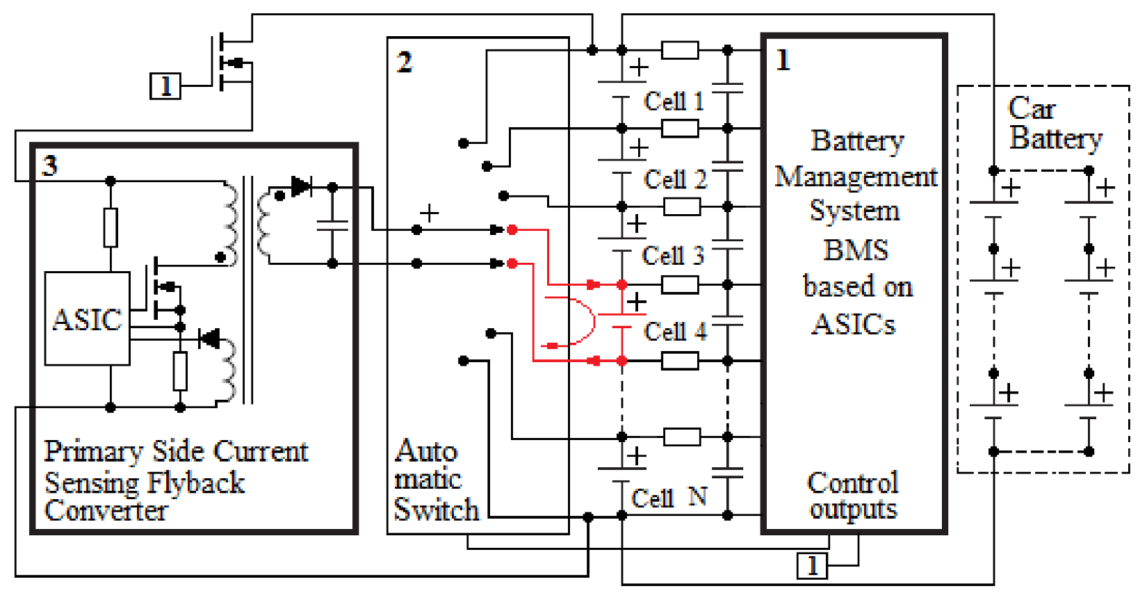
  • The Battery Management System can be based on one of the ASICs LTC6802-2, MAX1894, MAX11068, MAX11080, DS2726, BQ29330, AD7280, and ATA6870 [22,23,24]. This system monitors the overall battery voltage and controls the automatic switch (2) and the flyback converter (3). The BMS is not the object of research in this paper.
  • The automatic switch system. This provides mechanical switching between the cells of the battery, and is also not the object of research in this paper.
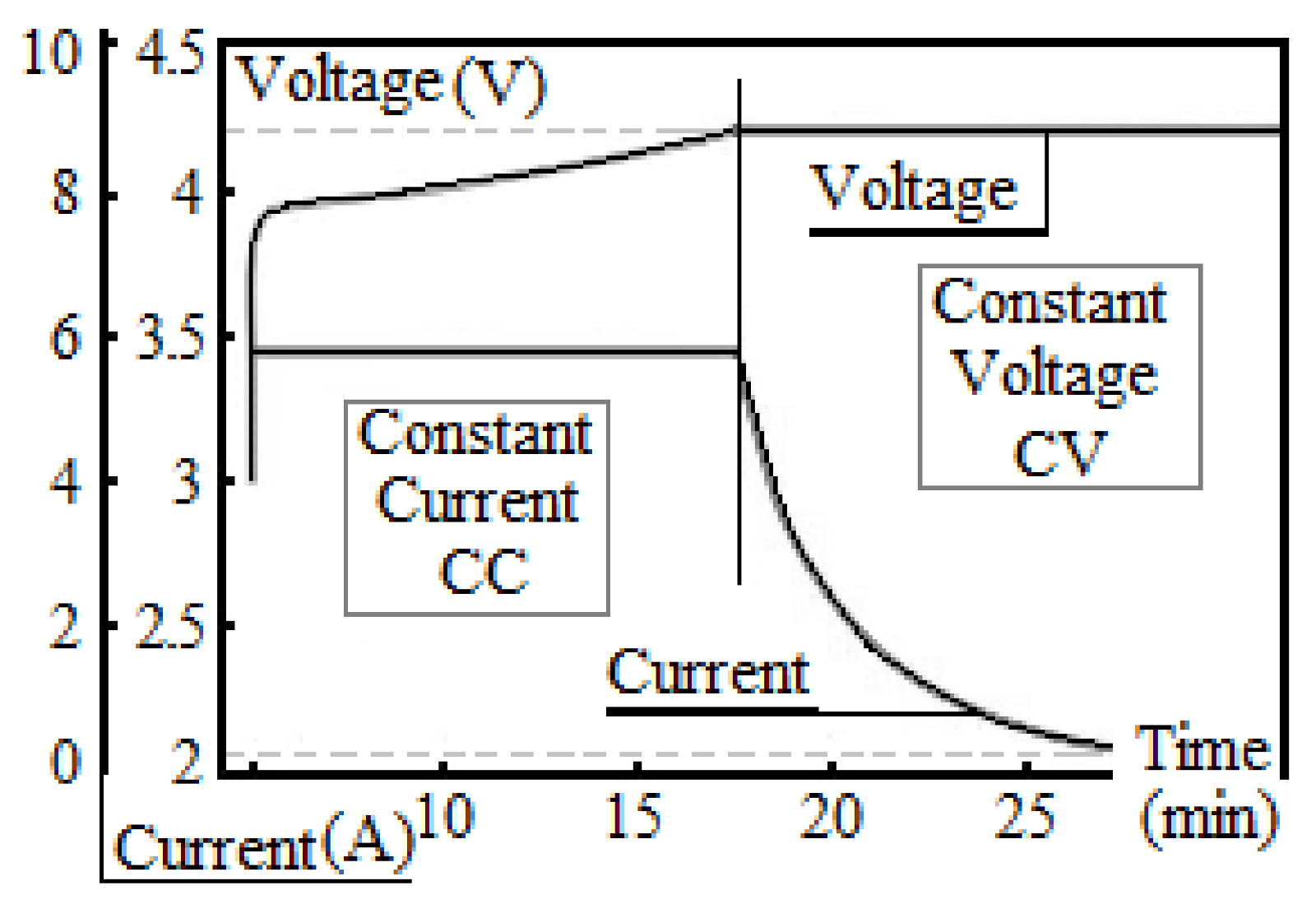
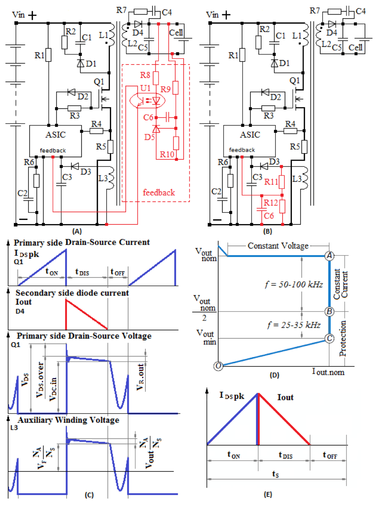
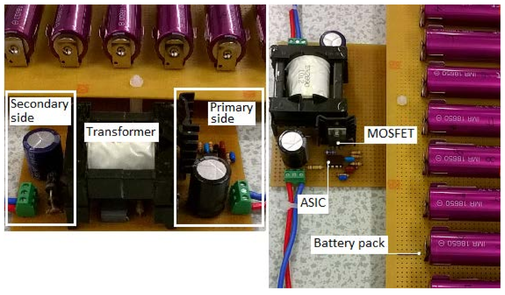
  • Primary side current flyback converter. The schematic is based on ASICs, for example AP3706, FAN104W, FL103, or MP020-5 [16,17,19,20]. This converter is used for the charging of a single cell (within a series string within a battery pack) if its voltage is lower than that of the other cells in the string. The charging process is conducted according to the CC (constant current) and CV (constant voltage) procedure shown in Figure 2.
Figure 3 shows the schematic of the proposed converter (Figure 3B) and its derivation from a classical flyback converter (Figure 3A) with a feedback circuit. In the former, the omitted feedback schematic requires information about the output voltage to be taken from the auxiliary winding (L3) and about the output current from the current sense resistor ( R 5 ).
Figure 3C–E show the discontinuous conduction mode of operation (DCM), the V-I characteristic of the converter, and the time sequence of operation required for the DCM, respectively. The secondary voltage measurement is based on the oscillation process occurring over the transistor Q 1 (Drain-Source) during the current pause, t OFF . It can be seen in Figure 3C that the voltage across Q 1 (the Drain-Source), V DS , is the sum of the input voltage, V in , the output reflecting voltage, V R . out , and the over voltage, V DS . over . The output voltage reference can be obtained through the auxiliary winding ( L 3 ), which is normally used as a power supply for the ASIC (Figure 3A). The voltage from the winding L 3 and the divider R 11 R 12 must meet the ASIC range, which is usually between 2 and 5 V depending on the manufacturer’s requirements. In this way, a reference for the output voltage is given to the control system without the classical feedback circuit shown in Figure 3A.
The operation of the converter follows the next time sequence (Figure 3E):
  • Time t ON : the input voltage V DC . in is applied across the primary side of the transformer ( L 1 , Figure 3B), which increases the primary side current from zero to the peak value ( I DC . pk ).
  • Time t DIS : the primary side transistor ( Q 1 ) is turned off and the rectifier on the secondary side ( D 4 ) is turned on. The secondary side current decreases linearly to zero. At its zero point, the accumulated energy in the transformer is depleted.
  • The time t OFF : the primary side voltage across Q 1 and the voltage across L 3 begins to oscillate on the resonance frequency between the primary side inductance and the parasitic output capacitor.
Figure 3D shows the Constant Voltage (CV) and Constant Current (CC) operational area described earlier in Figure 2. Assuming that the converter works only as an additional charger for SoC equalisation, this suggests that an entire cycle of charging from 0% to 100% will not be done from this charger. It can be proposed that the operation mode coincides with point A where fast charging is possible. This means that the converter must operate with higher efficiency at that point. The other two points, point B 50% of nominal output voltage and point C minimum output voltage, are also an important part of the calculation procedure.

3. Design Procedure

The design procedure depends on the parameters of the specific ASIC [16,17,19,20], which vary depending on the manufacturer. Because of this, the design procedure suggested here shows the common application of a DC-DC flyback converter with primary side sensing. The design procedure is now described in detail.

3.1. Input Parameters

The successful design requires precise input parameters: V in . nom is the nominal input voltage. In this case, this is the voltage from the vehicle battery where the minimum and maximum tolerances must also be given as V in . min and V in . max . V out . nom and I out . nom are the nominal output voltage and current, respectively, considered according to the cell parameters shown in Figure 2. The output power is defined as P out . nom = I out . nom × V out . nom . Other parameters, such as temperature tolerances, size, weight, power density, and price, currently are not under consideration.

3.2. Estimation of the Efficiency

The input nominal power P in . nom is given as:
P in . nom = V out . nom × I out . nom η .
The overall nominal efficiency at the beginning can be assumed to be within a wide range η overall 75 85 % . Although there is no input rectifier and filter due to the relatively low output voltage, a greater efficiency than 85% for this class of converter cannot be expected.
From Equation (1), the input power at point B ( P in . B ) and point C ( P in . C ) can be derived according to the next assumption: at point B, the output voltage drops to 50% of the nominal voltage and the overall efficiency falls to η overall . B = 50 % ; at point C, the efficiency and the input power depend on the minimum output voltage. With these assumptions, Equation (1) can be written for P in . nom . B efficiency at point B, η overall . B , as follows:
P in . nom . B = 0.5 × V out . nom × I out . nom η overall . B
where the efficiency at point B, η overall . B , can be calculated from the overall efficiency, η overall , and the secondary side diode forward-voltage drop, V F , as:
η overall . B η overall × 0.5 × V out . nom ( 0.5 × V out . nom + V F ) × ( V out . nom + V F ) V out . nom .
At point C, the converter works at the minimum output voltage, V out . min , where the input power and the efficiency at this point, η overall . C , are respectively:
P in . C = V out . min × I out . nom η overall . C
η overall . C η overall × V out . min ( V out . min + V F ) × ( V out . nom + V F ) V out . nom .
Point A is the working point for the converter if it works on fast charge mode. The input power at that point will be:
P in . A = V out . out × I out . nom η overall = V out . out × I out . nom 75 85 %
where as a first assumption 80% overall efficiency can be accepted.

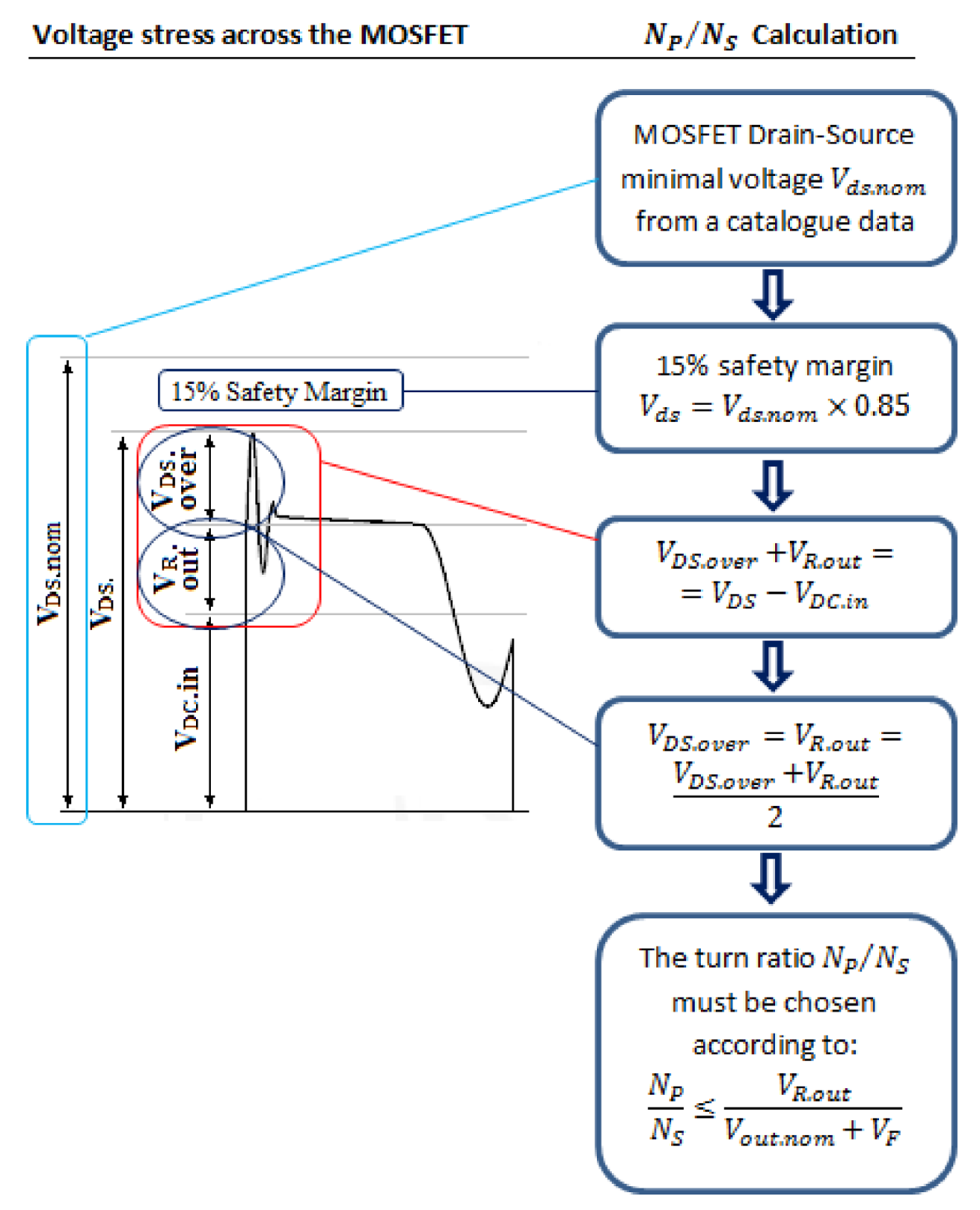
3.3. Determination of the Transformer Turns Ratio

The suggested design procedure begins with transformer turns ratio determination as opposite to the established flyback design procedures [25,26] with optical feedback connections (Figure 3A). The transformer turn ratio parameter represents the ratio between the primary and secondary turns N P / N S . It must be chosen as a compromise between the primary and secondary voltage stress, respectively, over the transistor ( Q 1 , Figure 3B) and the diode ( D 4 , Figure 3B).
As can be seen in Figure 3C, when the transistor is turned off, the voltage drain-source ( V DS ) will be the sum of the input voltage ( V DC . in ) and the reflected output voltage ( V R . out ):
V DS = V DC . in + V R . out + V DS . over
where the reflected output voltage ( V R . out ) can be calculated according to the transformer turn ratio ( N S / N P ) , i.e., secondary, N S , and primary, N P :
V R . out = N S N P × ( V out + V F ) .
V DS . over is the overvoltage caused by the leakage inductance. In this design, N P / N S is estimated according to the desired MOSFET type with respect to its nominal voltage drain-source. The calculation algorithm and the primary side voltage stress over Q 1 are shown in Figure 4 according to the parameters assumed in Figure 3C.
The overvoltage V DS . over and the entire oscillating process depend on several parameters, including random factors, such as primary side and leakage inductance, transistor output capacitance, and PCB (Printed Circuit Board) layout issues, which cannot be precisely determined. This means that the overvoltage must be verified experimentally.
The transformer turns ratio between the auxiliary winding L 3 and the secondary winding L 2 ( N A / N S ) depends on the ASIC voltage supply range. Because fast charging is a heavy load, a relatively high overvoltage V DS . over can be expected, and this must be taken into consideration. With the minimum, V DD . min , and maximum, V DD . max , voltages the auxiliary winding can be calculated from:
V DD . min = N A N S × ( V out . min + V F + N S N P × V DS . over ) V F . aux
V DD . max = N A N S × ( V out . nom + V F + N S N P × V DS . over ) V F . aux
where V F . aux is the forward voltage drop across the diode ( D 4 , Figure 3B).

3.4. Design of the Transformer

According to the time periods shown in Figure 3E, the sum of the primary side (transistor Q 1 ) and the secondary side (rectifier D 4 ) conduction time at point B (Figure 3D), i.e., 50% of the output voltage V out . nom , is given by:
t ON . B + t DIS . B = 1 f S t OFF . B ( 1 + N S N P × V DC . min . B 0.5 × V out . min + V F . aux ) × ( 1 + N S N P × V DC . min . B 0.5 × V out . min + V F . aux )
where V DC . min . B is the minimum input voltage at point B.
From here, the sum of t ON . B + t DIS . B is derived as:
t ON . B + t DIS . B = 1 f S t OFF . B
where f s is the switching frequency. The primary transformer inductance, L m , is given by:
L m = ( V in . B × t ON . B ) 2 × f S 2 × P in . nom . B .
The maximum primary side peak current, I DS . pk , (Drain-Source) is given by:
I DS . pk = 2 × P in . nom L m × f s .
The minimum number of turns required to avoid core saturation is given by:
N p . min = L m × I DS . pk B sat × A e
where B sat is the flux density (T), and A e is the cross-sectional area ( m 2 ) .
At point C, the converter operates in discontinuous conducting mode and the ON ( t ON . C ) and OFF ( t OFF . C ) times at this point must be checked according to:
t ON . C = 1 V bus . min . C × 2 × P in . C × L m f s . r
t OFF . C = 1 f s . r t ON . C ( 1 + N P N S × V in . min . C V out . min + V F )
where f s . r is the switching frequency after its reduction (Figure 3B).
The transformer turns ratio between the auxiliary winding N A and the secondary winding N S depends on the supply voltage ( V DD ) of the ASIC used. As the voltage on the auxiliary winding varies with the output load, it is important to operate within the permissible voltage range. In the case that the voltage V DD drops down below the minimum threshold, V DD . min , the converter must stop working. The following condition must be satisfied:
V DD . min = ( N A N S ( V o + V F ) V F . aux ) > V DD . max + ( 2 3 V )
where V DD . max is the maximum allowable voltage and ( 2 3 V ) is a safety merging.
The transformer core, usually ferrite for flyback converters [18,19], must be selected according to the output power. Its selection can be made from the product parameter A E A W :
A E A W = ( L m × I DS . pk × I DS . rms × 10 4 B max × K u × K j × f S . min )
where A E is the core cross-sectional area, A W the window area available for winding, K u the winding factor (0.25–0.3), K j the current density coefficient (400–600), B max the maximum flux density or saturation flux density of the core material, and f S . min the minimum frequency.
With a given core size, the primary winding turns, N p , is given by:
N p = L m × I DS . pk A E × B max .
The wire size can be chosen according to the RMS (Root Mean Square) primary current 2.5 3   A / mm 2 . Multiple strands with diameters d depend on the frequency:
d = 1 π . f s . μ 0 . σ
where: μ 0 = 4   × π × 10 7   H / m is the permeability in vacuum and σ = 6 × 10 7   S / m is the conductivity of the copper. The magnetic air gap length in the core is:
l gap = μ o . A E . N p 2 L m l c μ r μ o . A E . N p 2 L m
where μ r is the relative magnetic permeability of the core material and l c the core magnetic length.
The stored energy, E st , in the flyback transformer is given from:
E st = 1 2 . L m . I DC . pk 2 . f s .

3.5. Current Sense Resistor

The current sense resistor ( R 5 ) value is calculated by:
R 5 = N p K × I out × N s
where K is the design parameter of the ASIC. The voltage divider R 11 R 12 can be calculated from:
R 11 R 12 = V out . nom V ref × N A N s 1 .
The capacitor C6 must be chosen in the range 22 ÷ 68   pF [19].

3.6. Calculating the Parameters of the Primary Side MOSFET Transistor

The voltage stress of the primary side transistor is given in Figure 4. The Drain-Source primary RMS current, I DS . rms , is calculated from:
I DS . rms = I DS . pk × t ON × f s 3 .

3.7. Calculating the Parameters of the Secondary Side Rectifier

The maximum reverse voltage and the RMS current of the secondary side rectifier are given from:
V F = V out . nom × N S N P × V in . max
I F . rms = I DS . rms × V DC . in . min V R . out × N P N S .
Equation (28) is based on I DS . rms and the transformer turn ratio.
The relationship between the primary and the secondary side peak current is:
I DS . pk = I F . pk N p
where I F . pk is the secondary side peak current. The dependence between the ideal output current, I out , and I F . pk is given by:
I out = 1 2 × I F . pk × t ON t s .

3.8. Design of the Clamping Systems

The parasitic components, such as leakage inductance L LK , secondary leakage inductance L LKS , output MOSFETs capacitance C oss , and secondary rectifier capacitance C DS , are analysed [26,27,28] and included in this design procedure.
The primary side RCD clamping circuit ( R 2 , C 1 , D 1 ) prevents the excessive voltage spike which results from the transformer leakage inductance ( L LK ). The maximum voltage stress of the MOSFET is given by Equation (7). The previously considered safety voltage margin of 15% shows that the clamping system must restrict the voltage spike in this range. The peak clamping current is given from:
I CL . pk = ( 2 . P IN . A L m . f s ) 2 C oss L LK V DC . over 2
where C oss is the output capacitance of the transistor Q 1 taken from the manufacturer’s catalog.
The dissipated power from the RCD network, P RCD , is given by:
P RCD = 1 2 f S . L LK . I CL . pk 2 . V R . out + V DC . over V DC . over .
The resistance R 2 and the capacitor C 1 are given by:
R 2 = ( V R . out + V DS . over ) 2 P RCD
C 1 > V R . out + V DS . over   V rip . R RCD . f s .

3.9. Design of the Output Filter

The peak-to-peak ripple, I C . rip , of the output capacitor ( C 5 ) is calculated from:
I C . rip =   N p N s I DS . pk ,
and the voltage ripple on the output from:
V out . rip = t DIS . A 2 . C 5 × ( I C . rip I out . nom ) 2 I C . rip + I C . rip × R ESR
where R ESR is the equivalent series resistor of C 5 .

3.10. Design of the RC Snubber

The resistor R 7 is given by:
R 7 = L LKS C DS
where L LKS is the secondary leakage inductance and C DS is the secondary side rectifier parasitic capacitance.
Normally C 4 is 2–3 times C DS .

4. Experimental Results

Based on the presented design procedure, an experimental converter was designed, built, and tested. Its parameters are presented in Table 1.
The experimental results are presented as follows:
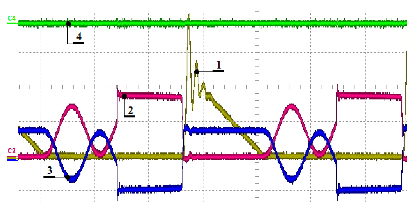
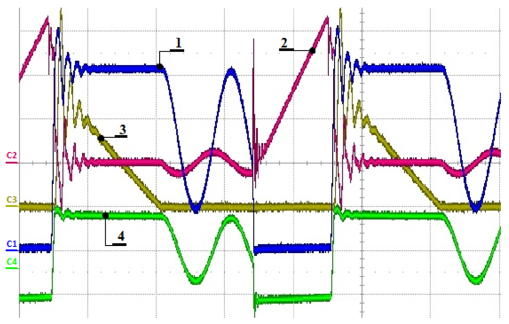
  • Figure 5. The oscillogram shows the primary side of the converter, where: (1) is the voltage Drain-Source, V DS , across the MOSFET with specific oscillation after full energy transfer; (2) is the primary side current, I pk , through L 1 , Q 1 , and R 5 ; (3) is the secondary side current through the rectifier, which represents the energy transfer at the zero point; and (4) is the voltage on the auxiliary winding, which repeats the shape of (1) but with a smaller amplitude.
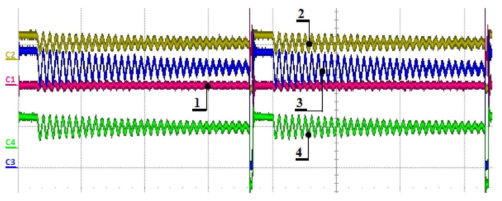
  • Figure 6 shows the secondary side of the converter, where (1) and (2) are the secondary side current and voltage, respectively, over D 4 ; (3) is the voltage on the auxiliary winding; and (4) is the output voltage.
  • Figure 7 shows the primary side of the converter under an open circuit. Although the tested battery charger is not supposed to work under this condition, this experiment shows the process of reducing the switching frequency from 50–100 kHz to 20–35 kHz (Figure 3D).
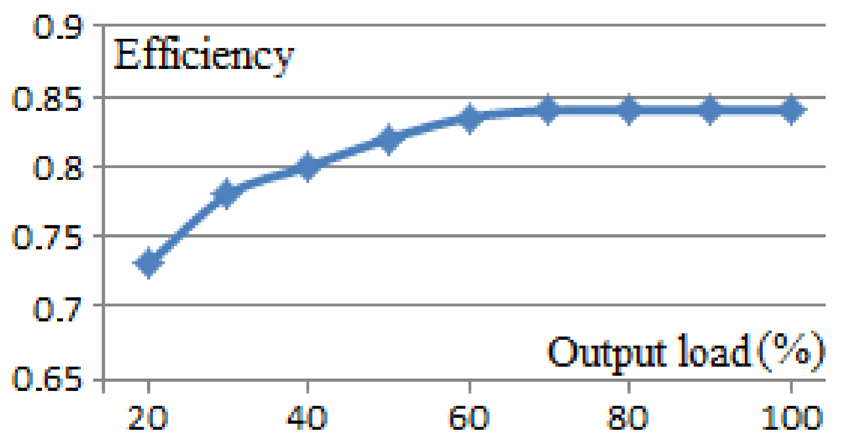
  • The maximum obtained efficiency of the converter is 84% as shown in Figure 8.
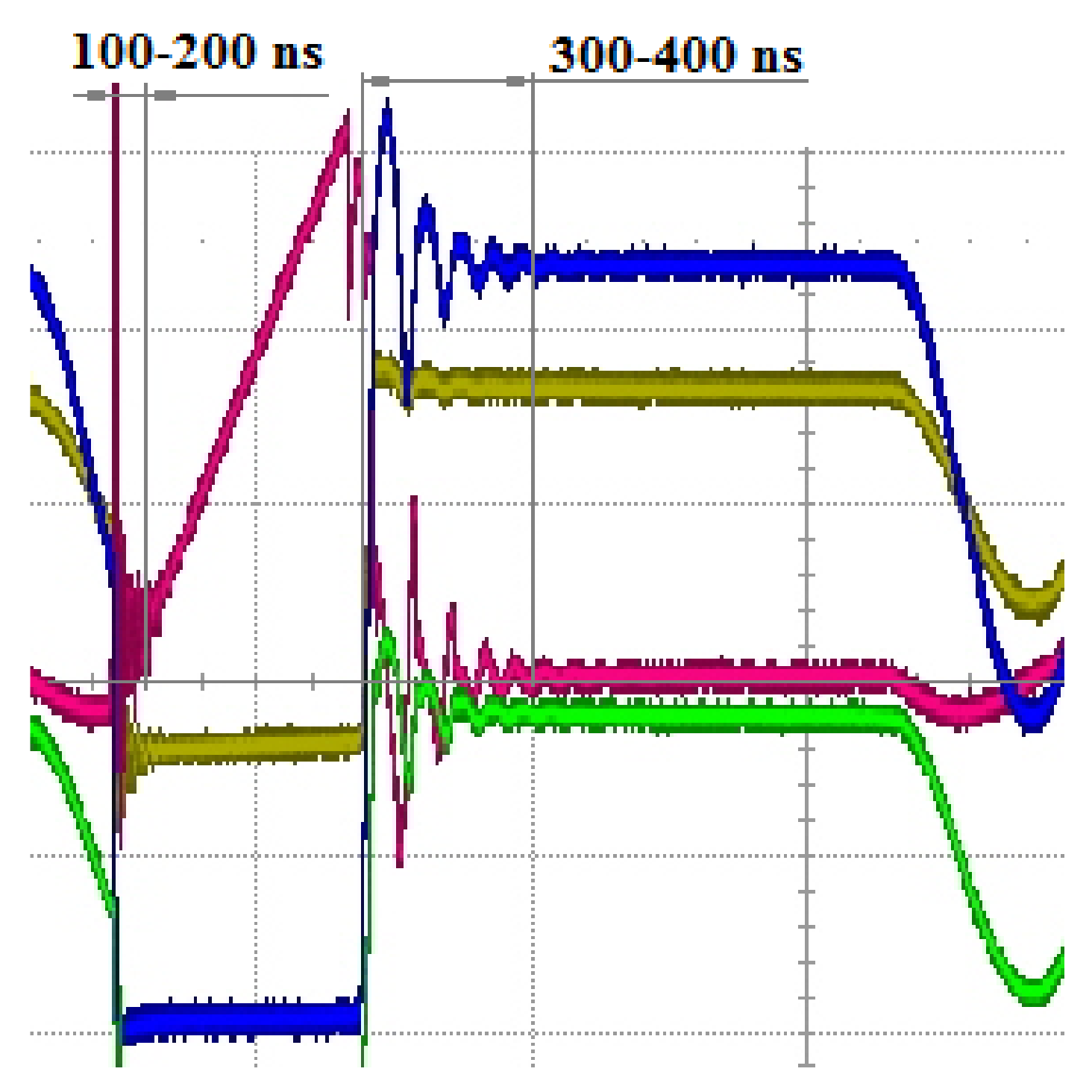
  • Some specific parameters are given in Figure 9. The primary side current has a peak value immediately after the transistor is turned on. When it is turned off, its process has a typical oscillation in V DS . Although these features are assumed to be normal, they have to be considered alongside the control system parameters. Two delay times are necessary for its correct operation, respectively, in ranges 100–200 ns and 300–400 ns as Figure 10 shows.
A photo of the experimental converter and a battery string is shown in Figure 10.

5. Conclusions

In this paper, the essential points of the design procedure of a flyback converter with primary current sensing is presented. The same converter can be used as part of a BMS for active cell balancing. From the obtained results, the following conclusions can be formulated:
  • The presented design procedure for a DC-DC flyback converter is correct and it can be used as part of the overall design of the converter.
  • The schematic of the flyback converter with primary current sensing (Figure 3B) can be used as a battery charger and is particularly suitable for battery equalisation as part of a BMS. The schematic works under constant current and constant voltage (Figure 3D) and meets the battery charging requirements (Figure 2).
  • The efficiency of the circuit reaches 82–84% for a low-voltage output converter (Figure 8). If fast charging of a cell is necessary, the converter must be designed to work at the working point A from the output V-I characteristic (Figure 3 D).
  • The experimental verification shown in Figure 5, Figure 6 and Figure 7 entirely meets the theoretical analysis shown in Figure 3.
  • As Figure 9 shows, the two delay times in the turn-on and turn-off processes are necessary.

Acknowledgments

This work is supported by an EPSRC research grant “ELEVATE—ELEctrochemical Vehicle Advanced TEchnology”, EP/M009394/1.

Author Contributions

Borislav Dimitrov and Andrew Cruden conceived and designed the experiments; Borislav Dimitrov and Muthu Krishna performed the experiments; Borislav Dimitrov, Andrew Cruden and Suleiman Sharkh analysed the data; Borislav Dimitrov, Andrew Cruden, Muthu Krishna and Ahmad Elkhateb contributed to the circuit design, design procedure and analysis; Borislav Dimitrov and Andrew Cruden wrote the paper.

Conflicts of Interest

The authors declare no conflict of interest.

References

  1. Jang, J.; Zhang, C. Fundamentals and Applications of Lithium-ion Batteries in Electric Drive Vehicles; John Wiley & Sons: Singapore, 2015; ISBN 978-1-118-41478-1. [Google Scholar]
  2. Link, A.; O’Connor, A.; Scott, T. Battery Technology for Electric Vehicles; Swales & Willis Ltd.: Devon, UK, 2015; ISBN 978-1-138-81110-2. [Google Scholar]
  3. Brec, E.; Muller, B. Electric Vehicle Batteries: Moving from Research Towards Innovation; Springer International Publishing: Cham, Switzerland, 2015; ISBN 978-3-319-12705-7. [Google Scholar]
  4. Andrea, D. Battery Management System for Large Lithium-Ion Battery Packs; Artech House: Boston, MA, USA; London, UK, 2010; ISBN 978-1-60807-104-3. [Google Scholar]
  5. Namith, T.; Shankpal, P. Design and Development of Efficient Battery Charging and Cell Balancing for Battery Management System. SASTech J. 2012, 11, 15–22. [Google Scholar]
  6. Douglass, J. Battery Management for High-Power Battery Stacks. CAN Newsletter 4/2010. 2010, pp. 34–38. Available online: https://can-newsletter.org (accessed on 15 August 2017).
  7. Hoog, J.; Alpcan, T.; Brazil, M.; Thomas, D.; Mareels, I. Optimal Charging of Electric Vehicles Taking Distribution Network Constraints into Account. IEEE Trans. Power Syst. 2014, 30, 365–375. [Google Scholar] [CrossRef]
  8. Li, L.; Lu, X.; He, J.; Sun, Z.; Yang, G. Design of New-generation Electric Vehicle Terminal. Energy Power Eng. 2013, 5, 1362–1366. [Google Scholar] [CrossRef]
  9. Barreras, J.; Swierczynski, M.; Schaltz, E.; Andreasen, J.; Christian, F.; Sauer, D.; Dirk, U. Christensen Functional Analysis of Battery Management Systems Using Multi-Cell HIL Simulator. In Proceedings of the 10th International Conference on Ecological Vehicles and Renewable Energies (EVER), Monte-Carlo, Monaco, 31 March–2 April 2015. [Google Scholar]
  10. Gi-Heon, K.; Jeffrey, G.; Lustbader, J.; Pesaran, A. Thermal Management of Batteries in Advanced Vehicles Using Phase-Change Materials. World Electr. Veh. J. 2008, 2, 137–147. [Google Scholar]
  11. Paul, C.; Chao, P.; Chen, W.; Wu, R. A Battery Charge Controller Realized by a Flyback Converter with Digital Primary Side Regulation for Mobile Phones. Microsyst. Technol. 2014, 20, 1689–1703. [Google Scholar]
  12. Mayuri, R.; Purushotham, K.; Rao, B. High Efficient AC/DC Converter. Elect. Electron. Eng. 2017, 7, 43–47. [Google Scholar]
  13. Qiu, J.; He, L.; Wang, Y. A Multimode Digital Controller IC for Flyback Converter with High Accuracy Primary-Side Feedback. Comput. Electron. 2013, 14, 652–662. [Google Scholar] [CrossRef]
  14. Lian, K.; Hong, C. Current-Sensorless Flyback Converters Using Integral T-S Fuzzy Approach. Int. J. Fuzzy Syst. 2013, 15, 66–74. [Google Scholar]
  15. Chang, C.; Lin, Y.; Tzou, Y. Digital Primary-Side Sensing Control for Flyback Converters. In Proceedings of the International Conference on Power Electronics and Drive Systems, Taipei, Taiwan, 2–5 November 2009; pp. 689–694. [Google Scholar]
  16. Monolithic Power Systems (MPS). Application Note AN062 Rev.12, Flyback Converter Using the Primary-Side Regulator, 2012, MP020-5. Available online: https://www.monolithicpower.com/ (accessed on 15 August 2017).
  17. Qinghua, S.; Wengui, D. Basic Steps to Design a PSR Flyback Converter Using AP3706/08N, 2009, BCD Semiconductor Manufacturing Limited Application Note 1028, Rev 1.1. Available online: https://www.diodes.com/ (accessed on 15 August 2017).
  18. Fairchild Semiconductor Corporation Design Guideline for Flyback Charger Using FAN104WMX, 2012, Application Note AN-6093 Rev. 1.0.1. Available online: https://www.fairchildsemi.com (accessed on 15 August 2017).
  19. Fairchild Semiconductor Corporation, Design Guideline for LED Lamp Control Using Primary-Side Regulated Flyback Converter, FL103M, 2011, Application Note AN-9741 Rev. 1.0.0. Available online: https://www.fairchildsemi.com (accessed on 15 August 2017).
  20. ST Datasheet Production Data. Off-Line All-Primary-Sensing Switching Regulator. 2014. Available online: https://www.st.com (accessed on 15 August 2017).
  21. Ayachit, A.; Reatti, A.; Kazimierczuk, M.K. Magnetising Inductance of Multiple-Output Flyback DC-DC Convertor for Discontinuous-Conduction Mode. IET Power Electron. 2016, 10, 451–461. [Google Scholar] [CrossRef]
  22. Analog Devices Inc. Lithium Ion Battery Monitoring System AD7280. 2008. Available online: https://www.analog.com (accessed on 15 August 2017).
  23. Maxim Integrated Products, Inc. 5-Cell to 10-Cell Li+ Protector with Cell Balancing. 2010. Available online: https://www.maxim-ic.com (accessed on 15 August 2017).
  24. Maxim Integrated Products, Inc. 12-Channel, High-Voltage Battery-Pack Fault Monitors. 2010. Available online: https://www.maxim-ic.com (accessed on 15 August 2017).
  25. Saliva, A. Design Guide for Off-Line Fixed Frequency DCM Flyback Converter, Infineon Technologies North America, Design Note DN 2013-01. Available online: https://www.infineon.com (accessed on 15 August 2017).
  26. Saini, D.; Ayachit, A.; Reatti, A.; Kazimierczuk, M.K. Analysis and Design of Choke Inductors for Switched-Mode Power Inverters. IEEE Trans. Ind. Electron. 2018, 65, 2234–2244. [Google Scholar] [CrossRef]
  27. Luchetta, A.; Manetti, S.; Piccirilli, M.; Reatti, A.; Kazimierczuk, M. Effects of Parasitic Components on Diode Duty Cycle and Small-Signal Model of PWM DC-DC Buck Converter in DCM. In Proceedings of the IEEE 15th International Conference on Environment and Electrical Engineering, Rome, Italy, 10–13 June 2015; pp. 772–777. [Google Scholar]
  28. Luchetta, A.; Manetti, S.; Piccirilli, M.; Reatti, A.; Kazimierczuk, M. Derivation of Network Functions for PWM DC-DC Buck Converter in DCM Including Effects of Parasitic Components on Diode Duty-Cycle. In Proceedings of the IEEE 15th International Conference on Environment and Electrical Engineering, Rome, Italy, 10–13 June 2015; pp. 778–783. [Google Scholar]
Figure 1. The basic schematic of the battery management system (BMS) and the DC-DC converter for battery voltage equalisation. (1) BMS based on an Application Specialised Integrated Circuit (ASIC); (2) automatic switch; (3) primary side current-sensing flyback converter based on the ASIC.
Electronics 07 00043 g001
Figure 2. Li-ion battery charge diagram. CC: Constant Current charge; CV: constant voltage charge.
Electronics 07 00043 g002
Figure 3. (A,B) Development of the flyback converter with primary current sensing from the classical flyback converter with optocoupler-based feedback; (C) Current-time and voltage-time diagrams of the primary and secondary side currents, primary side voltage over MOSFET Q1, and primary side voltage on the auxiliary winding L 3 ; (D) Output V-I diagram of the converter during CC (constant current), CV (constant voltage) operation mode; (E) Lengths of the operating cycle.
Electronics 07 00043 g003
Figure 4. Algorithm for calculating the turn ratio N P / N S .
Electronics 07 00043 g004
Figure 5. Primary side of the converter: (1) Voltage Drain-Source V DS over the transistor ( 150.00   V / div ) ; (2) Primary side current I pk ( 0.5   A / div ) ; (3) Secondary side current through the rectifier ( 1.00   A / div ) ; and (4) Voltage on the auxiliary winding ( 5.00   V / div ) . Time scale: 2.5   μ s / div , 100 kHz.
Electronics 07 00043 g005
Figure 6. Secondary side of the converter: (1) Secondary side current through the rectifier ( 2.00   A / div ) ; (2) Voltage over the secondary side rectifier ( 5.00   V / div ); (3) Voltage on the secondary side of the transformer L 2 5.00   V / div ; and (4) Output DC voltage ( 20.00   mV / div ) . Time scale: 2.50   μ s / div ,   100   kHz .
Electronics 07 00043 g006
Figure 7. Primary side of the converter under an open circuit: (1) Primary side current I pk ( 0.5   A / div ) ; (2) Voltage on the auxiliary winding ( 10.00   V / div ) ; (3) Voltage Drain-Source V DS over the transistor ( 200.00   V / div ) ; and (4) Voltage after the auxiliary winding divider R 11 ,   R 12 , and C 6 (Figure 3B) ( 2.00   V / div ) ; Time scale: 10   μ s / div ,   25   kHz .
Electronics 07 00043 g007
Figure 8. Efficiency of the experimentally tested converter.
Electronics 07 00043 g008
Figure 9. The delay times during the transient processes when turning on and off.
Electronics 07 00043 g009
Figure 10. The Experimental converter with a battery string.
Electronics 07 00043 g010
Table 1. Parameters of the experimentally tested converter.
ParameterValue
V in . min 350 V
V in . max 400 V
V in . nom 380 V
V out . max 5 V
I out . max 10 A
f s 66 kHz

