X-Band GaN Power Amplifier MMIC with a Third Harmonic-Tuned Circuit
by
Kyung-Tae Bae
1, 
Ik-Joon Lee
1,
Byungjoo Kang
2,
Sanghoon Sim
2,
Laurence Jeon
2 and
Dong-Wook Kim
1,* 1
Department of Radio Science and Engineering, Chungnam National University, Daejeon 34134, Korea
2
RFcore Co., Ltd., #C-708, Pundang Techno-Park, 744 Pangyo-ro, Yatap-dong, Pundang-gu, Sungnam, Gyeonggi 13510, Korea
*
Author to whom correspondence should be addressed.
Electronics 2017, 6(4), 103; https://doi.org/10.3390/electronics6040103
Submission received: 21 November 2017
/
Revised: 24 November 2017
/
Accepted: 24 November 2017
/
Published: 28 November 2017
Abstract
:This paper presents an X-band GaN HEMT power amplifier with a third harmonic-tuned circuit for a higher power density per area and a higher power-added efficiency (PAE) using a 0.25 μm GaN HEMT process of WIN semiconductors, Inc. The optimum load impedances at the fundamental and third harmonic frequencies are extracted from load-pull simulations at the transistor’s extrinsic plane, including the drain-source capacitance and the series drain inductance. The third harmonic-tuned circuit is effectively integrated with the output matching circuit at the fundamental frequency, without complicating the whole output matching circuit. The input matching circuit uses a lossy matching scheme, which allows a good return loss and a simple LC low-pass circuit configuration. The fabricated power amplifier monolithic microwave integrated circuit (MMIC) occupies an area of 13.26 mm2, and shows a linear gain of 20 dB or more, a saturated output power of 43.2~44.7 dBm, and a PAE of 35~37% at 8.5 to 10.5 GHz.
1. Introduction
RF front-ends of X-band airborne phased array radars and satellite synthetic aperture radar (SAR) systems are composed of transmit/receive (T/R) modules with various monolithic microwave integrated circuit (MMIC) chips [1,2]. Since the array size in a radar is susceptive to the size or volume of the T/R module, there have been efforts to reduce it, especially for airborne applications requiring limited payloads [3]. Recently, thanks to GaN technology, which provides better power capabilities than Si or GaAs technology, the size of the power amplifier MMIC has been dramatically reduced, leading to a smaller-sized T/R module [4,5]. Regarding the cost, currently available commercial GaN HEMT foundry processes are still expensive, compared with Si or GaAs processes, and circuit designers are hence continuing to maximize the number of MMIC chips on a wafer through an area-efficient circuit design for low production cost of the MMICs and T/R modules.
As another design issue, the power-added efficiency of a power amplifier is one of the most challenging concerns. Generally, a power amplifier in a transmitter consumes the most power in the RF front-end and suffers from a thermal dissipation problem affecting the system reliability. The phased array radar has densely-placed thermal sources and cannot efficiently dissipate the generated heat due to a limited space, and requires a high power-added efficiency for the power amplifier. A high-efficiency power amplifier is usually realized using a switching mode such as class E, class F or class J, whose second harmonic impedance is purely reactive. However, the class-E power amplifier is sensitive to inherent parasitic capacitances of the transistor in a GHz frequency range. In addition, it is difficult to define optimum load impedances at harmonic frequencies clearly at the intrinsic current generator plane in the class-F and class-J power amplifiers, without an accurate large-signal equivalent circuit model of the transistor [6,7,8]. Since a typical high-power amplifier MMIC with a power capability of tens of watts has a corporate configuration combining a large number of transistors in parallel, the design of a switching-mode power amplifier, which should meet matching conditions at several harmonic frequencies, tends to increase circuit complexity, thereby increasing the circuit size. To address this issue in an X-band high-power amplifier MMIC, several groups have attempted to improve the power-added efficiency by optimizing one or two harmonics without adhering to specific amplifier classes [9,10,11,12].
In this paper, we present an X-band GaN high-power amplifier MMIC whose efficiency and bandwidth performance are improved by third harmonic impedance tuning and lossy matching. The design specifications of the power amplifier MMIC are a linear gain of 20 dB or more, a saturated output power of 43 dBm or more, and a PAE of 35% at 9 to 10 GHz. The MMIC is fabricated using the 0.25 μm GaN HEMT foundry process of WIN semiconductors [13].
2. Device Technology
In this work, we used a 0.25 μm AlGaN/GaN HEMT on SiC process (NP2500MS) from WIN semiconductors, Inc. (Taoyuan City, Taiwan). The GaN HEMT has a source-coupled field plate to minimize charge trapping and dispersion effects, and has backside via-holes inside its source pads to improve thermal dissipation. The transistor has a breakdown voltage of 100 V or more, a typical power density of 4.0 W/mm, and a PAE of 50% at 10 GHz at a continuous-wave (CW) condition. At a drain-source voltage of 28 V, the current gain cutoff frequency and the maximum oscillation frequency of a 2 × 150 μm HEMT are 24.5 GHz and 75 GHz, respectively [13].
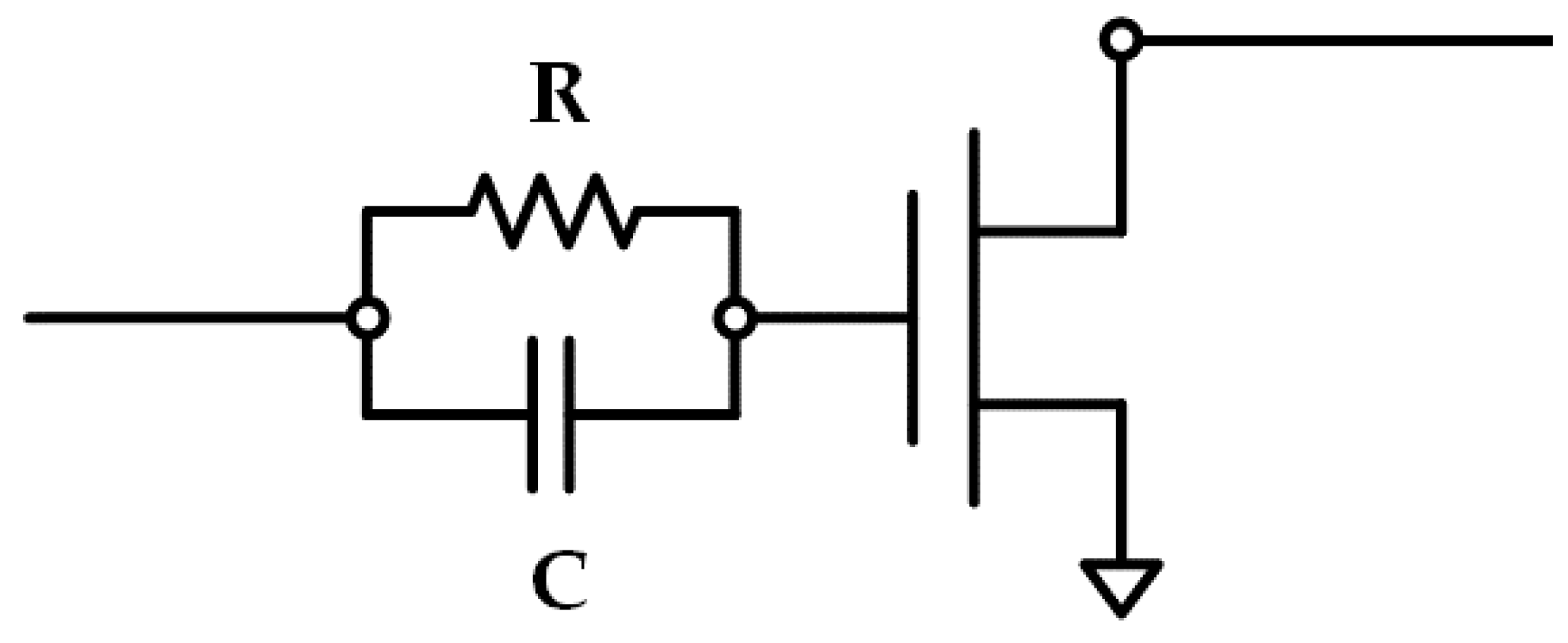
We simulated the small-signal and large-signal performance of 6 × 150 μm and 10 × 150 μm GaN HEMTs using a nonlinear transistor model of WIN semiconductors. The maximum stable gain was 19.3 dB for both transistors at 9.5 GHz under bias conditions of Vds = 28 V and Ids = 100 mA/mm. As shown in Figure 1, a parallel RC circuit is inserted at the gate to ensure unconditional stability of the transistor. The load-pull simulation shows output power and PAE contours of the stabilized 6 × 150 μm and 10 × 150 μm GaN HEMTs at 9.5 GHz, as presented in Figure 2a,b. The 6 × 150 μm HEMT has an output power of 35.7 dBm at a load impedance condition for the maximum PAE of 51.5%, and the 10 × 150 μm HEMT has an output power of 37.3 dBm at a load impedance condition for the maximum PAE of 51%.
3. Circuit Design
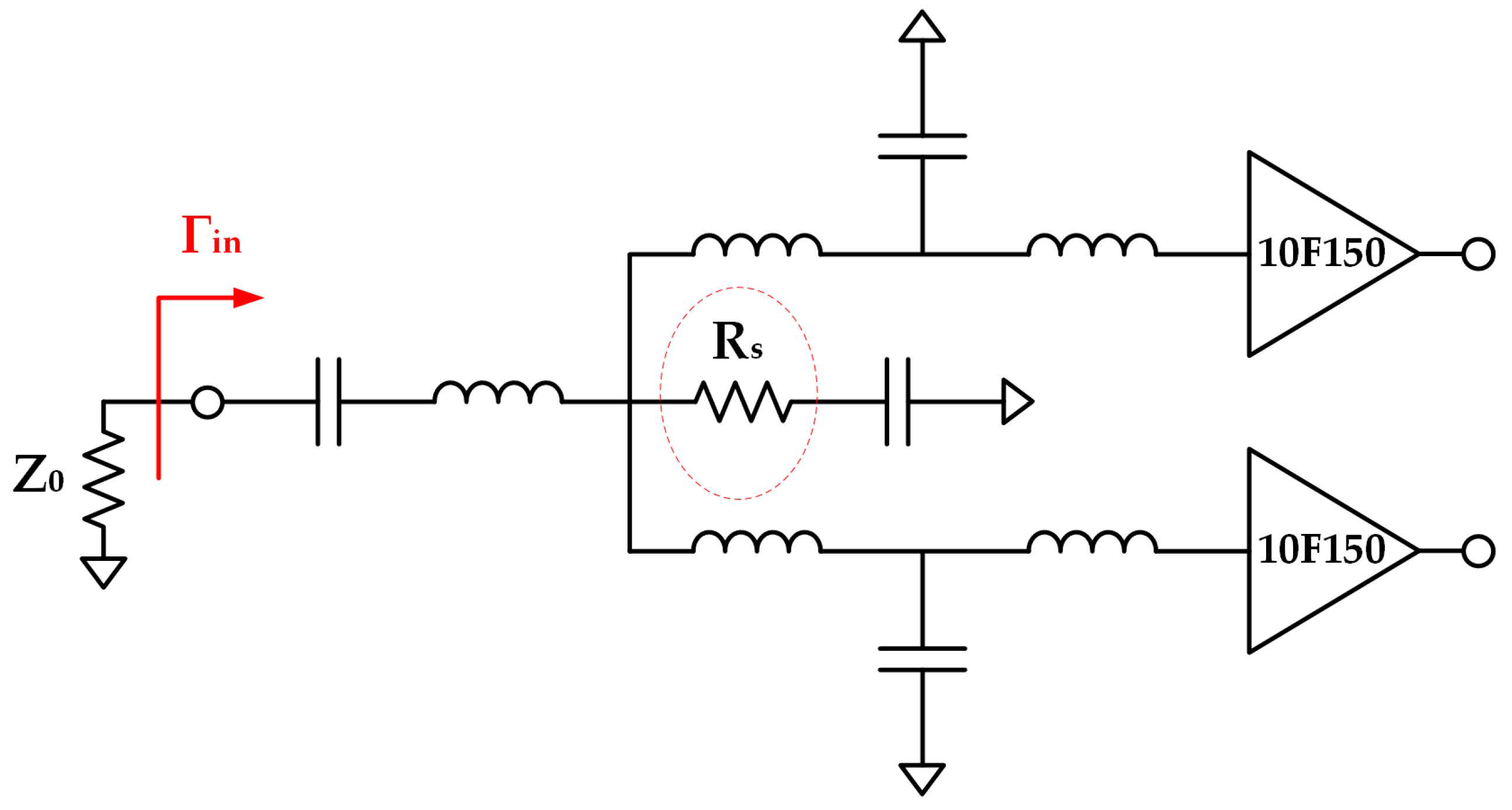
A simple schematic circuit diagram of our X-band high-power amplifier MMIC is illustrated in Figure 3. The power amplifier MMIC uses a two-stage configuration to achieve a linear gain of 20 dB or more. In order to enable the first-stage amplifier to drive the second-stage amplifier sufficiently, we use two 10 × 150 μm (10F150) HEMTs in the first stage and eight 6 × 150 μm (6F150) HEMTs in the second stage, which results in a periphery ratio of 1:2.4. The output matching network is configured by combining a 2:1 impedance transforming circuit and a third harmonic-tuned circuit, and the inter-stage and the input matching circuits utilize a low-pass filtering circuit structure, which is composed of microstrip lines and shunt capacitors. In the following subsections, we describe in detail design schemes including harmonic tuning for efficiency improvement and lossy matching for return-loss improvement.
3.1. Output Matching Circuit Design with the Third Harmonic-Tuned Circuit
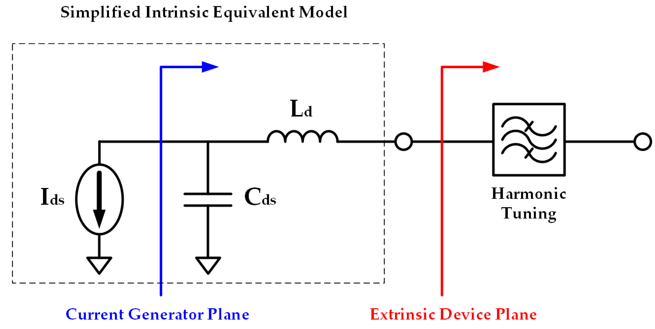
Figure 4 shows a simplified output equivalent circuit model of the transistor where the current generator plane is illustrated with an extrinsic device plane, which is usually encountered in a die transistor or packaged transistor. In a power amplifier such as class F and class J amplifiers, optimum load impedances at multiple harmonic frequencies should be defined at the intrinsic current generator plane. However, since an intrinsic drain-source capacitance Cds and a parasitic inductance Ld cannot be de-embedded from the large-signal nonlinear model provided by the foundry company, it is not practically easy to define the optimum harmonic impedances accurately at the current generator plane. In this work, load-pull simulations are performed at the device’s extrinsic plane to extract the optimum harmonic load impedances, and the simulation results of the 6 × 150 μm HEMT are shown at the fundamental frequency of 9.5 GHz in Figure 5. The simulation conditions are Vds = 28 V and Ids = 100 mA/mm. Figure 5a shows the second-harmonic load-pull simulation results at the condition where the transistor is optimally matched at the fundamental frequency and is open (very high impedance) at the third harmonic frequency, and Figure 5b shows the third-harmonic load-pull simulation results at the condition where the transistor is optimally matched at the fundamental frequency and is open at the second harmonic frequency.
As shown in Figure 5a, the maximum output power and PAE are 35.6 dBm and 52.8% in the second-harmonic load-pull contour plot whose impedance range is −j 20 to −j 1 Ω and almost purely reactive. In Figure 5b, the maximum output power and PAE are 36 dBm and 56.4%, and the third-harmonic optimum load impedance point for them is 0.26 + j 5.9 Ω. Given that the maximum PAE of the 6 × 150 μm HEMT with no harmonic tuning is 51.5%, the PAE increases by 1.3% with the second-harmonic tuning and by 5% with the third harmonic tuning. From the contour plots in the figure, it is noticeable that the PAE degrades very slowly with the second-harmonic impedance condition and varies very rapidly with the third-harmonic impedance condition. As a result, the third-harmonic impedance tuning is very important for the efficiency improvement, and PAE improvement of about 6% can be obtained if the second-harmonic and the third-harmonic load impedances are simultaneously tuned. Both second and third harmonic tuning is not effective in terms of the size of the matching circuit, which requires many elements and occupies a large area. In this work, we focus on only the third-harmonic output impedance tuning, which accounts for most of the PAE improvement.
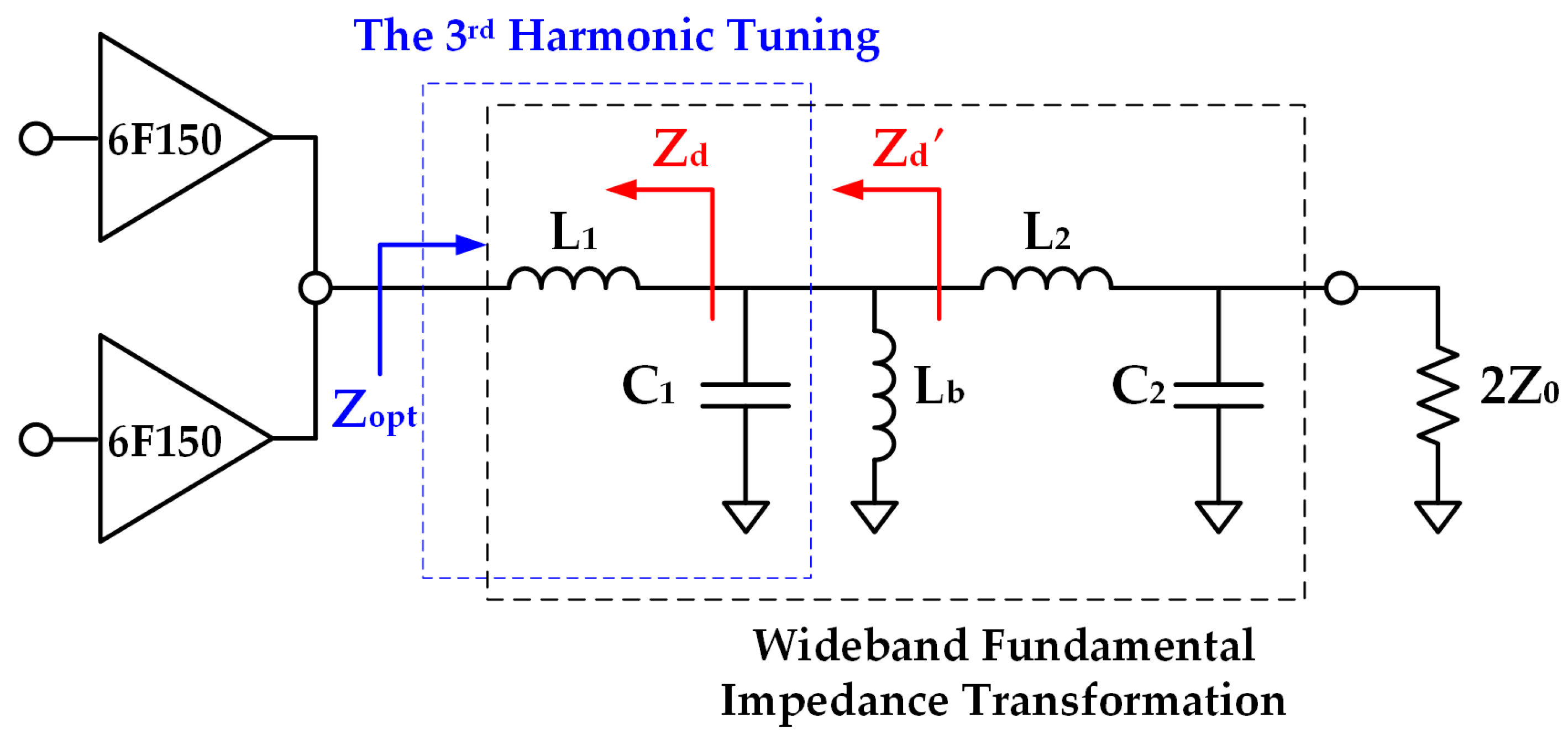
Figure 6 shows an output matching circuit that simultaneously performs the optimum impedance matching at the fundamental frequency and the third-harmonic impedance tuning for two 6 × 150 μm HEMTs. The third-harmonic impedance tuning can be accomplished by placing the third-harmonic load impedance at very low impedance with a shunt capacitor C1 and then moving to the optimum third-harmonic load impedance through a series inductor L1. A parallel inductor Lb is combined with a shunt capacitor C1 to make a parallel LC resonant circuit, where Lb can be used as an RF-choke inductor for a drain bias supply. The parallel LC resonant circuit compensates the reactance of the output impedance Zd including L1 to obtain the impedance Zd’ with a low-Q value, thereby facilitating wideband impedance transformation at the fundamental frequency [14].
The output impedance Zd’ at the fundamental frequency whose reactance is minimized by the parallel LC resonant circuit is matched to 100 Ω through an LC low-pass matching circuit of L2 and C2. Since the matching circuit gives an output impedance of 100 Ω, output impedance of 50 Ω is obtained when the circuits in Figure 6 are combined in pairs. Figure 7 shows loci of the load impedance Zopt, which is the impedance of the output matching circuit seen from the transistor. The impedance loci are illustrated with a contour plot of the load-pull simulation results at the maximum PAE condition of the combined power cell, which consists of two 6 × 150 μm HEMTs in parallel.
The impedance matching at the fundamental frequency range of 8.5 to 10.5 GHz was well implemented. The designed load impedance trace at the third harmonic frequency range of 25.5 to 31.5 GHz moves in the opposite direction to the required optimum harmonic load impedance contours, but the former in the frequency range of 27 to 30 GHz corresponding to the third harmonic frequencies of 9 to 10 GHz is located in the position where the PAE of the power amplifier improves by at least 2 to 4%. As a result, the designed output matching circuit achieves wideband impedance matching in the fundamental frequency range as well as an improved PAE through the third harmonic impedance tuning while maintaining an area-efficient matching circuit due to a simple LC configuration.
3.2. Design of Input Matching Circuit Using Lossy Matching
An input matching circuit of an LC low-pass filter for 1:2 impedance transformation is shown in Figure 8. Since the optimum input impedance of the 10 × 150 μm HEMT has a very low value of 1.5 + j 2.0 Ω, it requires a high impedance transformation ratio for the input matching to 50 Ω. For this high impedance transformation, a 4-stage LC low-pass matching circuit is required to obtain a low input voltage standing wave ratio (VSWR) of less than 2 in the interested frequency range. In this work, in order to obtain a wideband response of the low VSWR using a small number of passive elements, a resistor Rs is connected to a shunt capacitor, as shown in Figure 8, which results in an input matching circuit with a low-Q value. Usually the lossy matching accompanies some insertion loss and degrades the gain slightly. If the power gain of the designed two-stage power amplifier is sufficiently high, such a lossy matching scheme does not affect the amplifier’s output power and PAE, and can be an effective approach to enable improved VSWR and reduced matching circuit size. Figure 9 shows the simulated input return loss and insertion loss of the input matching circuit with variation of the Rs value. When Rs = 7 Ω, the input return loss is more than 8 dB from 8.5 to 10.5 GHz, and the insertion loss increases by 0.5 to 1.0 dB, compared to the case without Rs.
4. Fabrication and Measurement
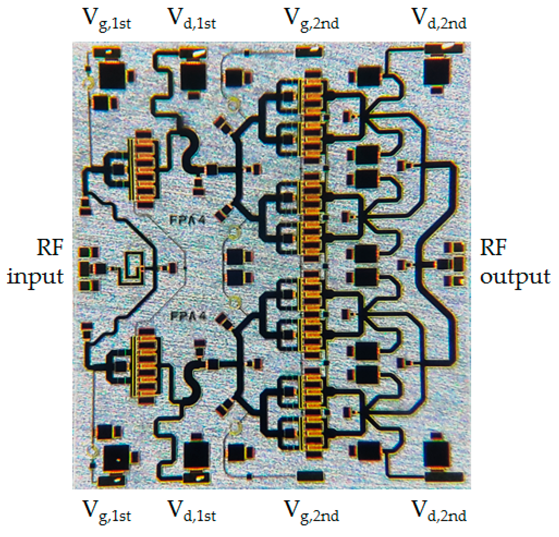
A chip photograph of the fabricated power amplifier MMIC is shown in Figure 10, and the chip size is 3.4 mm × 3.9 mm. The series and parallel inductors used in the circuit design are implemented using microstrip lines. Interstage and output matching circuits into which high drain DC current flows are designed using double-layered metal lines to withstand high current and minimize line loss. TaN resistors of 20 Ω are used between transistor cells to prevent plausible odd-mode oscillations that may be caused by a transistor imbalance of the corporate structure.
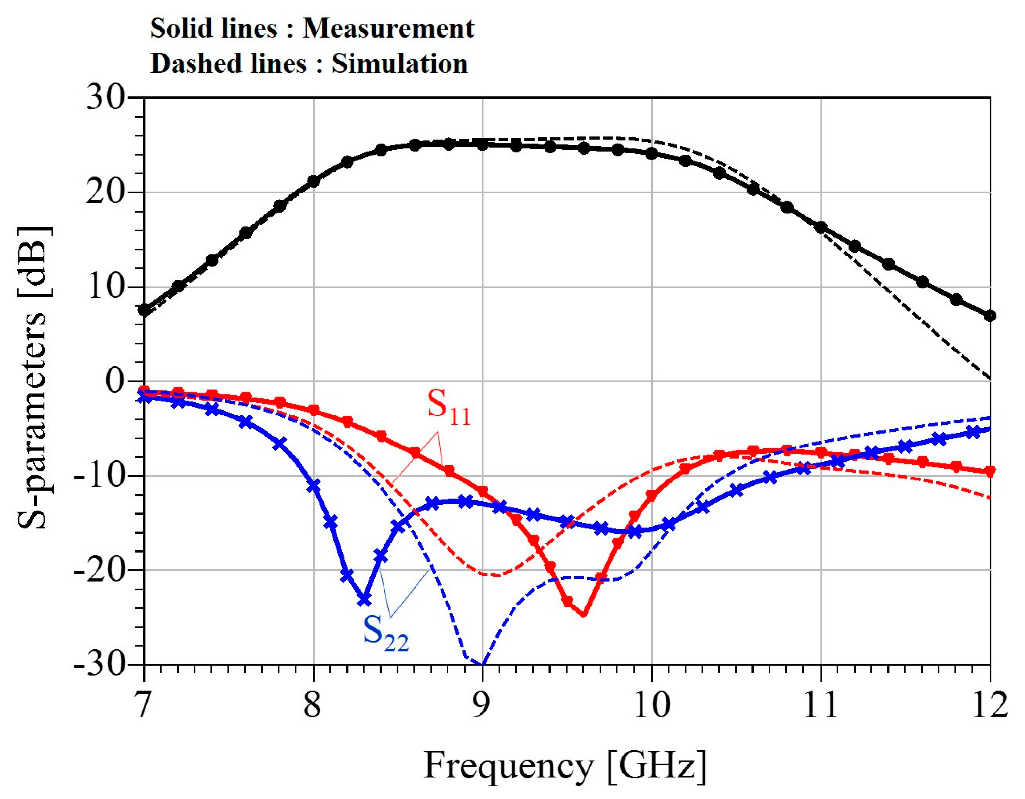
Figure 11 compares the measured S-parameter results with the simulated results at bias conditions of Vds = 28 V and Ids = 700 mA. The measured linear gain is 21.2 to 25.1 dB from 8.5 to 10.5 GHz and shows a tendency to gradually decrease within about 1 dB from 9.5 to 10.5 GHz. The input return loss is 7 dB or more at 8.5–10.5 GHz and 10 dB or more at 9–10 GHz, and the output return loss is 10 dB or more at 8.5–10.5 GHz.
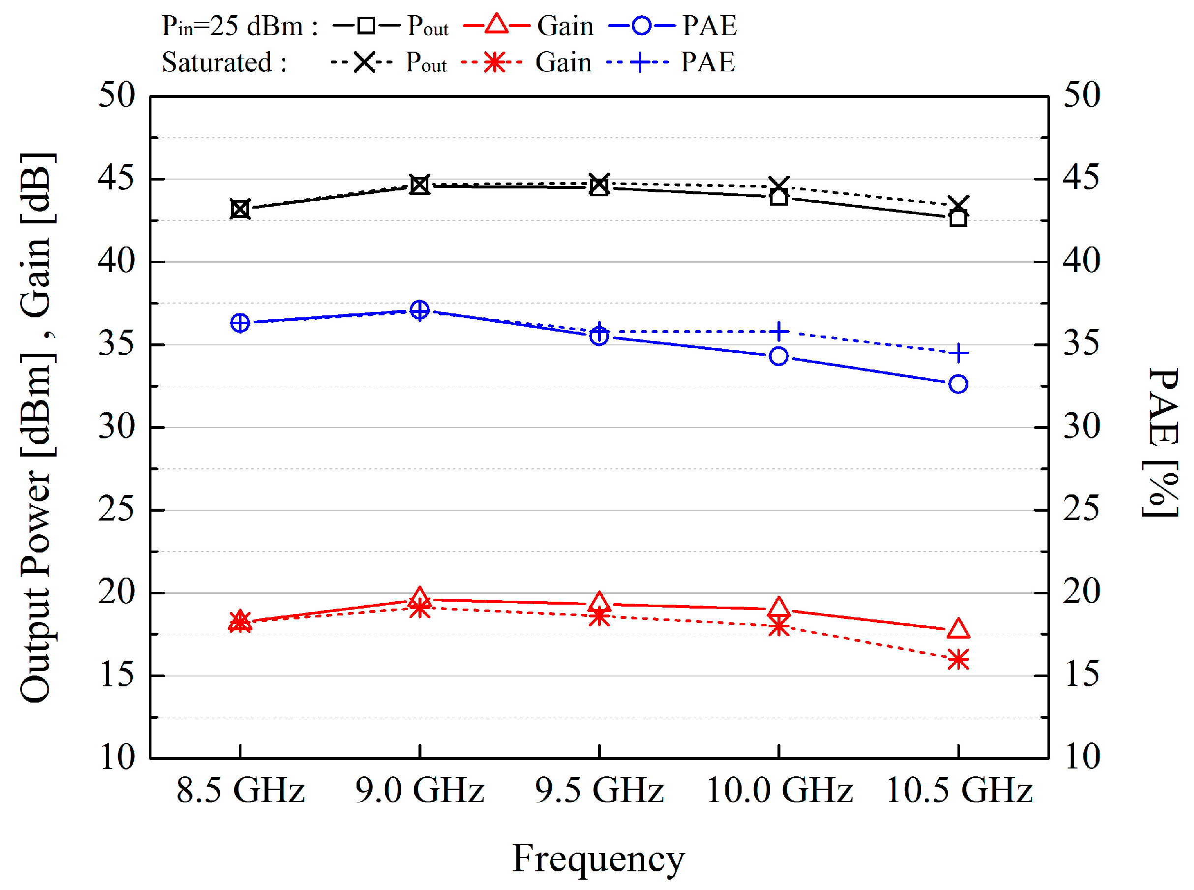
Figure 12 shows the measured output power, PAE, and power gain at Vds = 28 V and Ids = 1.2 A in a pulsed mode with a duty cycle of 10% and a pulse width of 100 μs. An output power of 43.2 to 44.6 dBm and a PAE of 33 to 37% are measured together with an associated gain of 17.7 to 19.6 dB at an available input power of 25 dBm in 8.5–10.5 GHz. The saturated output power is 43.2 to 44.7 dBm and at that condition the PAE is measured to be 35 to 37% with an associated gain of 16.0 to 19.1 dB in 8.5–10.5 GHz. At the saturated power condition, the output power increases by 0.3 to 0.7 dB and the PAE increases by 0.3 to 1.9% from 9.5 to 10.5 GHz. The output power is saturated below 9.5 GHz at the input power of 25 dBm, and a further increase of the input power seldom changes the output power and PAE. Figure 13 compares the measured power performance with the input power at 9.5 GHz with the simulated results. The measured PAE at the saturated output power condition is reduced by 5%, compared with the simulated results, and this is discussed in the next section.
We compared the results of our work with previously published state-of-the-art X-band GaN power amplifier MMIC results in Table 1. The comparison shows that our work is competitive in terms of the output power density and has reasonable performance over all.
5. Discussion
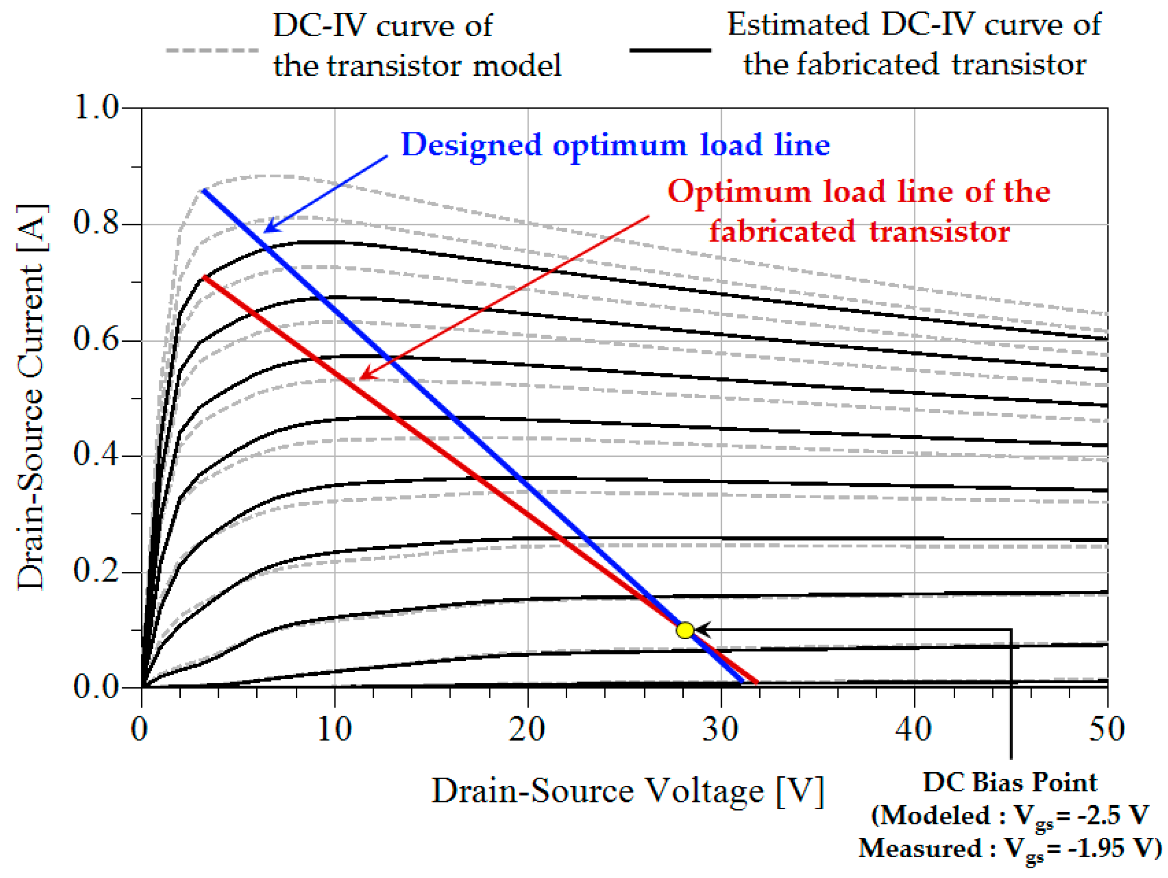
The measured PAE of the fabricated MMIC is reduced by about 5% compared with the PAE expected by the simulation. This is because the gate-source pinch-off voltage of the fabricated transistor shifts in a positive direction by about 0.5 V. The nonlinear transistor model provided by the foundry company has a pinch-off voltage of Vgs = −3.0 V at Vds = 28 V, but the fabricated transistor has a pinch-off voltage of Vgs = −2.5 V at Vds = 28 V. As shown in Figure 14, under a negative gate-source voltage range of 0 V to the pinch-off voltage, the fabricated transistor has a reduced drain current curve due to the pinch-off voltage shift, compared with the transistor model. Finally, the optimum load resistance of the fabricated transistor is larger than the designed load resistance, and the PAE hence decreases slightly because of the drain current clipping effect.
6. Conclusions
In this work, we presented an X-band GaN power amplifier MMIC that was developed using a 0.25 μm GaN HEMT foundry process of WIN semiconductors. The output matching circuit utilized an area-efficient corporate structure and was tuned at the third harmonic frequency for the PAE improvement. The input matching circuit was designed to have a low input VSWR while reducing the number of stages of the LC low-pass matching circuit through a simple lossy matching. The measured results of the fabricated power amplifier MMIC showed a linear gain of 20 dB or more, a saturated output power of 43.2 to 44.7 dBm, and a PAE of 35 to 37% from 8.5 to 10.5 GHz. If the transistor’s pinch-off voltage can be controlled more accurately, the developed power amplifier MMIC is expected to show very similar measured results to the simulated results. The developed MMIC chip could be effectively used for X-band radar system applications.
Author Contributions
Kyung-Tae Bae performed the circuit design and experiments and wrote the initial draft. Ik-Joon Lee contributed to the layout and EM simulations. Byungjoo Kang helped with the design rule check (DRC) of the layout and the measurement set-up, and Sanghoon Sim gave advice on the circuit design strategy. Laurence Jeon financially supported this work. Dong-Wook Kim supervised the whole process of this work, and fully reviewed and revised the draft.
Conflicts of Interest
The authors declare no conflict of interest.
References
- Brookner, E. Phased Array Radars-Past, Present and Future. In Proceedings of the 2002 RADAR, Edinburgh, UK, 15–17 October 2002; pp. 104–113. [Google Scholar]
- Ludwig, M.; Feldle, H.-P.; Ott, H. A Miniaturised X-Band T/R-Module for SAR-Systems Based on Active Phased Array Techniques. In Proceedings of the 1995 International Geoscience and Remote Sensing Symposium, Firenze, Italy, 10–14 July 1995; pp. 2063–2065. [Google Scholar]
- Lacomme, P. New Trends in Airborne Phased Array Radars. In Proceedings of the 2003 IEEE International Symposium on Phased Array Systems and Technology, Boston, MA, USA, 14–17 October 2003; pp. 17–22. [Google Scholar]
- Terry, E. Semiconductor Technology Trends for Phased Array Antenna Power Amplifiers. In Proceedings of the 2006 3rd European Radar Conference, Manchester, UK, 13–15 September 2006; pp. 269–272. [Google Scholar]
- Bettidi, A.; Cetronio, A.; Cicolani, M.; Costrini, C.; Lanzieri, C.; Maccaroni, S.; Marescialli, L.; Peroni, M.; Romanini, P. X-Band T/R Module in State-of-the-Art GaN Technology. In Proceedings of the 2009 European Radar Conference, Rome, Italy, 30 September–2 October 2009; pp. 258–261. [Google Scholar]
- Ortega-Gonzalez, F.-J.; Tena-Ramos, D.; Patiño-Gomez, M.; Pardo-Martin, J.M.; Madueño-Pulido, D. High-Power Wideband L-Band Suboptimum Class-E Power Amplifier. IEEE Trans. Microw. Theory Tech. 2013, 61, 3712–3720. [Google Scholar] [CrossRef]
- Liu, S.; Schreurs, D. Intrinsic Class-F RF GaN Power Amplifier with a Commercial Transistor Based on a Modified Hybrid Approach. In Proceedings of the 2012 Workshop on Integrated Nonlinear Microwave and Millimetre-wave Circuits, Dublin, Ireland, 3–4 September 2012. [Google Scholar]
- Rezaei, S.; Belostotski, L.; Ghannouchi, F.-M.; Aflaki, P. Integrated Design of a Class-J Power Amplifier. IEEE Trans. Microw. Theory Tech. 2013, 61, 1639–1648. [Google Scholar] [CrossRef]
- Piotrowicz, S.; Ouarch, Z.; Chartier, E.; Aubry, R.; Callet, G.; Floriot, D.; Jacquet, J.-C.; Jardel, O.; Morvan, E.; Reveyrand, T.; et al. 43W, 52% PAE X-Band AlGaN/GaN HEMTs MMIC Amplifiers. In Proceedings of the 2010 IEEE MTT-S International Microwave Symposium Digest, Anaheim, CA, USA, 23–28 May 2010; pp. 505–508. [Google Scholar]
- Kühn, J.; van Raay, F.; Quay, R.; Kiefer, R.; Maier, T.; Stibal, R.; Mikulla, M.; Seelmann-Eggebert, M.; Bronner, W.; Schlechtweg, M.; et al. Design of Highly-Efficient GaN X-Band Power Amplifier MMICs. In Proceedings of the 2009 IEEE MTT-S International Microwave Symposium Digest, Boston, MA, USA, 7–12 June 2009; pp. 661–664. [Google Scholar]
- Sardin, D.; Reveyrand, T.; Popović, Z. X-band 10 W MMIC High-Gain Power Amplifier with up to 60% PAE. In Proceedings of the 2014 9th European Microwave Integrated Circuit Conference, Rome, Italy, 6–7 October 2014; pp. 393–396. [Google Scholar]
- Resca, D.; Raffo, A.; Falco, S.-D.; Scappaviva, F.; Vadalà, V. X-Band GaN Power Amplifier for Future Generation SAR Systems. IEEE Microw. Wirel. Compon. Lett. 2014, 24, 266–268. [Google Scholar] [CrossRef]
- WIN Semiconductors Corp. Process Roadmap. Available online: http://www.winsemiconductorscorp.com (accessed on 1 July 2016).
- Lee, S.-K.; Bae, K.-T.; Kim, D.-W. 2–6 GHz GaN HEMT Power Amplifier MMIC with Bridged-T All-Pass Filters and Output-Reactance-Compensation Shorted Stubs. J. Semicond. Technol. Sci. 2016, 16, 312–318. [Google Scholar] [CrossRef]
- Costrini, C.; Cetronio, A.; Romanini, P.; Breglio, G.; Irace, A.; Riccio, M. 50W X-band GaN MMIC HPA: Effective Power Capability and Transient Thermal Analysis. In Proceedings of the 2010 40th European Microwave Conference, Paris, France, 28–30 September 2010; pp. 1650–1653. [Google Scholar]
- D’Angelo, S.; Biondi, A.; Scappaviva, F.; Resca, D.; Monaco, V.-A. A GaN MMIC Chipset Suitable for Integration in Future X-band Spaceborne Radar T/R Module Frontends. In Proceedings of the 2016 21st International Conference on Microwave, Radar and Wireless Communications (MIKON), Krakow, Poland, 9–11 May 2016. [Google Scholar]
- Shin, D.-H.; Yom, I.-B.; Kim, D.-W. X-Band GaN MMIC Power Amplifier for the SSPA of a SAR System. In Proceedings of the 2017 IEEE International Symposium on Radio-Frequency Integration Technology, Seoul, Korea, 30 August–1 September 2017; pp. 93–95. [Google Scholar]
- Wolfspeed, MMIC Bare Die, CMPA801B025D Data Sheet. Available online: http://www.wolfspeed.com (accessed on 1 October 2017).
- Qorvo, High Frequency Amplifiers, TGA2624 Data Sheet. Available online: http://www.qorvo.com (accessed on 1 October 2017).
Figure 1.
Transistor with a parallel RC circuit at the gate for the unconditional stability.

Figure 2.
Load-pull simulation results of the stabilized 6 × 150 μm and 10 × 150 μm HEMTs at 9.5 GHz: output power and PAE contours of (a) the 6 × 150 μm; and (b) 10 × 150 μm.
Figure 2.
Load-pull simulation results of the stabilized 6 × 150 μm and 10 × 150 μm HEMTs at 9.5 GHz: output power and PAE contours of (a) the 6 × 150 μm; and (b) 10 × 150 μm.
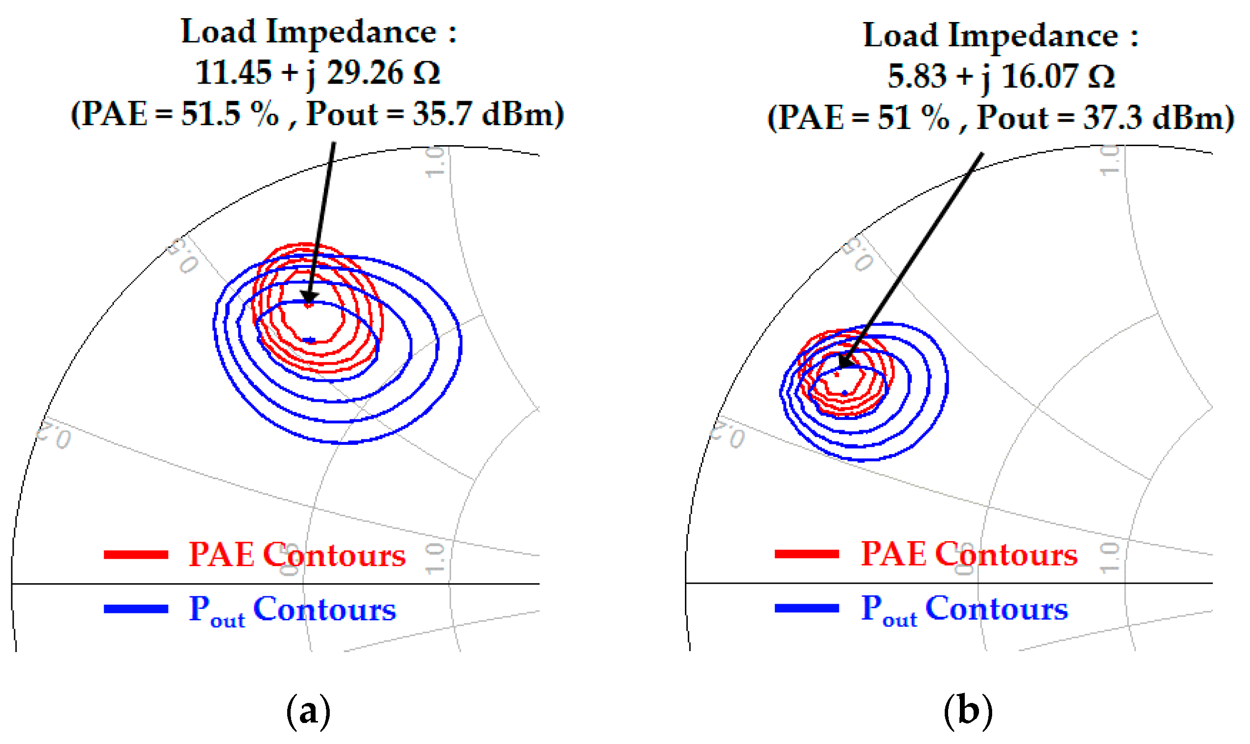
Figure 3.
Schematic circuit diagram of the X-band high-power amplifier MMIC.
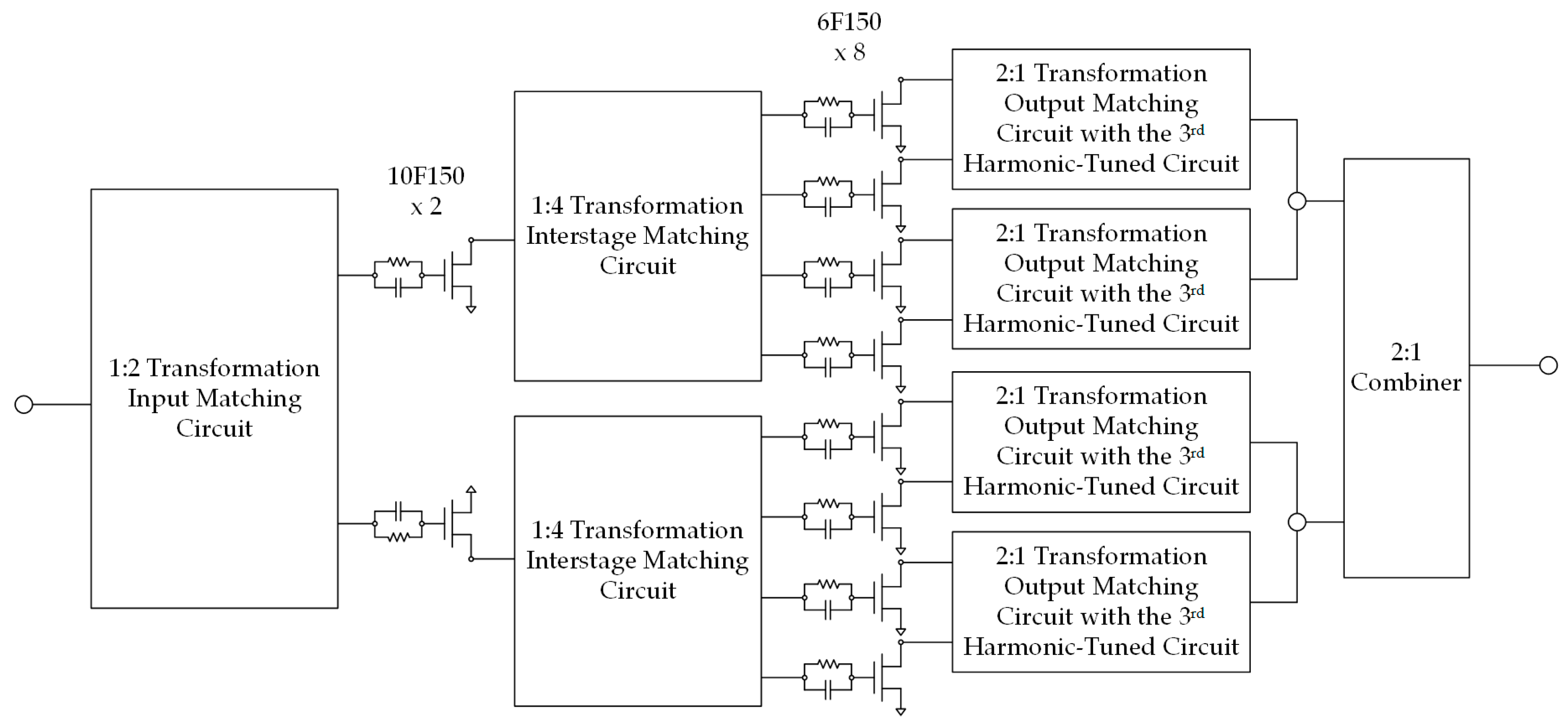
Figure 4.
Simplified output equivalent circuit model of the transistor that illustrates a current generator plane and an extrinsic device plane.
Figure 4.
Simplified output equivalent circuit model of the transistor that illustrates a current generator plane and an extrinsic device plane.

Figure 5.
Harmonic load-pull simulation results of a 6 × 150 μm HEMT at the device’s extrinsic plane at the bias conditions of Vds = 28 V and Ids = 100 mA/mm where the fundamental frequency is 9.5 GHz: (a) Load impedance contours at the second harmonic frequency (f0: optimal, 3f0: open); (b) Load impedance contours at the third harmonic frequency (f0: optimal, 2f0: open).
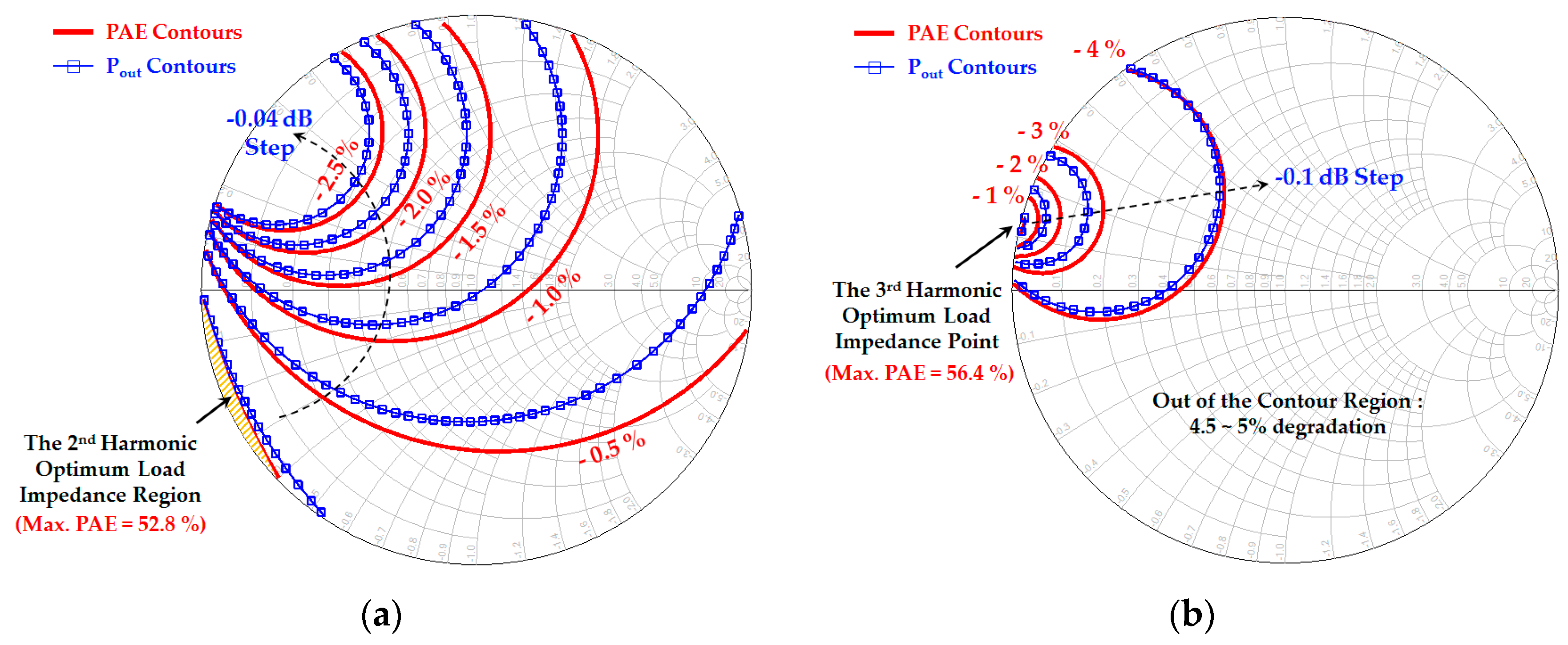
Figure 6.
Output matching circuit that performs optimum impedance matching at the fundamental frequency and the third harmonic impedance tuning for two 6 × 150 μm HEMTs.
Figure 6.
Output matching circuit that performs optimum impedance matching at the fundamental frequency and the third harmonic impedance tuning for two 6 × 150 μm HEMTs.

Figure 7.
The loci of the load impedance Zopt that is the impedance of the output matching circuit seen from the transistor.
Figure 7.
The loci of the load impedance Zopt that is the impedance of the output matching circuit seen from the transistor.
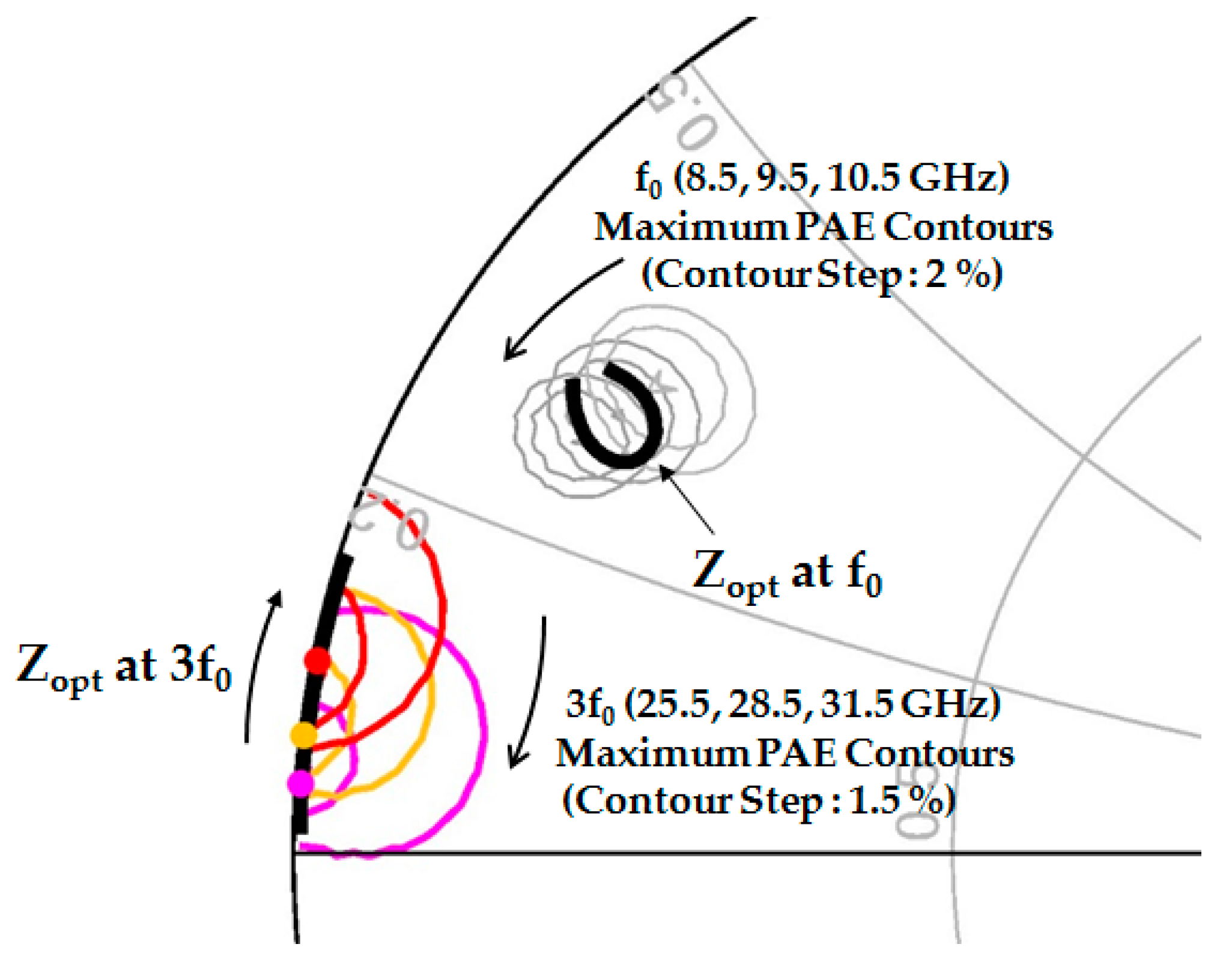
Figure 8.
Lossy input matching circuit with LC low-pass filters and a shunt R-C circuit.

Figure 9.
Simulated results of the lossy input matching circuit with the shunt resistor Rs: (a) Input return loss; (b) Insertion loss.
Figure 9.
Simulated results of the lossy input matching circuit with the shunt resistor Rs: (a) Input return loss; (b) Insertion loss.

Figure 10.
Photograph of the fabricated X-band GaN power amplifier MMIC. The chip occupies an area of 3.4 mm × 3.9 mm (13.26 mm2).
Figure 10.
Photograph of the fabricated X-band GaN power amplifier MMIC. The chip occupies an area of 3.4 mm × 3.9 mm (13.26 mm2).

Figure 11.
Comparison of simulated and measured S-parameter results of the fabricated power amplifier MMIC at the bias conditions of Vds = 28 V and Ids = 700 mA.
Figure 11.
Comparison of simulated and measured S-parameter results of the fabricated power amplifier MMIC at the bias conditions of Vds = 28 V and Ids = 700 mA.

Figure 12.
Measured output power, power gain, and power-added efficiency of the fabricated power amplifier MMIC at Pin = 25 dBm and the input power condition for the saturated output power. The bias conditions are Vds = 28 V and Ids = 1.2 A, and the measurement is done under pulsed conditions with a pulse width of 100 μs and a duty cycle of 10%.

Figure 13.
Simulated and measured power performance of the fabricated power amplifier MMIC with input power at 9.5 GHz.
Figure 13.
Simulated and measured power performance of the fabricated power amplifier MMIC with input power at 9.5 GHz.
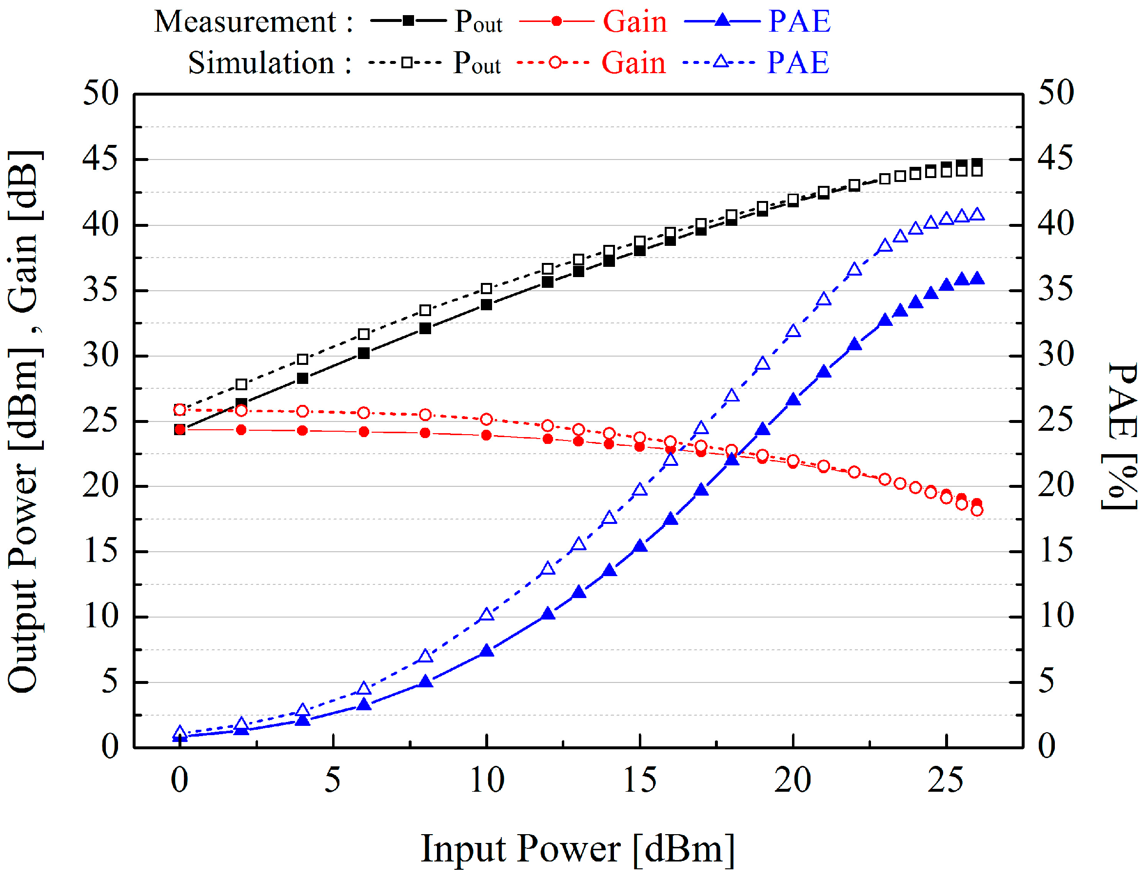
Figure 14.
DC-IV curves and optimum load lines of the fabricated transistor and the nonlinear transistor model (Vgs = −3.6 to 0 V, voltage step = 0.3 V).
Figure 14.
DC-IV curves and optimum load lines of the fabricated transistor and the nonlinear transistor model (Vgs = −3.6 to 0 V, voltage step = 0.3 V).


Table 1.
Summary and comparison of our work and previously published state-of-the-art X-band GaN power amplifier MMIC results.
Table 1.
Summary and comparison of our work and previously published state-of-the-art X-band GaN power amplifier MMIC results.
| Reference | Technology | Frequency (GHz) | Pulse Width/Duty (μs/%) | Vds (V) | Pout (W) | PAE (%) | Area (mm2) | Power Density (W/mm2) |
|---|---|---|---|---|---|---|---|---|
| [9] | 0.25 μm GaN | 8.5–11.0 | 20/10 | 25 | 25–43 | 33–52 | 18 | 2.89 |
| [10] | 0.25 μm GaN | 8.5–10.5 | 100/10 | 30 | 17–19 | 32–35 | 13.5 | 1.41 |
| [11] | 0.25 μm GaN | 10.0–10.5 | CW | 25 | 10–14 | 45–61 | 9.2 | 1.52 |
| [12] | 0.25 μm GaN | 8.6–10.6 | 50/15 | 26 | 12–15 | 38–43 | 18 | 0.83 |
| [15] | 0.5 μm GaN | 8.0–10.5 | 10/1 | 35 | 50–57 | 27–32 | 16 | 3.56 |
| [16] | 0.25 μm GaN | 8.8–10.2 | 100/30 | 30 | 28–32 | 36–37 | 22 | 1.45 |
| [17] | 0.25 μm GaN | 8.8–10.8 | 100/10 | 28 | 30–40 | 38–44 | 20.7 | 1.93 |
| [18] | 0.25 μm GaN | 8.0–11.0 | 100/10 | 28 | 32–47 | 37–44 | 17.28 | 2.72 |
| [19] | 0.25 μm GaN | 9.0–10.5 | 100/10 | 28 | 18–20 | 40–43 | 13 | 1.54 |
| This Work | 0.25 μm GaN | 8.5–10.5 | 100/10 | 28 | 21–29 | 35–37 | 13.26 | 2.19 |
© 2017 by the authors. Licensee MDPI, Basel, Switzerland. This article is an open access article distributed under the terms and conditions of the Creative Commons Attribution (CC BY) license (http://creativecommons.org/licenses/by/4.0/).
Share and Cite
MDPI and ACS Style
Bae, K.-T.; Lee, I.-J.; Kang, B.; Sim, S.; Jeon, L.; Kim, D.-W. X-Band GaN Power Amplifier MMIC with a Third Harmonic-Tuned Circuit. Electronics 2017, 6, 103. https://doi.org/10.3390/electronics6040103
AMA Style
Bae K-T, Lee I-J, Kang B, Sim S, Jeon L, Kim D-W. X-Band GaN Power Amplifier MMIC with a Third Harmonic-Tuned Circuit. Electronics. 2017; 6(4):103. https://doi.org/10.3390/electronics6040103
Chicago/Turabian StyleBae, Kyung-Tae, Ik-Joon Lee, Byungjoo Kang, Sanghoon Sim, Laurence Jeon, and Dong-Wook Kim. 2017. "X-Band GaN Power Amplifier MMIC with a Third Harmonic-Tuned Circuit" Electronics 6, no. 4: 103. https://doi.org/10.3390/electronics6040103
Note that from the first issue of 2016, this journal uses article numbers instead of page numbers. See further details here.