1. Introduction
Printed electronics are attracting research interest because they have many advantages, such as ease of manufacturing (using solution-based materials and an adaptable roll-to-roll process), low cost, and eco-friendly processing [
1,
2,
3,
4]. There have been many attempts to fabricate electronic devices using printing techniques, including organic photovoltaic cells [
5], organic thin film transistors [
6], radio frequency identification tags [
7], organic light emitting diodes [
8], and printing-based sensors [
9].
Such printed devices typically have a multi-layer structure, called a “sandwich structure”. Each layer in multi-layer devices consists of a different material that depends on its function. For example, a conductive layer may use Ag or Cu, an insulating layer may use polymethyl methacrylate (PMMA), BaTiO
3, or Epoxy, and a semiconducting layer may use poly-3-hexylthiophene-2,5-diyl: phenyl-C61-butyric acid methyl ester (P3HT:PCBM) or triisopropylsilyl (TIPS) pentacene [
10,
11,
12,
13]. Each functional layer shows various characteristics, and the device types are determined when the layers are overlaid in different sequences in the multi-layer structure. The main performance parameters measured include the electrical resistivity of conductive patterns, the permittivity of the dielectric layer, the mobility of the semiconducting layer, and mechanical properties, such as the thickness and roughness of the printed surface [
14,
15,
16].
The chemical properties of solutions can be enhanced by changing the synthesis methods and materials, but the mechanical properties depend on the printing technique, which determines the morphology of the surface. In particular, the morphology of a printed layer changes rapidly when the multi-layer structure is printed. Specifically, thickness variations accumulate as printed layers are added. Furthermore, the morphology at the interface in a multi-layer structure can be changed by the dissolution caused by the solvent in the ink that occurs at the interface between the printed layers. A rough printed surface can also affect the performance and reliability of the device [
17,
18].
In this study, a parallel-plate capacitor was selected as an example device to observe the interfacial phenomena that affect the device performance. A printed capacitor has a simple multi-layer structure that sequentially overlaps the substrate with a conductive layer, a dielectric, and another conductive layer. Previous studies have used many fabrication techniques, such as screen printing, inkjet printing, and gravure printing [
19,
20,
21] to fabricate printed capacitors. The spin printing process, which guarantees good uniformity, was used to make the printed capacitor devices for this study. In order to investigate the influence of various parameters on the coating quality and capacitance of the multi-layer structure, the capacitors were printed using two kind types of commercial Ag conductive ink, each of which has different material particle sizes and vehicle solvent. The printed capacitors were then analyzed and compared using both theoretical and experimental approaches. To observe the functionality, the printed capacitors were configured in a low-pass filter (LPF) implementation. Correlations between the process conditions and functionality were discussed.
2. Experimental Section
2.1. Materials and Method
Borosilicate glass substrate, 30 mm × 30 mm in size, was cleaned with acetone, isopropyl alcohol (IPA), and distilled water, and dried with N2 gas. For the bottom plate, a conductive layer (the first layer) was spun at 4000 rpm for 10 s using two types of commercial Ag conductive ink (FLT-710GO, FP Co., Korea and PG-007, Paru Co., Busan, Korea) onto the glass substrate, followed by drying in a convection oven at 95 °C for 5 min. A commercial dielectric ink (PD-100, Paru Co., Suncheon, Korea) that has a permittivity of 121 pF/m was used to fabricate the second layer. The spin speeds of the second layer were 3000, 4000, and 5000 rpm for 10 s, followed by drying in a conduction oven at 95 °C for 5 min. The top plate (the third layer) was printed using the same process and parameters as for the first layer.
When the inks were spun, a polyimide (PI) film patterned by a cutting plotter (Craft ROBO CC330-20, Graphtec Co., Yokohama, Japan) was placed on the substrate and played the role of mask shown in
Figure 1. After spin-coating, PI mask was detached.
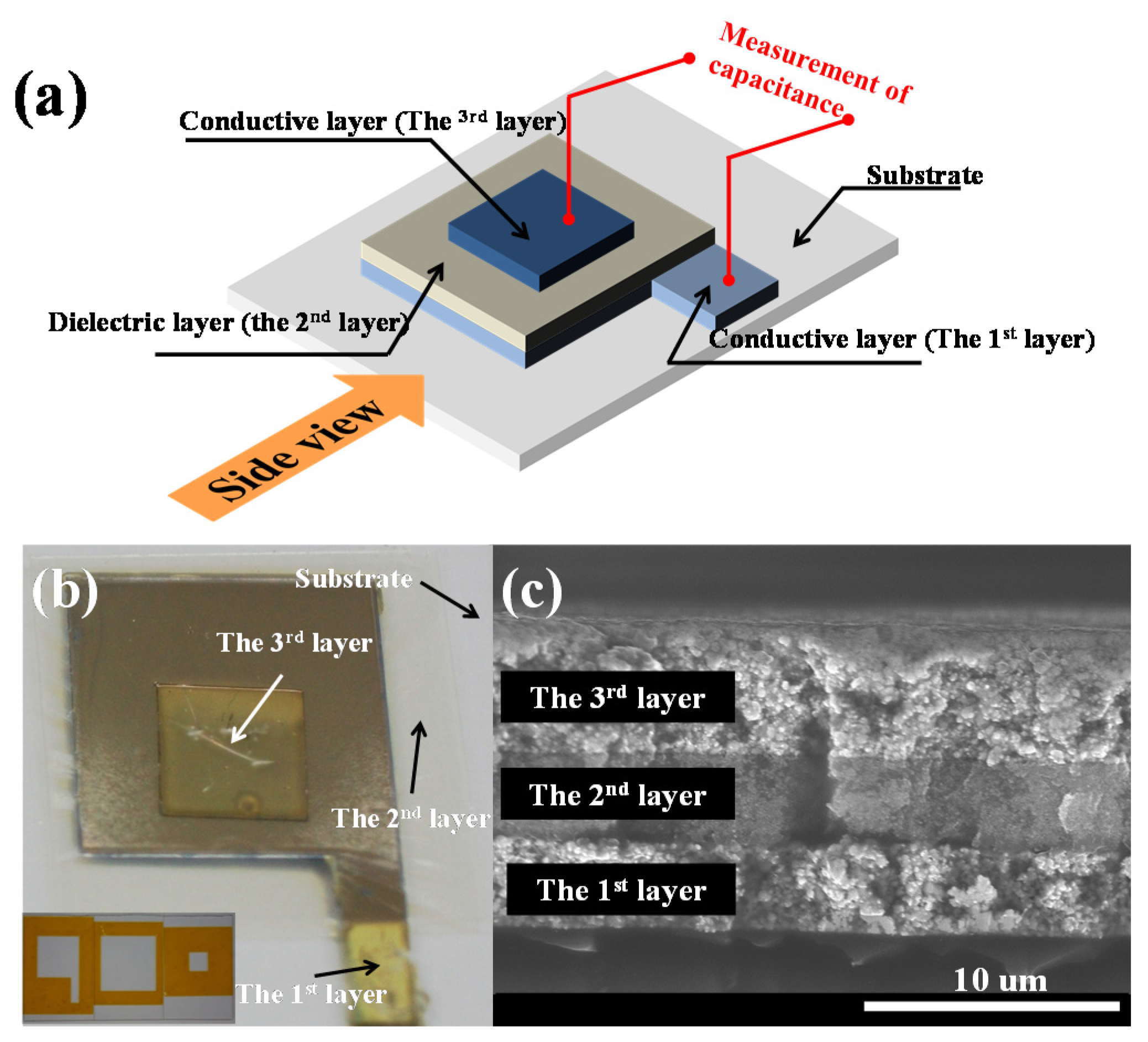
Figure 1.
Printed parallel-plate capacitor: (a) 3D schematics; (b) optical image (inset is polyimide masks for patterning); and (c) cross-sectional SEM image.
Figure 1.
Printed parallel-plate capacitor: (a) 3D schematics; (b) optical image (inset is polyimide masks for patterning); and (c) cross-sectional SEM image.
2.2. Measurement
In order to measure the printability and functionality of the printed parallel-plate capacitors, the surface morphology, thickness, and roughness of the printed conductive and dielectric layers were characterized using an optical microscope (ECLIPSE LV100ND, Nikon Ins. Co., Tokyo, Japan), a field emission scanning electron microscope (FESEM, S-4800, Hitachi Co., Tokyo, Japan), and an interferometer (NV-2000, Nano System Co., Daejeon, Korea), respectively. The contact angles of dielectric inks used as the second layer on top of two kinds of the first conductive layers were measured using a contact angle meter (GSA, Surface Tech., Gyeonggi, Korea). The capacitance of the fabricated capacitors was measured using a digital multimeter (UT70D, UNI-Trend Co., Hong Kong, China).
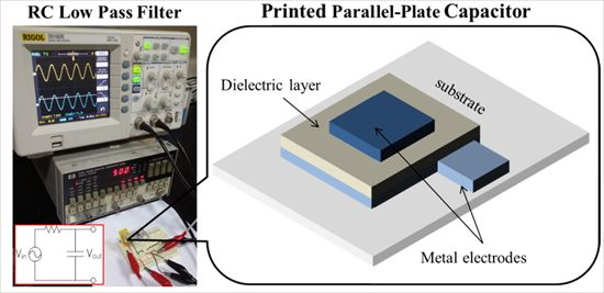
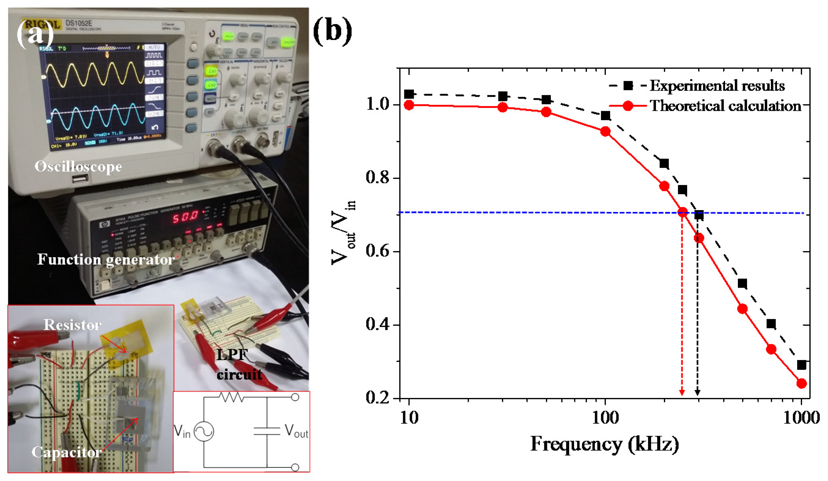
A resistor-capacitor low pass filter (RC LPF) was built using a printed resistor on a PI substrate and a fabricated capacitor on a glass substrate. The LPF circuit was constructed on a breadboard with electrical wiring. An alternating current (AC) signal was supplied by a function generator (8116A, Hewlett-Packard, Palo Alto, CA, USA), and the input and output voltages were measured using a digital oscilloscope (DS1052E, RIGOL Co., Beijing, China). The cutoff frequency and input-output ratio were first theoretically calculated and then verified by experiment.
3. Results and Discussion
The parallel-plate capacitor fabricated in this study is demonstrated in
Figure 1. As shown in
Figure 1a, the capacitor consisted of three layers (conductive-dielectric-conductive), each with a defined area and thickness. The first layer had an area of 100 mm
2 with a contact line for measuring capacitance. The second layer covered the first layer completely, excluding the contact line. Finally, the third layer acted as the top plate, and was spun onto the second layer with an area of 49 mm
2. An optical image of the printed capacitor is shown in
Figure 1b. The thickness of the dielectric layer was inspected by cross-sectional SEM, as shown in
Figure 1c, and was found to be 4.41, 4.16, and 2.97 μm when the spinning speed was 3000, 4000, and 5000 RPM, respectively.
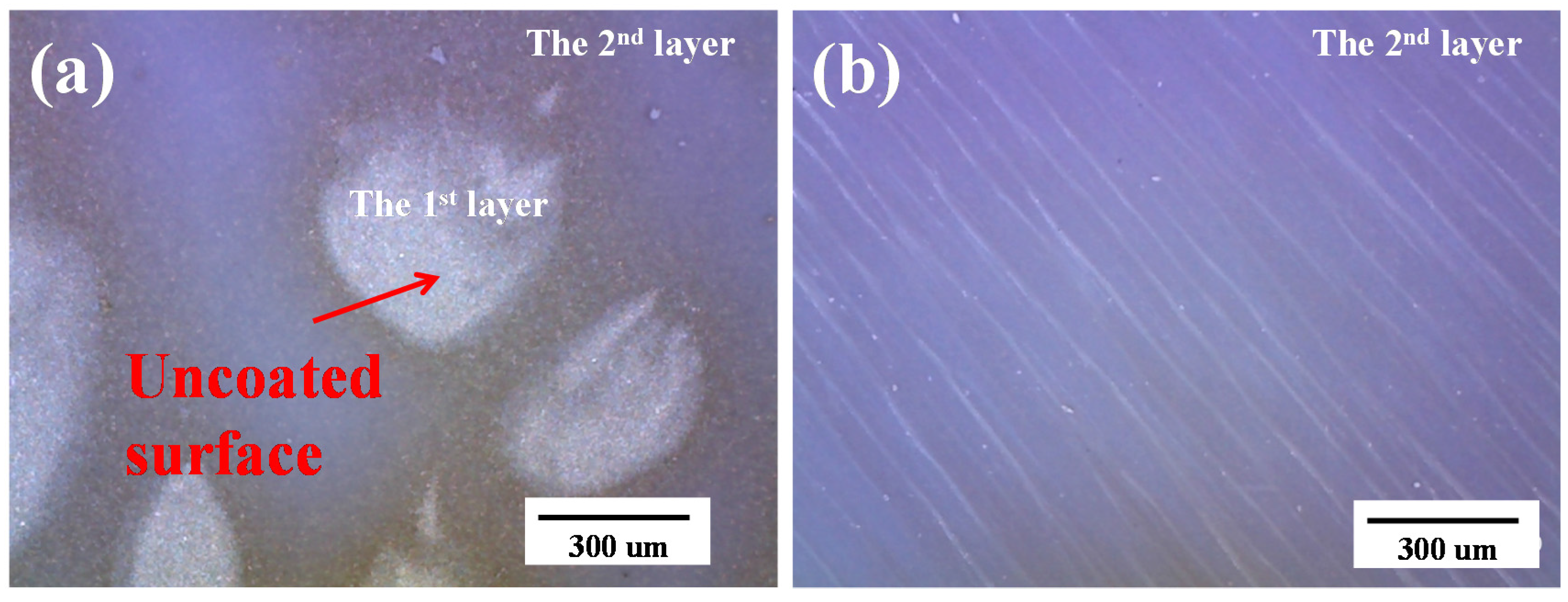
The surface morphology of the second layer was characterized using optical microscopy, and was found to be dependent on the first layer. As shown in optical images of
Figure 2, the dielectric layer did not perfectly cover the underlying layer when FLT-710GO was used as the first layer, while it did fully cover the first layer when PG-007 was used. The uncoated surface shown in
Figure 2a played the role of charge carrier conduction between the top and bottom plates, meaning the failure as a capacitor.
Figure 2.
Optical images of the second layer when the first layer was (a) FLT-710GO and (b) PG-007.
Figure 2.
Optical images of the second layer when the first layer was (a) FLT-710GO and (b) PG-007.
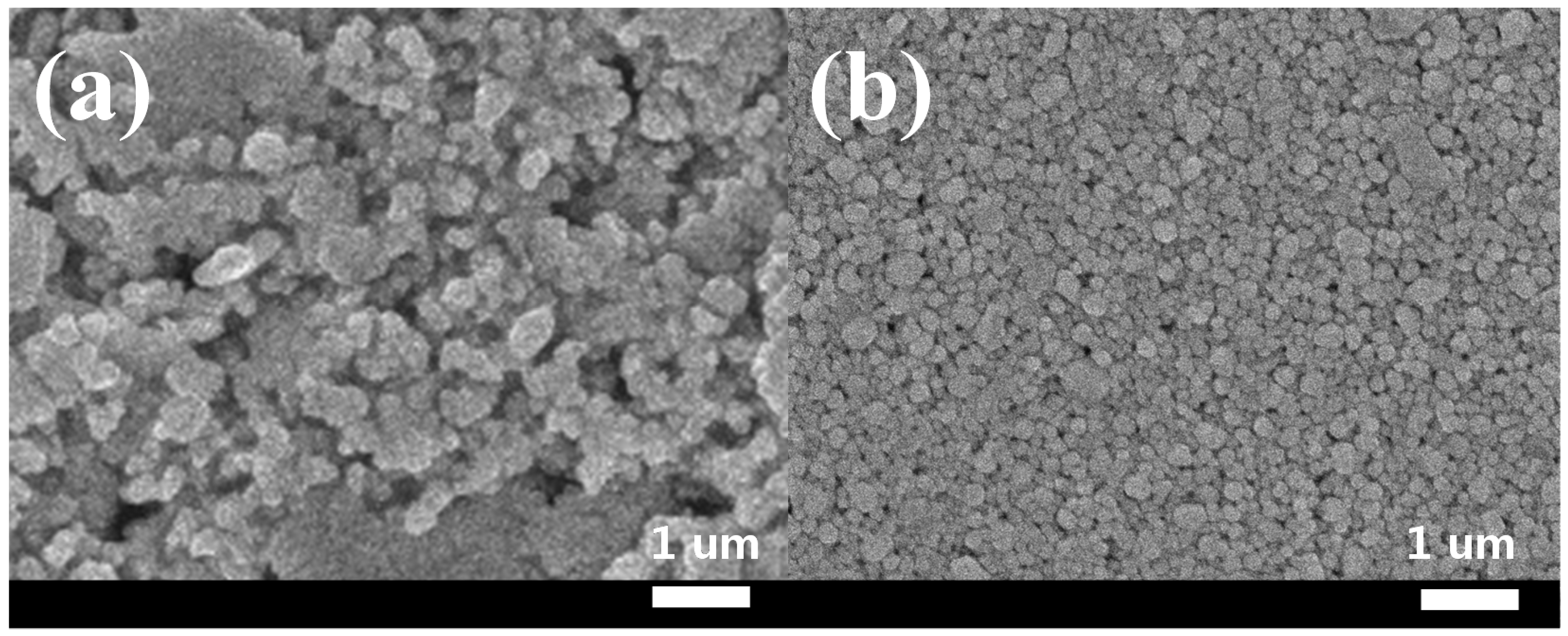
Figure 3 depicts SEM images of the first layer with FLT-710GO and PG-007. The sizes of the silver particles in
Figure 3a,b were about 1000 nm and 70 nm, respectively. In addition, aggregations of silver particles larger than several micrometers were observed, and these affected the quality of the subsequent dielectric layers. When the particle sizes were smaller and there was no aggregation, the layers could be stacked more densely, which reduced surface waviness and roughness, and lead to good quality subsequent layers. Furthermore, it is known that the contact angle on the surface increases when the roughness becomes high [
22]. The root mean square (RMS) roughness of the first layer was measured to be 153 nm and 9.53 nm for FLT-710GO and PG-007, respectively. The measured contact angle of the dielectric ink on the first layer for FLT-710GO and PG-007 was 65.1° and 50.8°, respectively. Both the existence of aggregations and the wettability influenced the fabrication of the stable thin film second layer on top of the first layer. For this reason, PG-007 conductive ink was used to construct the bottom plate in all of the parallel-plate capacitors. However, two types of conductive ink were still used to fabricate the top plates.
Figure 3.
SEM images of bottom plate composed of silver particles using (a) FLT-710GO and (b) PG-007.
Figure 3.
SEM images of bottom plate composed of silver particles using (a) FLT-710GO and (b) PG-007.
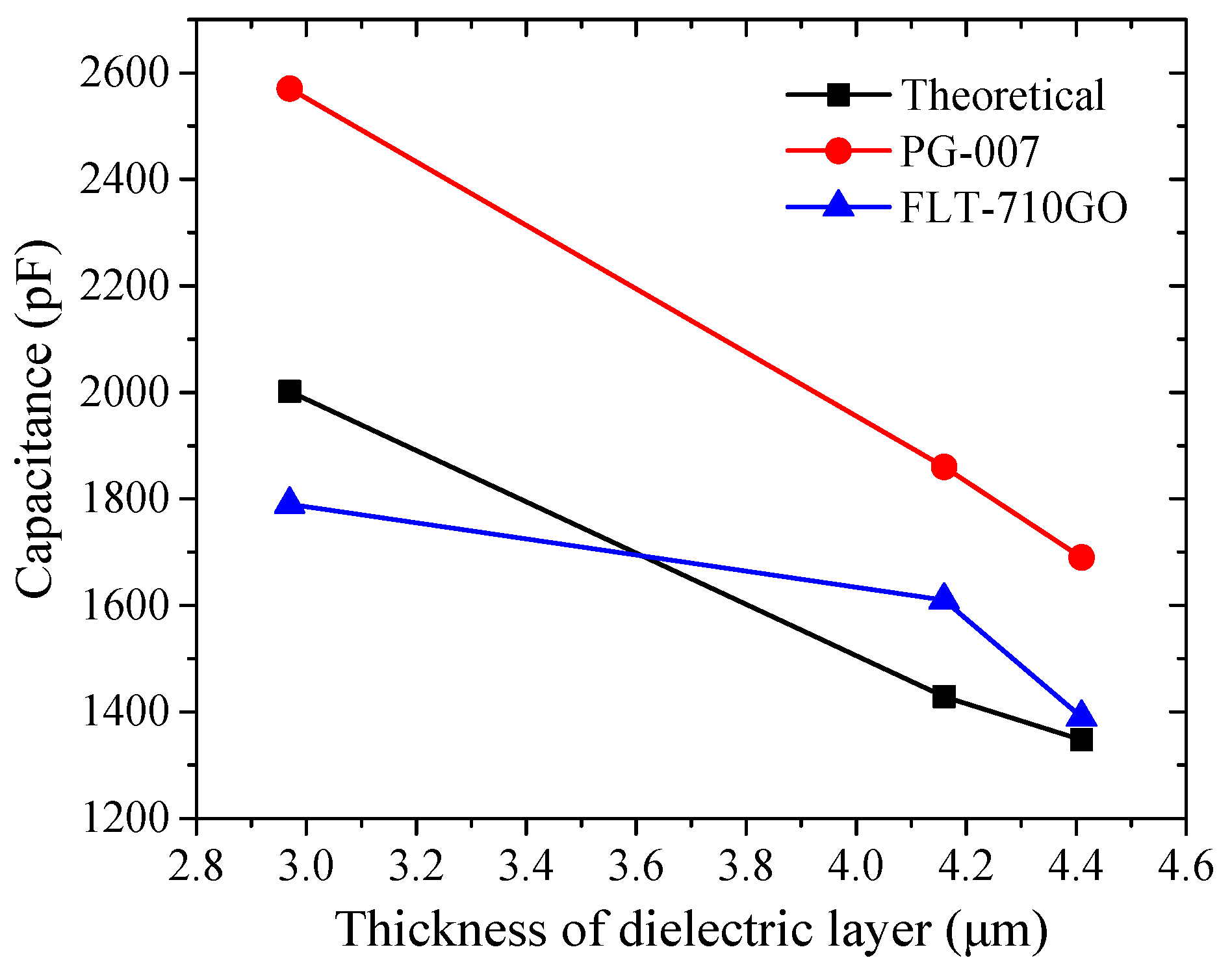
The measured and theoretical capacitances (
C) of the fabricated parallel-plate capacitors are shown in
Figure 4. The theoretical capacitance was obtained from Equation (1).
where ε represents permittivity; and
A and
t are geometric parameters that represent the area and thickness, respectively, of the dielectric layer.
Figure 4.
Theoretical and measured capacitance of fabricated parallel-plate capacitors versus the thickness of the dielectric layer.
Figure 4.
Theoretical and measured capacitance of fabricated parallel-plate capacitors versus the thickness of the dielectric layer.
As shown in
Figure 4, the capacitance decreases as the thickness of the dielectric layer increases, which is consistent with Equation (1). In particular, the capacitor that used PG-007 as the top plate exhibited an inverse linear relationship to the thickness. It should be noted that the experimental values are a bit higher than the theoretical calculation. This might be caused by the penetration of silver particles into the dielectric layer whose particle size was around 40 nm, which reduces the effective thickness of the layer and results in higher capacitance. In addition, the uneven boundary between the layers tends to concentrate the charges, which also increases the capacitance. In contrast, the capacitor that used FLT-710GO as the top plate showed capacitance that was close to the theoretical calculation and lower than the capacitors that used PG-007 as a top plate. Particles from the top plates did not penetrate into the dielectric layers because the particles were large and many formed aggregations. Another possible cause for the differences in capacitance is the effect of the vehicle solvent used in each ink. The solvent used in the FLT-710GO, PG-007, and PD-100 inks is dibutyl diglycol (C
4H
9O-(CH
2CH
2O)
2-C
4H
9) (solubility in water: 6.5%), ethylene glycol (HOCH
2CH
2OH) (solubility in water: 100%), and diethylene glycol monoethyl ether acetate (C
2H
5OCH
2CH
2OCH
2CH
2CO
2CH
3) (solubility in water: 100%), respectively. The polarity of the solvent in the FLT-710GO ink is farther away from that in the PD-100 ink than polarity of solvent in PG-007 ink. It means that the possibility of silver particles in the top plate percolating into the dielectric layer via the solvent is high when PG-007 is used.
An RC LPF was implemented using both printed resistors and capacitors employing PG-007, as shown in
Figure 5.
Figure 5a shows the measurement setup for the RC LPF circuit. Based on the measured values of 420 Ω and 1530 pF,
Figure 5b shows a comparison of the theoretical and experimental values for the input-output voltage ratio. The theoretical values for the input-output voltage ratio and the cutoff frequency were calculated using Equations (2) and (3), respectively [
23].
where
R and
C are the resistance and capacitance of the passive elements, respectively, and
V and ω are the voltage and frequency of the applied AC signals. The voltage ratio decreases gradually as the frequency increases for all frequencies below the cut-off frequency, which is the behavior of a conventional LPF. The actual cutoff frequency was measured to be 295 kHz, and is comparable to the calculated cutoff frequency of 247 kHz.
Figure 5.
Implementation of an resistor-capacitor low pass filter( RC LPF) using printed resistors and printed parallel-plate capacitors: (a) experimental set-up for measurements (inset: the wiring and schematic of the circuit); and (b) the input-output voltage ratio in the case where the printed capacitor used PG-007 as the top plate.


