
On the Stability and Electronic Structure of Transition-Metal Dichalcogenide Monolayer Alloys Mo1−xXxS2−ySey with X = W, Nb

Abstract
:
1. Introduction
2. Methods Section
3. Results and Discussion
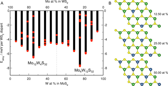
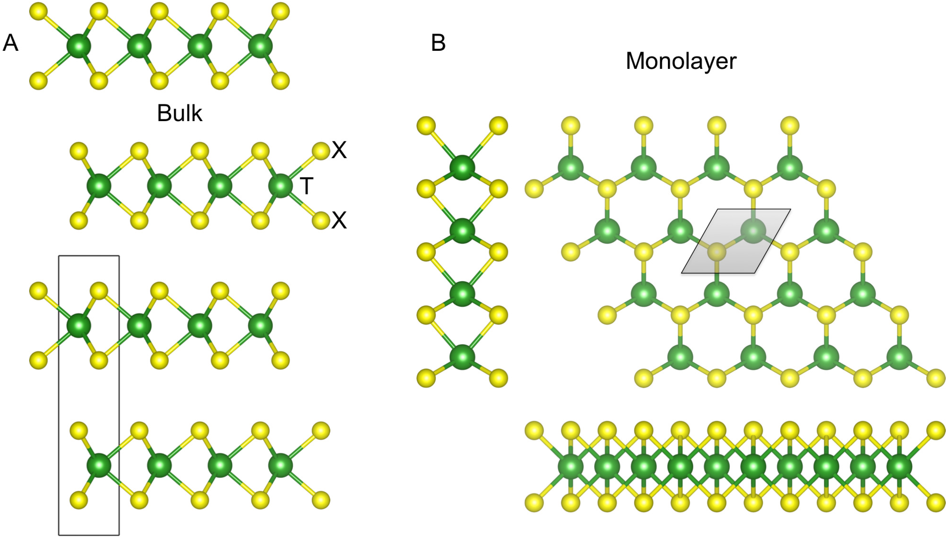
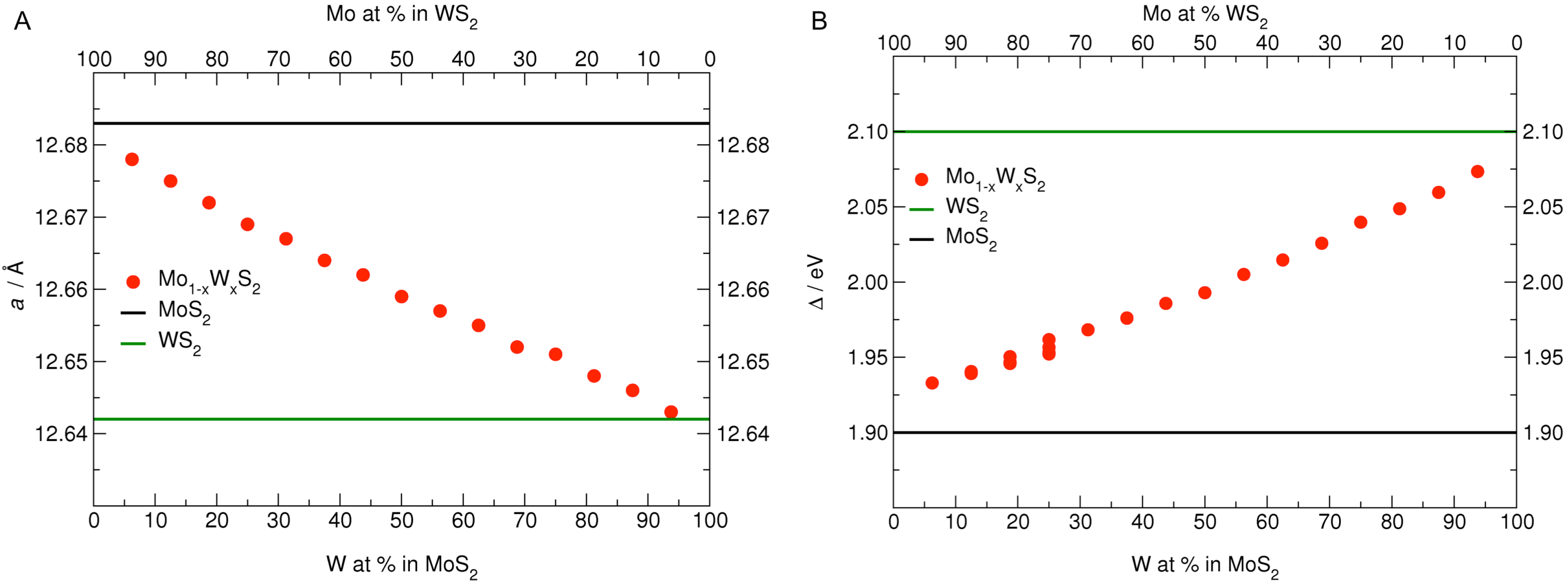
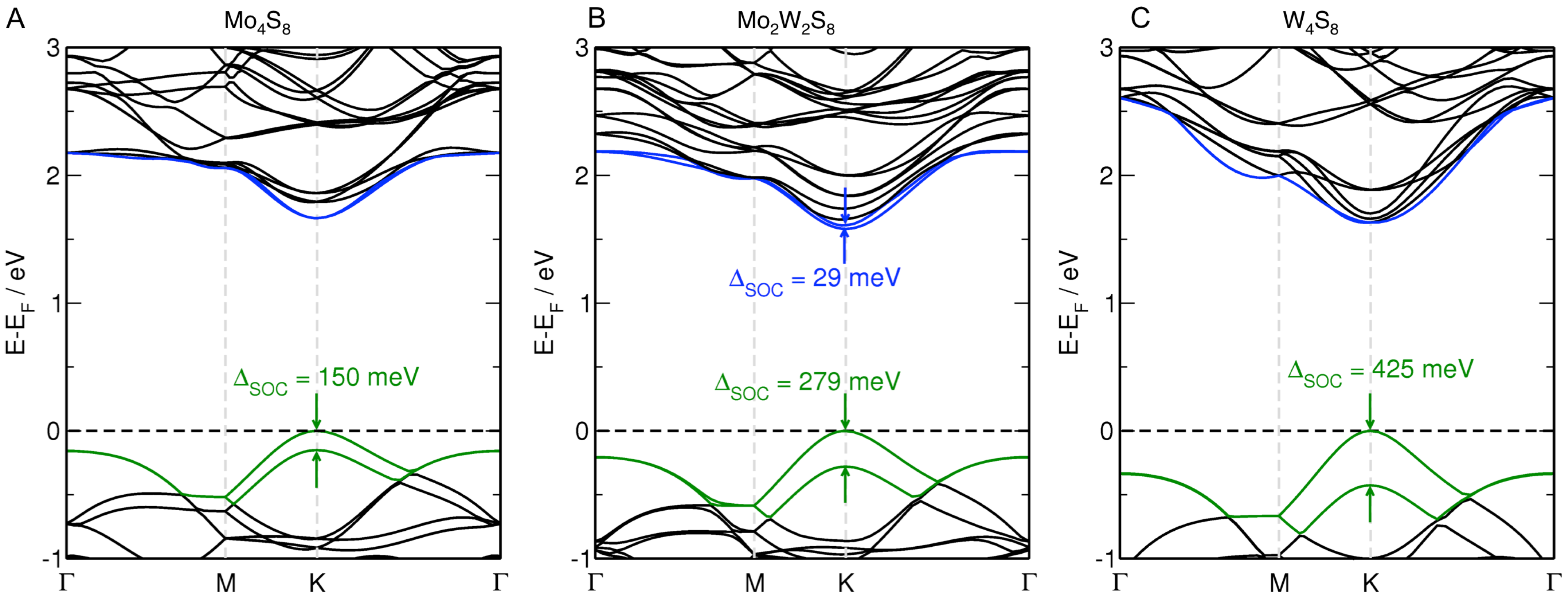
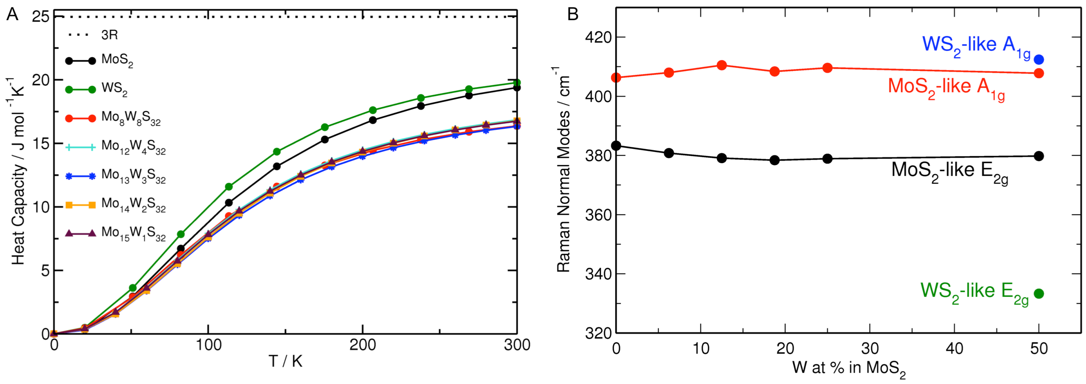
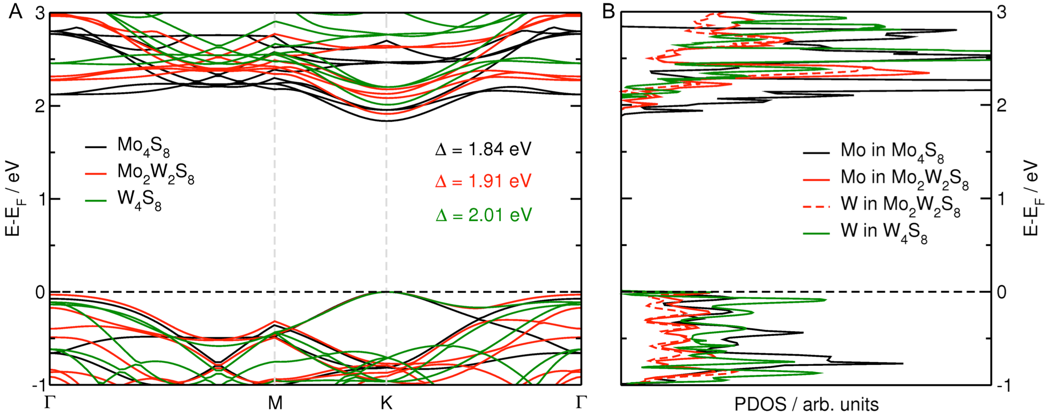
3.1. MoS Alloys with W

| Formula | W at% | a, b | W–W | Formula | Mo at% | a, b | Mo–Mo |
|---|---|---|---|---|---|---|---|
| MoS | 0.00 | 12.683 (12.656) | – | WS | 0.00 | 12.642 (12.616) | – |
| MoWS | 6.25 | 12.678 | – | MoWS | 6.25 | 12.643 | – |
| MoWS | 12.50 | 12.675 | 6.333 | MoWS | 12.50 | 12.646 | 6.322 |
| MoWS | 18.75 | 12.672 | 6.334 | MoWS | 18.75 | 12.648 | 6.322 |
| MoWS | 25.00 | 12.669 | 6.334 | MoWS | 25.00 | 12.651 | 6.325 |
| MoWS | 31.25 | 12.667 | 3.167 | MoWS | 31.25 | 12.652 | 3.163 |
| MoWS | 37.50 | 12.664 | 3.166 | MoWS | 37.50 | 12.655 | 3.164 |
| MoWS | 43.75 | 12.662 | 3.166 | MoWS | 43.75 | 12.657 | 3.164 |
| MoWS | 50.00 | 12.659 | 3.165 | MoWS | 50.00 | 12.659 | 3.165 |


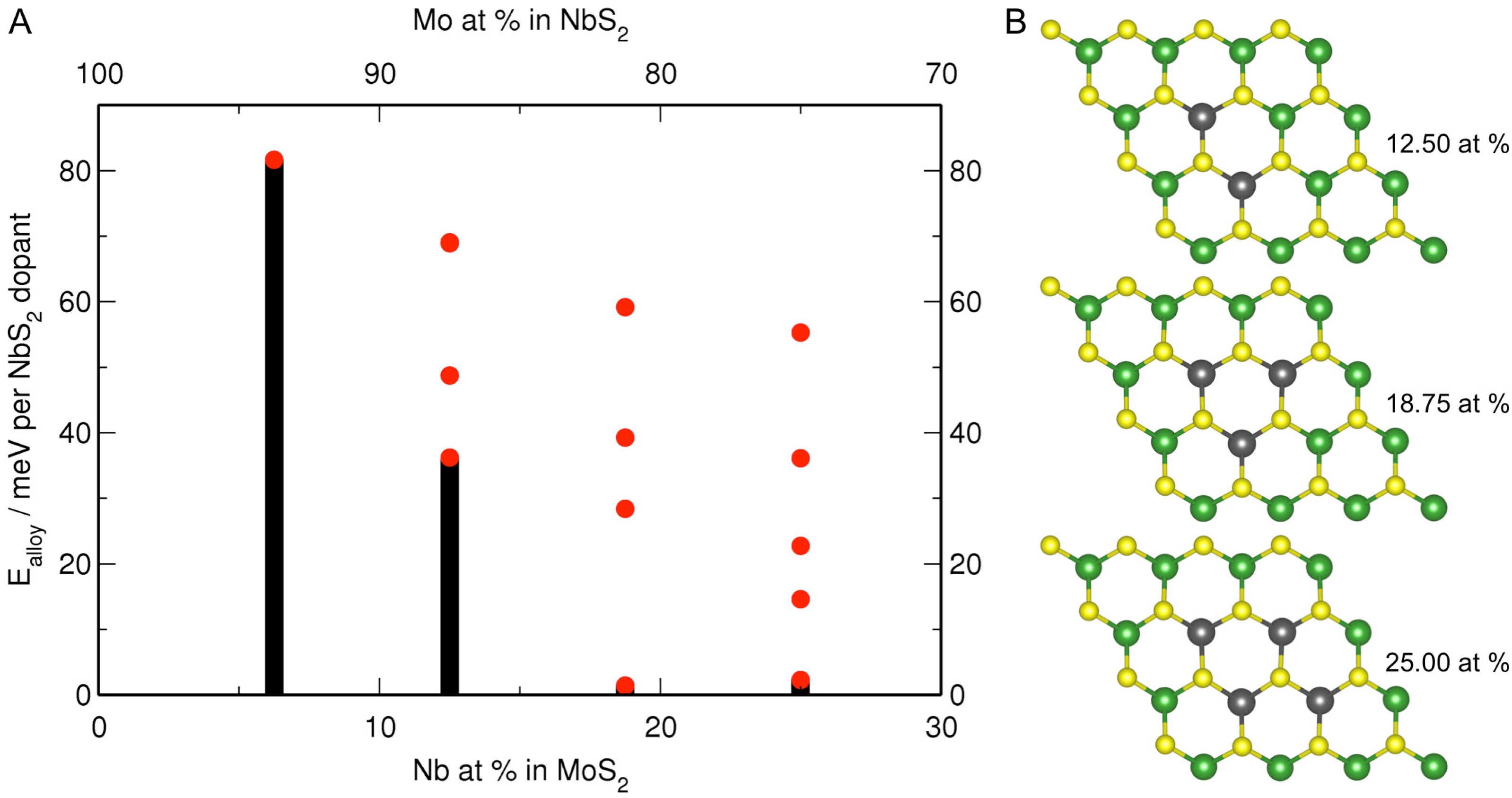
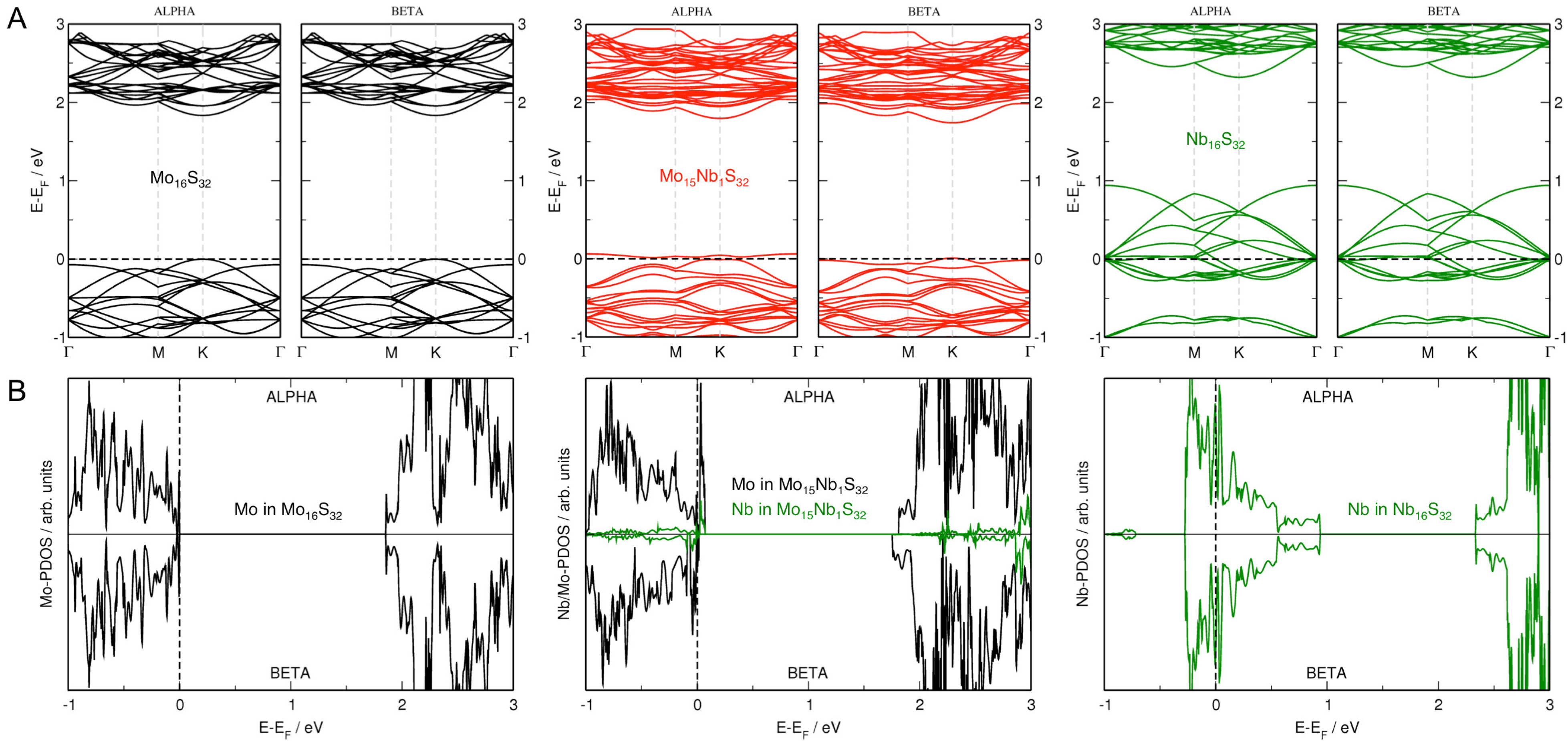
3.2. MoS Alloys with Nb
| Formula | Nb at% | a, b | Nb–Nb |
|---|---|---|---|
| MoS | 0.00 | 12.683 (12.656) | – |
| MoNbS | 6.25 | 12.678 | – |
| MoNbS | 12.50 | 12.675 | 3.325 |
| MoNbS | 18.75 | 12.672 | 3.380 |
| MoNbS | 25.00 | 12.669 | 3.394 |
| NbS | 100.00 | 13.348 (13.240) | 3.338 |


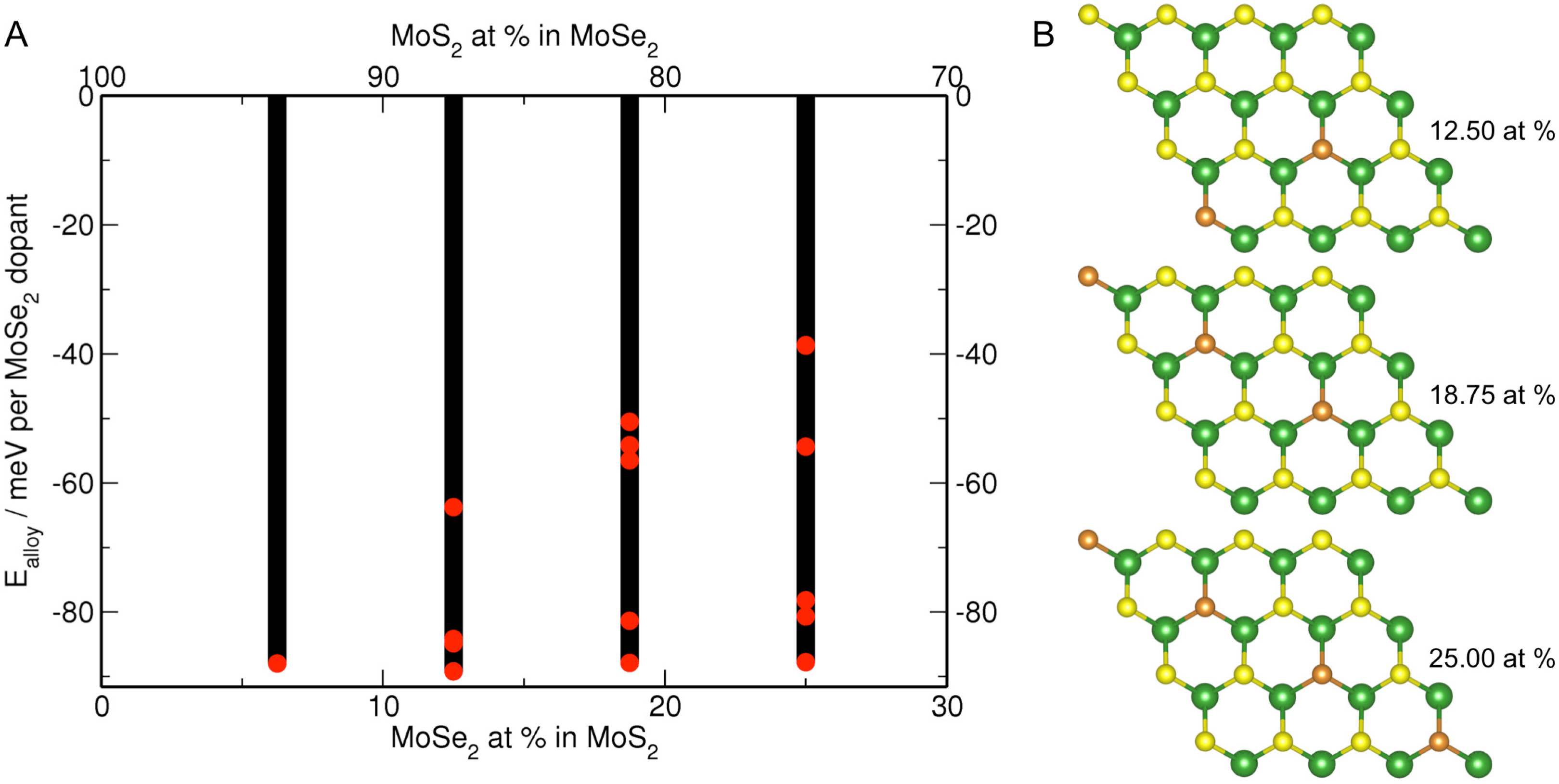
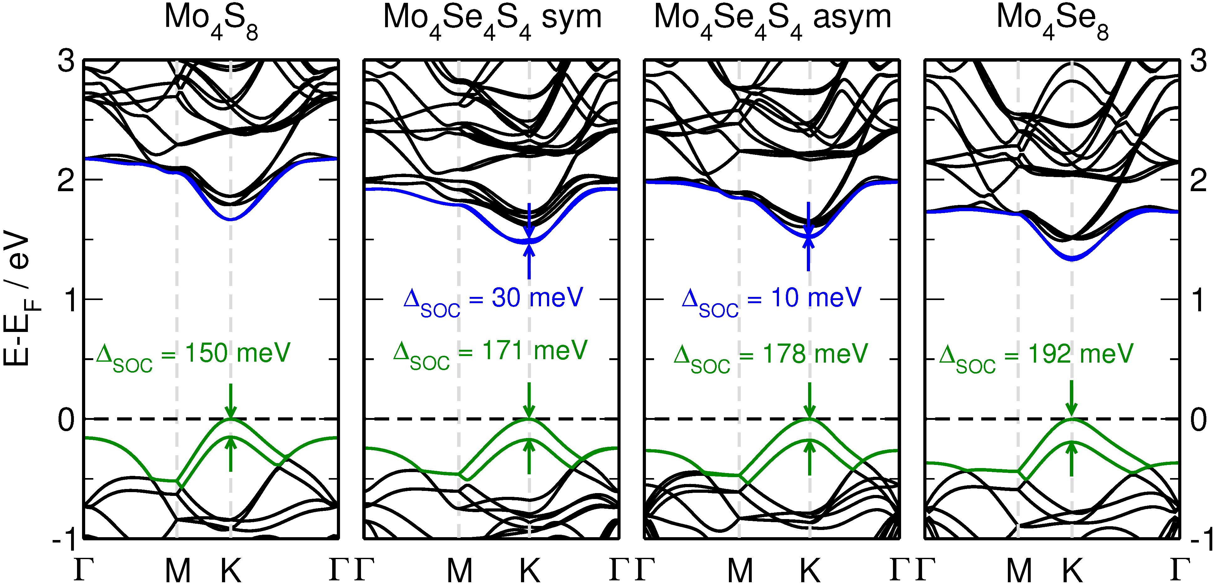
3.3. MoS Alloys with Se
| Formula | MoSe at% | a, b | Se–Se | Δ |
|---|---|---|---|---|
| MoS | 0.00 | 12.683 (12.656) | – | 1.90 (1.80) |
| MoSSe | 6.25 | 12.710 | – | 1.81 |
| MoSSe | 12.50 | 12.738 | 5.520 | 1.79 |
| MoSSe | 18.75 | 12.767 | 5.532 | 1.77 |
| MoSSe | 25.00 | 12.795 | 5.540 | 1.75 |
| MoSSe | 50.00 symmetric | 12.915 | 3.246 | 1.63 |
| MoSSe | 50.00 asymmetric | 12.903 | 3.243 | 1.68 |
| MoSe | 100.00 | 13.261 (13.152) | 3.288 | 1.53 (1.55) |


4. Conclusions
Acknowledgments
Author Contributions
Conflicts of Interest
References
- Mak, K.F.; Lee, C.; Hone, J.; Shan, J.; Heinz, T.F. Atomically Thin MoS2: A New Direct-Gap Semiconductor. Phys. Rev. Lett. 2010, 105, 136805. [Google Scholar] [CrossRef] [PubMed]
- Splendiani, A.; Sun, L.; Zhang, Y.B.; Li, T.S.; Kim, J.; Chim, C.Y.; Galli, G.; Wang, F. Emerging Photoluminescence in Monolayer MoS2. Nano Lett. 2010, 10, 1271–1275. [Google Scholar] [CrossRef] [PubMed]
- Kuc, A.; Zibouche, N.; Heine, T. Influence of quantum confinement on the electronic structure of the transition metal sulfide TS2. Phys. Rev. B 2011, 83, 245213. [Google Scholar] [CrossRef]
- Komsa, H.-P.; Krasheninnikov, A.V. Two-Dimensional Transition Metal Dichalcogenide Alloys: Stability and Electronic Properties. J. Phys. Chem. Lett. 2012, 3, 3652–3656. [Google Scholar] [CrossRef] [PubMed]
- Ataca, C.; Sahin, H.; Ciraci, S. Stable, Single-Layer MX2 Transition-Metal Oxides and Dichalcogenides in a Honeycomb-Like Structure. J. Phys. Chem. C 2012, 116, 8983–8999. [Google Scholar] [CrossRef] [Green Version]
- Zibouche, N.; Philipsen, P.; Kuc, A.; Heine, T. Transition-metal dichalcogenide bilayers: Switching materials for spintronic and valleytronic applications. Phys. Rev. B 2014, 90, 125440. [Google Scholar] [CrossRef]
- Ramasubramaniam, A.; Naveh, D.; Towe, E. Tunable band gaps in bilayer transition-metal dichalcogenides. Phys. Rev. B 2011, 84, 205325. [Google Scholar] [CrossRef]
- Ghorbani-Asl, M.; Zibouche, N.; Wahiduzzaman, M.; Oliveira, A.F.; Kuc, A.; Heine, T. Electromechanics in MoS2 and WS2: Nanotubes vs. monolayers. Sci. Rep. 2013, 3, 2961. [Google Scholar] [CrossRef] [PubMed]
- Johari, P.; Shenoy, V.B. Tuning the Electronic Properties of Semiconducting Transition Metal Dichalcogenides by Applying Mechanical Strains. ACS Nano 2012, 6, 5449–5456. [Google Scholar] [CrossRef] [PubMed]
- Yue, Q.; Kang, J.; Shao, Z.; Zhang, X.; Chang, S.; Wang, G.; Qin, S.; Li, J. Mechanical and electronic properties of monolayer MoS2 under elastic strain. Phys. Lett. A 2012, 376, 1166–1170. [Google Scholar] [CrossRef]
- Yun, W.S.; Han, S.W.; Hong, S.C.; Kim, I.G.; Lee, J.D. Thickness and strain effects on electronic structures of transition metal dichalcogenides: 2H-MX2 semiconductors (M = Mo, W; X = S, Se, Te). Phys. Rev. B 2012, 85, 033305. [Google Scholar] [CrossRef]
- Zhu, Z.Y.; Cheng, Y.C.; Schwingenschlögl, U. Giant spin-orbit-induced spin splitting in two-dimensional transition-metal dichalcogenide semiconductors. Phys. Rev. B 2011, 84, 153402. [Google Scholar] [CrossRef]
- Zibouche, N.; Kuc, A.; Musfeldt, J.; Heine, T. Transition-metal dichalcogenides for spintronic applications. Ann. der Phys. 2014, 526, 395–401. [Google Scholar] [CrossRef]
- Nayak, A.P.; Bhattacharyya, S.; Zhu, J.; Liu, J.; Wu, X.; Pandey, T.; Jin, C.; Singh, A.K.; Akinwande, D.; Lin, J.-F. Pressure-induced semiconducting to metallic transition in multilayered molybdenum disulphide. Nat. Commun. 2014, 5, 3731. [Google Scholar] [CrossRef] [PubMed]
- Zhao, Z.; Zhang, H.; Yuan, H.; Wang, S.; Lin, Y.; Zeng, Q.; Xu, G.; Liu, Z.; Solanki, G.K.; Patel, K.D.; et al. Pressure induced metallization with absence of structural transition in layered molybdenum diselenide. Nat. Commun. 2015, 6, 7312. [Google Scholar] [CrossRef] [PubMed]
- Yadgarov, L.; Rosentsveig, R.; Leitus, G.; Albu-Yaron, A.; Moshkovich, A.; Perfilyev, V.; Vasic, R.; Frenkel, A.I.; Enyashin, A.N.; Seifert, G.; et al. Controlled Doping of MS2 (M=W, Mo) Nanotubes and Fullerene-like Nanoparticles. Angew. Chem. Int. Edit. 2012, 51, 1148–1151. [Google Scholar] [CrossRef] [PubMed]
- Ivanovskaya, V.V.; Heine, T.; Gemming, S.; Seifert, G. Structure, stability and electronic properties of composite Mo1xNbxS2 nanotubes. Phys. Stat. Solidi B 2006, 243, 1757–1764. [Google Scholar] [CrossRef]
- Ivanovskaya, V.V.; Seifert, G.; Ivanovskii, A.L. Electronic structure of niobium-doped molybdenum disulfide nanotubes. Russ. J. Inorg. Chem. 2006, 51, 320–324. [Google Scholar] [CrossRef]
- Ivanovskaya, V.V.; Zobelli, A.; Gloter, A.; Brun, N.; Serin, V.; Colliex, C. Ab initio study of bilateral doping within the MoS2-NbS2 system. Phys. Rev. B 2008, 78, 134104. [Google Scholar] [CrossRef]
- Tan, C.-K.; Tansu, N. Auger recombination rates in dilute-As GaNAs semiconductor. AIP Adv. 2015, 5, 057135. [Google Scholar] [CrossRef]
- Kimura, A.; Paulson, C.A.; Tang, H.F.; Kuech, T.F. Epitaxial GaN1yAsy layers with high As content grown by metalorganic vapor phase epitaxy and their band gap energy. Appl. Phys. Let. 2004, 84, 1489–1491. [Google Scholar] [CrossRef]
- Tansu, N.; Yeh, J.-Y.; Mawst, L. High-Performance 1200-nm InGaAs and 1300-nm InGaAsN Quantum Well Lasers by Metalorganic Chemical Vapor Deposition. Sel. Top. Quantum Electron. IEEE 2003, 9, 1220–1227. [Google Scholar] [CrossRef]
- Bank, S.; Goddard, L.; Wistey, M.A.; Yuen, H.B.; Harris, J.S. On the temperature sensitivity of 1.5-µm GaInNAsSb lasers. Sel. Top. Quantum Electron. IEEE 2005, 11, 1089–1098. [Google Scholar] [CrossRef]
- Gan, L.-Y.; Zhang, Q.; Zhao, Y.-J.; Cheng, Y.; Schwingenschlögl, U. Order-disorder phase transitions in the two-dimensional semiconducting transition metal dichalcogenide alloys Mo1xWxX2 (X = S, Se, and Te). Sci. Rep. 2014, 4, 6691. [Google Scholar] [CrossRef] [PubMed]
- Kutana, A.; Penev, E.S.; Yakobson, B.I. Engineering electronic properties of layered transition-metal dichalcogenide compounds through alloying. Nanoscale 2014, 6, 5820–5825. [Google Scholar] [CrossRef] [PubMed]
- Wang, G.; Robert, C.; Suslu, A.; Chen, B.; Yang, S.; Alamdari, S.; Gerber, I.C.; Amand, T.; Marie, X.; Tongay, S.; et al. Spin-orbit engineering in transition metal dichalcogenide alloy monolayers. Nat. Commun. 2015. [Google Scholar] [CrossRef] [PubMed]
- Liu, H.; Antwi, K.K.A.; Chua, S.; Chi, D. Vapor-phase growth and characterization of Mo1xWxS2 (0 ≤ x ≤ 1) atomic layers on 2-inch sapphire substrates. Nanoscale 2014, 6, 624–629. [Google Scholar] [CrossRef] [PubMed]
- Chen, Y.; Dumcenco, D.O.; Zhu, Y.; Zhang, X.; Mao, N.; Feng, Q.; Zhang, M.; Zhang, J.; Tan, P.-H.; Huang, Y.-S.; et al. Composition-dependent Raman modes of Mo1xWxS2 monolayer alloys. Nanoscale 2014, 6, 2833–2839. [Google Scholar] [CrossRef] [PubMed]
- Ren, X.; Ma, Q.; Fan, H.; Pang, L.; Zhang, Y.; Yao, Y.; Ren, X.; Liu, S.F. A Se-doped MoS2 nanosheet for improved hydrogen evolution reaction. Chem. Commun. 2015, 51, 15997–16000. [Google Scholar] [CrossRef] [PubMed]
- Faraji, M.; Sabzali, M.; Yousefzadeh, S.; Sarikhani, N.; Ziashahabi, A.; Zirak, M.; Moshfegh, A.Z. Band engineering and charge separation in the Mo1xWxS2/TiO2 heterostructure by alloying: First principle prediction. RSC Adv. 2015, 5, 28460–28466. [Google Scholar] [CrossRef]
- Dovesi, R.; Saunders, V.R.; Roetti, R.; Orlando, R.; Zicovich-Wilson, C.M.; Pascale, F.; Civalleri, B.; Doll, K.; Harrison, N.M.; Bush, I.J.; et al. CRYSTAL09 User’s Manual; University of Torino: Torino, Canada, 2009. [Google Scholar]
- Perdew, J.P.; Burke, K.; Ernzerhof, M. Generalized Gradient Approximation Made Simple. Phys. Rev. Lett. 1996, 77, 3865. [Google Scholar] [CrossRef] [PubMed]
- Cora, F.; Patel, A.; Harrison, N.M.; Roetti, C.; Catlow, C.R.A. An ab-initio Hartree-Fock study of alpha-MoO3. J. Mater. Chem. 1997, 7, 959. [Google Scholar] [CrossRef]
- Cora, F.; Patel, A.; Harrison, N.M.; Dovesi, R.; Catlow, C.R.A. An ab-initio Hartree-Fock study of the cubic and tetragonal phases of Bulk Tungsten Trioxide. J. Am. Chem. Soc. 1996, 118, 12174. [Google Scholar] [CrossRef]
- Dall’Olio, S.; Dovesi, R.; Resta, R. Spontaneous polarization as a Berry phase of the Hartree-Fock wave function: The case of KNbO3. Phys. Rev. B 1997, 56, 10105–10114. [Google Scholar] [CrossRef]
- Te Velde, G.; Baerends, E. J. Precise density-functional method for periodic structures. Phys. Rev. B 1991, 44, 7888–7903. [Google Scholar] [CrossRef]
- Philipsen, P.; te Velde, G.; Bearends, E.; Berger, J.; de Boeij, P.; Groenveld, J.; Kadantsev, E.; Klooster, R.; Kootstra, F.; Romaniello, P.; et al. BAND2012, SCM, Theoretical Chemistry; Vrije Universiteit: Amsterdam, Netherlands, 2012. [Google Scholar]
- Monkhorst, H.J.; Pack, J.D. Special points for Brillouin-zone integrations. Phys. Rev. B 1976, 13, 5188. [Google Scholar] [CrossRef]
- Wilson, J.A.; Yoffe, A.D. The transition metal dichalcogenides discussion and interpretation of the observed optical, electrical and structural properties. Adv. Phys. 1969, 18, 193–335. [Google Scholar] [CrossRef]
- Mattheis, L.F. Band Structures of Transition-Metal-Dichalcogenide Layer Compounds. Phys. Rev. B 1973, 8, 3719. [Google Scholar] [CrossRef]
- Coehoorn, R.; Haas, C.; Dijkstra, J.; Flipse, C.J.F.; Degroot, R.A.; Wold, A. Electronic structure of MoSe2, MoS2, and WSe2. I. Band-structure calculations and photoelectron spectroscopy. Phys. Rev. B 1987, 35, 6195–6202. [Google Scholar] [CrossRef]
- Tongay, S.; Zhou, J.; Ataca, C.; Lo, K.; Matthews, T.S.; Li, J.; Grossman, J.C.; Wu, J. Thermally Driven Crossover from Indirect toward Direct Bandgap in 2D Semiconductors: MoSe2 versus MoS2. Nano Lett. 2012, 12, 5576–5580. [Google Scholar] [CrossRef] [PubMed]
- Kang, J.; Tongay, S.; Li, J.; Wu, J. Monolayer semiconducting transition metal dichalcogenide alloys: Stability and band bowing. J. Appl. Phys. 2013, 113, 143703. [Google Scholar] [CrossRef]
© 2015 by the authors; licensee MDPI, Basel, Switzerland. This article is an open access article distributed under the terms and conditions of the Creative Commons by Attribution (CC-BY) license (http://creativecommons.org/licenses/by/4.0/).
Share and Cite
Kuc, A.; Heine, T. On the Stability and Electronic Structure of Transition-Metal Dichalcogenide Monolayer Alloys Mo1−xXxS2−ySey with X = W, Nb. Electronics 2016, 5, 1. https://doi.org/10.3390/electronics5010001
Kuc A, Heine T. On the Stability and Electronic Structure of Transition-Metal Dichalcogenide Monolayer Alloys Mo1−xXxS2−ySey with X = W, Nb. Electronics. 2016; 5(1):1. https://doi.org/10.3390/electronics5010001
Chicago/Turabian StyleKuc, Agnieszka, and Thomas Heine. 2016. "On the Stability and Electronic Structure of Transition-Metal Dichalcogenide Monolayer Alloys Mo1−xXxS2−ySey with X = W, Nb" Electronics 5, no. 1: 1. https://doi.org/10.3390/electronics5010001