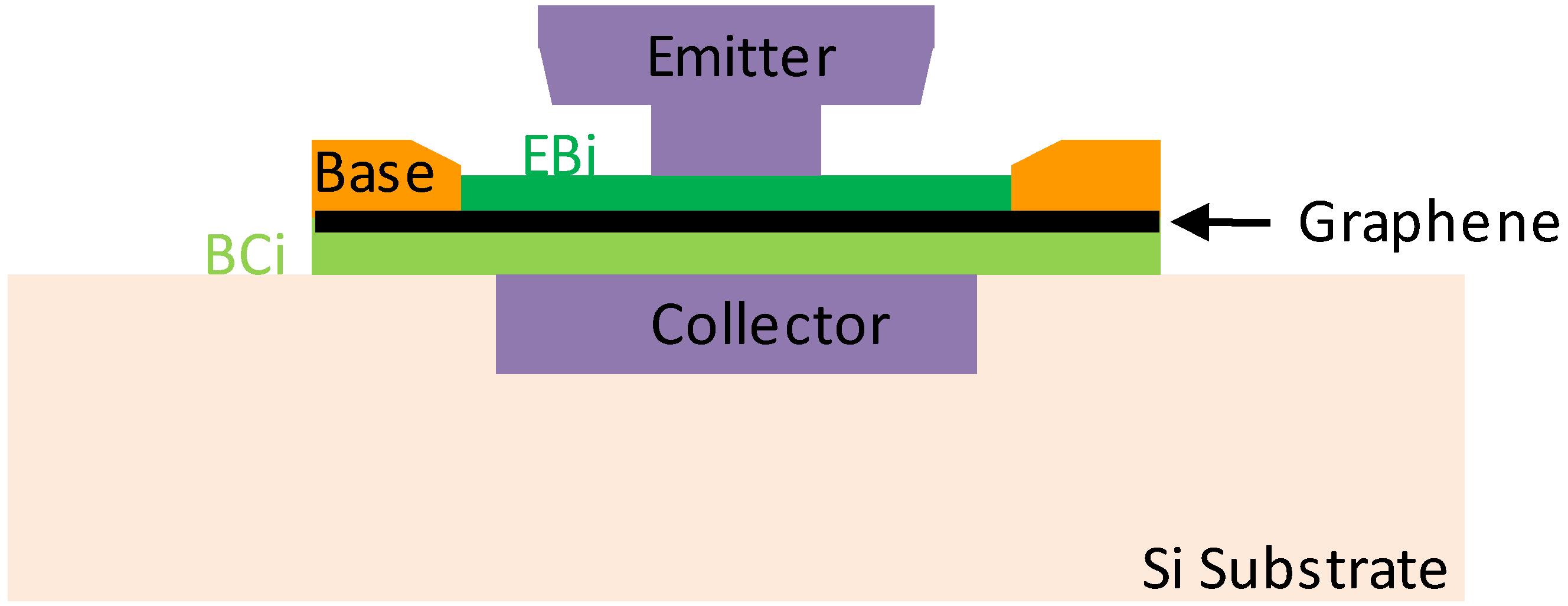
The GBT transistor structure is presented in
Figure 1. The vertical stack comprises the emitter, the emitter-base region EBi, the graphene base, the base-collector region BCi and the collector. The barrier potential height of the EBi and BCi regions controls the carrier transport mode such as tunneling or thermionic transport. Hence, the choice of the material used for the EBi and BCi region is of major importance. EBi and BCi can be either an insulator material such as SiO
2 or high-k dielectrics to exploit a tunneling transport [
6] or a semiconductor such as Ge or Si to foster a thermionic current [
12].
Figure 1.
Schematic representation of the transistor structure.
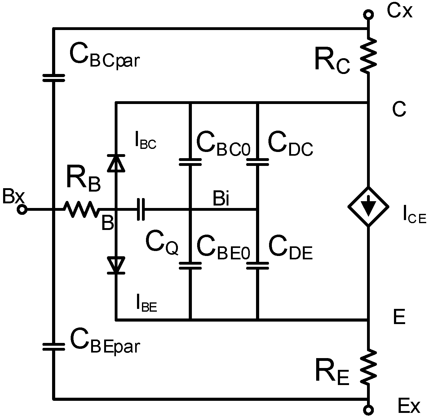
According to the transistor structure (see
Figure 1), the following equivalent circuit is proposed (see
Figure 2). The extrinsic circuit is composed of three access resistances
RB,
RC,
RE. Concerning the intrinsic part, the core of the model is based on the self-consistent calculation of the internal base potential
VBi, which is a function of the charge in the emitter, the collector and within the graphene layer. These charges are modeled through different capacitances. First,
CQ capacitance models the quantum capacitance of the graphene layer, while
CBE0 and
CBC0 describe the EBi and BCi capacitances, respectively. Finally,
CDC and
CDE are diffusion capacitances that take into account the additional charge due to carrier transport in the EBi and BCi regions. These capacitances are of interest for medium to high injection conditions [
9]. Finally, two diodes I
BE and I
BC are modeling the base-emitter and base-collector current, respectively, and one voltage controlled current source
ICE is introduced for the collector-emitter transfer current. Each element is described in the next section.
Figure 2.
Equivalent circuit of the Graphene Base Transistor (GBT) electrical compact model.
2.1. Self-Consistent Calculation of the Internal Base Potential
The charge in the graphene layer can be computed by combining the specific density of states of graphene with the Fermi approach for the carrier distribution. Assuming that the potential drop into the graphene base |
VBBi| ≫ k
T/
q (k is the Boltzmann constant,
T is the absolute temperature and
q is the elementary charge), the total charge density can be approximated as follows [
13]:
with
ћ the reduced Planck constant,
vf the Fermi velocity and
,
.
Introducing the graphene charge in the equivalent circuit, the internal base potential can be calculated by solving the following equation:
where
VBiC =
VBi −
VC,
VBiE =
VBi −
VE,
CBC =
CBC0 +
CDC,
CBE =
CBE0 +
CDE (see
Figure 2) and
,
are the oxide capacitances.
eBC and
eBE are the insulator thicknesses of
EBi and
BCi regions, respectively, and ε
BE and ε
BC are the associated permittivity.
AE is the emitter area. The diffusion capacitances
CDE and
CDC will be described in Section II-C.
Substituting Equation (1) in Equation (2), the
VBBi potential is introduced in the equation:
Equation (3) is a second order polynomial that can be solved and gives the following solution [
6]:
2.1.1. Description of Diodes and Transfer Current Source
As described above, the EBi and BCi material can be either insulator or semiconductor and the charge transport can be dominated by tunneling emission or thermionic transport. In order to obtain a versatile compact model, the diode and transfer current source equations will be based on flexible and simple relationships.
For the base-emitter and base-collector tunnel or semiconductor-graphene diodes, an exponential equation is used (see [
14]) and modified to gain in adaptability:
where
JSBE and
JSBC are the corresponding saturation currents, ϕ
BE and ϕ
BC are the barrier heights and
BBE and
BBC are fitting parameters of the slope of the exponential function.
For the transfer current source, a modified Landauer based equation is used [
15].
JSF is a saturation current and the fCE parameter allows zeroing the current if the collector-emitter barrier ϕCE is too high to be crossed by the carrier at low VCE. ϕCE is used as a fitting parameter for the low VCE bias regime.
2.1.2. Medium to High Current Injection Effects
At medium to high current conditions, the charge injected through the transfer current in the EBi and BCi junctions needs to be taken into account. This charge will modify the charge equilibrium in the intrinsic transistor and will induce a shift of the internal base potential. Hence, as suggested in
Figure 2, diffusion capacitances are included in the equivalent circuit and this will affect the potential drop
VBBi through the Equation (4).
The diffusion charge within the two regions is computed by considering a transit time approach. At medium injection level, the charge can be approximated by
,
are the transit times of the BCi and EBi region at medium injection, respectively. At high injection, an additional charge
[
9,
12], with respect to
QDE appears when the transfer current
ICE overpass the critical current
ICK:
is the additive transit time at high injection and γ is a fitting parameter.
Combining Equations (8) and (9) and deriving the equation, the related capacitance can be deduced:
These elements can be either derived analytically or directly computed using a derivative function in Verilog language.
2.2. Comparison to Numerical Simulation
In order to validate our model and to demonstrate its physical basis, a comparison between physics-based numerical simulations and our compact model is provided. The 1-D numerical model of [
9] solves the electrostatics of the GBT self-consistently with the calculated tunneling current and estimates the transit frequency
fT. Concerning the currents, since the physical origin of the base current is still unclear and debated [
7,
16], a perfectly transparent graphene layer is assumed and the base current is neglected. Hence, we assume a priori that the collector current is the current due to electrons injected from the emitter and, consistently, crossing the whole device.
The simulated device assumes that the EBi and BCi layers are made of two insulators [
11]: the EBi region has a 2 nm high permittivity insulator (ε
r = 25) while the BCi region has a 12 nm oxide with ε
r = 2.5. Only the intrinsic device is simulated and one would need to consider parasitic elements to have a realistic circuit simulation.
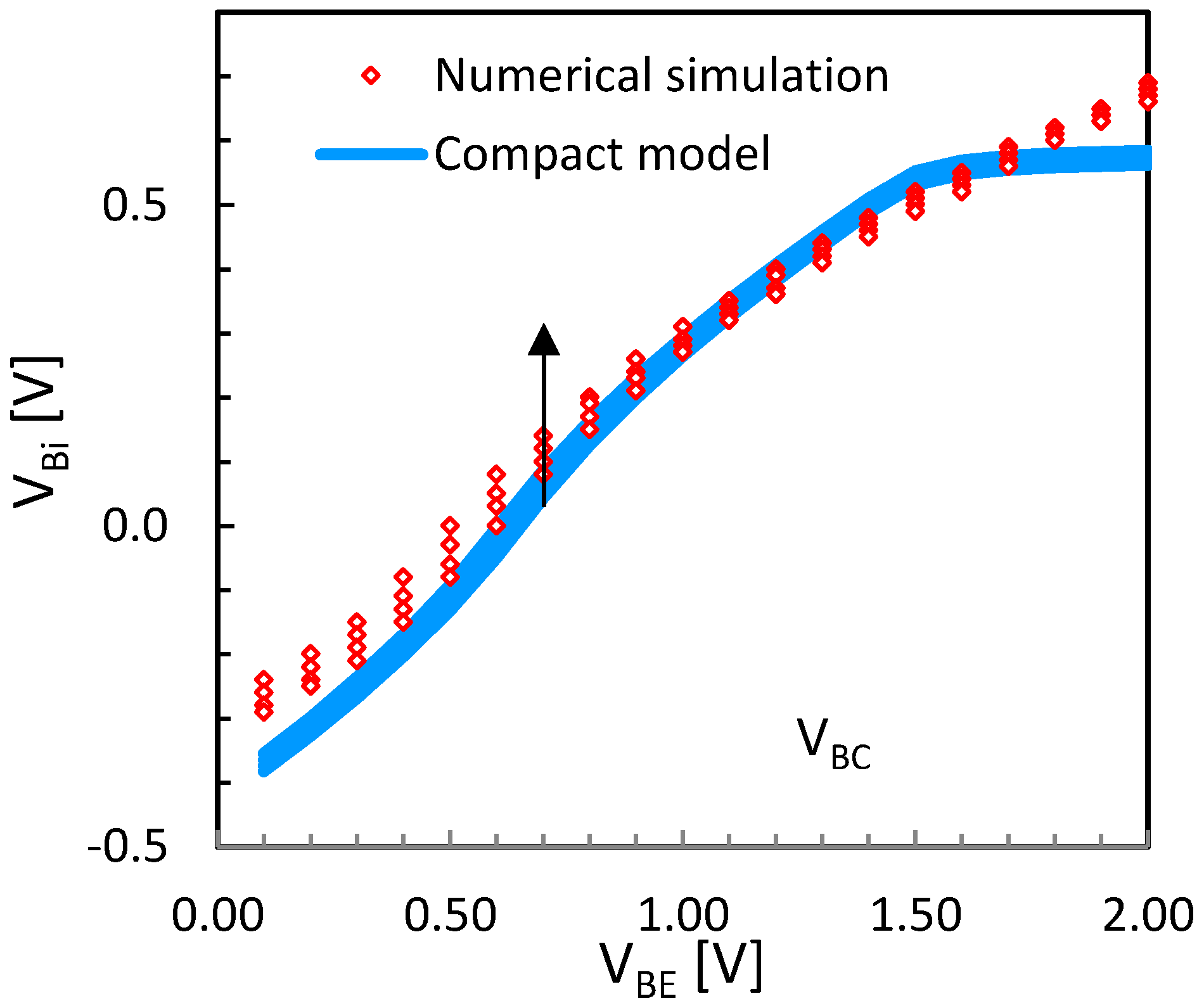
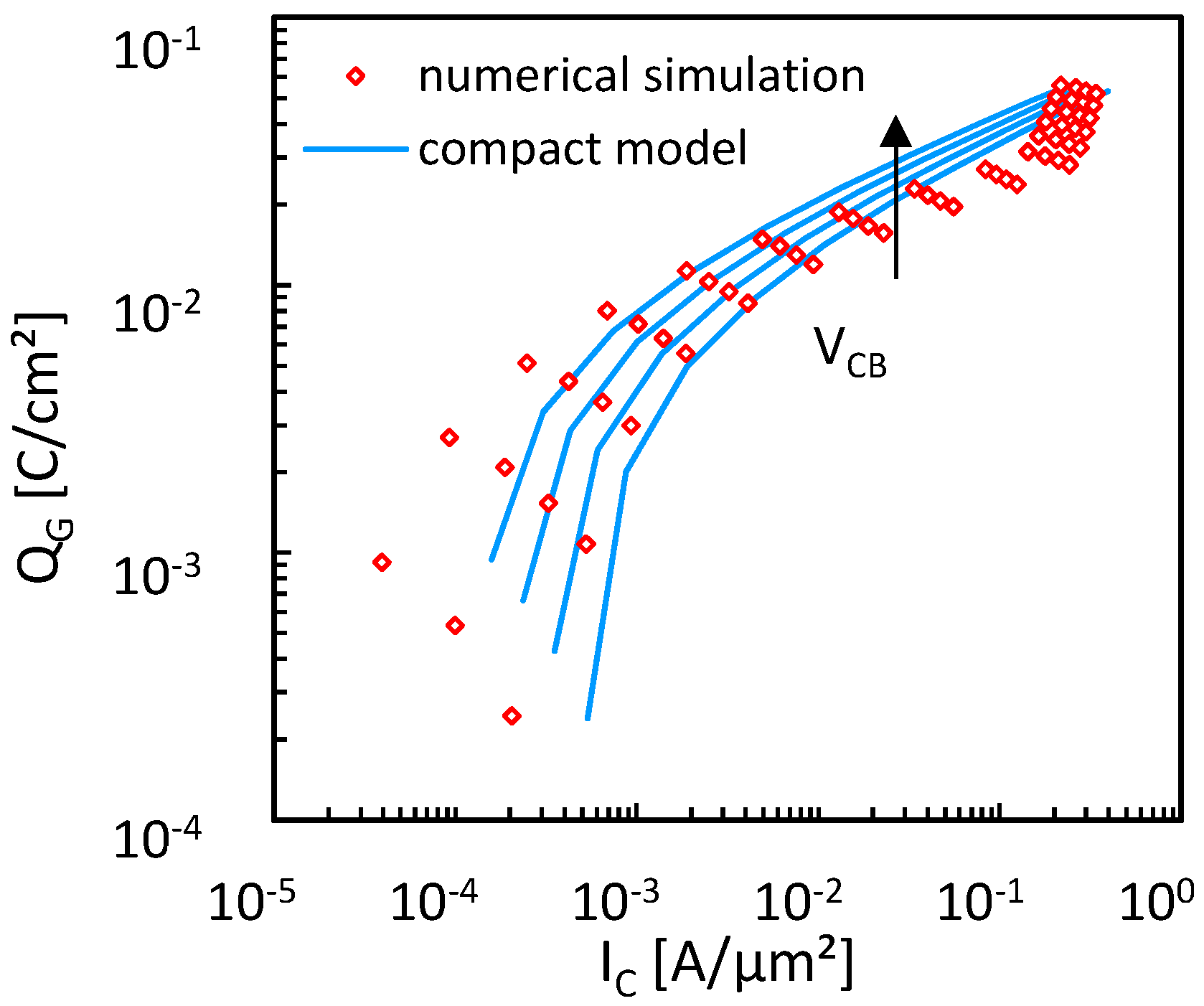
First, a comparison between numerical simulations and compact model simulations of the calculated graphene base charge is provided in
Figure 3. Despite a deviation at large
ICE mainly due to different modeling approaches for the high injection effects (model in [
9] solves the potential along the device self-consistently with the traveling electrons), a fairly good agreement is found between the two models. This verifies the adequate calculation of the intrinsic base potential
VBi by the compact model (see
Figure 4).
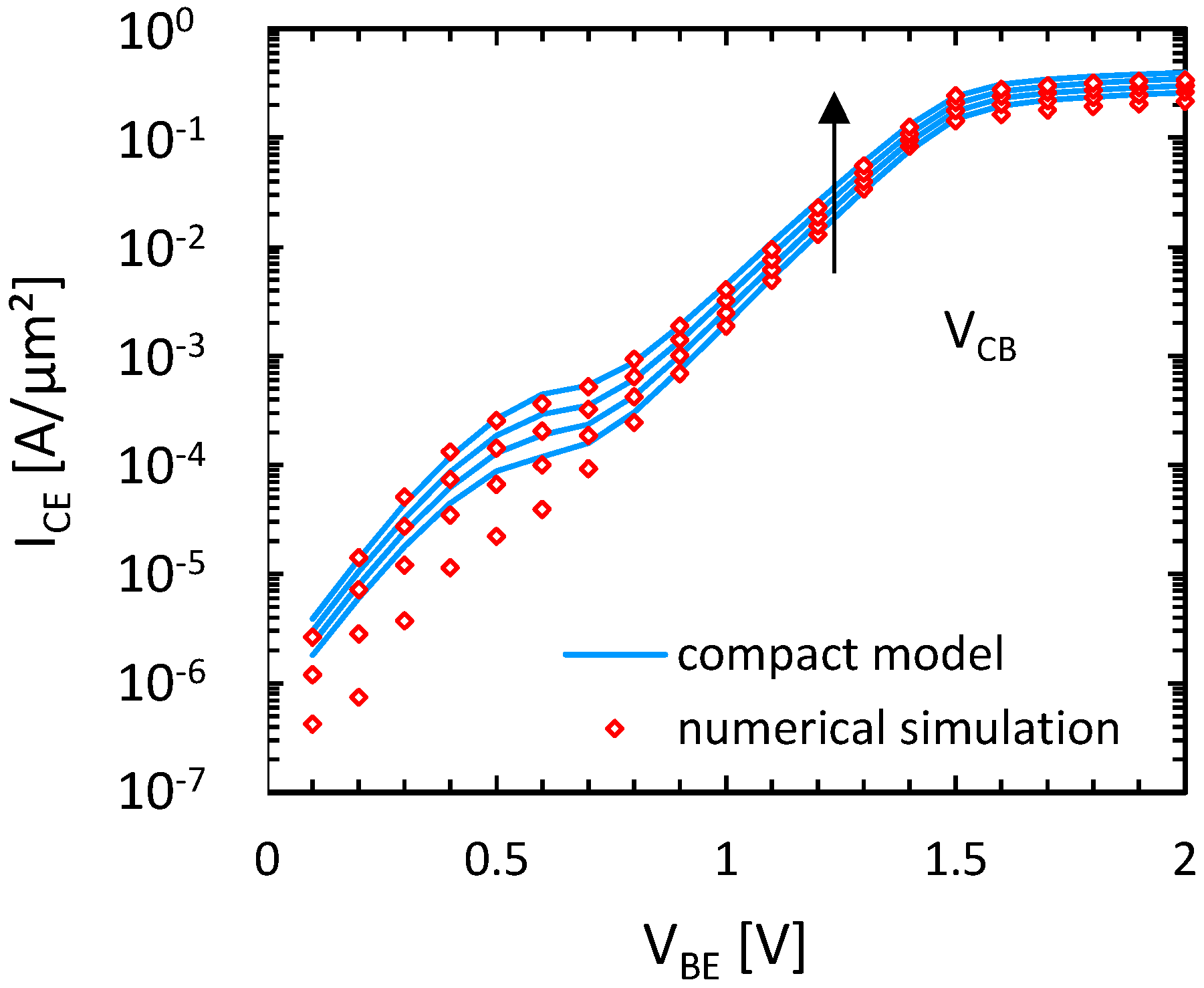
The transfer characteristics of the device are simulated in
Figure 5. At low injection condition, a similar behavior is observed despite a small disagreement. A good agreement is observed at medium to high electron injection levels.
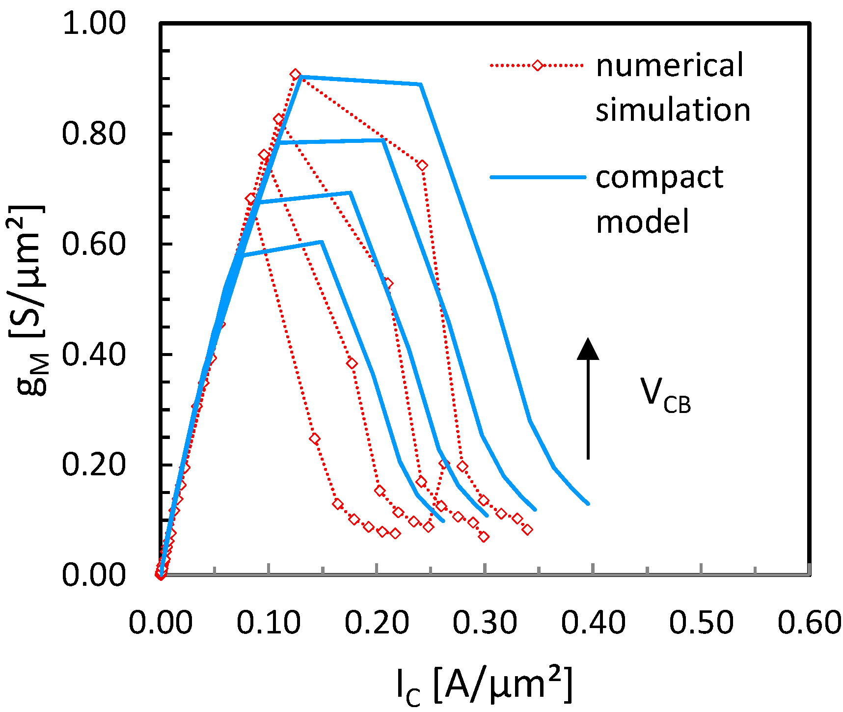
Figure 6, instead, shows the associated transconductance, which is of major importance for RF circuit simulation. A very good agreement is observed for low and medium bias, a reasonable agreement can be found for high bias. Finally,
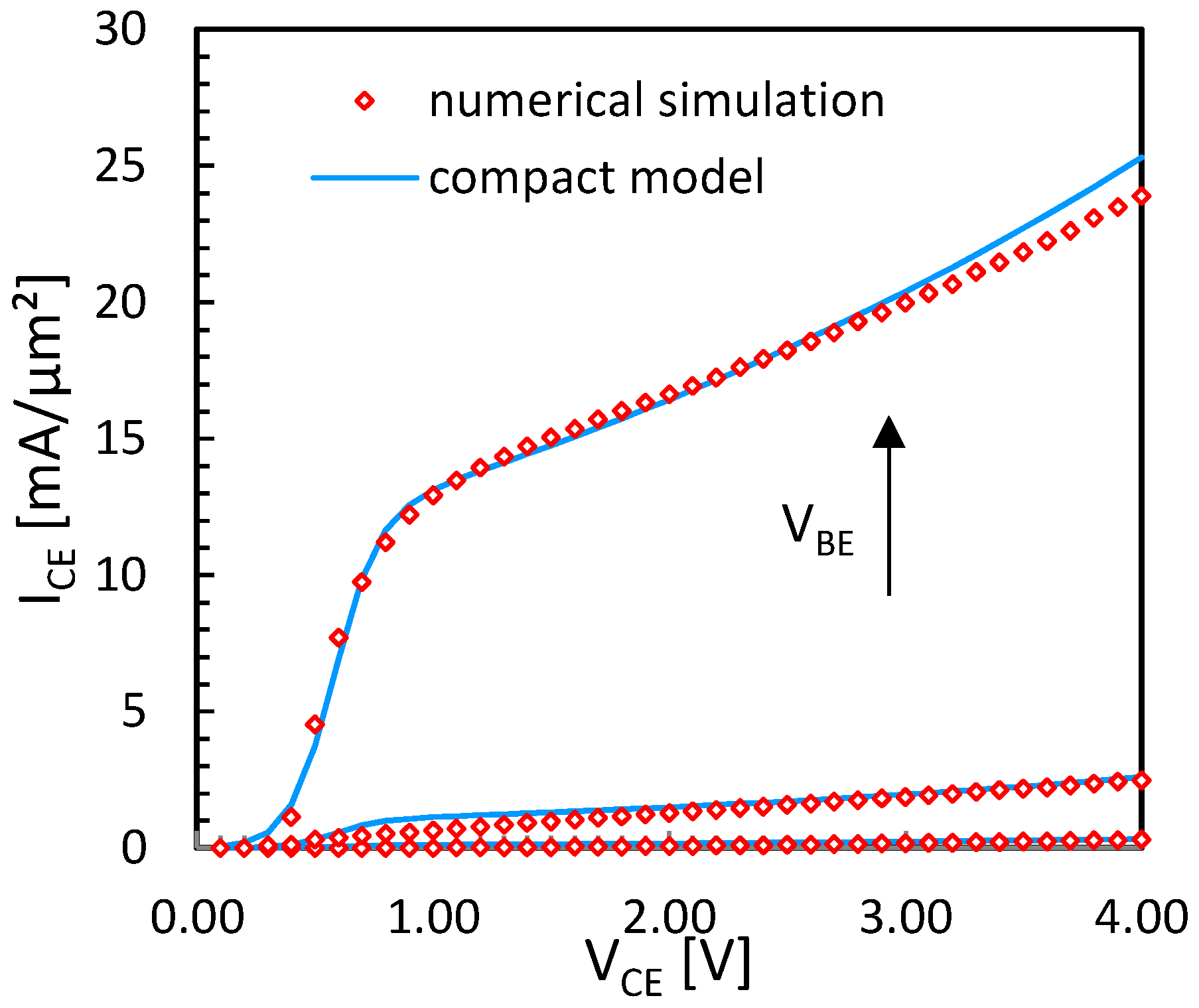
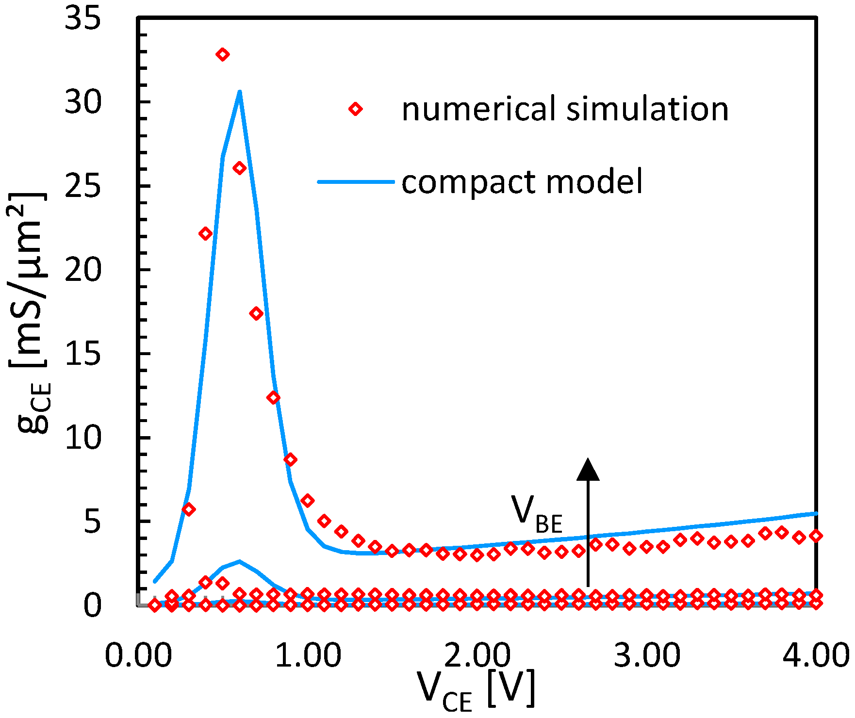
Figure 7 compares the output curves confirming a good matching between the two models. It should be underlined that the slope
gCE (see
Figure 8) is properly modeled; this is mandatory to correctly model the voltage gain of an amplifier circuit.
Figure 3.
Charge QG versus ICE curves for different VCB (2, 3, 4, 5 V), numerical simulation and compact model simulation.
Figure 3.
Charge QG versus ICE curves for different VCB (2, 3, 4, 5 V), numerical simulation and compact model simulation.
Figure 4.
Graphene Fermi potential versus VBE curves for different VCB (2, 3, 4, 5 V), numerical simulation and compact model simulation.
Figure 4.
Graphene Fermi potential versus VBE curves for different VCB (2, 3, 4, 5 V), numerical simulation and compact model simulation.
Figure 5.
ICE versus VBE curves for different VCB values (2, 3, 4, 5 V) simulated with the numerical model and the compact model.
Figure 5.
ICE versus VBE curves for different VCB values (2, 3, 4, 5 V) simulated with the numerical model and the compact model.
Figure 6.
gM versus IC curves for different VCB (2, 3, 4, 5 V) simulated with the numerical model and the compact model.
Figure 6.
gM versus IC curves for different VCB (2, 3, 4, 5 V) simulated with the numerical model and the compact model.
Figure 7.
ICE versus VCE curves for different VBE values (0.75, 1, 1.25 V), numerical simulation and compact model simulation.
Figure 7.
ICE versus VCE curves for different VBE values (0.75, 1, 1.25 V), numerical simulation and compact model simulation.
Figure 8.
gCE versus VCE curves for different VBE values (0.75, 1, 1.25 V), numerical simulation and compact model simulation.
Figure 8.
gCE versus VCE curves for different VBE values (0.75, 1, 1.25 V), numerical simulation and compact model simulation.
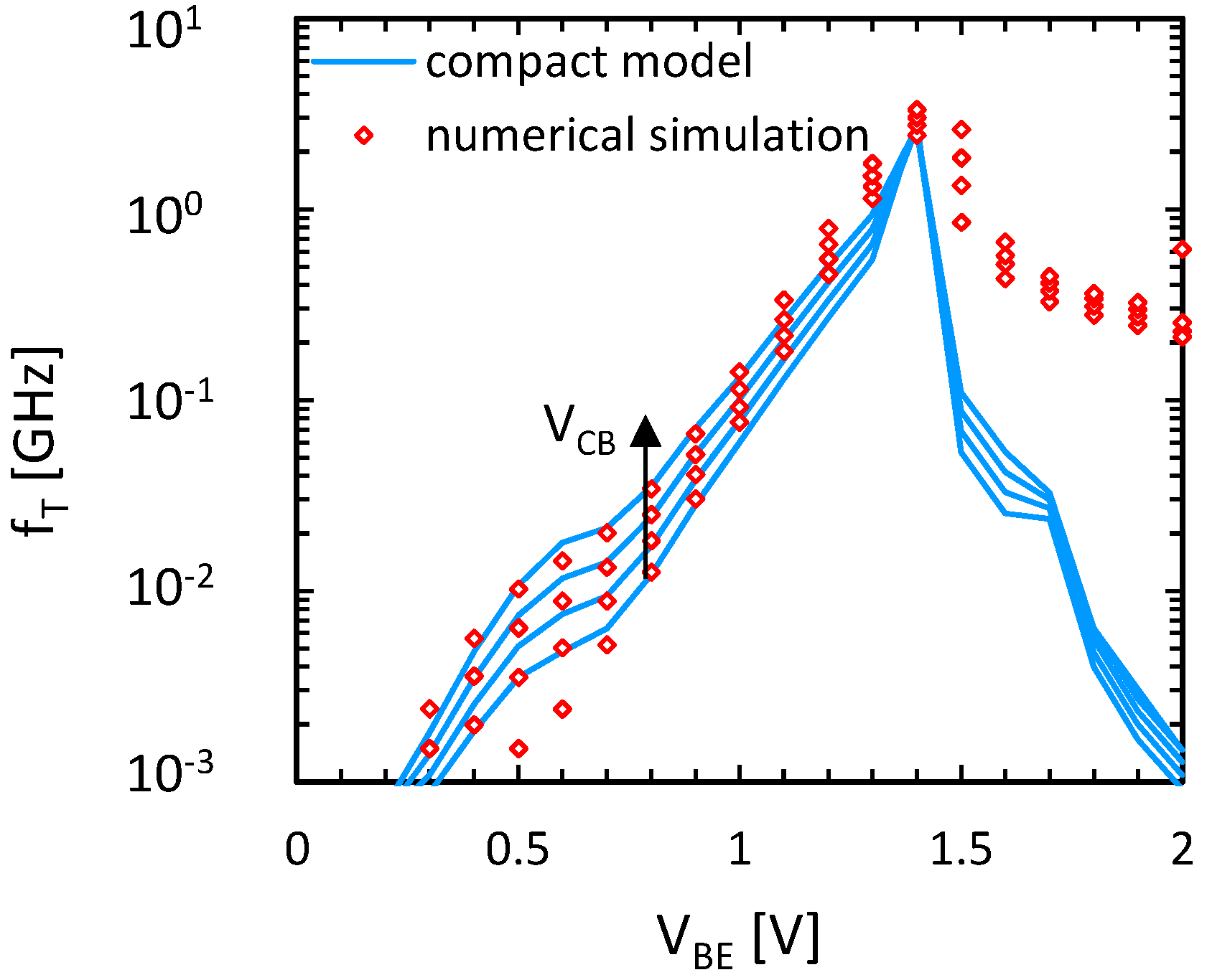
In addition,
S parameter simulations have been performed to extract the transit frequency;
fT is then compared to numerical simulation results (see
Figure 9). A good agreement is observed up to peak
fT, which is the optimum bias condition for circuit applications. At higher current levels, a deviation is observed. Again this can be due to the different modeling strategies adopted to model the high current effects in the GBT.
Table 1.
Parameters used in the compact model simulation.
Table 1.
Parameters used in the compact model simulation.
| Parameter Name/Unit | Parameter Value |
|---|
| JSF (mA/µm2) | 437 |
| BBE (mV) | 35.3 |
| BBC (mV) | 94.2 |
| ΦCE (V) | 0.57 |
| eBE (nm) | 2 |
| eBC (nm) | 12 |
| εBE | 25 |
| εBC | 2.5 |
| τBE (fs) | 0.35 |
| τBC (fs) | 6 |
| ΦBE (V) | 0.893 |
| ΦBC (V) | 1.2 |
| γ | 1.55 |
| κ (µF/cm²) | 25 |
| ICK (A/µm²) | 0.7 |
| ΔτK (fs) | 8 × 10⁻³ |
Figure 9.
fT versus VBE curves for different VCB (2, 3, 4, 5 V), numerical simulation and compact model simulation.
Figure 9.
fT versus VBE curves for different VCB (2, 3, 4, 5 V), numerical simulation and compact model simulation.


