2. Experimental Section
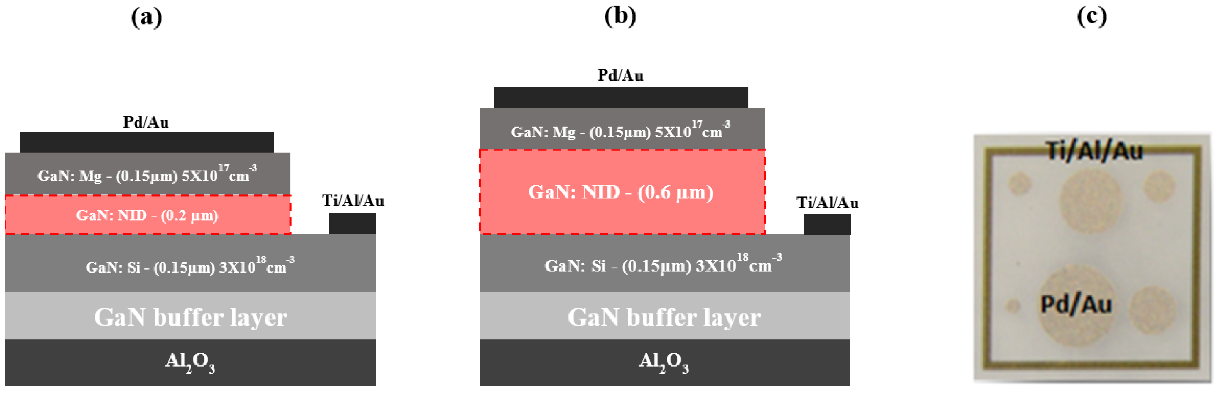
In this study, we have used two GaN p-i-n structures with different thicknesses of the (i-GaN) undoped layer. The use of these structures aims at, on one hand, investigating the impact of the thickness of the (i-GaN) undoped layer on the number of generated electron-hole pairs (EHPs), therefore on the efficiency of betavoltaic conversion, and on the other hand, allowing DLTS study of the depletion region in both i-side and p-side of the p-i-n junction. These structures were grown on 2-inch c-plane sapphire (Al
2O
3) substrates by using a metal-organic vapor phase epitaxy (MOVPE) system (Aixtron, Herzogenrath, Germany). They consist of a 2 µm GaN nucleation layer, which was initially grown as the buffer layer to stop the propagation of defects arising from lattice mismatch between sapphire and GaN epitaxial layers. Then, a 0.2 µm and 0.6 µm–thick undoped GaN layer was grown respectively for sample S1 and S2 acting as the intrinsic region of the diode. This layer is surrounded by a 0.15 µm-thick Si heavily doped
n-GaN layer with a doping concentration of 3 × 10
18 cm
−3 and a 0.15 μm thick Mg-doped p-GaN with a doping concentration of ~5 × 10
17 cm
−3. The layer structure of the devices investigated is shown in
Figure 1. All device processing was carried out using standard semiconductor fabrication techniques that includes photolithography, dry etching process to define the mesa structure, and metallization to provide the ohmic contacts to the p and
n-type layers of the GaN p-i-n diodes. The mesa etching was performed using an inductively coupled plasma (ICP) etching method (Sentech, Berlin, Germany). Prior to metal deposition, the samples were cleaned in HCl: HNO
3 (3: 1) for 10 min to remove the native gallium oxide. The p- and
n-type ohmic contact electrodes were Pd/Au (20 nm/120 nm) and Ti/Al/Au (10 nm/30 nm/300 nm), respectively. These ohmic contact electrodes were deposited by using an electron beam evaporation system with a base pressure lower than 1 × 10
−7 Torr.
Figure 1.
Schematic diagram of the GaN p-i-n junction diode with (a) Sample S1 with 0.2 µm undoped GaN layer; (b) Sample S2 with 0.6 µm undoped GaN layer; (c) Photograph of different-diameter mesa p-i-n diodes after processing.
Figure 1.
Schematic diagram of the GaN p-i-n junction diode with (a) Sample S1 with 0.2 µm undoped GaN layer; (b) Sample S2 with 0.6 µm undoped GaN layer; (c) Photograph of different-diameter mesa p-i-n diodes after processing.
In order to study the effects of β irradiation on the electrical properties of betavoltaic microbattery based on a GaN p-i-n homojunction, we irradiated the device with a 1 MBq 90Sr-90Y radioisotope (1 cm3 liquid source) contained into a flamed sealed glass ampoule (a maximum beta decay energy of 546 keV) for one week. For the radioactive isotope 90Sr (electron energy 546 KeV), the electrons cross the whole the GaN layer (thickness <1 µm). At this energy, the path should be of several mm into the GaN. The Decay products 90Y at the balance with his parents (90Sr) will have an energy max of 2.28 MeV, the path will therefore be even more important. Afterwards, the quality of the junction was checked by capacitance-voltage (C-V) and current-voltage (I-V) measurements. Regarding the defect states of the sample, these are measured by using a DLTS system composed of a Boonton 7200 capacitance meter (Parsippany, NJ, USA), an Agilent 33220A pulse generator (Santa Clara, CA, USA), Lake Shore 331 temperature controller (Westerville, OH, USA) and a data acquisition system. The measurements were performed within the temperature range 10 K–450 K.
3. Results and Discussion
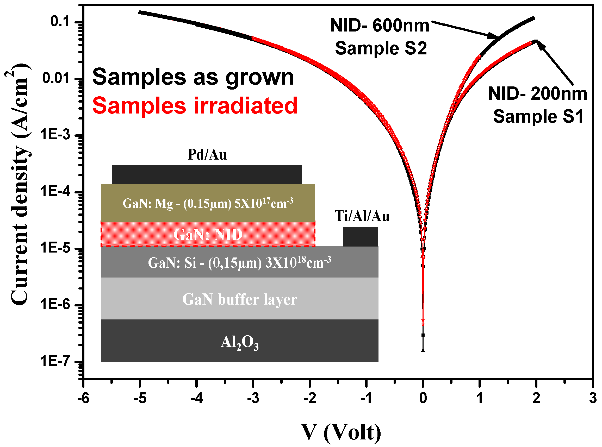
Figure 2 shows the forward and reverse-bias current density–voltage characteristics measured at room temperature for typical S1 and S2 irradiated and un-irradiated samples.
Figure 2.
Semi-logarithmic plots of dark current-voltage (I-V) characteristics of both GaN p-i-n junctions (with two different thicknesses of undoped layer respectively at 200 nm and 600 nm) as-grown and irradiated at room temperature with a diameter of diodes of 1000 µm.
Figure 2.
Semi-logarithmic plots of dark current-voltage (I-V) characteristics of both GaN p-i-n junctions (with two different thicknesses of undoped layer respectively at 200 nm and 600 nm) as-grown and irradiated at room temperature with a diameter of diodes of 1000 µm.
The electrical properties of the diodes were determined from the fit of I-V curves. The value of ideality factor is
n = 5.2, the reverse-bias leakage current at −4 V is 0.09 A/cm
2, these values are the same for both types of samples S1 and S2. The fairly high ideality factor implies that besides thermionic emission, other mechanisms (recombination, tunneling), also contribute to the carriers transport. Regarding the leakage current, it was reported that it occurs through the volume of the device [
5,
6]. From the electrical point of view, as we can see from
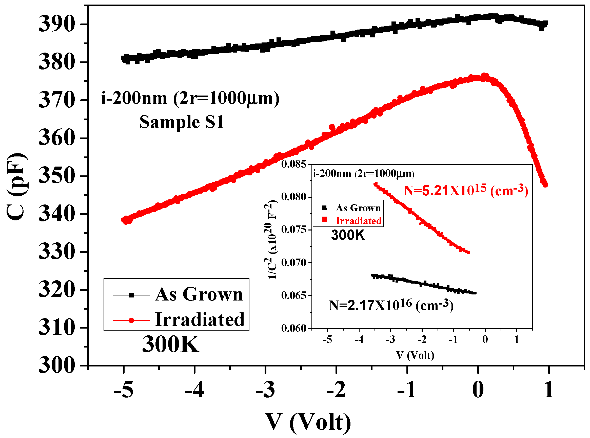
Figure 2, the β-particles irradiation has no effect on the measured parameters for the tested samples. The capacitance voltage (C-V) was performed at room temperature with a frequency of 1 MHz. The measured capacitance for sample S2 has not been plotted, because the measurement revealed no effect of the irradiation (the same value of capacitance). On the other hand, regarding sample S1, a significant effect of β-particles has been observed as illustrated in
Figure 3. A large variation, in the order of 30 pF, is observed in the irradiated sample compared with the as-grown sample where the variation is only 10 pF in the investigated bias range. This result reflects a variation of the free charge density in the depletion region. The reason for this variation is owing to a partial loss of charge carriers in the p-i-n junction upon irradiation. The decrement of the C-V irradiated curve in
Figure 3 can be interpreted as the effects of carrier removal. The formation of traps in the depletion region causes low-energy carriers to be trapped, which reduces the concentration of the free carriers. The inset of
Figure 3 displays the representative 1/C
2-V data of sample S1 measured at 1 MHz. The relation between capacitance and voltage is given by the equation:
where
A is the diode area (cm
2),
d is the thickness of the undoped layer (cm),
Vr is the applied bias (V),
q is the electronic charge (C),
εs is the permittivity (F·cm
−1) of GaN (9.5ε
0),
Vbi is the built-in voltage (V).
Nd and
Na represent the free electron and hole concentration (cm
−3), respectively. We have considered the ratio of (
Na.Nd/Na + Nd) instead of
N. Based on the C-V data of
Figure 3 and the Equation (1), we calculated the thickness of the undoped layer (i-GaN) of the p-i-n junction for both not irradiated and irradiated sample, the thickness is 172 nm and 188 nm, respectively. These values can be compared favorably with the 200 nm thickness of sample S1 given in
Figure 1.
Figure 3.
Typical capacitance-voltage (C-V) measurements performed at 1 MHz of sample S1. The inset shows the 1/C2 versus voltage.
Figure 3.
Typical capacitance-voltage (C-V) measurements performed at 1 MHz of sample S1. The inset shows the 1/C2 versus voltage.
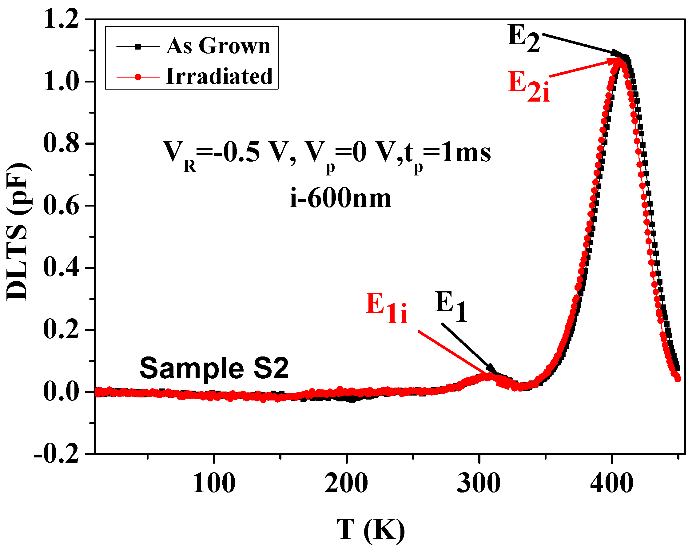
The representative DLTS spectra recorded on sample S2 before and after irradiation are displayed in
Figure 4 with the experimental details reported in the figure caption. DLTS signal spectra revealed the presence of two majority traps E
1 and E
2 at respectively 300 K and 400 K. Their characteristics are listed in
Table 1. Given that the i-side layer of the p-i-n junction is not completely depleted, and the fact that although, non-intentionally doped, it contains excess free electrons, the positive signal indicates that the peaks are correlated with the emission of majority carriers (electron traps). The electron emission rate (s
−1) e
n can be obtained from equation [
7]:
where
σn is the capture cross section for electrons (cm
2),
Vth is the thermal velocity of electrons (cm·s
−1),
Nc the effective density of states at the bottom of conduction band, and
ET is the apparent activation energy of the trap (eV).
Figure 4 unambiguously shows that there is no effect of β-particle irradiation.
Figure 4.
A typical capacitance deep-level transient spectroscopy (DLTS) spectrum recorded for both as grown and irradiated S2 samples with the following parameters: VR = −0.5 V, VP = 0 V and the duration of the filling pulse was tp = 1 ms at rate window 500 s−1.
Figure 4.
A typical capacitance deep-level transient spectroscopy (DLTS) spectrum recorded for both as grown and irradiated S2 samples with the following parameters: VR = −0.5 V, VP = 0 V and the duration of the filling pulse was tp = 1 ms at rate window 500 s−1.
Table 1.
Apparent activation energy, capture cross section, and trap concentration of the defects observed on the sample S1 and S2 as-grown and irradiated. Recording condition: VR = −0.5V, VP = 0V and the duration of the filling pulse was tz = 1 ms.
Table 1.
Apparent activation energy, capture cross section, and trap concentration of the defects observed on the sample S1 and S2 as-grown and irradiated. Recording condition: VR = −0.5V, VP = 0V and the duration of the filling pulse was tz = 1 ms.
| Sample | Level | Activation Energy (eV) | Trap Concentration (cm−3) | Capture Cross Section (cm2) | Origin Identification |
|---|
| S1-As-grown | H1 | 0.83 ± 0.07 | 8.09 × 10¹⁴ | 7.29 × 10⁻¹⁵ | Hole trap |
| S1-Irradiated | H1i | 0.89 ± 0.09 | 2.25 × 10¹⁴ | 5.22 × 10⁻¹⁴ | Hole trap |
| S2-As-grown | E1 | 0.63 ± 0.02 | 1.21 × 10¹⁴ | 1.47 × 10⁻¹³ | Electron trap |
| E2 | 0.81 ± 0.05 | 2.82 × 10¹⁵ | 4.72 × 10⁻¹⁴ | Electron trap |
| S2-Irradiated | E1i | 0.66 ± 0.08 | 1.20 × 10¹⁴ | 8.13 × 10⁻¹³ | Electron trap |
| E2i | 0.78 ± 0.09 | 2.40 × 10¹⁵ | 2.95 × 10⁻¹⁴ | Electron trap |
The Arrhenius plots obtained from the DLTS spectra measured at various temperatures for sample S2 are shown in
Figure 5. From the electrical parameters of the traps, displayed in
Table 1, we can conclude that the similar activation energies derived from these plots confirm that they correspond to the same defect level. The electron trap labeled
E1 and
E1i with thermal activation energy
ET ≈ (0.63–0.66 eV) have signatures very close to the traps commonly observed in undoped and Si doped GaN. Some authors attribute the trap either to a single defect (vacancy) or to V
Ga-O
N complex [
8,
9,
10]. Haase
et al. invoke a native defect in GaN [
11]. Regarding levels
E2 and
E2i, they seem to correspond to the defect levels with activation energy of 0.76 eV reported by Asghar
et al. [
9] and 0.78 eV reported by Auret
et al. [
12]. These defects were observed after irradiating epitaxial
n-GaN with 5.4MeV He ions. The origin is attributed to nitrogen-interstitials (N
i) being produced by the He-bombardment that creates a collisional cascade by displacement of nitrogen atoms from their original crystalline sites to interstitial position. They were also registered for GaN grown under Ga-rich conditions [
13], without any irradiation. Levels
E2 and
E2i, which are identical in terms of the activation energy, are observed in the as-grown and irradiated samples. We may tentatively attribute this level (~0.8 eV) to nitrogen-interstitial (N
i) which are not modified by the relatively low energy irradiation in our case (0.54 MeV).
Figure 5.
Arrhenius plots of the electron traps depicted in
Figure 4 where the DLTS spectra were recorded for sample S2 with the following parameters:
VR = −0.5 V,
VP = 0V and the duration of the filling pulse was
tp = 1 ms at rate window 500 s
−1.
Figure 5.
Arrhenius plots of the electron traps depicted in
Figure 4 where the DLTS spectra were recorded for sample S2 with the following parameters:
VR = −0.5 V,
VP = 0V and the duration of the filling pulse was
tp = 1 ms at rate window 500 s
−1.
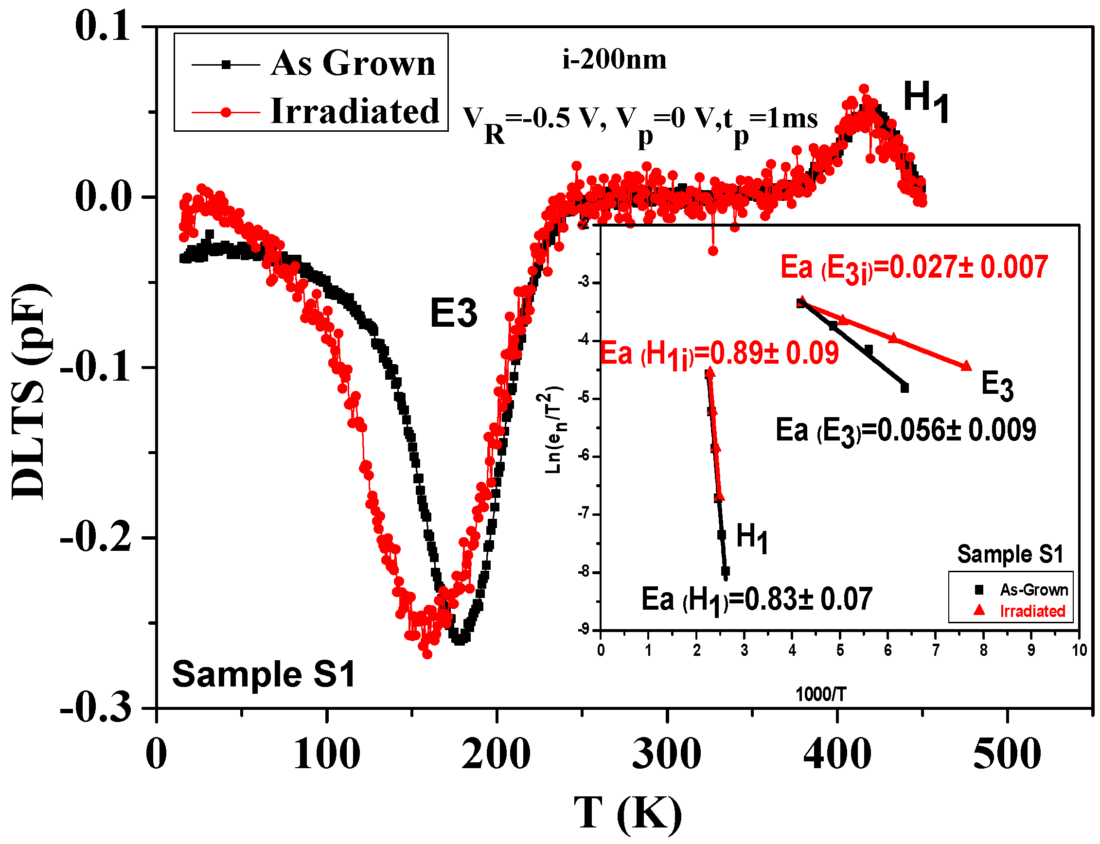
Figure 6 shows DLTS spectra of sample S1 performed under the same conditions as for sample S2. Here the DLTS spectra measured for as-grown and irradiated samples show two distinct peaks: a positive signal labeled
H1 at high temperature (~400 K) and a negative signal labeled
E3 at low temperature (~ 150 K). In the case of sample S1, the i-side layer of the p-i-n junction is completely depleted at −0.5 V. Therefore the active depletion region studied here is mainly on p-type side. Thus, the majority carriers (hole traps) are represented by positive DLTS peaks, and the minority carriers (electron traps) by negative DLTS peaks. The positive signal does not seem to be affected by the irradiation, whereas the negative signal is clearly modified. The Arrhenius plot obtained from the DLTS spectra measured at various temperatures for hole trap is shown in the inset in
Figure 6 and the characteristics displayed in
Table 1. The thermal activation energy
EH1 ≈ 0.83 eV, has a signature very close to the defect level with activation energy of 0.87 eV reported by Emiroglu
et al. [
14]. They attributed the defect to the [V
Ga-(O
N)
3] complex which involves gallium vacancies and oxygen impurity atoms.
Figure 6.
A typical capacitance DLTS spectrum recorded for both as-grown and irradiated sample S1 with the following parameters: VR= −0.5 V, VP = 0 V and the duration of the filling pulse was tp = 1ms at rate window 500 s−1. The inset demonstrates the Arrhenius plots for the detected level H1, H1i, E3 and E3i.
We have seen above that beta particle irradiation has no effect on the deep hole traps. Furthermore it has been mentioned that an electron beam with energy higher than 0.7 MeV is needed to displace gallium atoms [
15]. In our investigation the samples were subjected to electron beam of only 0.54 MeV, which should not generate more gallium vacancies.
Regarding the negative signal shown in
Figure 6, we can clearly see that the Full Width at Half Maximum (FWHM) of black and red peaks are much larger than expected for single point defects. The irradiated sample exhibits both a shift and an increase of FWHM suggesting the creation of a defect with activation energy very close to the one observed in the as-grown sample. We are thus unable to determine the characteristics of the defects
E3 and
E3i. One way of circumventing this difficulty is to record DLTS spectra with lowest rate windows in order to increase their resolution.
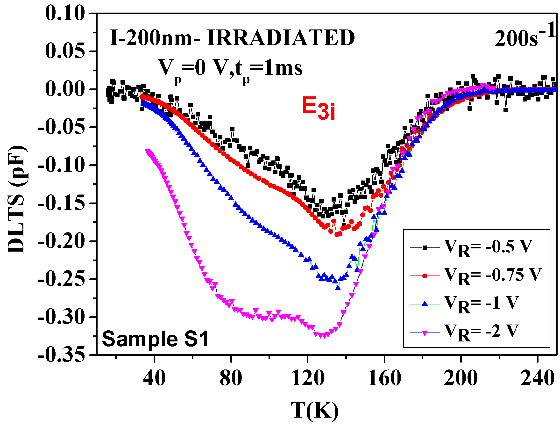
Figure 7 displays spectra recorded with 200 s
−1 at various reverse biases.
As expected we can guess other defects overlapping with the as-grown peaks, although still difficult to bring a decisive discrimination. A detailed study is undertaken with Laplace DLTS [
14], offering a much better resolution, with the hope to come to more conclusive results. At this stage we can only estimate a range of activation energies from the envelopes, rather than peaks, shown in
Figure 6. The levels showing up below this envelope are very likely located in the range 0.06–0.18eV below the conduction band. Levels in this range are commonly observed in
n-GaN grown by either growth techniques (MBE and MOCVD) and assigned to N vacancy (V
N) [
16,
17]. The theoretical study by Van de Walle and Neugebauer [
18] indicated that V
N is a shallow donor. After β-particle irradiation, other unknown defects are created with activation energies in the range mentioned above. These new defects seem to be specific to the p-side of the structure.
Figure 7.
A typical capacitance DLTS spectrum recorded for irradiated sample S1 with the following parameters: VR= [−0.5 V; −0.75 V; −1 V; −2 V], VP = 0 V and the duration of the filling pulse was tp = 1 ms at rate window 200 s−1.
Figure 7.
A typical capacitance DLTS spectrum recorded for irradiated sample S1 with the following parameters: VR= [−0.5 V; −0.75 V; −1 V; −2 V], VP = 0 V and the duration of the filling pulse was tp = 1 ms at rate window 200 s−1.


 ,
, 


