
Beyond the Interconnections: Split Manufacturing in RF Designs

Department of Electrical Engineering and Computer Science, University of Central Florida, 4000 Central Florida Blvd, Orlando, FL 32816, USA
*
Author to whom correspondence should be addressed.
Electronics 2015, 4(3), 541-564; https://doi.org/10.3390/electronics4030541
Submission received: 26 June 2015
/
Revised: 3 August 2015
/
Accepted: 5 August 2015
/
Published: 18 August 2015
(This article belongs to the Special Issue Cyber Security for Embedded Systems: Testing and Protecting Electronic Hardware)
Abstract
:With the globalization of the integrated circuit (IC) design flow of chip fabrication, intellectual property (IP) piracy is becoming the main security threat. While most of the protection methods are dedicated for digital circuits, we are trying to protect radio-frequency (RF) designs. For the first time, we applied the split manufacturing method in RF circuit protection. Three different implementation cases are introduced for security and design overhead tradeoffs, i.e., the removal of the top metal layer, the removal of the top two metal layers and the design obfuscation dedicated to RF circuits. We also developed a quantitative security evaluation method to measure the protection level of RF designs under split manufacturing. Finally, a simple Class AB power amplifier and a more sophisticated Class E power amplifier are used for the demonstration through which we prove that: (1) the removal of top metal layer or the top two metal layers can provide high-level protection for RF circuits with a lower request to domestic foundries; (2) the design obfuscation method provides the highest level of circuit protection, though at the cost of design overhead; and (3) split manufacturing may be more suitable for RF designs than for digital circuits, and it can effectively reduce IP piracy in untrusted off-shore foundries.
1. Introduction
The globalization of integrated circuit (IC) supply chains, especially the outsourcing of chip fabrication and the integration of third-party intellectual property (IP) cores, breeds security concerns and makes it easier to compromise the once trusted IC development process [1,2]. Among all security threats, malicious logic insertions (also known as hardware Trojan attacks) and IC piracy are the most critical security threats that the U.S. government is facing as more domestic IC companies go fabless. Following the trend of the growth of the merchant foundry industry, fabless IC design houses can have access to reasonably-priced advanced-process capacity without the need for huge capital expenditure (the cost of developing a semiconductor foundry will be over $5.0 billion by 2015 [3]). The reduced fabrication cost, at the same time, sacrifices design security and leaves all IC designs in the hands of the foundry. The International Chamber of Commerce (ICC) stated in their 2011 report that the total global economic and social impact of counterfeit and pirated products is valued at $775 billion every year. The figure is estimated to more than double to $1.7 trillion by 2015.
For this reason, both governmental agencies and industrial companies are looking for a balance between fabrication cost and design security to prevent foundries from learning the design details of submitted design layouts. In order to address such threats, various hardware Trojan detection methods and hardware metering methods have been developed [4,5,6]. Among these approaches, design obfuscation and camouflaging are candidates; however, both methods require modification of the original circuits, which may cause a performance overhead. Intelligence Advanced Research Projects Activity (IARPA) proposed a new methodology called split manufacturing, which only adds trivial efforts to IC designers, but is able to effectively prevent IC piracy [7]. The key idea of split manufacturing is to protect circuit/system designs by dividing the manufacturing chips into front-end-of-line (FEOL), consisting of transistor layers to be fabricated by off-shore foundries, and back-end-of-line (BEOL), consisting of metallizations to be fabricated by trusted domestic facilities. Through this divided fabrication procedure, the design intention is not fully disclosed to the FEOL foundry. Even though the concept is straightforward, a successful implementation requires further research on various aspects, especially the balance between cost and security when the designer splits the layout into FEOL and BEOL. Analytical and experimental results have already been presented for digital circuits [8,9,10,11,12,13,14,15]. However, the analog/RF designs are rarely discussed when using split manufacturing, even though analog/RF circuits are more likely to be IP piracy victims than their digital counterparts.
In fact, the fundamental difference between digital design flow and the RF design process has already raised concerns as to whether it is still applicable to apply split manufacturing in RF design. A deeper look into both design flows proves that it would be more suitable to apply split manufacturing in RF circuits than in digital circuits, because of the unique functionality metal layers play in RF designs: (1) metal layers are solely used as interconnections between gates and modules in digital circuits, while in RF circuits, metal layers are also used to build functional blocks (e.g., inductors are often located on the top metal layer; capacitors are built in upper level metal layers); and (2) while metal layers are abstracted as wire connections in digital designs, wire length and wire direction are both functional parameters in RF designs. Therefore, a foundry fabricating the FEOL part of digital circuits may face a mathematical problem with finite solutions in order to recover the whole functionality of the design (note that the possible solution space could be large given the large amount of standard cells in digital circuits; in fact, this is the key criterion to evaluate the security level of the split manufacturing method in digital circuits). On the other hand, the foundry of RF FEOL would need to explore an infinite solution space to recover the RF design.
Based on the above discussion, it becomes obvious that split manufacturing should be more effective to protect RF circuits from IP piracy. To assess our claim, analytical calculation and experimental demonstrations are performed in this paper to solidify our findings and to push the territory of split manufacturing to cover all types of circuit designs.
The rest of the paper is organized as follows: Section 2 introduces the state-of-the-art split manufacturing practices. Section 3 presents the RF design flow and theoretical analysis of the power amplifier. A detailed analytical analysis of applying split manufacturing in RF designs is presented in Section 4. To assess the analytical results, experimentation on a fabricated power amplifier is performed in Section 5. Finally, the conclusions are drawn in Section 7.
2. Split Manufacturing in the Digital Domain
The concept of split manufacturing was officially proposed by the Intelligence Advanced Research Projects Activity (IARPA) through the Trusted Integrated Chips (TIC) program. The new program aims to develop and demonstrate new split manufacturing for chip fabrication where security and intellectual property protection can be assured [7]. Since the program’s commencement, a few embodiments of split manufacturing in digital circuits have been proposed. Imeson et al. proposed a method by applying 3D integration technology in split fabrication. Using a through silicon via (TSV), they came up with a security algorithm from the graph problem to obfuscate the circuit by lifting certain wires to a trusted tier [9]. Rajendran et al. examined a split fabrication after the metal3layer, where digital benchmark circuits are separated into several partitions without interconnections [8]. Since the connections within each gate are mostly located in the metal1 and metal2layers, which are known to the FEOL foundry, they further proposed a fault-analysis-based pin swapping algorithm to defend the common proximity attacks. More recently, Vaidyanathan et al. investigated the feasibility of split fabrication after the metal1 layer, so that untrusted foundries only have the information of basic gate-level blocks [11]. A similar technique is then applied to digital/analog IP designs [12]. A defense strategy against recognition attacks on IPs and an obfuscation method were both proposed, as well as experimental demonstrations on a 1-KB SRAM and a 14-bit current steering digital-to-analog converter (DAC).Jagasivamani et al. examined several front-end obfuscation techniques, information theory metrics and impacts on performance penalties [13]. They applied their techniques in mult24and a5/1to present a statistical analysis of the performance yield when filling the standard cells in spared space in a complex digital design. The method of split manufacturing is further expanded to the application of reliable attack detection with test-only BEOL [14].
Hill et al. examined the idea of employing split manufacturing in the design of asynchronous FPGAs [10]. They described a comparative study of an asynchronous FPGAs manufactured in both a standard process and a split manufacturing process. Compared to the standard process, the split manufacturing process suffers penalties either on operating frequency or on the energy consumption.
3. RF Design Flow
Thanks to the advanced EDAtools for RF circuit designs and the development of RF design kits, RF engineers have become more productive than ever before. Nevertheless, a typical RF design still involves the heavy work of design fine-tuning, and the designers’ experience plays a critical role here [16,17]. Figure 1 shows the steps of a modern RF design flow.
Figure 1.
Standard RF circuit design flow.
3.1. RF Design Procedures
From Figure 1, we can see that Steps I–III are the preparation of the RF circuit specification. Taking a power amplifier as an example, the defined specification will include design information, such as the delivered output power, the amount of circuit stages, the operation class, etc. Different from digital designs where the specification is strictly followed, the specification for RF circuits only serves as a guideline, as it often happens that the performance of the final design deviates from the original settings (experienced RF engineers may be able to narrow the performance gap, which is why experienced RF designers are valued).
Guided by the specification, the circuit schematic will be designed, simulated and optimized. The optimized schematic will then guide the work of layout design and post-layout simulation. All physical-level parameters come into the map during the layout design and post-layout simulation, such as parasitic capacitors, wire resistance, etc. For RF circuits, the parasitic components can significantly affect the design performance and significantly cause the deviation of the circuit performance from the schematic level simulation. Therefore, a large portion of the design time will be spent in layout optimization and circuit fine-tuning, even for experienced designers. If the circuit passes the post-layout simulation, it will be sent to the foundry for fabrication and for post-fabrication testing. Even though current foundries embrace advanced technology and delicate equipment, the parasitics introduced by the fabrication process remain a problem, i.e., unpredictable parasitic resistance and capacitance during the fabrication will affect both circuit functionality and performance. A fabricated RFIC circuit may not work properly, which increases the demand for further tuning and trimming. To lower the fabrication cost and to increase the yield rate, techniques of post-fabrication calibration are used in modern RF designs, e.g., knob adjustments and transverse electromagnetic (TEM) cells.
3.2. Power Amplifier Modeling and Analysis
Power amplifiers are among the most widely-used RF devices and are installed in almost every electronic device. For instance, power amplifiers serve as the very front end of transmitters in broadcasting systems and are used in audio systems to increase and decrease the volume. The basic functionality of a power amplifier can be described as an augmentation to the system power level. Therefore, being one of the most important tasks in RF design, researchers are dedicated to designing highly-efficient and robust power amplifiers. For example, the quality of a power amplifier design decides whether or not a wireless transmission signal can be well detected by wireless receivers or not. For this reason, we chose the power amplifier as the example in the rest of this paper when we demonstrate how the split manufacturing can help improve design security and prevent IP piracy for RF circuits.
Besides the experimental design flow shown in Figure 1, analytical equations also play critical roles to help designers derive the approximate range of the component sizes from the specification. Since most power amplifiers use N-type MOSFET, the drain current for N-type MOSFET in the saturation region is revisited in the following equations:
where
is the electron mobility,
is the threshold voltage,
is the oxide capacitance per unit area, W is the channel width, L is the channel length,
is the gate-source voltage of the MOSFET and λ is the channel length modulation factor. Equation (2) presents the expression of threshold voltage, an important parameter in CMOS designs, where γ is the body effect constant,
is the substrate Fermi potential and
is the source-to-body voltage. Since the inputs of power amplifiers are often nonlinear signals with DC biasing, particularly sinusoidal waves, the drain current in a power amplifier is shown in Equation (3), where
is the amplitude of the AC component of the drain current and ω is the resonant frequency.
Equations (1)–(3) determine the operation mode of the power amplifier, because different DC biasing and operating frequency would cause different conduction angles. Note that the determination of the operation mode guides the entire design flow. For instance, Class A power amplifiers need to constantly turn on the transistor all of the time, which means drain current should always be larger than zero. On the other hand, Class B power amplifiers require the operation on a 50% duty cycle, where transistors are turned off for a half cycle. The typical characteristics of power amplifiers include the output power and the power-added efficiency, whose calculations are listed below:
In the above equations,
is the conjugate input current,
is the conjugate output current and
is the DC power dissipation. Even though there are other reference parameters needed in power amplifiers, the output power and the power-added efficiency are the two key parameters for power amplifier evaluation. The attacker, who is assumed to be an experienced RF designer, should be aware of those equations, as well, and will apply them in an RF circuit recovery from FEOL. However, it is noteworthy that unlike digital design, those equations can merely determine a reasonable range of design, and the final results are derived after plenty of tuning and trimming work. In this paper, we will evaluate the PA performance within these two parameters to demonstrate the application of split fabrication in RF circuits and to evaluate the security level.
4. Split Manufacturing in RF Circuits
As we mentioned earlier, the removal of metal layers in RF circuits will not just hide the interconnections between circuit components, but also eliminate the passive components, which are built in metal layers. Since a typical RF circuit only includes very few transistors and other passive components, the recovery of interconnections between these components will not be a difficult task. Rather, being able to derive the missing passive components and their sizes would be the main advantage of applying split manufacturing in RF designs. For the same reason, the difficulty level for attackers with the FEOL at hand to recover the passive components and to guess the sizes of these passive components will be the key criteria to assess the effectiveness of split manufacturing application in RF designs.
Compared to digital split fabrication [8], where the proximity attack dominates the security analysis, routing and mapping are no longer an issue for RF circuits. Furthermore, the recognition attack mechanism used in [12] cannot accurately explain the issue with RF split fabrication. To better guide the implementation of split manufacturing in RF circuits and to balance between the security level and design efforts, we propose three approaches/scenarios to perform the RF split fabrication:
- Scenario I: Remove only the top metal layer from the layers to generate FEOL. Since the inductors are often located in the top layer, the FEOL foundry does not have the information of interconnections through the top metal layer, as well as the inductor locations and sizes.
- Scenario II: Remove both the top and the second from the top metal layers. In this scenario, two upper metal layers are removed so that both inductors and capacitors are missing from the FEOL layout, because the capacitors are often built through the top two metal layers.
- Scenario III: Design obfuscation. For RF designs, inductors are always located in metal rings, and lower metal layers will be removed inside the rings for performance optimization. Therefore, the rings themselves, which contain multiple metal layers, would indicate the positions and approximate sizes of inductors. Similarly, the lower metal layers will not be used where capacitors are located. Therefore, attackers in both Scenarios I and II may learn the precise positions of the removed inductors/capacitors and may even further estimate their sizes. To further increase the security level, but still avoid performance overhead, we propose an obfuscation technique during the design phase to insert non-functional rings and to create empty zones in the original design. Using this method, it becomes more difficult for attackers to pin down the location, the count and the sizes of passive components.
For the demonstration purpose, the TSMC 0.18 μm technology supporting six metal layers is used. In both analytical and experimental demonstrations, Scenario I indicates the removal of metal6 layers. Similarly, Scenario II indicates the removal of the metal5 and metal6 layers. Scenario III follows the same rules that new rings and empty zones are removed from the metal layers metal1 to metal4. Note that the proposed three scenarios can be applied to any other process technology with the adjustment of available metal layers.
4.1. The First Example
To demonstrate all three application scenarios, as well as their security levels, a single-stage single-transistor Class AB power amplifier is investigated as our first example where we assume that the inductor is using the metal6 layer and the capacitors are using metal5 and metal6 layers [18]. A more sophisticated example with detailed layout information will be introduced in Section 5.
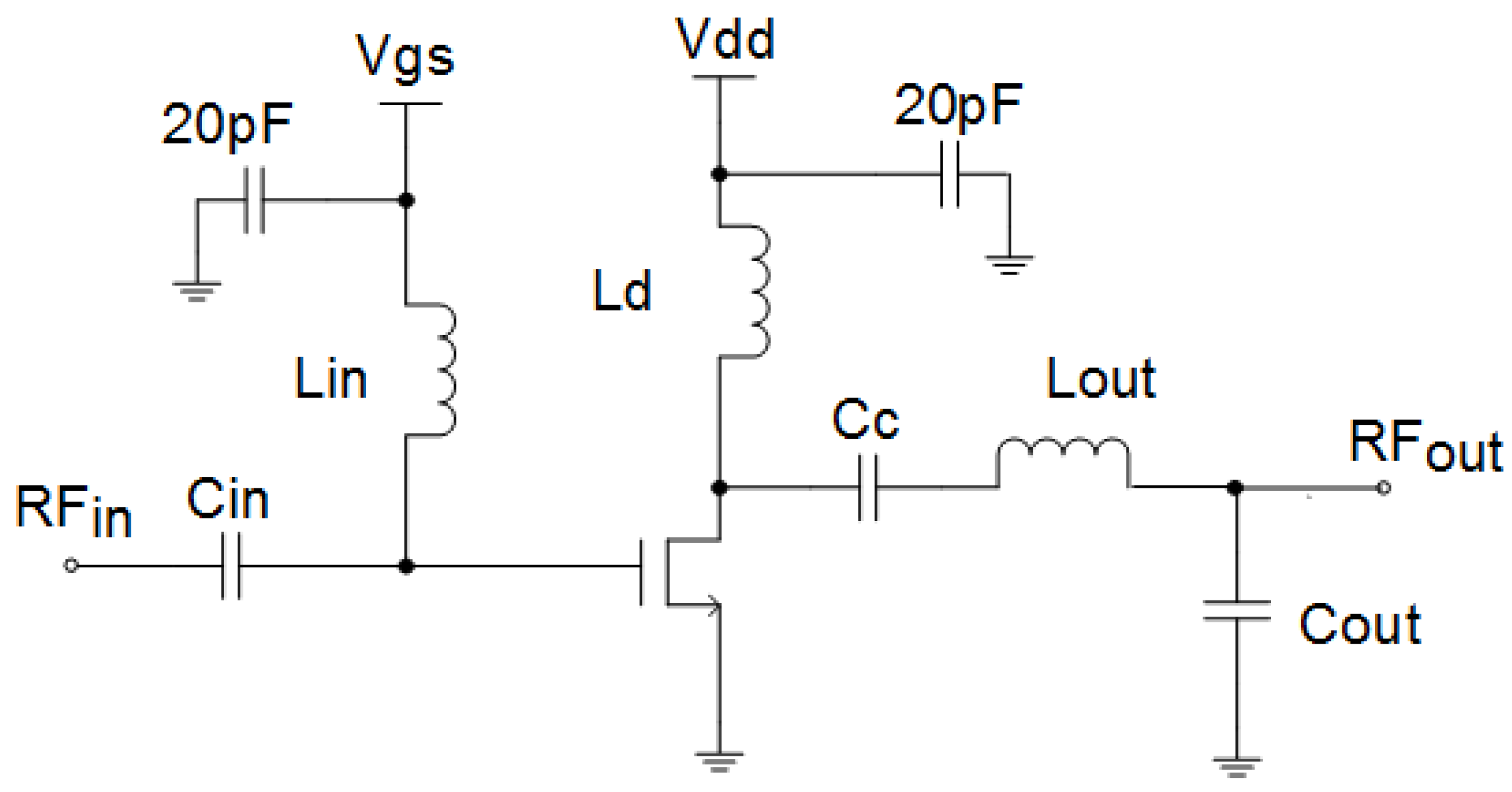
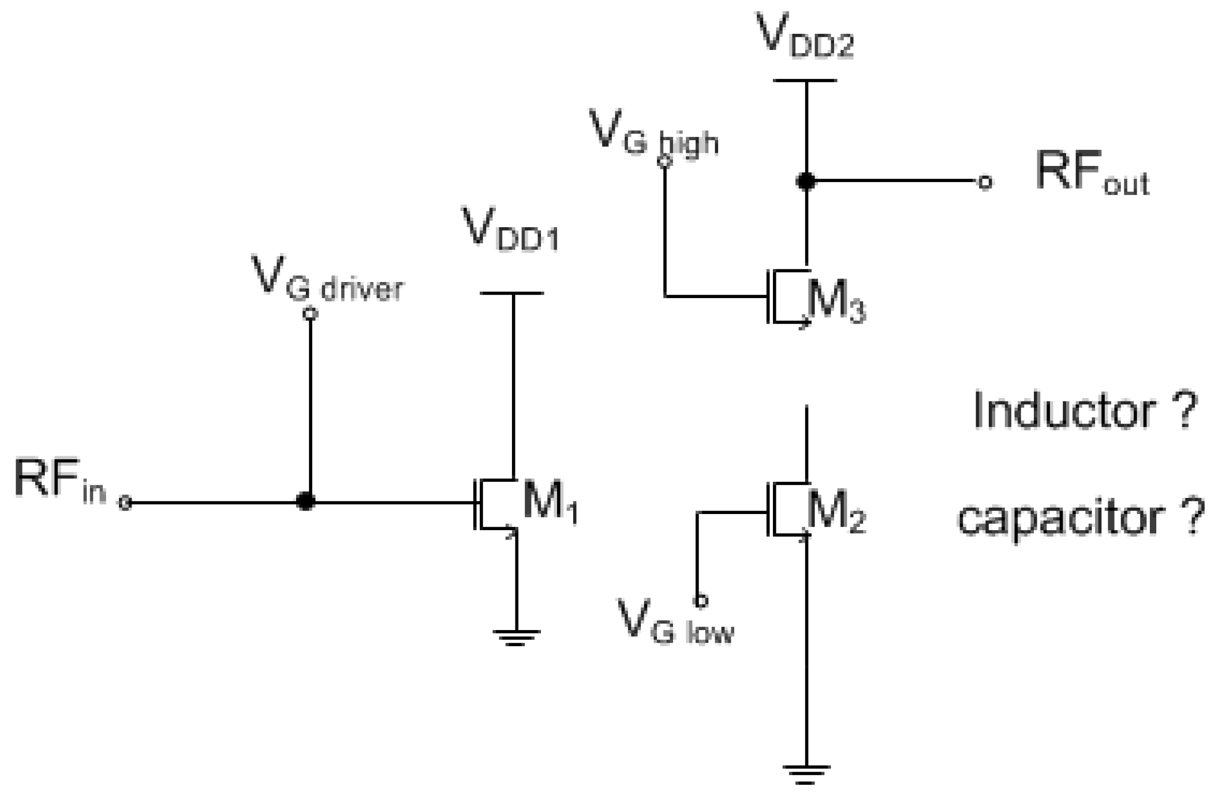
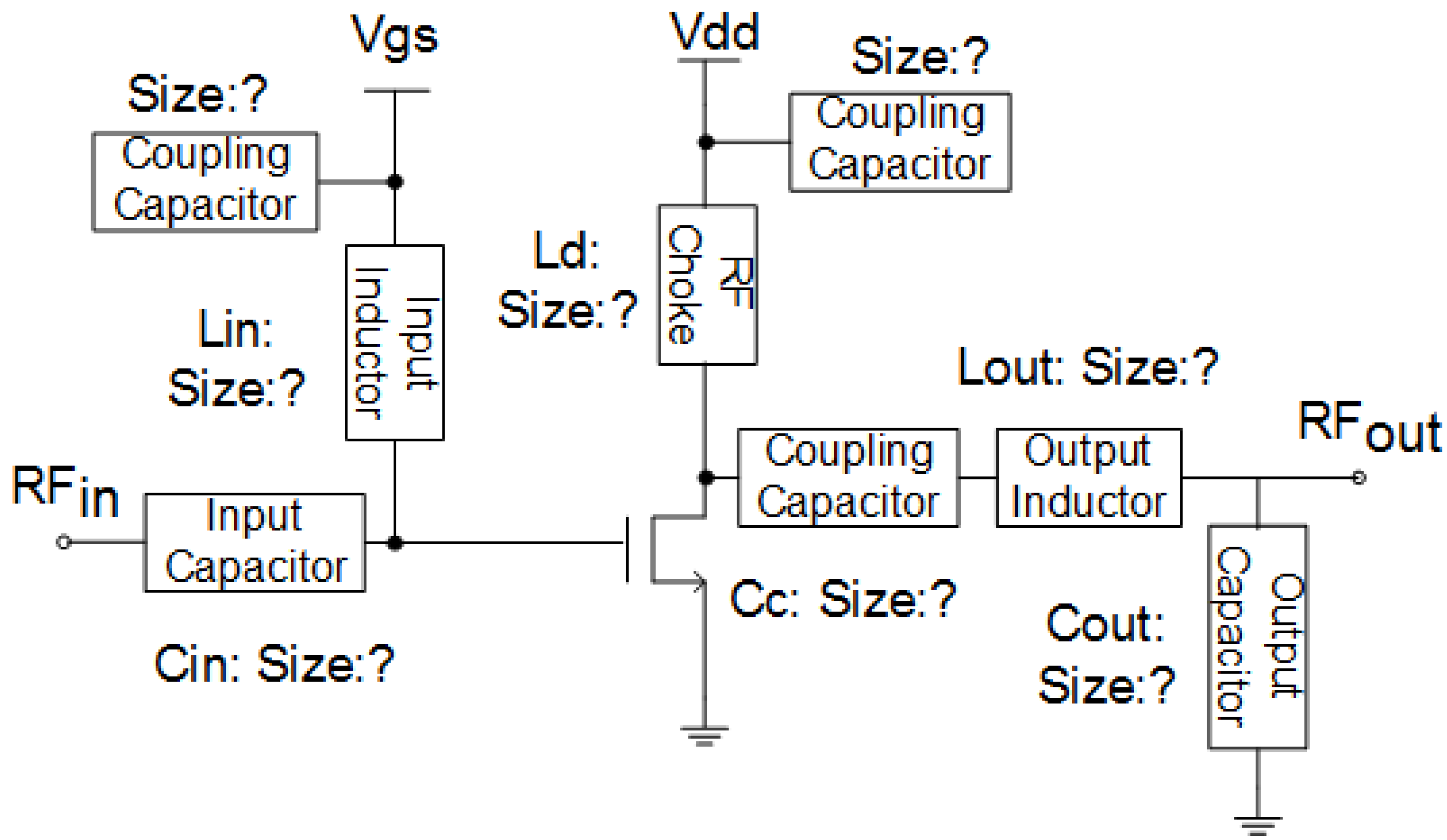
The Class AB power amplifier (see Figure 2 for a detailed schematic) works at 5.8 GHz with a low supply voltage of 1.9 V. It is designed to deliver 19.8 dBm output power and 28.1% power-added efficiency.
Figure 2.
Schematic of a Class AB power amplifier.

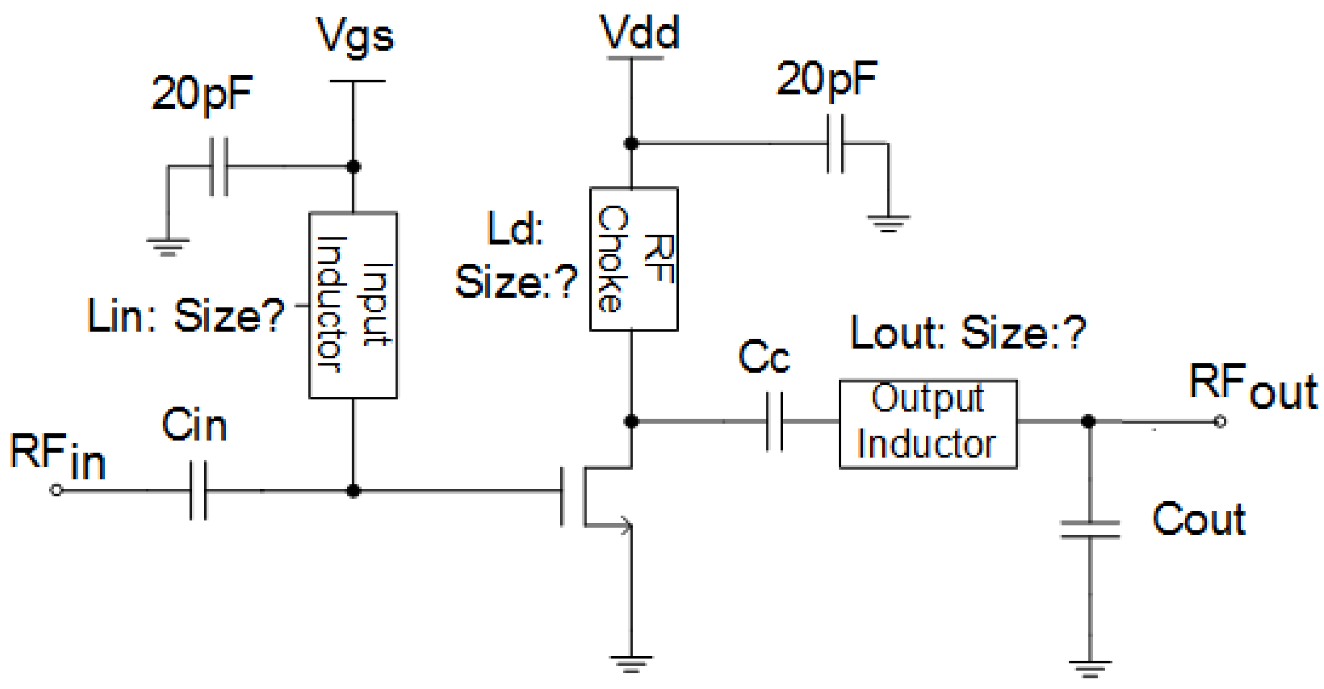
4.1.1. Scenario I: Removal of Metal6 Layers (Inductors)
Since metal6 is removed from the FEOL, the schematic of the Class AB power amplifier, shown in Figure 3, is missing all inductor information. Although the attackers can easily recover the count and the locations of all inductors, they do not know the exact sizes and the values of the inductors. More specifically, the attackers can learn that three inductors are used in the design through the inductor rings. They can also extract the values for all other components. Therefore, the attackers with the FEOL of the power amplifier at hand can easily guess the general functionality of the entire design. However, a detailed specification, including the supply voltage and the operating frequency, remains unknown. As a result, the task for attackers to recover the entire circuit is not as simple as sweeping all possible inductor values. As we emphasized earlier, we assume that the attackers are also experienced RF designers, so they would also apply the analytical calculation based on Equations (1)–(6) and other parameters from the known components in order to derive the inductor values. The procedure to recover the whole circuit from the known FEOL by attackers is described in the following steps (note that the IP piracy cost is directly related to the complexity of these steps):
Figure 3.
A Class AB power amplifier with metal6 removed (missing inductors).

Step 1: In the first step, the attackers will try to find out the operating condition,s such as bias voltage, supply voltage and operating frequency, which can significantly shift the power amplifier performance. Since the untrusted foundry is also the provider of the fabrication process (in our case, we are using the 0.18-μm technology), the attackers should be aware of the available supply voltage for this technology (from 1–3.3 V). The attackers should try at least 23 different supply voltages if a step size of 0.1 V is chosen (they may try more supply voltages with a smaller voltage step size in order to get more accurate simulation results). In terms of gate biasing, the reasonable range for a power amplifier varies from 0.4–1 V; however, it is not necessary that all designs follow this setting (e.g., an exception will be presented in the Experimentation Section). Hence, using 0.05 V as a voltage sweeping step, the gate biasing can have at least 13 different cases for attackers to choose. Meanwhile, the operating frequency still remains a puzzle to attackers, which acts as an imperative role in RF design. The attackers may narrow down the spectrum by assuming this example design works in the commercial communication protocol range, which basically ranges from 0.8–6 GHz. Again, the design may or may not take the communication frequency as its operating frequency, because the attackers are not aware if this layout works for some specific applications, either military or scientific confidentiality. Under this assumption, it comes to a group of 53 possible values if a step of 0.1 GHz is selected.
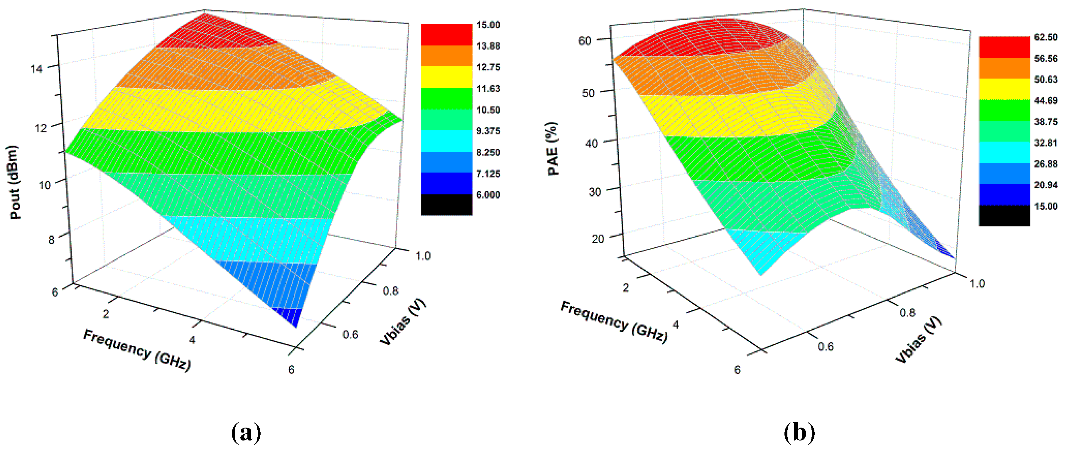
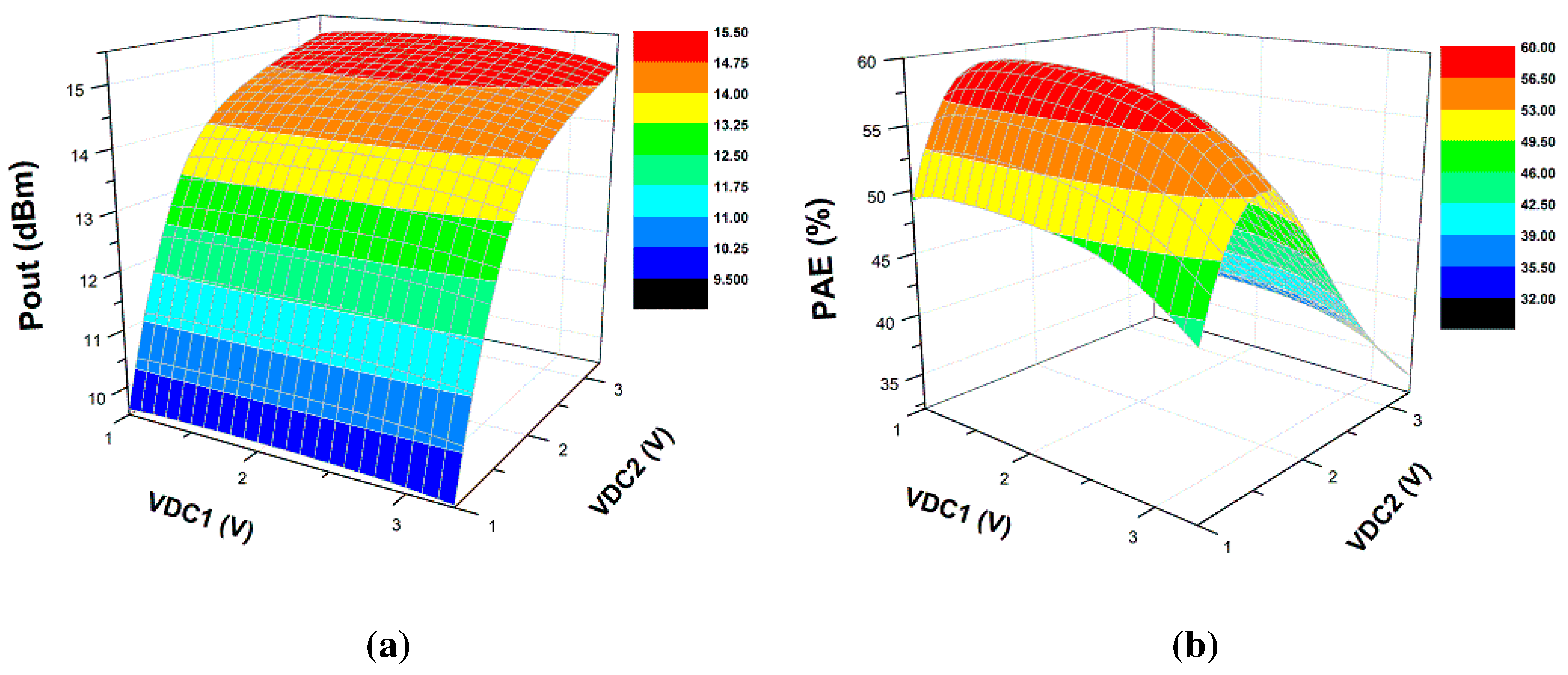
With all of these possible cases available, the attackers will then run simulations to recover the original design by choosing the result with the best output power and power-added efficiency. For example, Figure 4a,b show the case that the actual supply voltage and gate bias, namely 1.9 and 1 V, do not deliver the best output yields. Similarly, Figure 5a,b show that the maximum output power is not coincident with the maximum power-added efficiency. Since this power amplifier is designed for low-power applications, the specification defines the operating frequency to be 5.8 GHz; however, Figure 5 shows that the defined operating frequency is located in the middle level of the overall performance. Clearly attackers cannot recover the original design if the optimized parameter settings are chosen. Figure 6a,b reflects the relationship of circuit performance versus frequency and gate bias. As shown in the figure, the actual values for frequency and gate bias, 5.8 GHz and 1 V, are located in the low performance area. Therefore, if the attackers follow the recovery process through Figure 4, Figure 5 and Figure 6, they cannot find the correct settings. Note that this sample testing process only represents a small fraction of the overall testing space, meaning that it will take a significant amount of time for attackers to fully simulate the design and to collect the original design parameters, even for a simple RF circuit.
Figure 4.
(a) Supply voltage and gate biasing versus output power; (b) supply voltage and gate biasing versus power-added efficiency.
Figure 4.
(a) Supply voltage and gate biasing versus output power; (b) supply voltage and gate biasing versus power-added efficiency.
Figure 5.
(a) Supply voltage and frequency versus output power; (b) supply voltage and frequency versus power-added efficiency.
Figure 5.
(a) Supply voltage and frequency versus output power; (b) supply voltage and frequency versus power-added efficiency.
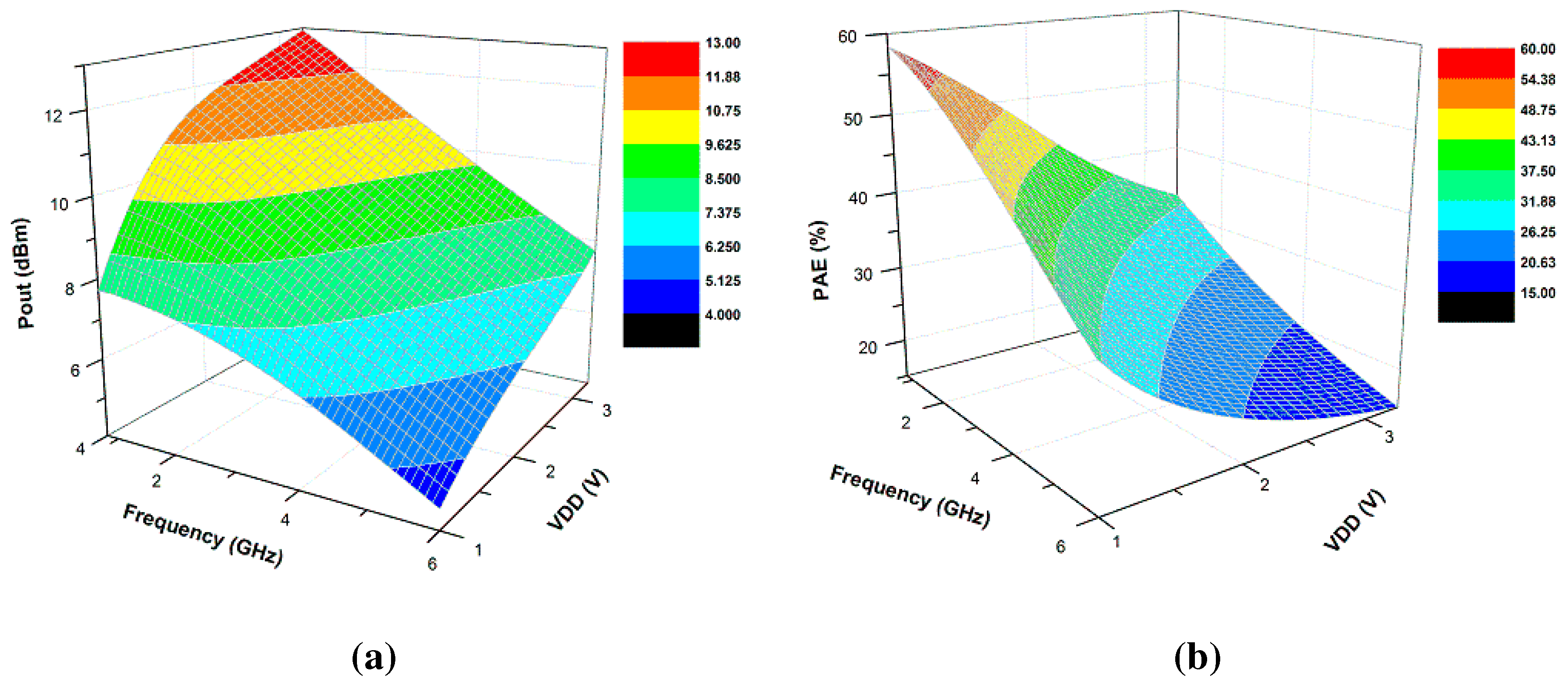
Figure 6.
(a) Gate biasing and frequency versus output power; (b) gate biasing and frequency versus power-added efficiency.
Figure 6.
(a) Gate biasing and frequency versus output power; (b) gate biasing and frequency versus power-added efficiency.

Step 2: In the second step, we assume that the attackers have chosen the correct operating conditions for the power amplifier; next, they need to set the biasing conditions to precisely recover the inductor values. Following a general RF design methodology, the experienced attackers will sweep the RF choke
and the input inductor
by a reasonable range, which is from 0.5–3 nH in the 0.18-μm technology, to check the input reflection coefficient S11 and to further guess the frequency range, rather than a random sweeping on different frequencies. Based on the simulation results, the attackers will probably learn the circuit working frequency between 4 and 7 GHz. The derived frequency range helps to narrow the possible range of the input inductor; however, the attackers need to select the inductor value for a 4–7-GHz design operation. The attackers will then sweep the RF choke
and the output inductor
to optimize the output performance and the matching network. The simulation results will be meaningless if a wrong input inductor value is chosen.
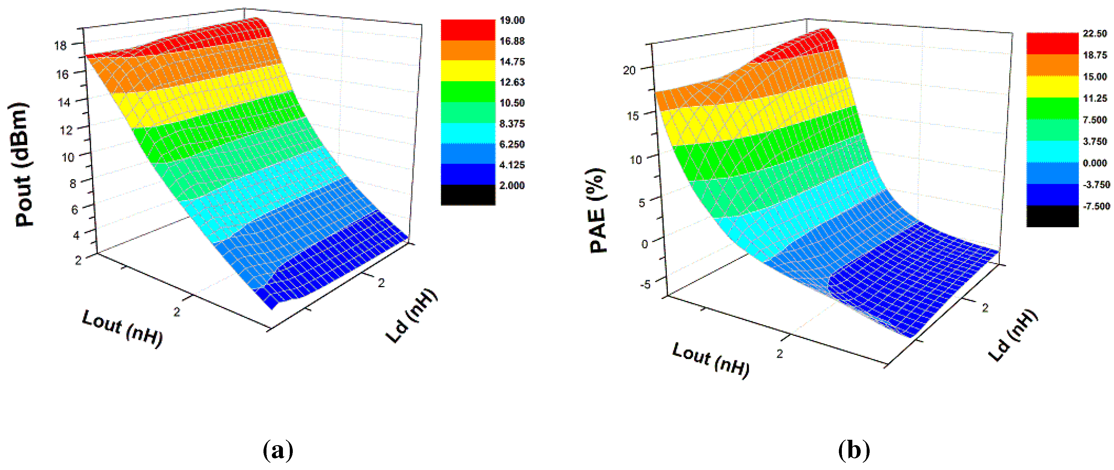
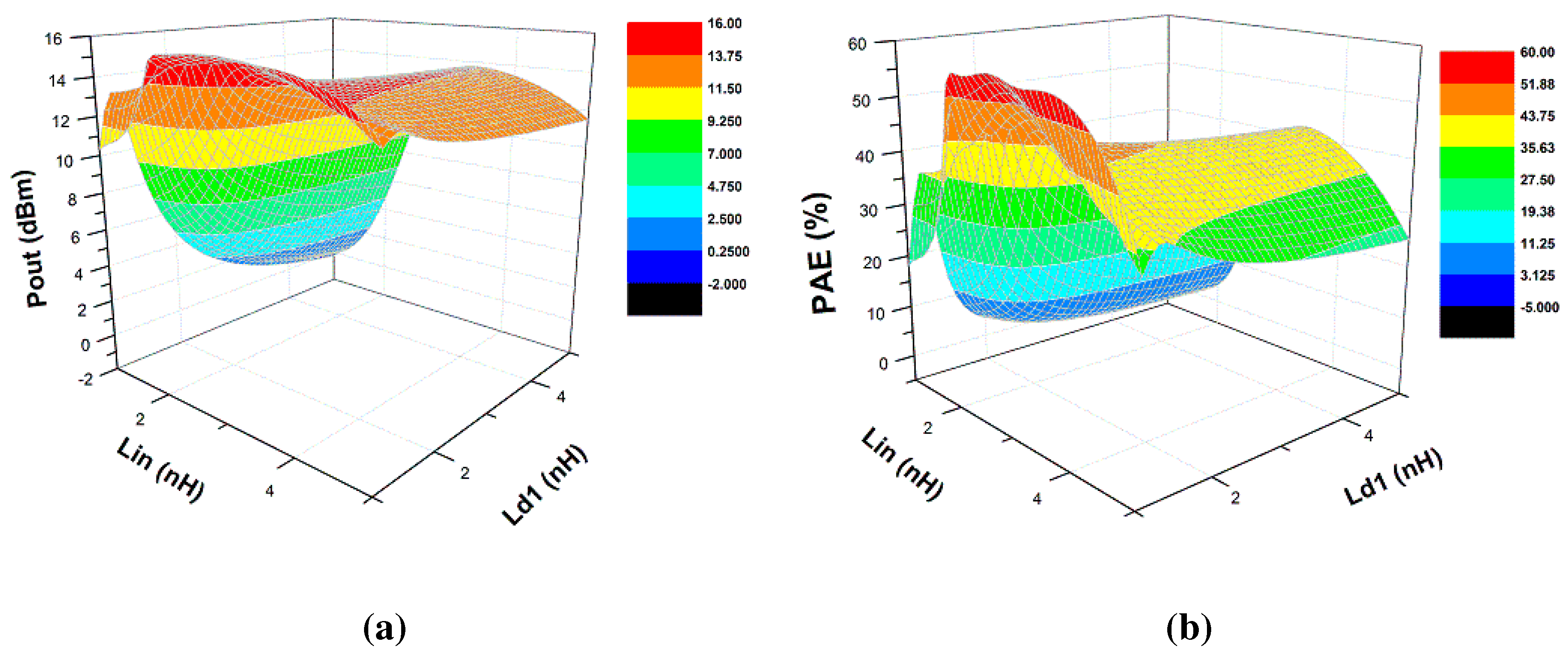
Figure 7 illustrates the output results that vary with respect to the RF choke and the output inductor. The actual values for the RF choke and the output inductor are 963 and 670 pH, respectively. However, from Figure 7, we can see that both values produce good, but not the best performance. It is possible that the attackers only aim for the best performance, so they may choose inductor values from the wrong range.
4.1.2. Scenario II: Removal of Metal5 and Metal6 Layers (Capacitors and Inductors)
In this case, both inductors and capacitors are not available to the untrusted foundry because of the removal of the metal5 and metal6 layers from the FEOL in Figure 8. The missing capacitors add additional uncertainty, which makes it difficult for attackers to recover the whole design. That is, the unknown capacitors add more freedom in the simulation though parameter sweepings and will produce large amounts of combinations of inductors and capacitors. In this case, it is much easier for an experienced attacker to follow the typical power amplifier design procedure to retrieve the missing components.
Figure 7.
(a) Output inductor and RF choke versus output power; (b) output inductor and RF choke versus power-added efficiency.
Figure 7.
(a) Output inductor and RF choke versus output power; (b) output inductor and RF choke versus power-added efficiency.

Figure 8.
Schematic of the Class AB power amplifier without the top two metal layers (missing inductors and capacitors).
Figure 8.
Schematic of the Class AB power amplifier without the top two metal layers (missing inductors and capacitors).
Step 1: The first step of circuit testing is exactly the same as that in Scenario I.
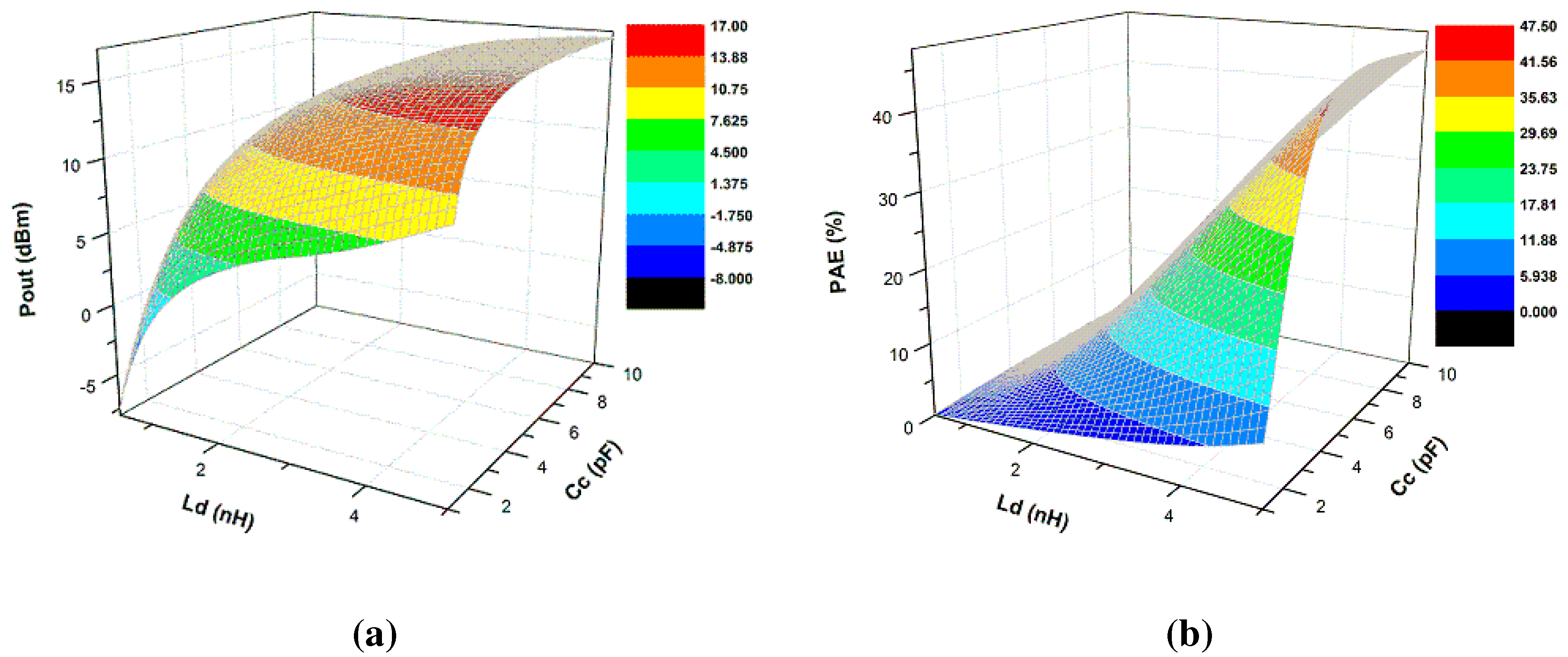
Step 2: After selecting the operating point, the attacker needs to figure out the RF choke inductor and output coupling capacitor. The 0.18-μm technology indicates that the reasonable ranges for inductor and capacitor are 0.5–5 nH and 1–10 pF, respectively. Using a sweeping step of 0.1 nH and 0.1 pF for inductors and capacitors, respectively, the attackers will come up with a total of 45 possible values for inductors and 90 possible values for capacitors (note that the range of inductor shifts from 0.5 to 5 nH rather than from 0.5 to 3 nH due to the fact that capacitor values are unknown in Scenario II). Figure 9 shows the overall circuit performance when the values of the choke inductor and the output capacitor are changing. The figure helps attackers to recover the correct values of both components.
Figure 9.
(a) RF choke and output coupling versus output power; (b) RF choke and output coupling versus power-added efficiency.
Figure 9.
(a) RF choke and output coupling versus output power; (b) RF choke and output coupling versus power-added efficiency.
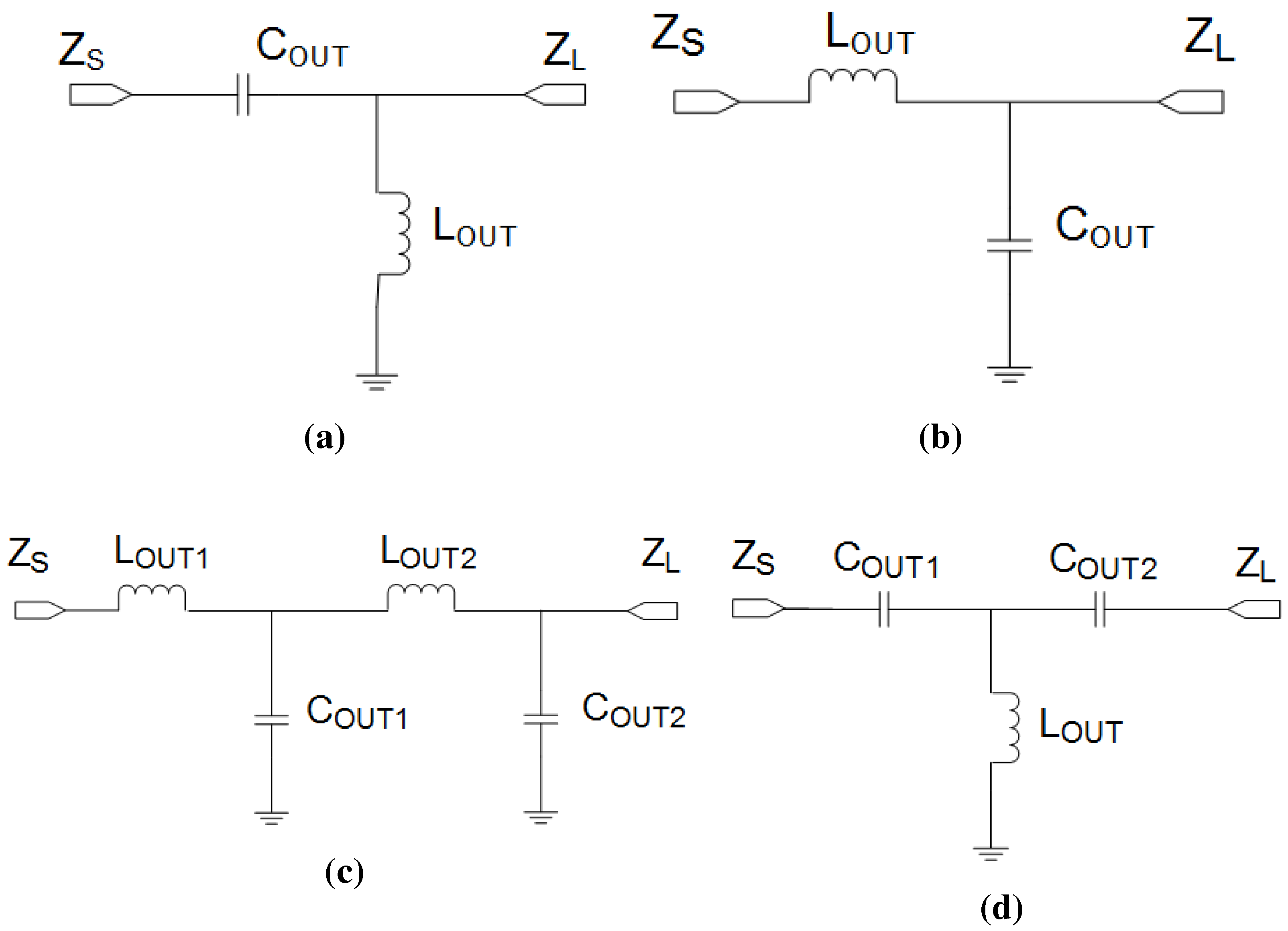
Step 3: After selecting the RF choke and coupling capacitor from various combinations, the attackers need to perform output matching to achieve a matched 50 Ω output. RF designers often perform output matching through load pull simulation, which provides the designers a bunch of matching combinations to choose from. Advanced EDA tools can help synthesize the maximum output power and power-added efficiency, as well as further reflect the impedance of the optimal points. After choosing the impedance, the designers can use the Smith chart to recover the output matching network. Due to the simple structure of the single transistor power amplifier, the output matching network only includes one inductor and one capacitor. Relying on the load pull simulation, the attackers can retrieve four possible matching networks, as shown in Figure 10.
The possible topologies cover L-type (Figure 10a,b), Π-type (Figure 10c) and T-type (Figure 10d), which are all basic network topologies in RF design. All component values for each topology are located in reasonable design ranges; however, only the first two networks are possible given the number of passive components.
Step 4: After the load pull simulation, the attackers need to use the source pull simulation to recover the input matching network, which follows a similar procedure to the load pull simulation.
Step 5: The final tuning is necessary for attackers to adjust the performance before all circuit parameters are recovered.
4.1.3. Scenario III: Obfuscation Techniques
Although various obfuscation techniques can be applied that increase the difficulty for attackers to recover the original circuit, in order to balance the performance impact and lower the design cost, only two obfuscation methods are demonstrated in this paper. Those two methods add (1) extra block space where the capacitors/inductors are located and (2) dummy cells to mislead the attackers into incorrect simulations.
To avoid high frequency signals interfering with each other, the lower level metals are not used where the inductors/capacitors are located. The existence of these empty areas may reveal the approximate sizes of the inductors/capacitors, which can lead to the recovery of the original design. To address this issue and to further increase the difficulty of RF IP piracy, we propose an obfuscation technique to deliberately increase the passive component area. This will have the effect of lowering the correlation between the area of each inductor/capacitor and their value.
Figure 10.
Four possible output matching networks for the Class AB power amplifier.

A second method will also be applied, which includes unused empty blocks in the original design, so that the attackers are unable to find the correct circuit structure. Those extra blocks can be located either in the input or the output side. For example, the attackers will only select L-type output matching networks from Figure 10a,b, but they will also consider other topologies if two empty blocks are inserted.
Different from the IP protection Scenarios I and II, the obfuscation technique in Scenario III requires modifying the original layout. The RF design performance will be affected due to the sensitivity of layout modifications. To address this issue, we suggest a new RF design methodology, called security co-design, which considers security at the early stage of the RF designs by altering some design rules to integrate the obfuscation technique in the design flow.
5. Experimentation
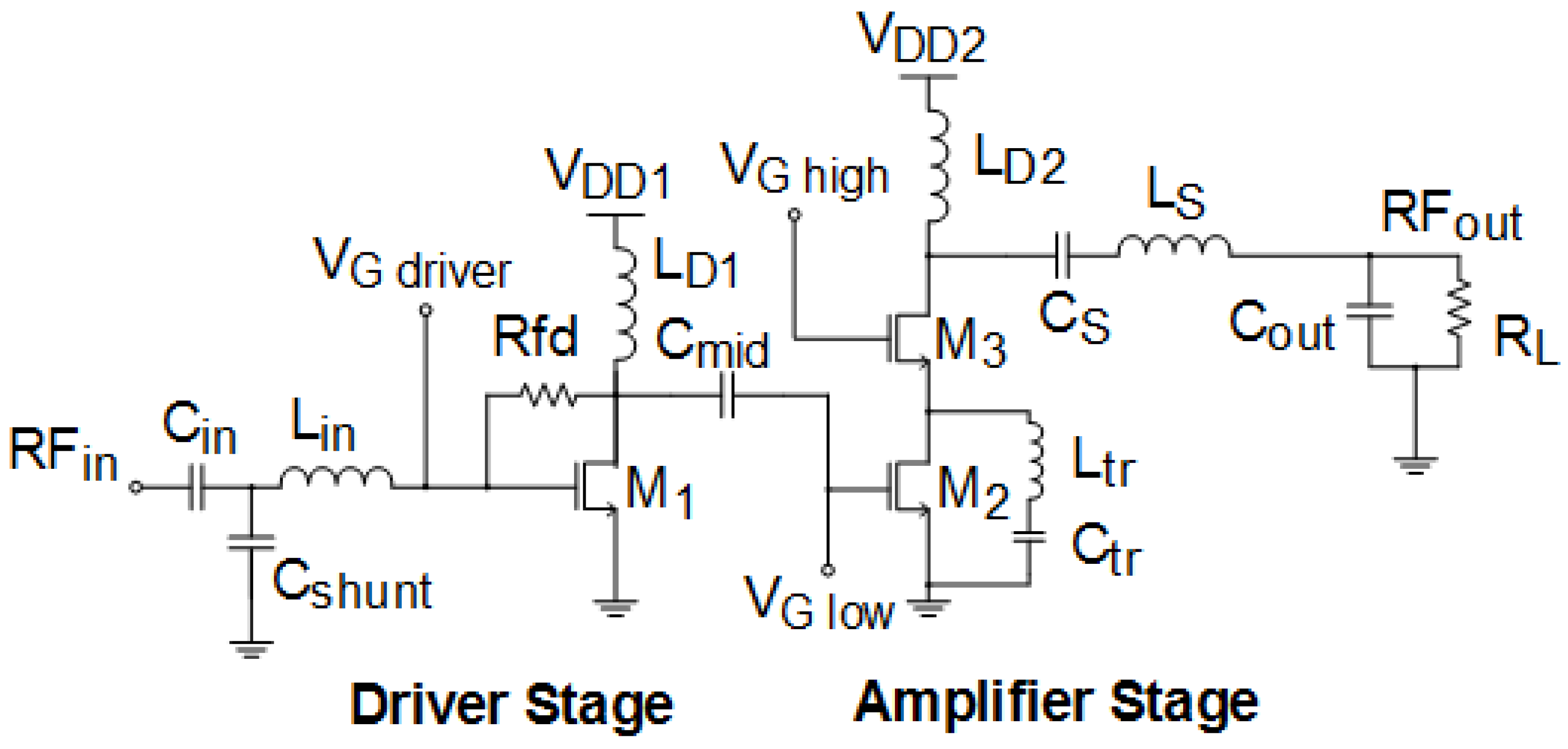
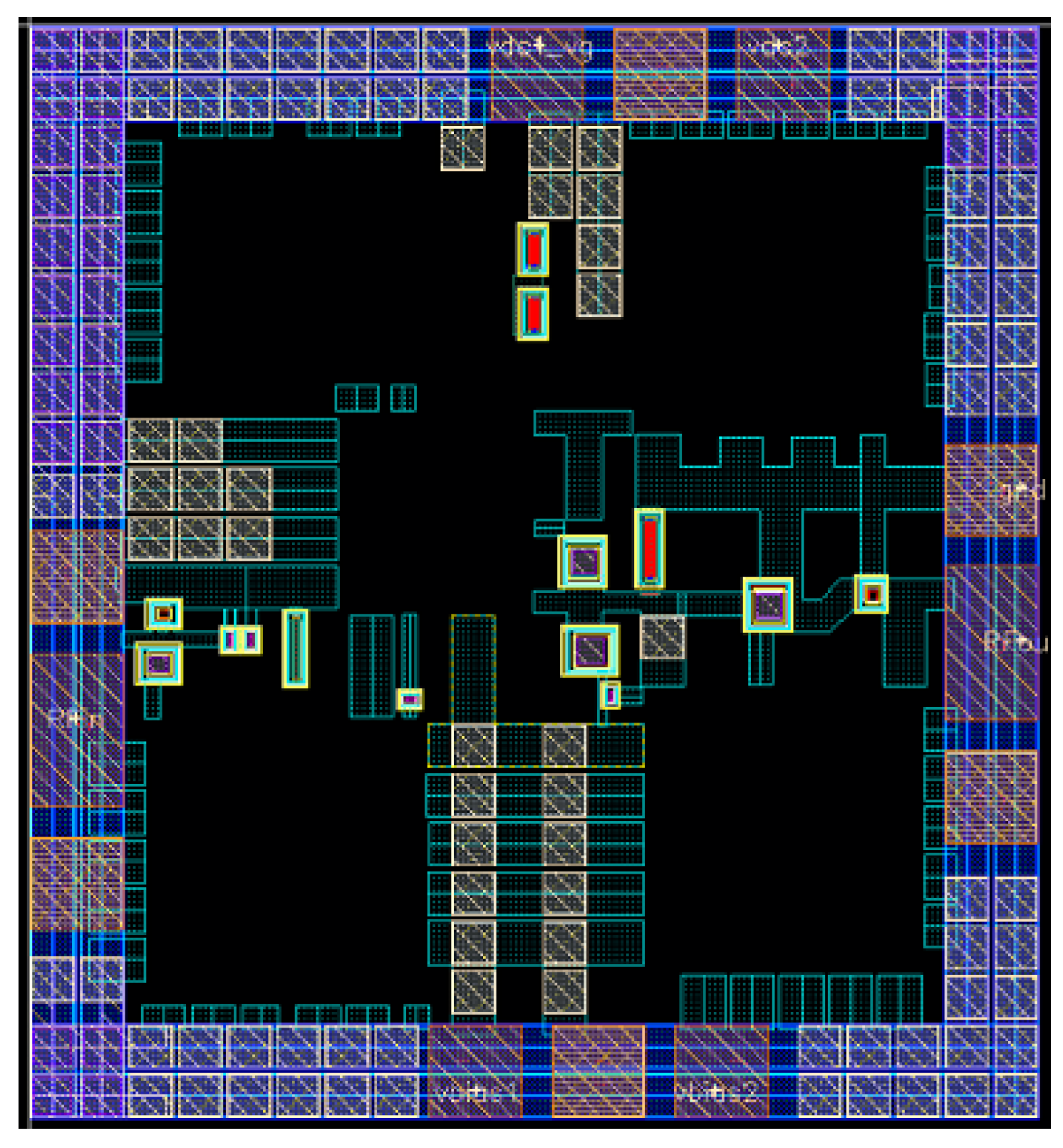
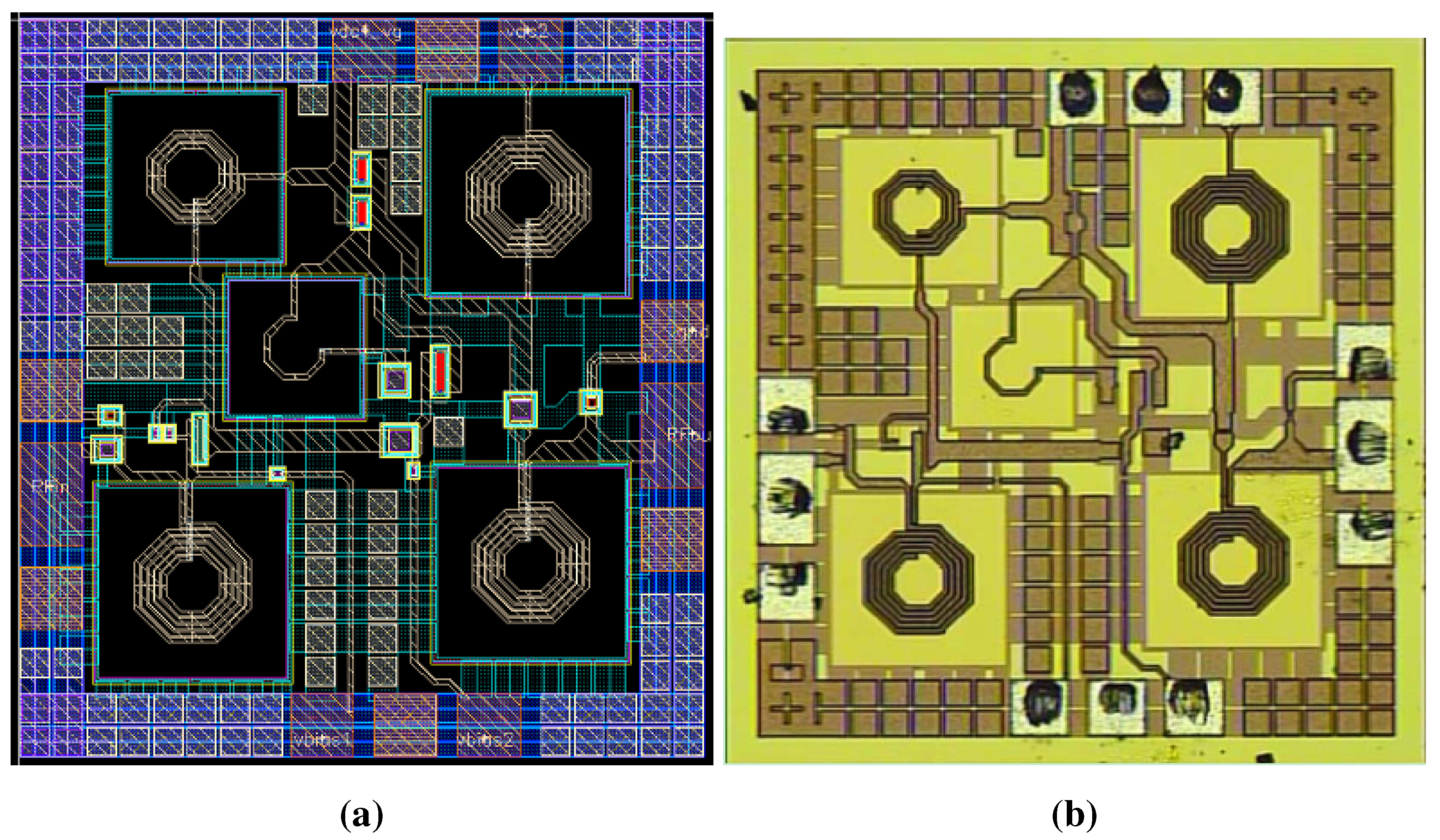
Through a simple Class AB power amplifier, we demonstrate that the split fabrication method is applicable to RF circuit protection and provide a robust, low-cost and highly-secure approach to prevent RF IC piracy. Encouraged by the results from the simple RF circuit, we applied the split manufacturing method and the same security analysis procedure to a Class E power amplifier, which we recently designed, calibrated and fabricated [19]. This Class E power amplifier works at a frequency of 5.2 GHz under 0.18-μm technology and delivers 12.5 dBm output power and 25% power-added efficiency. The circuit consists of five inductors and six capacitors, and the detailed schematic is shown in Figure 11. The layout and the fabricated chip are shown in Figure 12.
Figure 11.
Schematic of a cascode Class E power amplifier.

Figure 12.
(a) Layout of the Class E power amplifier; (b) microchip view of the fabricated Class E power amplifier.
Figure 12.
(a) Layout of the Class E power amplifier; (b) microchip view of the fabricated Class E power amplifier.
The gate bias of each transistor is not the same, nor is the supply voltage to each stage; this significantly increases the effort for attackers with the FEOL to recover the whole circuit, as we will demonstrate shortly. The gate biases for the three transistors are 0.1, 0.7 and 1 V, while the DC supplies are 1 and 2.4 V for the two stages.
5.1. Scenario I: Removal of Metal6 Layers (Inductors)
Figure 13 and Figure 14 show the FEOL part of the power amplifier schematic and its layout after the removal of the metal6 layer. It is clear that the inductors occupy the majority of the RF circuit, which leads the attackers to easily identify that the missing components are inductors. Furthermore, the sample circuit caters to a boosting technique of power-added efficiency (see the loop of , and [19]); therefore, even though only a few interconnections are missing, the attackers may still be unable to recover the circuit topology.
Figure 13.
Schematic of the Class E power amplifier without metal6.
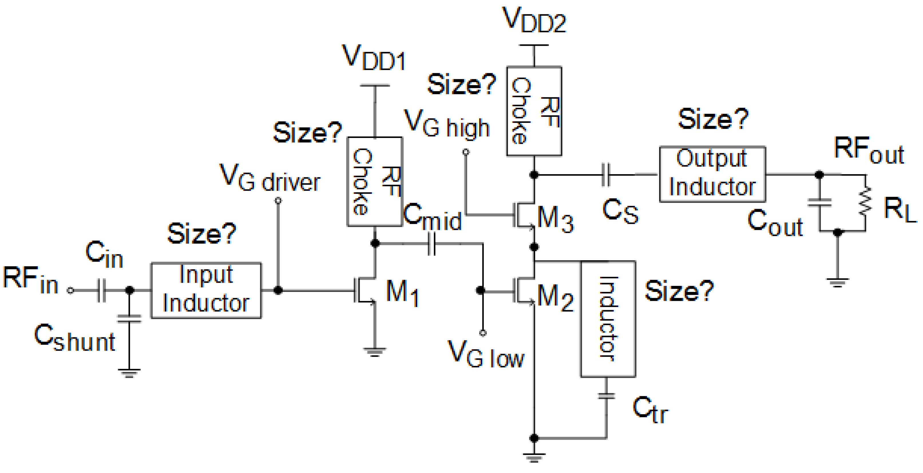
Figure 14.
Layout of the Class E power amplifier without metal6.

In the first stage of the design, there are two inductors, and . In the second stage, there are also two inductors, and . We assume the attacker knows how the inductors are connected. The first task for attackers is to set up the DC biasing and operating frequency. As we can see from the schematic, the DC biasing (gate biasing and supply voltage) is more complicated than that in the one transistor case. The Class E power amplifier has three different gate biases and two different supply voltages. The partial topology may suggest that it is a Class E power amplifier and that the first stage works as a driver (so that a low gate biasing will be used). It can also be interpreted as other types of power amplifiers, as well, such as multi-stage Class A or Class AB power amplifiers, where the much larger gate biasing values are used. Therefore, the attacker needs to sweep the gate biasing by a large range, probably from 0.1–1 V, in order to decide the gate biasing in the first stage. The original design sets the first gate biasing at 0.1 V to make it work as a switch to the power amplifier. For supply voltage, a reasonable range can be from 1–3.3 V in terms of the 0.18-μm technology.
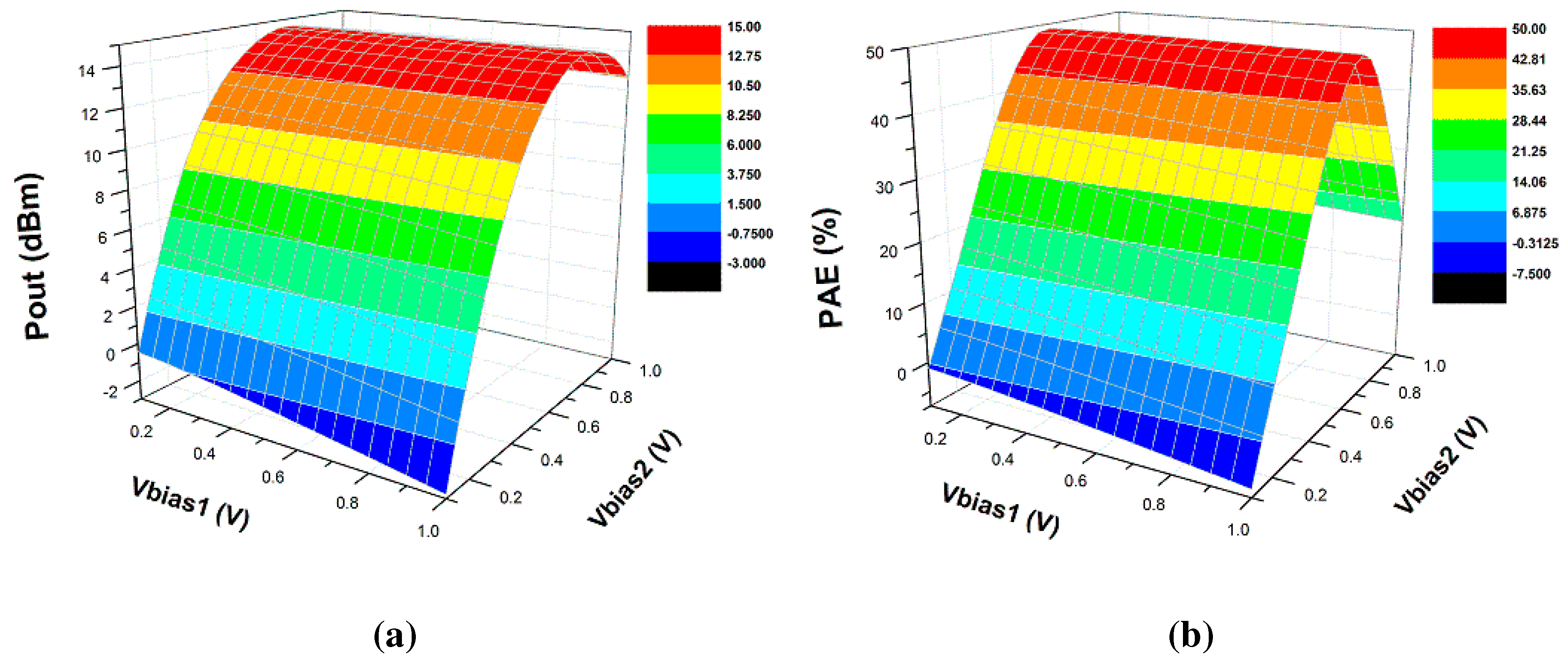
To demonstrate the impact of circuit performance with respect to gate biasing and supply voltage, we add back the correct inductor values and sweep the gate biasing and the supply voltage for both the first and the second stages. The simulation results are shown in Figure 15 and Figure 16. From both figures, we can easily conclude that the overall performance is rather sensitive to the change of the gate biasing and the supply voltage, which makes the selection of operation conditions very important (in the real case that the attackers do not know the inductor values, the task will be further complicated for them to derive the correct operation conditions).
Figure 15.
First-stage and second-stage gate biases versus: (a) output power; (b) power-added efficiency.
Figure 15.
First-stage and second-stage gate biases versus: (a) output power; (b) power-added efficiency.

Normally, a higher supply voltage leads to a better output power, but a high supply voltage will also increase power consumption and decrease power-added efficiency. For this reason, foundries often provide the reference for supply voltage to balance overall performance, i.e., 1.8–3.3 V for the 0.18-μm technology. For example, from Figure 16a, we learn that the output does not change when varies from 1.8–3.3 V; however, the maximum output power occurs when is equal to its highest allowable value. In terms of efficiency shown in Figure 16b, a high power-added efficiency can be achieved when is below 3 V and is around 2 V. With a voltage step of 0.1 V, the attackers have 37 options for selection and 19 options for selection (note that the simulation results are derived from the situation that correct inductors are chosen for demonstrative purposes).
The next step is to derive the inductor values (operating frequency). We assume that the attacker picks the correct DC bias, the gate biases and supply voltages for both stages. The attackers will then sweep the input stage inductor values to test and guess the operating frequency. They may conclude that the operating frequency ranges from 3–7 GHz, indicating that 41 choices are available for a 0.1-GHz step (the actual operating frequency is 5.2 GHz for this design). Once the attackers select the right frequency, they will sweep the inductor values again to check the performance. Although multi-parameter sweeping is applied for all five inductors, to graphically show the simulation procedure, we group the testing cases into three cases. Within each case, only one or two inductors change their values, but the rest of the values are fixed. In the first case, only the input inductor and first stage RF choke vary (see Figure 17); in the second case, the output inductor and the second stage RF choke vary (see Figure 18); in the third case, only varies (see Figure 19).
Figure 16.
First-stage and second-stage supply voltages versus (a) output power; (b) power-added efficiency.
Figure 16.
First-stage and second-stage supply voltages versus (a) output power; (b) power-added efficiency.

Figure 17.
(a) Output power versus and ; (b) power-added efficiency versus and .

Figure 18.
(a) Output power versus Ls and Ld2; (b) power-added efficiency versus Ls and Ld2.
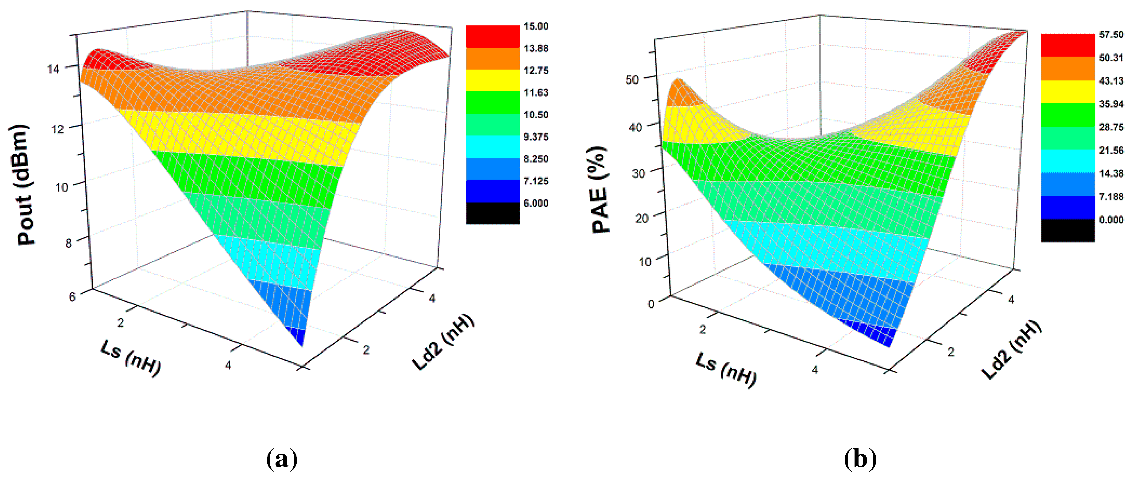
Figure 19.
Overall performance versus.

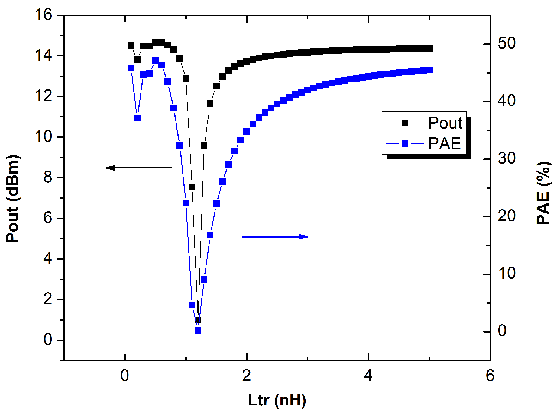
The correct sizes of the input inductor and the first-stage RF choke are 3.61 nH and 1.47 nH, respectively. However, from Figure 17, more than one parameter combination is available to achieve the best performance (note that other inductor values are correctly selected in the simulation). The attackers will have to guess the values of from 2–4 nH and from 1–2 nH purely based on the performance comparison. We want to emphasize that the purpose of applying split manufacturing is to prevent the attackers from learning the exact circuit design that will later be used in critical infrastructures. Through the simulation, attackers may be able to derive an even better performance Class E power amplifier. However, a better design does not mean that it would fit into the overall system design or some application-specific design. For example, the required power amplifier is supposed to have 15 dBm amplification at an operating frequency of 900 MHz. Meanwhile, the attackers retrieve a better amplification of 20 dBm at 2 GHz. In this case, our power amplifier is secured even though attackers come up with a better design. In our Class E power amplifier, the chances that the attacker can derive exactly the same power amplifier are relatively low (4.76% for and 9.09% for given that the rest of the three inductors is correctly selected). To fully elaborate the results, the sweeping range for is from 2–4 nH and for is from 1–2 nH. The sweeping step for both and is 0.1 nH. Thus, the probability to guess right is one out of twenty-one (= 4.76%) and to guess right is one out of eleven (= 9.09%).
The correct size of the output inductor is = 3.61 nH, and the second-stage RF choke is = 4.56 nH. These sizes are within the best performance region, as shown in Figure 18. If the attackers are guided by the performance, they may choose from 3.6–5 nH and from 4–5 nH. Therefore, the probabilities of a correct recovery for the output inductor is 6.25% and for the second-stage RF choke is 9.09%.
The correct size of the inductor is 0.27 nH. This inductor is located in parallel with the transistor M2 and is used for improving the power-added efficiency; however, the inductor is located in the middle of the entire layout, which may be misinterpreted as an intermedium matching network between the first and the second stage. In that case, the attackers have no way to recover the circuit structure; otherwise, as shown in Figure 19, the attackers may select its value from 0.1–0.8 nH with respect to its physical size and the overall circuit performance.
5.2. Scenario II: Removal of Metal5 and Metal6 Layers (Capacitors and Inductors)
In this situation, both metal5 and metal6 are removed from the FEOL. Figure 20 shows the schematic that the untrusted foundry may derive from the FEOL layout. After removing the inductors and capacitors, the interconnections also become an issue. Assuming that the attackers know the amount of capacitors and inductors, as well as the interconnections between transistors and passive components, they will then follow the power amplifier design procedure to achieve the size of all passive components similar to the steps introduced in Section IV-A (Scenario II). Since the circuit is more complicated than the one-transistor power amplifier, the attackers need to follow the power amplifier design procedures stage by stage for this two-stage circuit.
Figure 20.
Schematic of the Class E power amplifier with metal5 and metal6 removed (no inductors and capacitors).
Figure 20.
Schematic of the Class E power amplifier with metal5 and metal6 removed (no inductors and capacitors).

The First Stage:The procedure to derive the DC biasing and operating frequency for the first stage is similar to that in Scenario I and is omitted here. We assume that the attackers already know the DC biasing and operating frequency. After deriving the DC biasing, the attackers should know that the first stage works as a driver in a Class E power amplifier; then, they will run the source pull simulation to rebuild the input matching network. The attackers with RF experience may correctly guess that one inductor and two capacitors are in the matching network; therefore, they may only select the network topology with three components when running the source pull simulation. Figure 21 details the two possible input matching networks. The attackers will then sweep the RF choke to compare the performance as shown in Figure 22. The simulation result will guide the attackers to decide the first-stage RF choke inductor to be from 1–2 nH.
Figure 21.
Two possible input matching networks.

Figure 22.
Output performance versus first-stage RF choke .

The Second Stage:Again, we assume that the attackers know the DC biasing of the second stage and that they know that the second stage is of a cascode topology. Before the attackers can run the load pull simulation, they need to randomly select the second-stage RF choke and the coupling capacitor . Considering the fact that reasonable ranges for both components are from 1–5 nH for the inductor and from 0.1–3 pF for the capacitor, the attackers have to run different load pull simulations. Since there is only one inductor and one capacitor in the output matching network, two topologies may be selected, which are shown in Figure 23.
Figure 23.
Two possible output matching networks.

After the previous work, there are still two components unknown to the attackers, the inductor and the capacitor . As we mentioned earlier, these two components are interpreted as an intermediate matching network. Only very experienced RF designers would think about the other possibility, i.e., the extra components are used to improve the power-added efficiency. Only if the attackers know the functionality of the two passive components can they sweep the component values to get the same results as those in Figure 19.
5.3. Scenario III: Obfuscation Techniques
In the Class E power amplifier, the proposed obfuscation techniques, both the enlarged passive component area and the extra empty blocks, will further help defend the circuit from IP piracy.
First, the area of the inductor block increases proportionally to the value of the inductor. If the designers enlarge the inductor block area, the attackers may derive the inductor values in a wrong range. Since the expanded inductor blocks are the only design overhead, the performance impact can be minimized while the security level using split manufacturing will be improved significantly. This obfuscation approach, however, does not add obstacles to attackers in routing recovery, since the topology remains the same after the circuit is obfuscated.
Second, the designer can insert more empty blocks in the layout, although the dummy blocks may increase performance overhead. A proper co-design can help alleviate the issue if the designers consider security in the early stages. The inserted dummy blocks can upgrade the security level of the circuit under protection. Assuming that two dummy blocks are added in the input (or output) matching network, the additional blocks can completely mislead the attackers to a wrong design topology and interconnections when the attackers perform the load simulation. Therefore, after applying the second obfuscation method, the topology correctness becomes another level of protection preventing attackers from learning the circuit structure.
6. Discussion
The main focus of our paper is split manufacturing on radio-frequency design. We have presented a small portion of the obfuscation technique. However, we believe that the concrete study of the obfuscation technique can further improve the security of split manufacturing. For instance, the original design could deliberately include many sub-optimal components along with many optimally-designed components. Then, the attacker is faced with a dilemma of whether any given local component is intended to be realized with the optimal parameters or not. Deliberately creating this dilemma for each component could perhaps make the overall design even harder to retrieve.
7. Conclusions
Split manufacturing has presented a new solution against reverse engineering and IP piracy as the IC design flow becomes more globalized. Different from all previous work to apply the split manufacturing in digital circuits, we introduced the first attempt to implement a similar method in RF designs. Quantitative analysis was presented to assess the security protection level for RF designs in the event that untrusted foundries would like to recover the circuit designs based on part of the circuit layout. To further guide the application of split manufacturing in RF circuits, three different FEOL and BEOL separation and obfuscation methods were introduced. All of these methods were demonstrated on two RF circuits: a simple Class AB power amplifier and a more sophisticated Class E power amplifier. The experimental results confirmed that the unknown passive components, either inductors or capacitors, along with the missing DC biasing conditions, can raise a significant amount of uncertainty for the attacker to recover the RF circuits. In conclusion, split manufacturing is more effective in RF IC trust than in digital circuit security. We hope to pursue a real silicon-level implementation in our future work.
Author Contributions
Y. Bi performed the experimental results and wrote the first version paper. J.S.Yuan guided the research and reviewed the paper. Y. Jin guided the research and edited the final version of the paper. All authors read and approved the final paper.
Conflicts of Interest
The authors declare no conflict of interest.
References
- Defense Science Board (DSB) study on High Performance Microchip Supply. Available online: http://www.cra.org/govaffairs/images/2005-02-HPMS_Report_Final.pdf (accessed on 15 August 2005).
- Adee, S. The Hunt For The Kill Switch. IEEE Spectr. 2008, 45, 34–39. [Google Scholar] [CrossRef]
- Yeh, A. Trends in the Global IC Design Service Market; DIGITIMES Research: Taipei, Taiwan, 2007. [Google Scholar]
- Jin, Y.; Yang, B.; Makris, Y. Cycle-accurate information assurance by proof-carrying based signal sensitivity tracing. In Proceedings of the IEEE International Symposium on Hardware-Oriented Security and Trust (HOST), Austin, TX, USA, 2–3 June 2013; pp. 99–106.
- Tehranipoor, M.; Koushanfar, F. A Survey of Hardware Trojan Taxonomy and Detection. IEEE Des. Test Comput. 2010, 27, 10–25. [Google Scholar] [CrossRef]
- Bi, Y.; Gaillardon, P.-E.; Hu, X.; Niemier, M.; Yuan, J.-S.; Jin, Y. Leveraging Emerging Technology for Hardware Security—Case Study on Silicon Nanowire FETs and Graphene SymFETs. In Proceedings of the 2014 IEEE 23rd Asian Test Symposium (ATS), Hangzhou, China, 16–19 November 2014; pp. 342–347.
- Intelligence Advanced Research Projects Activity. Trusted Integrated Chips (TIC) Program. Available online: https://www.fbo.gov/notices/36a51487427786930733999edc40f321 (accessed on 15 August 2011).
- Rajendran, J.; Sinanoglu, O.; Karri, R. Is split manufacturing secure? In Proceedings of the Design, Automation Test in Europe Conference Exhibition (DATE), Grenoble, France, 18–22 March 2013; pp. 1259–1264.
- Imeson, F.; Emtenan, A.; Garg, S.; Tripunitara, M. Securing Computer Hardware Using 3D Integrated Circuit (IC) Technology and Split Manufacturing for Obfuscation. In Proceedings of the 22nd USENIX Security Symposium, Washington, DC, USA, 14–16 August 2013; pp. 495–510.
- Hill, B.; Karmazin, R.; Otero, C.T.O.; Tse, J.; Manohar, R. A split-foundry asynchronous FPGA. In Proceedings of the Custom Integrated Circuits Conference (CICC), San Jose, CA, USA, 22–25 September 2013; pp. 1–4.
- Vaidyanathan, K.; Das, B.P.; Sumbul, E.; Liu, R.; Pileggi, L. Building Trusted ICs using Split Fabrication. In Proceedings of the 2014 IEEE International Symposium on Hardware-Oriented Security and Trust (HOST), Arlington, VA, USA, 6–7 May 2014.
- Vaidyanathan, K.; Liu, R.; Sumbul, E.; Zhu, Q.; Franchetti, F.; Pileggi, L. Efficient and Secure Intellectual Property (IP) Design with Split Fabrication. In Proceedings of the 2014 IEEE International Symposium on Hardware-Oriented Security and Trust (HOST), Arlington, VA, USA, 6–7 May 2014.
- Jagasivamani, M.; Gadfort, P.; Sika, M.; Bajura, M.; Fritze, M. Split-Fabrication Obfuscation: Metrics and Techniques. In Proceedings of the 2014 IEEE International Symposium on Hardware-Oriented Security and Trust (HOST), Arlington, VA, USA, 6–7 May 2014.
- Vaidyanathan, K.; Das, B.P.; Pileggi, L. Detecting Reliability Attacks During Split Fabrication Using Test-only BEOL Stack. In Proceedings of the 51st Annual Design Automation Conference on Design Automation Conference, San Francisco, CA, USA, 1–5 June 2014; pp. 156–161.
- Bi, Y.; Yuan, J.S.; Jin, Y. Split Manufacturing in Radio-Frequency Designs. In Proceedings of the International Conference on Security and Management (SAM), Las Vegas, NV, USA, 27–30 July 2015; pp. 204–210.
- Yuan, J.S.; Xu, Y.; Yen, S.D.; Bi, Y.; Hwang, G.W. Hot Carrier Injection Stress Effect on a 65 nm LNA at 70 GHz. IEEE Trans. Device Mater. Reliab. 2014, 14, 931–934. [Google Scholar] [CrossRef]
- Yuan, J.S.; Bi, Y. Process and temperature robust voltage multiplier design for RF energy harvesting. Microelectron. Reliab. 2015, 55, 107–113. [Google Scholar] [CrossRef]
- Carls, J.; Eickhoff, R.; Sakalas, P.; von der Mark, S.; Wehrli, S. Design of a C-Band CMOS class AB power amplifier for an ultra low supply voltage of 1.9 V. In Proceedings of the SBMO/IEEE MTT-S International Microwave and Optoelectronics Conference, Brazil, 29 October–1 November 2007; pp. 786–789.
- Yuan, J.-S.; Yen, H.D.; Chen, S.; Wang, R.L.; Huang, G.W.; Juang, Y.Z.; Tu, C.H.; Yeh, W.K.; Ma, J. Experimental Verification of RF Stress Effect on Cascode Class-E PA Performance and Reliability. IEEE Trans. Device Mater. Reliab. 2012, 12, 369–375. [Google Scholar] [CrossRef]
© 2015 by the authors; licensee MDPI, Basel, Switzerland. This article is an open access article distributed under the terms and conditions of the Creative Commons Attribution license (http://creativecommons.org/licenses/by/4.0/).
Share and Cite
MDPI and ACS Style
Bi, Y.; Yuan, J.S.; Jin, Y. Beyond the Interconnections: Split Manufacturing in RF Designs. Electronics 2015, 4, 541-564. https://doi.org/10.3390/electronics4030541
AMA Style
Bi Y, Yuan JS, Jin Y. Beyond the Interconnections: Split Manufacturing in RF Designs. Electronics. 2015; 4(3):541-564. https://doi.org/10.3390/electronics4030541
Chicago/Turabian StyleBi, Yu, Jiann S. Yuan, and Yier Jin. 2015. "Beyond the Interconnections: Split Manufacturing in RF Designs" Electronics 4, no. 3: 541-564. https://doi.org/10.3390/electronics4030541