
A 0.8–8 GHz Multi-Section Coupled Line Balun

EECS Department, The University of Toledo, 2801 W Bancroft St., Toledo, OH 43606, USA
*
Author to whom correspondence should be addressed.
†
These authors contributed equally to this work.
Electronics 2015, 4(2), 274-282; https://doi.org/10.3390/electronics4020274
Submission received: 19 March 2015
/
Revised: 18 April 2015
/
Accepted: 24 April 2015
/
Published: 30 April 2015
(This article belongs to the Special Issue Microwave/ Millimeter-Wave Devices and MMICs)
Abstract
:In this work, we propose a wideband multi-section transforming coupled-line balun using near equal length transmission line elements. The resulting design is realized by cascading several coupled-lines with minimal discontinuities. The multi-section Chebyshev matching optimizes bandwidth at the expense of passband ripple. The proposed design delivers good impedance matching and consistent 180° phase shift over 0.8–8 GHz frequency spectrum. Furthermore, the need for vias in conventional balun designs is relaxed by replacing the short-circuited (SC) terminal by its equivalent dual open-circuited (OC) element. The proposed design is simulated, fabricated, and measured. Both simulated and measured results are in a good agreement, and show an input port matching of below −9.7 dB over the design bandwidth, with a maximum phase and amplitude imbalance of 2.1° and 0.9 dB, respectively.
1. Introduction
Baluns are class of passive microwave components used to transform transmission line mode from balanced to unbalanced and vice versa by providing the required impedance transformation as the balanced and unbalanced port impedances are usually unmatched. Given the important role of baluns in many classical and modern applications [1], such as common mode rejection in balanced architectures, push-pull amplifiers and double balanced mixers, broadening a balun operational bandwidth is still an ongoing research topic. In this context, scholars worldwide reported several wideband balun designs in support of the emerging broadband technologies and multiband integrated systems.
To this end, Marchand, multi-section coupled-lines, composite right/left handed transmission lines, and CPW baluns have been recently introduced. In [2], wideband compensated and uncompensated Marchand baluns were proposed using step transformers. However, the vias accompanying the design increases its structural complexity, sensitivity, and fabrication cost. Multi section coupled-line baluns were realized in [3] using two-line edge coupled microstrips. Hence, simplifying the complexity order by eliminating the vias was obtained at the expense of the operating bandwidth. Lim et al. proposed a wideband CPW balun with the aid of a multistage out-of-phase Wilkinson power divider (WPD) [4], which is although interesting is limited to the number of consecutive stages in the WPD that may degrade the overall electrical performance due to the resulting crossovers. Fractal shape composite right/left handed transmission line broadband balun [5] was designed. Such a technique resulted in a compact design, but the added complexity may introduce ports overlapping if proper care is not taken during simulations. Another planar balun was designed on a single layer substrate in [6]; however, the relatively narrow bandwidth was a major drawback. Furthermore, a multi-layered wideband balun [7] in the C- and X-band with a number of holes was designed making the design highly complex. A wideband balun using parallel strips was designed in [8], which is synthesized using a third order Chebyshev response. The design has a symmetrical four-port structure incorporating vias with relatively moderate operating bandwidth. Microstrip to slotline transitions was discussed in [9], where the balun implemented was compact in size covering ultrawide bandwidth. The disadvantage of the design though was the use of high dielectric constant (ɛr > 10) material in order to match the slotline transition to 50 Ω microstrip line. Additionally, high radiation loss is associated with such transitions.
In this work, we propose a broadband three-port coupled-line balun derived from a four-port symmetrical network. The proposed balun covers the frequency spectrum of 0.8–8 GHz by the virtue of utilizing tightly coupled tapered lines that have the benefit of being straightforwardly handled, compact, and exhibits broad frequency spectrum with applications in WiMAX, WLAN, Bluetooth and ISM bands.
2. Coupled Line Balun Theory
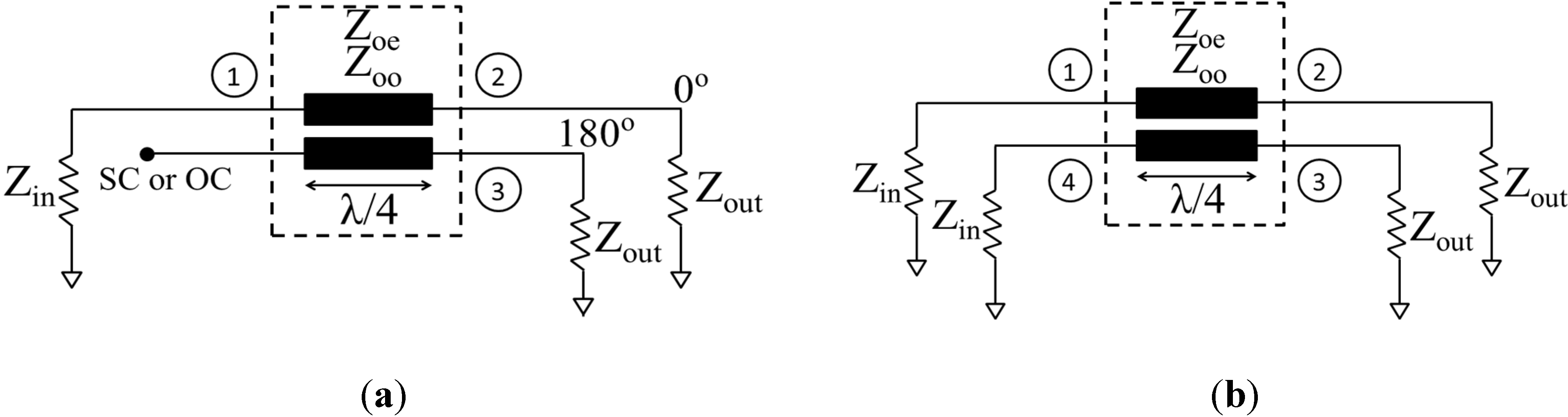
This section briefly describes the general theory of utilizing a symmetric four-port network to implement a three-port coupled line baluns. First, the coupled line ABCD parameters are derived in terms of even and odd modes as in (1),
where V is the voltage, I is the current, Zc is the characteristic impedance, θ is the electrical length the subscripts o, e correspond to the odd and even modes, respectively, and the superscripts 1, 2, 3 correspond to the physical port number, while 4 correspond to the open-circuit port as depicted in Figure 1 [10]. Figure 1a shows the diagram of a typical quarter-wave coupled-line balun capable of providing balanced outputs to load terminations (Zout) from unbalanced input impedance (Zin). The quarter-wavelength corresponds to the center frequency of operation and one of the coupled-line terminals is terminated to ensure full reflection. Thus, the combined four-port S-matrix obtained from (1) is reduced to a three-port matrix by assigning boundaries at the reflecting port of the four-port network shown in Figure 1b. The three-port S-parameters characterizing the balun operation is then given by (2):
S11 = 0, and S21 = −S31
The required coupled-line odd- and even-mode impedances can be derived from the corresponding four-port network shown in Figure 1b. The short- or open-circuited (SC or OC) terminal is replaced by a load Zin to form a symmetrical network enabling the decomposition of odd- and even-mode circuits. To satisfy (2), conditions necessary for synthesizing three-port balun are given by (3) and (4):
where, Γ represents the total reflectance coefficient, Γe and Γo are the even- and odd-mode reflectance coefficients, respectively. Equation (3) is satisfied for Γ = 1, Γe = −1 and Γo = 0.33 and Equation (4) is satisfied for Γ = −1, Γe = 1 and Γo = −0.33. Hence, the even-mode reflection coefficients (Γe) must equal to +1 and −1, whereas the odd-mode reflection coefficients (Γo) equal to −0.33 and 0.33 for the SC and OC cases, respectively [11]. Consequently, even- and odd-mode impedances of the SC and OC cases can be defined as in Equations (5) and (6):
As indicated in Equations (5) and (6), a balun function can be achieved if the four-port symmetrical network operates as a bandstop network in the even-mode and as an impedance transformer in the odd-mode. The realization of ideal OC or SC in the even mode is challenging, thus approximation to very high or very low even-mode impedances are required although this may degrade the balun amplitude balance.
Figure 1.
Quarter-wave coupled-line: (a) balun network; and (b) its corresponding four-port network for odd- and even-mode analysis.
Figure 1.
Quarter-wave coupled-line: (a) balun network; and (b) its corresponding four-port network for odd- and even-mode analysis.

3. Design Explanation
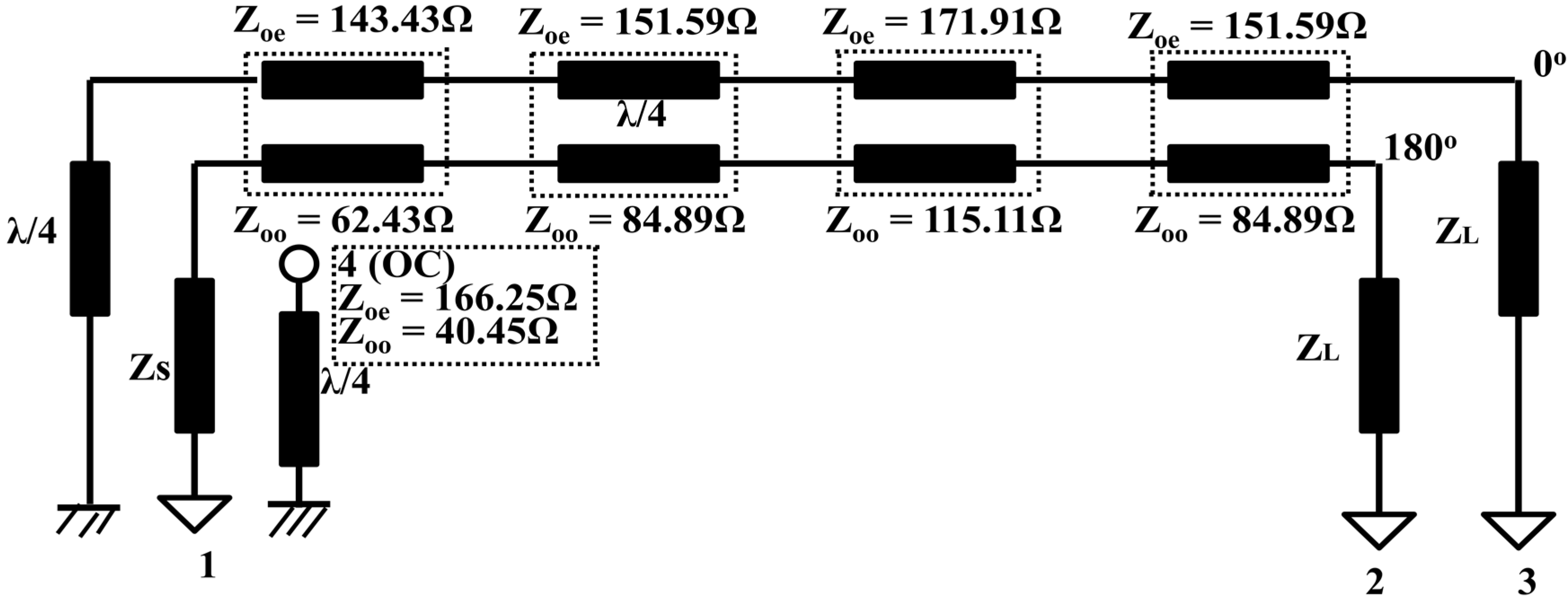
For most coupled-line structures in the literature, Zoe is greater than Zoo. Hence, the short-circuited case with tightly coupled microstrip line is employed to achieve the required high Zoe and specific Zoo. In this work, we will consider the case where port 4 is open circuited and propose to use a very low even-mode impedances for our design (i.e., open circuited in even-mode), so that Zoe < Zoo, hence via to ground is not required. This can be established by introducing coupling arms l1 and l5 as depicted in the proposed configuration of Figure 2 (at port 1) to provide the necessary equivalent OC for the four-port network in the even-mode analysis. Furthermore, stepped impedance tightly coupled lines provide the necessary broad bandwidth for the proposed design.
Figure 2.
Schematic of the proposed wideband multi-section coupled-line balun.

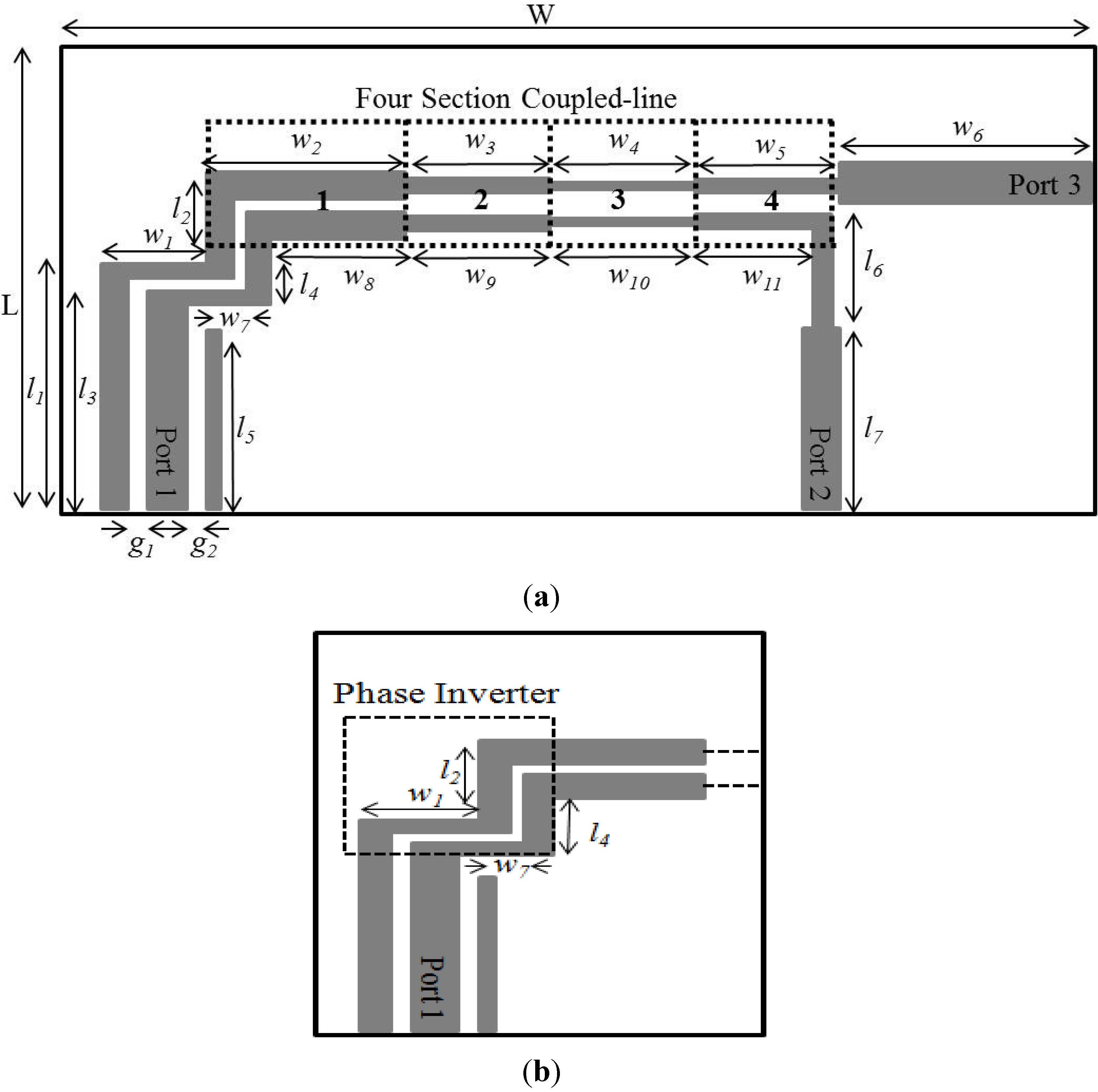
Figure 3a shows the physical layout of the proposed balun along with its dimensions (in millimeters). All three ports are matched to 50-Ω impedance. By properly optimizing the lengths and widths of the stepped elements, the phase can be kept constant over a broad bandwidth (i.e., 180° phase difference between the balanced ports 2 and 3). Lengths w1+ l2 and w7+ l4 realize the phase inverter function. The λ/4 lengths provide the required 180° phase shift between port 2 and 3. Figure 3b represents the phase inverter block in the proposed balun design. The coupled lines w2 and w8, w3 and w9, w4 and w10, w5 and w11 constitute the four-section coupled line configuration. The parallel tapered lines are tightly coupled with a smallest separation distance equals to 0.4 mm. Arms l1 and l5 provide additional coupling between the coupled lines by suppressing the even mode impedance near port 1, while l6 provides impedance matching for port 3.
Four stepped coupled lines were optimized using a full-wave electromagnetic simulator and found to be sufficient to achieve the design bandwidth from 0.8 to 8 GHz. The design is carried out on a FR4 substrate with a relative permittivity and thickness of 4.2 and 1.5 mm, respectively. Optimal impedance values are listed in Table 1.

| Section 1 | Section 2 | Section 3 | Section 4 | OC | |
|---|---|---|---|---|---|
| Zoe (Ω) | 142.43 | 151.59 | 171.91 | 151.59 | 166.25 |
| Zoo (Ω) | 62.43 | 84.89 | 115.11 | 84.89 | 40.45 |
| Metal width (mm) | 0.6 | 0.4 | 0.2 | 0.4 | 0.5 |
| Trace spacing (mm) | 0.4 | 0.8 | 1.2 | 0.8 | 0.05 |
Figure 3.
(a) Layout of the proposed balun in mm. (w1 = 10.2, w2 = 9.7, w3 = 12.9, w4 = 12.8, w5 = 18.6, w6 = 15, w7 = 10, w8 = 8.4, w9 = 12.9, w10 = 12.8, w11 = 13, g1 = g2 = 0.1, l1 = 16.8, l2 = 6.8, l3 = 16, l4 = 7, l5 = 14, l6 = 8, l7 = 14.7); (b). w1 + l2 and w7 + l4 together perform the phase shifting mechanism.

4. Results and Discussion
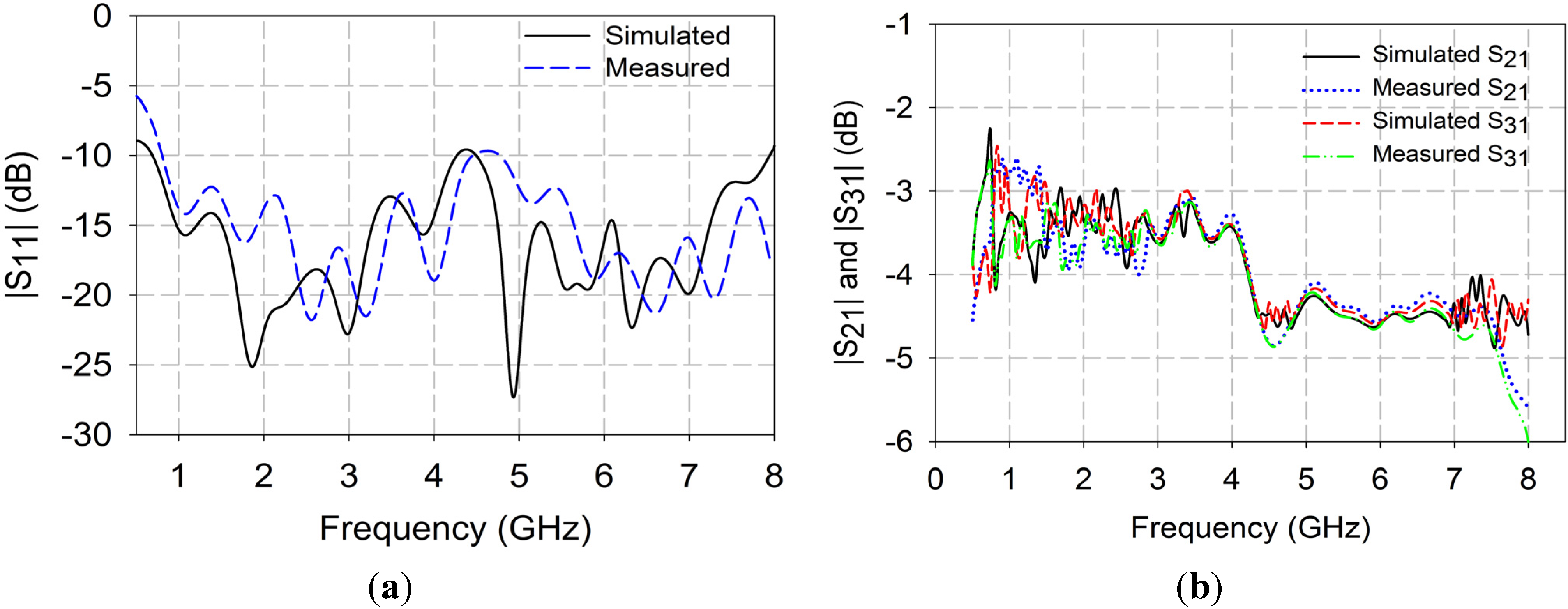
Figure 4 represents the simulated and measured S-parameters of the proposed design that is modeled in Ansys-HFSS [12] and tested after a three-port calibration to a Rhode and Schwarz ZVB20 vector network analyzer. Each stepped line contributes in a resonant frequency, which results in enhancing the matching due to the constant input impedance stepped lines offer for a wide frequency range. A broadband performance is observed in the input port matching parameter (S11), which is less than −9.7 dB over the 0.8–8 GHz frequency range (Figure 4a). The transmission parameters (S21 and S31) are around −4 dB in average over the design bandwidth (Figure 4b).
Figure 4.
Simulated and measured S-parameters of the proposed balun: (a) |S11|; and (b) |S21| and |S31|.
Figure 4.
Simulated and measured S-parameters of the proposed balun: (a) |S11|; and (b) |S21| and |S31|.

Due to the length of the additional coupling line (l5), the insertion loss tends to increase over higher frequencies. The small discrepancies between the simulated and measured results are thought to be from the fabrication/measurement tolerances. The results of the proposed balun are compared with other published works and summarized in Table 2.
| Reference | Absolute Bandwidth (GHz) | Vias | Complexity | Area (in terms of λ2) |
|---|---|---|---|---|
| [2] | 1–7.5 | Yes | Many vias make design complex | 0.61 × 1.17 |
| [3] | 0.5–3.5 | No | Modified ground plane | 0.44 × 1.02 |
| [4] | 0.8–3.2 | No | Intercrossing after each stage | 0.44 × 1.17 |
| [5] | 1–2.25 | No | Fractal geometry | 0.42 × 0.44 |
| [6] | 1.7–3.3 | Yes | Less complex | 0.58 × 1.02 |
| [7] | 6.11–13.83 | Yes | Multi-layered | 0.48 × 0.76 |
| [8] | 0.72–2.05 | Yes | Less complex | 0.90 × 1.04 |
| This work | 0.8–8 | No | Less complex | 0.36 × 1.00 |
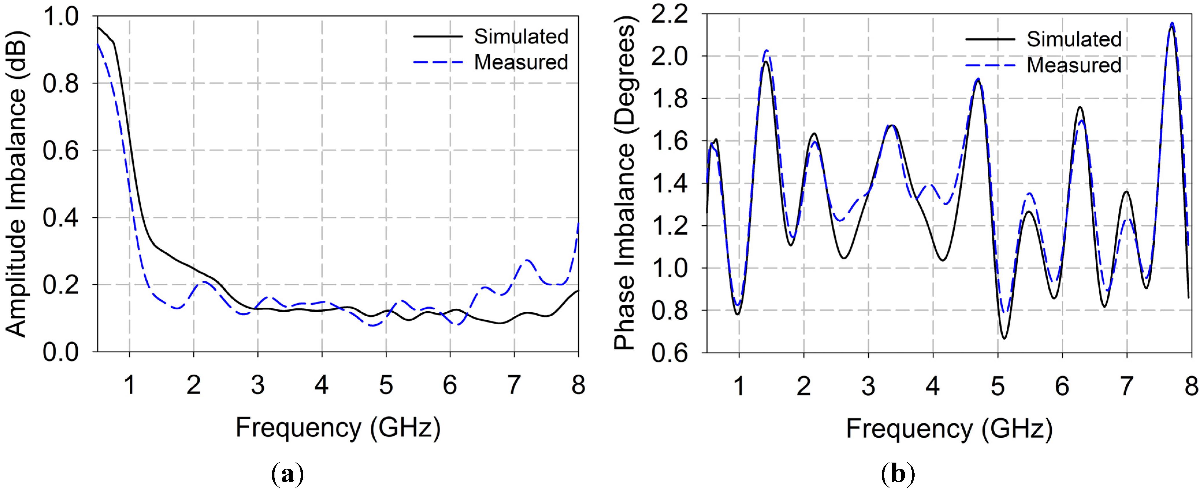
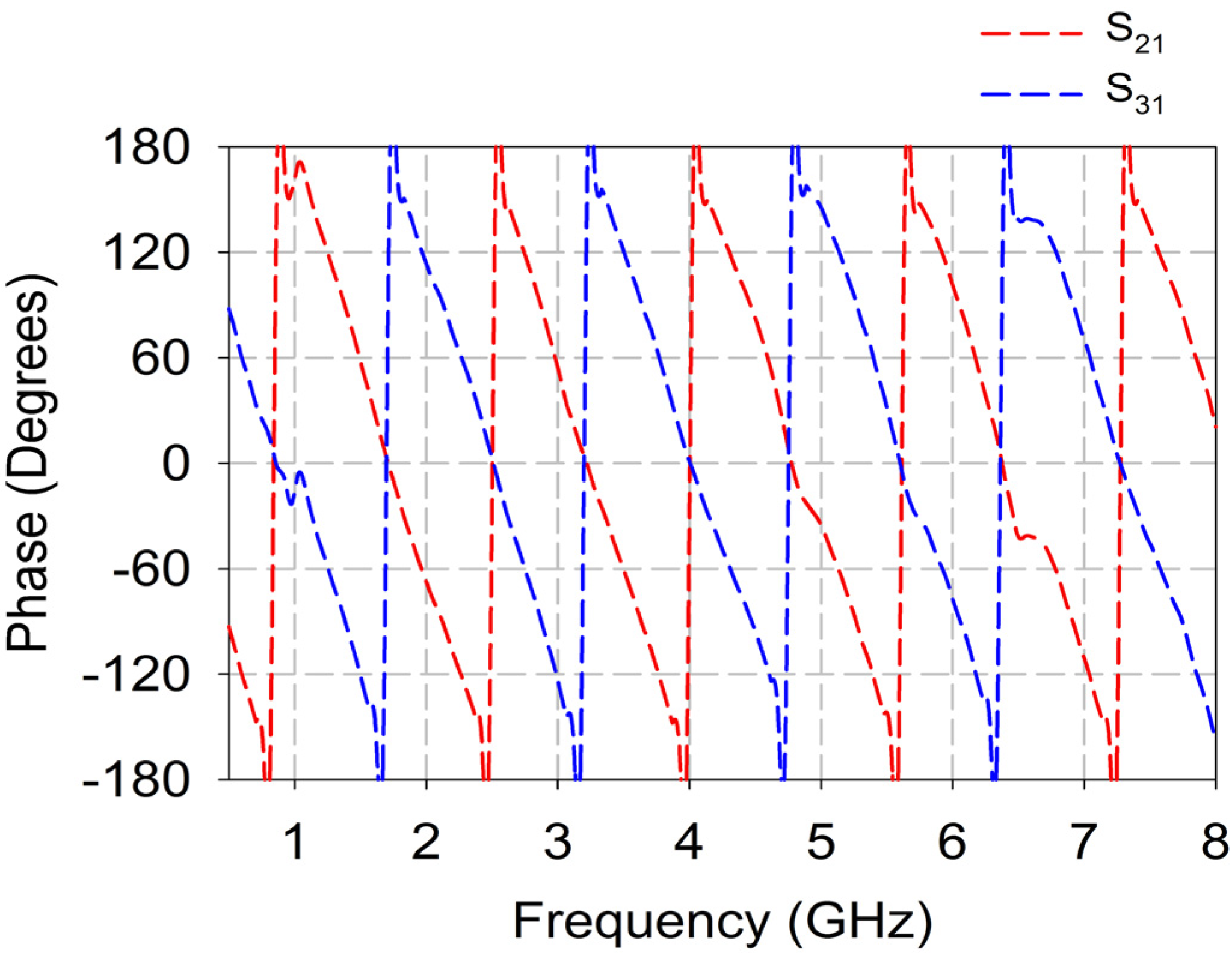
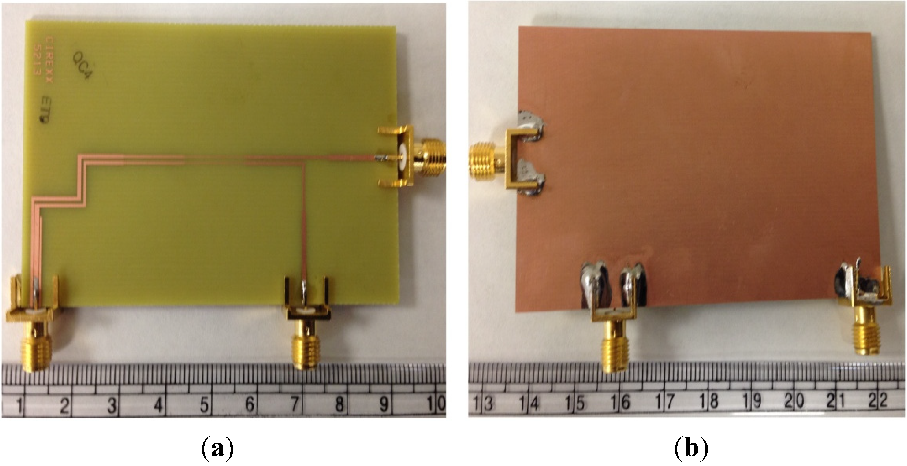
Figure 5 depicts the amplitude and phase imbalance defined by |S21|–|S31| and ∠S21–∠S31–180°, respectively, of the proposed balun. As can be noticed from Figure 5a, the maximum amplitude imbalance is around 0.9 dB at 0.8 GHz. On the other hand, the average phase imbalance, shown in Figure 5b, is observed to be around 1.4° across the 0.8–8 GHz band, while Figure 6 shows the measured phase response of the proposed balun at port 2 and port 3. Figure 7 shows a photograph of the fabricated prototype.
Figure 5.
Simulated and measured imbalance: (a) magnitude; and (b) phase.

Figure 6.
Measured phase response of the proposed balun at port 2 and port 3.

Figure 7.
Photograph of the fabricated broadband balun: (a) top view; and (b) bottom view.

5. Conclusions
A broadband coupled-line balun functional in the 0.8–8 GHz frequency range has been proposed. The design is a three-port coupled-line microstrip balun derived from a symmetrical four-port network with broadband matching obtained using stepped and tightly coupled lines. The measured results indicate an average amplitude imbalance of 0.2 dB and phase imbalance of 1.4°. The proposed balun is advantageous in being straightforwardly handled, compact, and exhibits a broad frequency spectrum.
Acknowledgments
This work was supported by the NSF EARS Award # 1247946.
Author Contributions
S. Itapu, M. Almalkawi and V. Devabhaktuni developed the theory and wrote the paper.
Conflicts of Interest
The authors declare no conflict of interest.
References
- Sturdivant, R. Balun designs for wireless, mixers, amplifiers and antennas. Appl. Microwaves 1993, 5, 34–44. [Google Scholar]
- Xu, Z.; MacEachern, L. Optimum design of wideband compensated and uncompensated Marchand Baluns with step transformers. IEEE Trans. Microw. Theory Tech. 2009, 57, 2064–2071. [Google Scholar] [CrossRef]
- Ang, K.S.; Leong, Y.C.; Lee, C.H. Multisection impedance-transforming coupled-line baluns. IEEE Trans. Microw. Theory Tech. 2003, 51, 536–541. [Google Scholar] [CrossRef]
- Lim, J.S.; Park, U.H.; Koo, J.J.; Jeong, Y.C.; Ahn, D. A 800- to 3200-MHz wideband CPW balun using multistage Wilkinson structure. In Proceedings of IEEE MTT-S International Microwave Symposium Digest, San Francisco, CA, USA, 11–16 June 2006; pp. 1141–1144.
- Xu, H.X.; Wang, G.M.; Chen, X.; Li, T.P. Broadband balun using fully artificial fractal shaped composite right/left handed transmission line. IEEE Microw. Wireless Compon. Lett. 2012, 22, 16–18. [Google Scholar] [CrossRef]
- Zhang, Z.Y.; Guo, Y.G.; Ong, L.C.; Chia, M.Y.W. A new wide-band planar balun on a single-layer PCB. IEEE Microw. Wireless Compon. Lett. 2005, 15, 416–418. [Google Scholar] [CrossRef]
- Peng, W.; Quan, X. A wideband microstrip balun structure. In Proceedings of IEEE MTT-S International Microwave Symposium (IMS), Tampa, FL, USA, 1–6 June 2014; pp. 1–3.
- Jin, S.; Rongguo, Z.; Chang, C.; Hyoungsoo, K.; Hualiang, Z. Design of a wideband balun using parallel strips. IEEE Microw. Wireless Compon. Lett. 2013, 23, 125–127. [Google Scholar] [CrossRef]
- Nguyen, P.T.; Abbosh, A.; Crozier, S. Wideband and compact quasi-Yagi antenna intergrated with balun of microstrip to slotline transitions. Electron. Lett. 2013, 49, 88–89. [Google Scholar] [CrossRef]
- Mongia, R.K.; Bahl, I.J.; Bhartia, P.; Hong, J. RF and Microwave Coupled-line Circuits, 2nd ed.; Artech Publications: Norwood, MA, USA, 2007. [Google Scholar]
- Leong, Y.C.; Ang, K.S.; Lee, C.H. A derivation of a class of 3-port baluns from symmetrical 4-port networks. In Proceedings of IEEE MTT-S International Microwave Symposium Digest, Seattle, WA, USA, 2–7 June 2002; pp. 1165–1168.
- ANSYS-High Frequency Structure Simulator (HFSS); Ansys. Inc.: Canonsburg, PA, USA, 2011.
© 2015 by the authors; licensee MDPI, Basel, Switzerland. This article is an open access article distributed under the terms and conditions of the Creative Commons Attribution license (http://creativecommons.org/licenses/by/4.0/).
Share and Cite
MDPI and ACS Style
Itapu, S.; Almalkawi, M.; Devabhaktuni, V. A 0.8–8 GHz Multi-Section Coupled Line Balun. Electronics 2015, 4, 274-282. https://doi.org/10.3390/electronics4020274
AMA Style
Itapu S, Almalkawi M, Devabhaktuni V. A 0.8–8 GHz Multi-Section Coupled Line Balun. Electronics. 2015; 4(2):274-282. https://doi.org/10.3390/electronics4020274
Chicago/Turabian StyleItapu, Srikanth, Mohammad Almalkawi, and Vijay Devabhaktuni. 2015. "A 0.8–8 GHz Multi-Section Coupled Line Balun" Electronics 4, no. 2: 274-282. https://doi.org/10.3390/electronics4020274