1. Introduction
Because of various advantages, such as high power density, buck and boost conversion, high frequency operation, bi-directional power flow and galvanic isolation, the dual active bridge (DAB) has been widely used since the concept was first introduced in [
1]. Conventionally, the DAB is a dc-dc power converter, though it has many applications in DC-AC, AC-DC [
2], AC-AC [
3] conversion, solid state transformers (SST) [
3,
4] and automotive power converters [
5,
6]. Most converters use the full-bridge DAB, which produces two-level (2L) square waves across the high frequency transformer. For medium and high voltage applications, DAB converters are usually cascaded [
4,
7] to achieve the desired high voltages due to the voltage limitation of the commercially available semiconductor switches. Experimental results, using 15-kV silicon carbide (SiC) based insulated-gate bipolar transistor (IGBT), have been reported in [
8]. The multilevel DAB (ML-DAB) can overcome this voltage constraint of semiconductor switches to a great extent. The ML-DAB can be used in medium voltage (generally 2.3 kV to 6.6 kV [
9]) applications without cascading or, if cascaded, can reduce the number of cascading modules in high voltage power conversion, such as high voltage direct current (HVDC) [
7] applications.
Power converters synthesizing more than two voltage levels, such as the neutral point clamped (NPC), cascaded H-bridge (CHB) and flying capacitor (FC), are traditionally known as multilevel converters. Usually, the multilevel topology is used in medium or high voltage inverter applications [
9,
10]. The CHB topology is typically used with multiple cascaded DABs to achieve higher voltages. In the CHB topology, a DAB module itself does not synthesize multilevel (e.g., 3L, 5L, 7L, and so on) voltages, like NPC or FC. Because of the simple control and modulation scheme along with the simpler circuit structure, the 3L NPC is ahead of others in various industrial applications [
9]. Very few works have been published on ML-DAB. A silicon carbide junction gate field-effect transistor (SiC-JFET) based 25-kW, high switching frequency DAB has been proposed in [
11], where both primary and secondary bridges produce two-level voltages, although the secondary side bridge is formed in the NPC configuration. A detailed analysis on a semi-dual active bridge (S-DAB) has been presented in [
12], where the primary and secondary bridges produce 2L and 3L voltage waveforms, respectively, which are phase-shifted to control the power flow. The concept of symmetric modulation for 2L-to-5L bridge voltages with an NPC-based secondary bridge has been introduced by the authors in [
13], which has the advantage of having simple mathematical representation and a minimum number of parameters to define the voltage waveforms and to control the power flow through the ML-DAB. In [
14], an NPC-based multilevel DAB is reported with capacitor voltage balancing.
This paper will analyze the design, modulation and power flow control of 3L NPC-based ML-DAB configurations for different cases where two active bridges produce 2L-5L, 5L-2L and 3L-5L voltage waveforms across the high frequency transformer.
Section 2 discusses 3L NPC-based ML-DAB configurations with a symmetric modulation and switching scheme. Power flow equations for various ML-DAB configurations with soft-switching analysis are shown in
Section 3.
Section 4 discusses the applications of ML-DAB, such as maximum power point tracking (MPPT) for photovoltaic (PV) applications.
Section 5 and
Section 6 present the simulation results and conclusions, respectively.
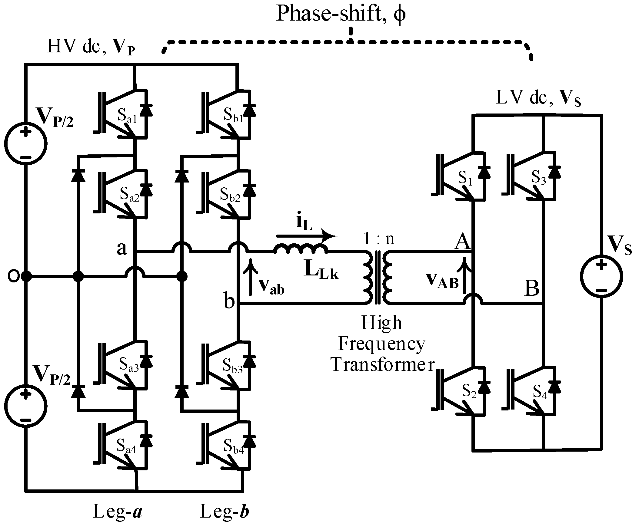
2. ML-DAB Topologies with Symmetric Phase-Shift Modulation
In this ML-DAB configuration, two bridges are assumed to have different dc voltage levels (
i.e.,
and
where
) where
and
are high and low dc bus voltages, respectively.
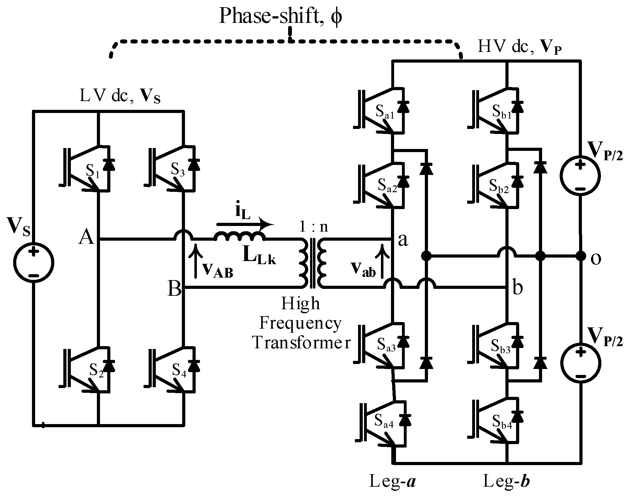
Figure 1 and
Figure 2 show voltage step-up and step-down schematics of NPC-based 2L-5L DAB, respectively. Most DAB-based power electronic converters deal with different voltage levels at the two ends of the converter, and this ML-DAB is very suitable for such applications. If the required voltage level is much higher than the dc bus voltage
, a higher voltage may be achieved by cascading multiple ML-DABs, which, in turn, facilitates conversion of large-scale (in the order of megawatts) power with a fewer number of ML-DAB modules. This methodology improves the overall efficiency and increases the power density.
Figure 1.
Boost configuration (Vp > Vs) of a multilevel dual active bridge (ML-DAB), where the transformer primary voltage (vAB) is two-level (2L) and the secondary (vab) of 5L.
Figure 1.
Boost configuration (Vp > Vs) of a multilevel dual active bridge (ML-DAB), where the transformer primary voltage (vAB) is two-level (2L) and the secondary (vab) of 5L.
Figure 2.
Buck configuration (Vs < Vp) of the ML-DAB where the transformer primary voltage (vab) is of 5L and the secondary (vAB) is of 2L.
Figure 2.
Buck configuration (Vs < Vp) of the ML-DAB where the transformer primary voltage (vab) is of 5L and the secondary (vAB) is of 2L.
2.1. Neutral Point Diode Clamped Configuration
The neutral point diode clamp (NPC) is one of the most popular and widely-used multilevel topologies in medium and high voltage industrial applications. In this ML-DAB, three-level (3L) diode clamped legs (leg-
a,
b in
Figure 1 and
Figure 2) are used to produce a leg-to-leg five-level (5L) voltage waveform
. The low voltage bridge is switched so as to produce a two-level (2L) square waveform
across the transformer. Compared to the 2L voltage source converter, the 3L-NPC configuration employs clamping diodes to connect the phase output to the neutral point “
o”, as shown in
Figure 1 and
Figure 2, which produces a 3L voltage at each NPC leg. The voltage sources (
i.e.,
) shown in
Figure 1 and
Figure 2 are practically replaced by bulk capacitors, and the input and/or the output of the ML-DAB usually are followed by a source, a load or other converters in real applications. This ML-DAB can be configured for single phase or three phases with bi-directional power-flow capability by using current bi-directional switches and a suitable modulation scheme. In this paper, we are analyzing different cases of ML-DAB assuming a single-phase transformer with unidirectional power flow from the 2L bridge to the 5L bridge. The bi-directional power flow can easily be controlled with the phase-shift angle (
) between the active bridges. Power always flows from the voltage-leading bridge to the voltage-lagging bridge.
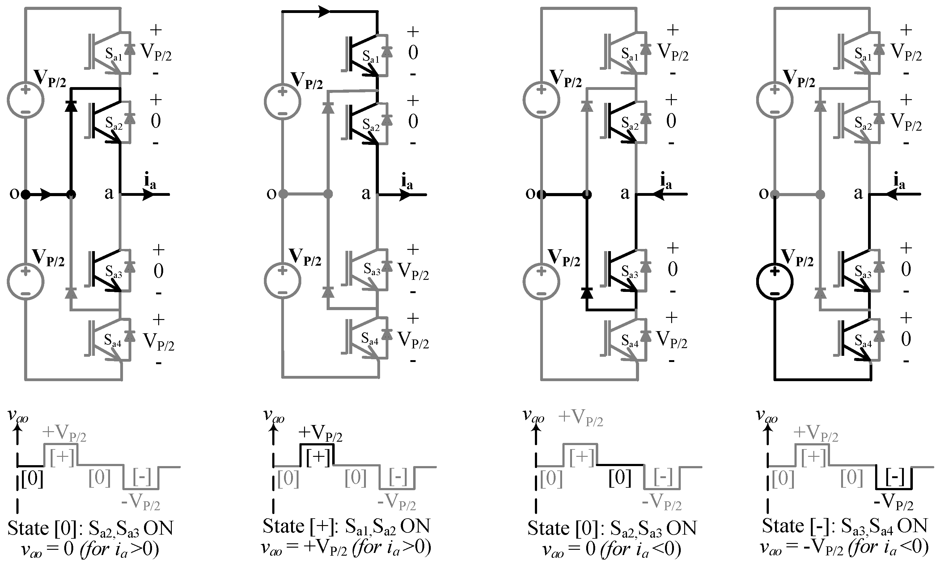
2.2. Switching States of the 3L-NPC Bridge
The NPC inverter concept was first proposed in 1980 [
15]. Since then, researchers have contributed to several aspects of this converter, such as various modulation schemes, the number of voltage levels, capacitor voltage balancing, harmonics mitigation and active clamping instead of diodes. Switching and modulation details of a 3L-NPC as a three-phase inverter are studied in detail in [
16]. In ML-DAB operation, the switching pattern of NPC is slightly different from that in conventional inverters. Unlike 3L-NPC line frequency (
i.e., 50 or 60 Hz) inverters, the switching frequency is considered the fundamental frequency in an ML-DAB.
Table 1 shows how a three-level voltage is synthesized in a 3L-NPC leg for both positive (
) and negative (
) current flow.
Table 1.
Switching states in a 3L-NPC leg.
Table 1.
Switching states in a 3L-NPC leg.
| Switching States | Status of the Switches in 3L-NPC Leg-a | 3-Level LEG Voltage, vao |
|---|
| Sa1 | Sa2 | Sa3 | Sa4 |
|---|
| + | ON | ON | OFF | OFF | + |
| 0 | OFF | ON | ON | OFF | 0 |
| − | OFF | OFF | ON | ON | − |
Figure 3 shows some major switching states to form a 3L (
i.e.,
) voltage waveform
. The main advantage of the 3L-NPC is that all of the switching devices in a leg withstand only half (
i.e.,
) of the dc bus voltage (
i.e.,
) during commutation between states, which also yields lower
in comparison to the two-level inverter. Switching between “+” and “−” states are not considered, because this scheme involves all four switches (
) in a leg, two being turned on and the other two being commutated off, during which dynamic voltage on each switch may not be kept the same [
16]. This also causes double the switching losses. A small dead time is allowed between different states. The leg-
b is also switched in a similar pattern to create a 3L voltage waveform
. In this proposed modulation scheme,
is phase-shifted from
by an amount
to produce a leg-to-leg 5L voltage waveform
across the transformer (
Figure 4).
Figure 3.
Switching states and corresponding 3L voltage (vao) synthesized from leg-a of a 3L-NPC bridge.
Figure 3.
Switching states and corresponding 3L voltage (vao) synthesized from leg-a of a 3L-NPC bridge.
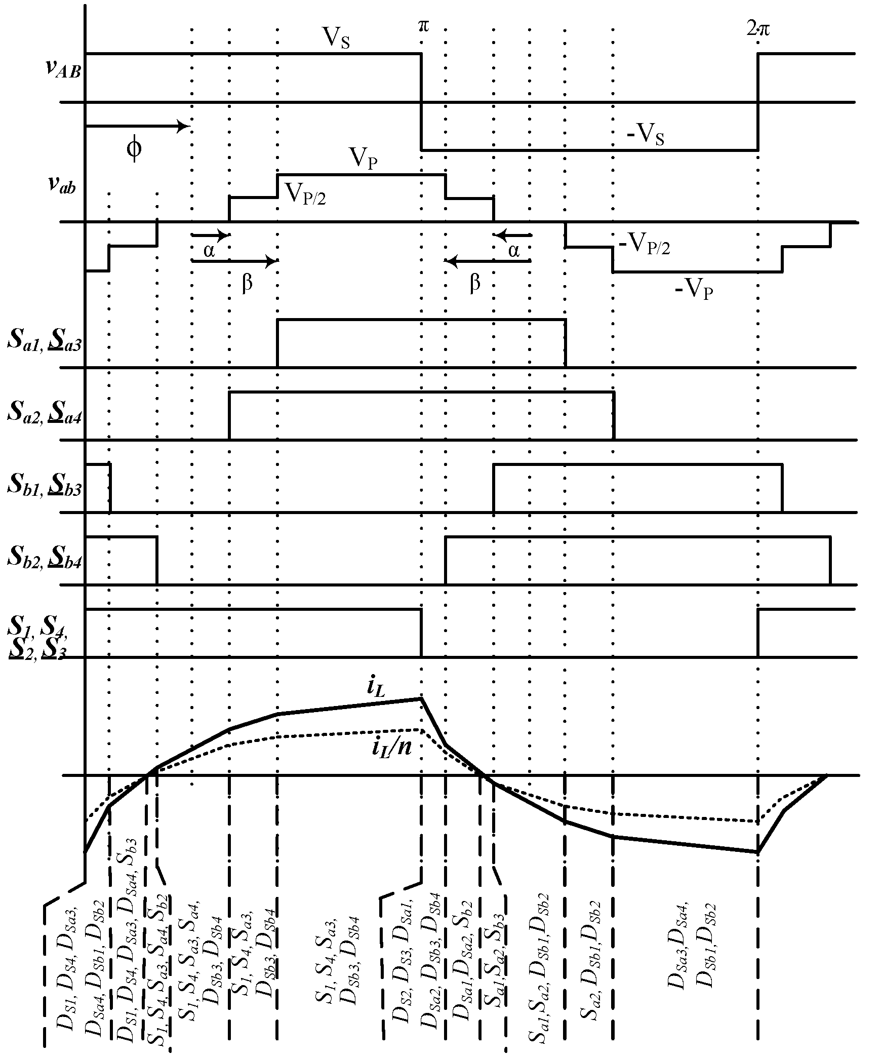
Figure 4.
Switch pulses and corresponding voltage waveforms and primary current in a 2L-5L DAB boost topology.
Figure 4.
Switch pulses and corresponding voltage waveforms and primary current in a 2L-5L DAB boost topology.
The two-level bridge has two legs, each having two complementary switches operating with a 50% duty cycle. When
are turned on, the leg-to-leg square wave voltage
, and when
are turned on,
. Gate pulses for all twelve switches (
i.e.,
) for both 2L and 5L bridges in a boost topology are shown in
Figure 4 with the resulting voltage waveforms (
) across the high frequency transformer and the current (
) through the leakage inductor.
2.3. Symmetric Modulation
In order to synthesize the 5L voltage
, the switching pulses and the resulting voltage waveform are defined with respect to angular distances (
i.e.,
) instead of the duty cycle. These angles
are measured symmetrically at zero,
and
within a switching period (
Figure 5). The zero and
are considered at the mid-point of the zero voltage level of the 5L voltage
. Defining
in such a symmetrical way is advantageous in terms of the minimum numbers of parameters (
) required, which, in turn, easily describe and derive a simple mathematical expression for power flow in the ML-DAB. These parameters
shape the multilevel voltage waveform and can be utilized in the improvement of the total harmonic distortion (THD) and voltage balancing of the capacitors [
14]. The phase-shift angle
is independent of
and acts as the control parameter to control the power flow in the ML-DAB.
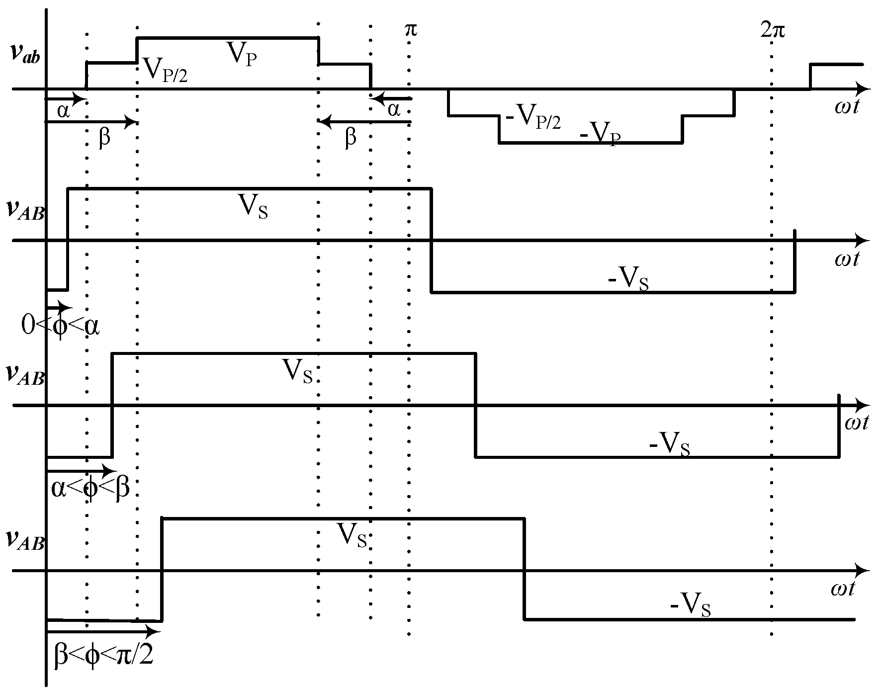
Figure 5.
Voltage waveforms in a 5L-2L DAB for three different cases of buck topology when vAB is formed using .
Figure 5.
Voltage waveforms in a 5L-2L DAB for three different cases of buck topology when vAB is formed using .
In order to produce a zero-average symmetric alternating waveform, the low-voltage (
) bridge legs should be switched complementarily at the duty cycle (
D) in a range of zero to 50% (
). If
, a 2L (
) voltage
will be formed, and if
, a 3L (
) voltage will be produced (
Figure 6). This 3L voltage at the low voltage bridge is also generated symmetrically, equally spaced from zero
by an angle
. This single parameter
can define the 3L
for the whole range of
.
Figure 6.
Voltage waveforms in a 3L-5L DAB boost topology when vAB is formed using
.
Figure 6.
Voltage waveforms in a 3L-5L DAB boost topology when vAB is formed using
.
3. Power Flow Equations and Soft Switching in ML-DAB
In ML-DAB, power flow is controlled by the phase-shift angle (
) between
and
, like conventional DAB. The leakage inductance of the high frequency transformer acts as the main energy transfer element. This primary referred leakage inductance is assumed externally as
in
Figure 1 and
Figure 2. In order to analyze the power flow through each type of ML-DAB shown in
Figure 4,
Figure 5 and
Figure 6, we will analyze the current
through the leakage inductor for each topology.
3.1. 2L-5L DAB Boost Topology
The switching and modulation for a 2L-5L DAB boost topology is shown in
Figure 4. The 2L
is assumed to start at angle zero, and 5L
is lagging
by the phase-shift angle
. From the basic inductor voltage relation we get,
One switching cycle time period has been converted to
2π radians in the following equations. Now, writing this
iL(θ) equation for each segment of
vL from zero to
π as shown in
Figure 4, we get,
Assuming zero average current through the transformer,
:
Putting this expression of
in the above equations, we can get the
at different points,
The average power flow expression from the primary to secondary bridge through the leakage inductance can be written as follows:
After calculating the above power equation using (3), we get the simplified power equation as follows,
where
is the average power (
is the per unit power) measured at the output of the converter with the variables defined as,
, where
is the switching frequency,
n is the transformer turns ratio,
m is the voltage conversion ratio defined as
and
L is the primary referred inductance (
) used at the high frequency link. The per unit power
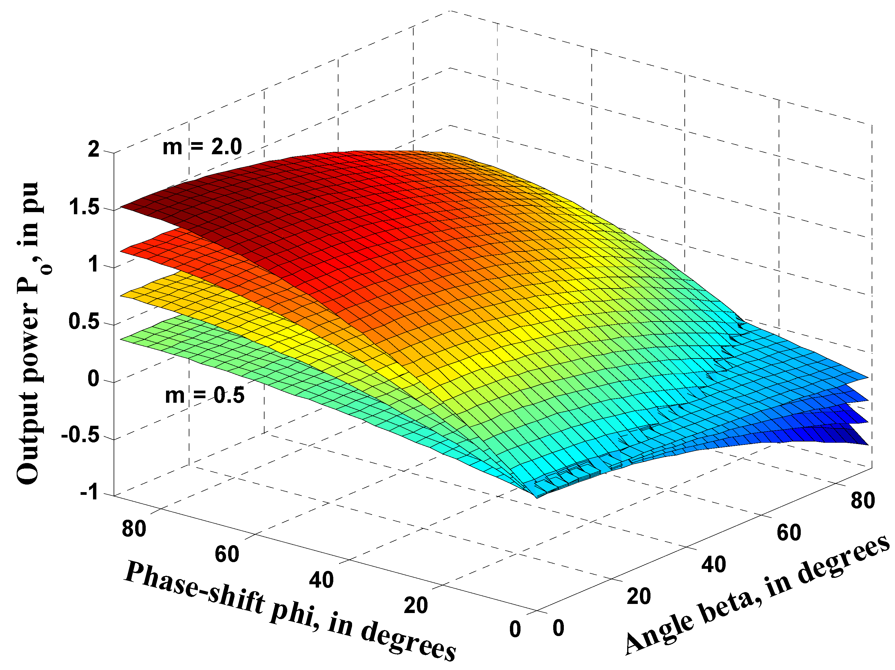
vs., while
α is chosen to be fixed at
, is shown in
Figure 7 for different
m values. Power
vs.
planes with different
m-values for a 2L-5L DAB boost topology are shown in
Figure 7.
Figure 7.
ML-DAB output power for
Figure 7.
ML-DAB output power for
3.2. 5L-2L DAB Buck Topology
The voltage waveforms for a 5L-2L DAB buck topology are shown in
Figure 5. The 5L
vab is assumed to start at angle zero, and 2L
vAB is lagging by the phase-shift angle
ϕ. In this topology, based on the value of
ϕ, there may be three cases, such as
. Each case has been analyzed to formulate a power flow equation using the same procedure described from (1) to (11).
Equation (14) may be considered as the generalized one and can be rewritten as follows,
Equations (10) and (15) are the same, which also validates the bi-directional power-flow capability of this ML-DAB converter only based on the phase-shift between primary and secondary side bridge voltages.
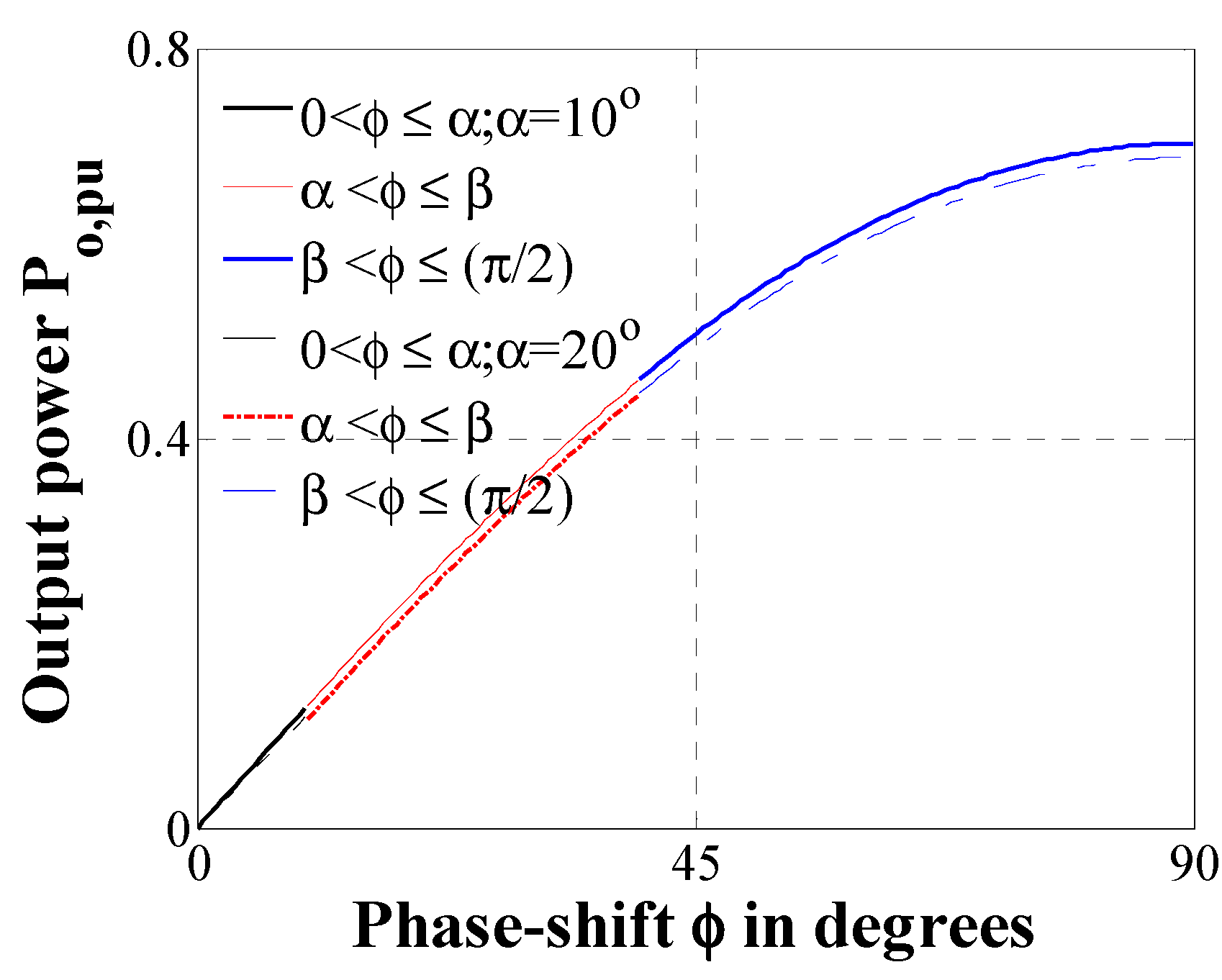
Figure 8 shows the power flow from the 5L to 2L bridge for the three different cases described above.
Figure 8.
Power flow through DAB for all three cases (12) to (14), with respect to phase-shift ϕ; here,
are assumed for calculation.
Figure 8.
Power flow through DAB for all three cases (12) to (14), with respect to phase-shift ϕ; here,
are assumed for calculation.
3.3. 3L-5L DAB Boost Topology
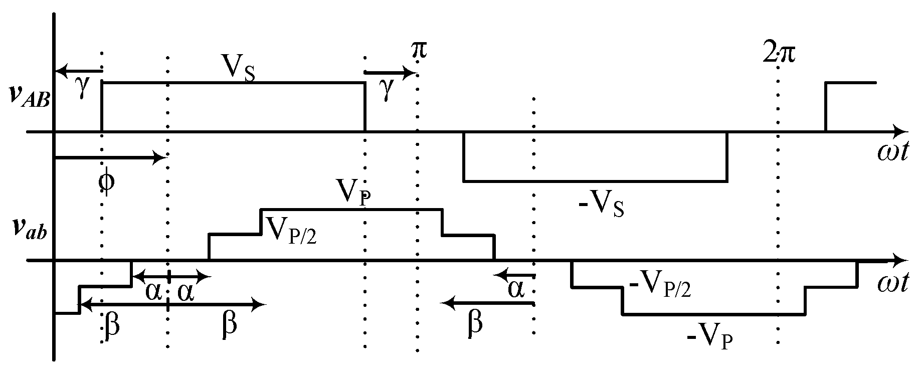
The primary and secondary voltage waveforms for a 3L-5L DAB boost topology are shown in
Figure 9. The 3L
vAB is assumed to start at angle
γ after the zero, and 5L
vab is lagging
vAB by the phase-shift angle
ϕ The pulse-width of 3L waveform is assumed symmetrically reduced by an angle of
γ which actually results from switch duty cycles
D < 5. Using the same sector-wise inductor current analysis, as shown in (1) to (10), the power flow equation for this topology has been derived as,
If we put
in (16), it reduces to the 2L-5L power equation in (11). Similarly, if the condition is such that
, Equations (11) and (16) reduce to the conventional two-level DAB onverter equations [
1].
Figure 9.
Primary 3L voltage vAB secondary 5L voltage vab and current through the primary referred leakage inductance iL; where
Figure 9.
Primary 3L voltage vAB secondary 5L voltage vab and current through the primary referred leakage inductance iL; where
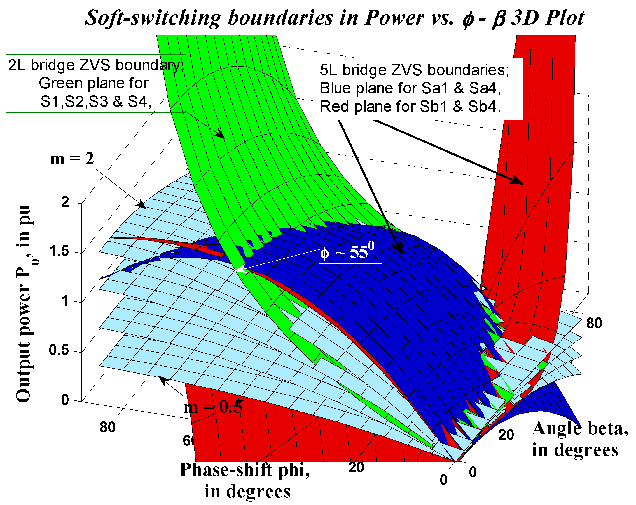
3.4. Soft Switching
The per unit output power
vs.
characteristics is shown in
Figure 10 (15), where
is chosen as
, as this value gives the minimum THD in five-level
[
14]. In
Figure 11, the two-dimensional view of
-
planes ease the visualization of the boundary values of
for achieving soft-switching both in primary (2L) and secondary (5L) bridges, as described in the following subsections.
Figure 10.
Soft switching boundaries shown in three-dimensional power vs. -
planes (where
); the grey planes (15) show the power vs. phi-beta relations for m = 0.5, 1, 1.5, 2; the green plane (17) is for two-level bridge, and the zero voltage switching (ZVS) is possible while operating under this plane; the blue (18) and red (19) planes are for five-level bridge leg-a and leg-b, respectively.
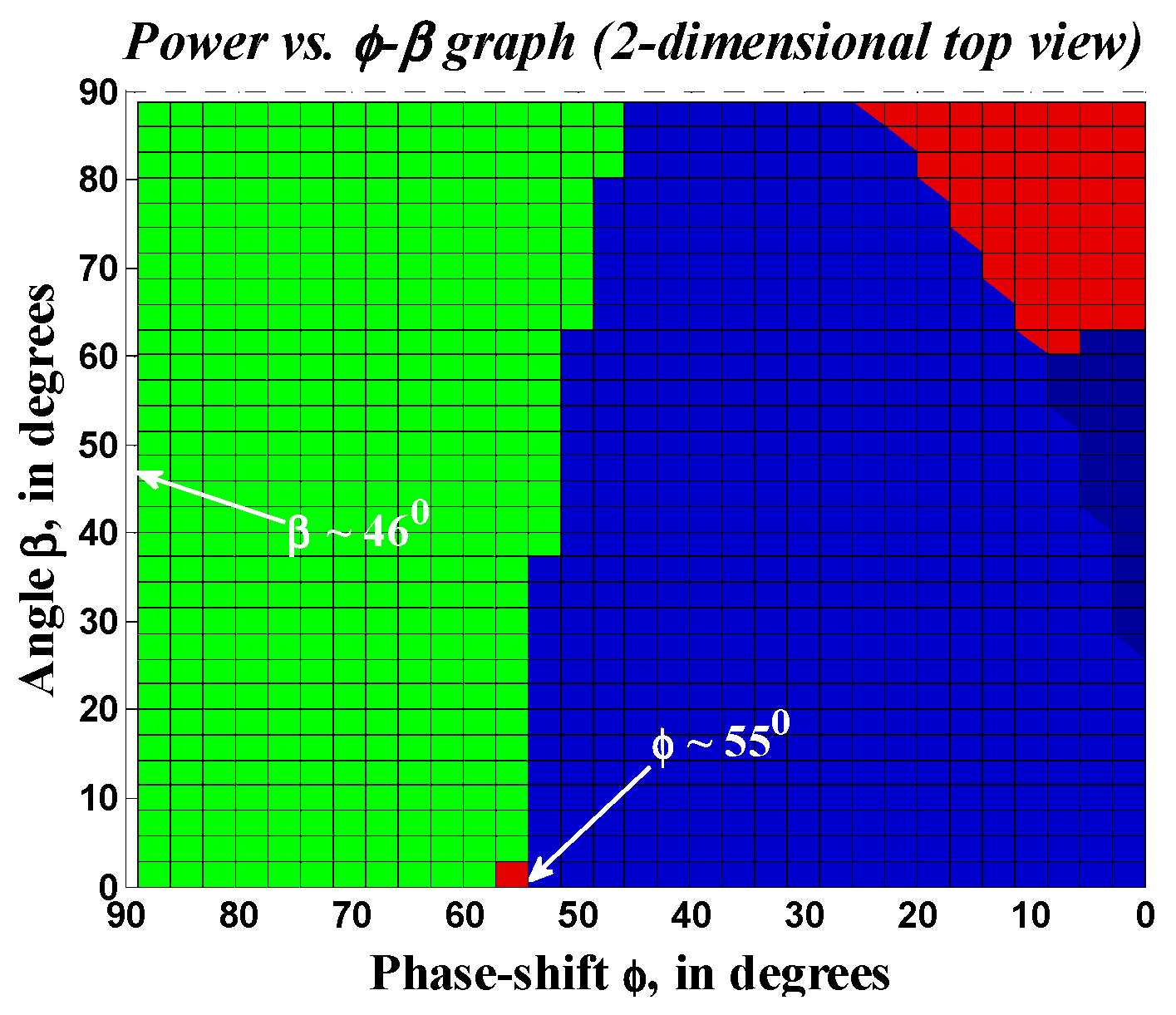
Figure 11.
Two-dimensional view of
Figure 10 showing the ZVS boundaries of
ϕ and
β.
Figure 11.
Two-dimensional view of
Figure 10 showing the ZVS boundaries of
ϕ and
β.
The conventional 2L DAB topology can achieve zero voltage switching (ZVS) for all switches in the entire power range when
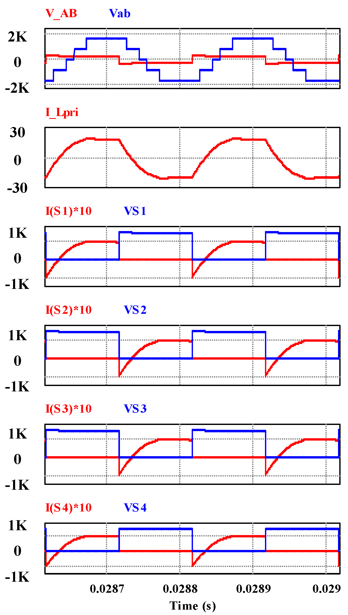
m is equal to unity. The switching pulses for the 2L-5L DAB switches are shown in
Figure 4. It is possible to achieve the same in the primary bridge (
S1 to
S4 with the condition of
as shown in
Figure 12.
3.4.1. Soft-Switching Conditions for the Two-Level (Vs) Bridge
From the current and voltage waveform of the switches in the primary two-level (V
s) bridge (
Figure 12), we can say that the condition for soft-switching in the primary bridge should be,
Figure 12.
Voltage across the transformer vAB and vab, inductor current iL and switch currents and voltages for S1 to S4.
Figure 12.
Voltage across the transformer vAB and vab, inductor current iL and switch currents and voltages for S1 to S4.
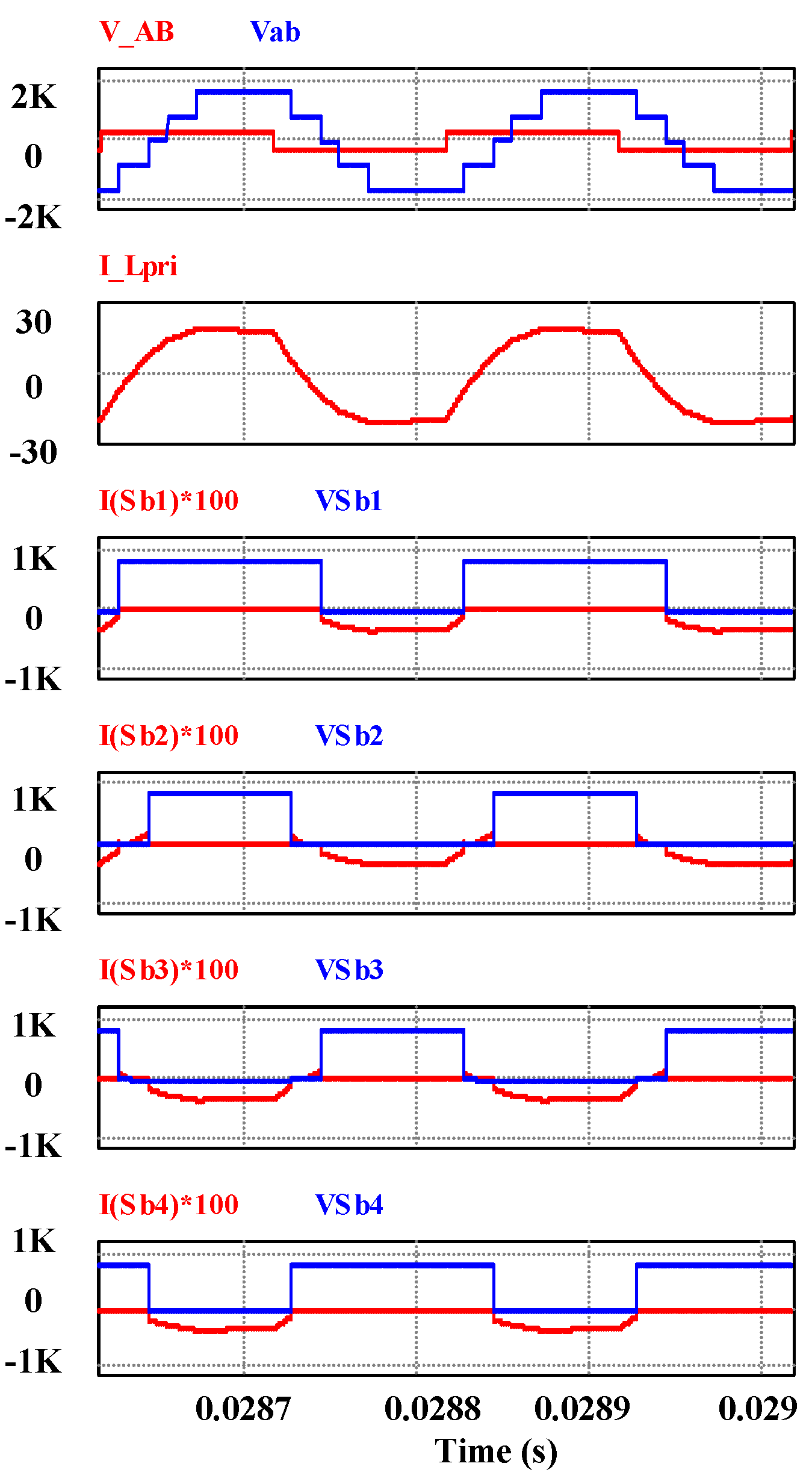
3.4.2. Soft-Switching Conditions for the Leg-a of NPC (Five-Level) Bridge
Condition for S
a1 and S
a4 to be turned-on at ZVS:
Boundary condition for S
b1 and S
b4 to be turned-on at ZVS:
In the NPC bridge, ZVS happens in the switches
during turn-on at
. The rest of the switches
are also turned on at a favorable condition when the current through the switch is already zero, as shown in
Figure 13 and
Figure 14.
Figure 13.
Voltage across the transformer , inductor current
and switch currents and voltages for
to
.
Figure 13.
Voltage across the transformer , inductor current
and switch currents and voltages for
to
.
Figure 14.
Voltage across the transformer vAB vab, inductor current iL and switch currents and voltages for Sb1 to Sb4.
Figure 14.
Voltage across the transformer vAB vab, inductor current iL and switch currents and voltages for Sb1 to Sb4.
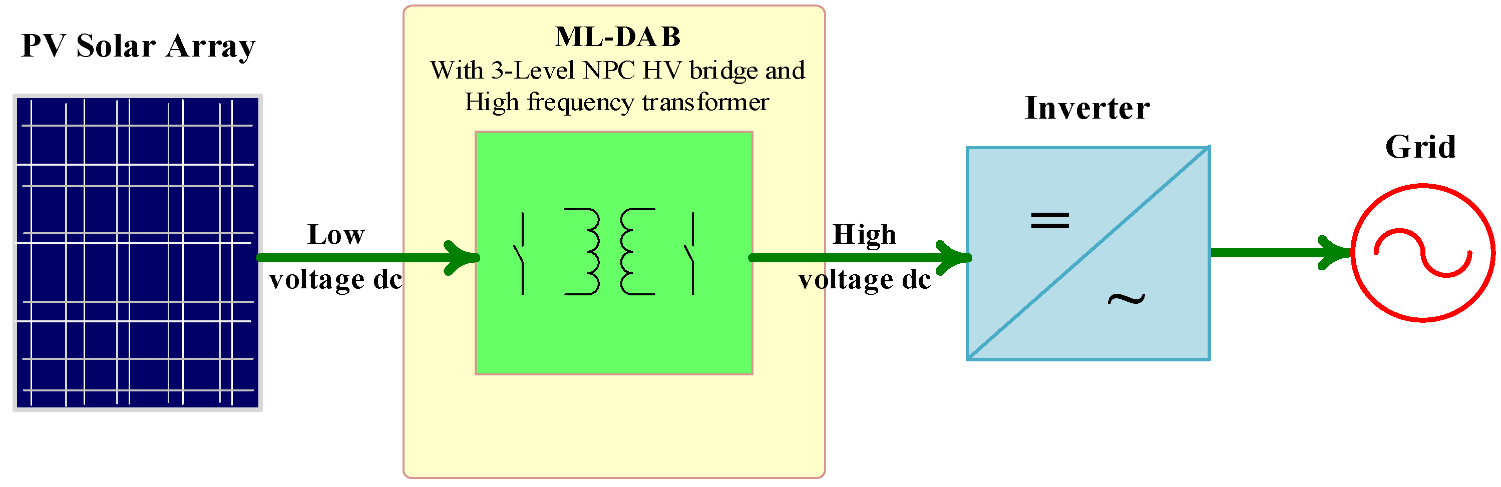
4. Applications for ML-DAB
The proposed ML-DAB could find some suitable applications in a solid state transformer (SST), a front-end DC-DC converter in a photovoltaic (PV) system, a high step-up voltage DC-DC or an intermediate stage in ac-ac applications.
Figure 15 shows a block diagram of the ML-DAB in a grid-connected large-scale PV system. The ML-DAB module along with inverter stage can act as a building block to be cascaded in order to achieve the 13.8-kV distribution voltage requirement.
Figure 15.
ML-DAB module in a grid-connected photovoltaic (PV) power converter.
Figure 15.
ML-DAB module in a grid-connected photovoltaic (PV) power converter.
This ML-DAB can control maximum power point tracking (MPPT) by controlling the phase-shift (
) between two active bridges. This topology has the advantage of being modular and replacing the bulky line frequency transformer at the grid-end with a smaller high frequency power electronic transformer.
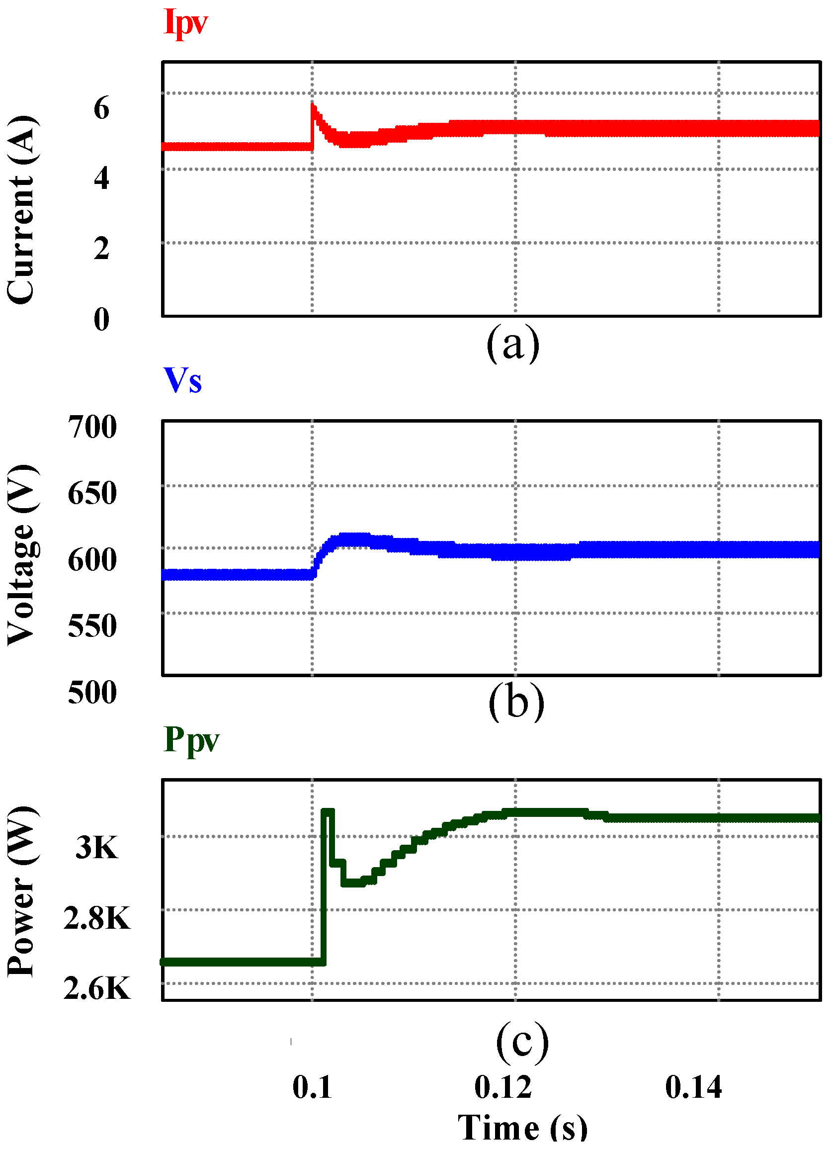
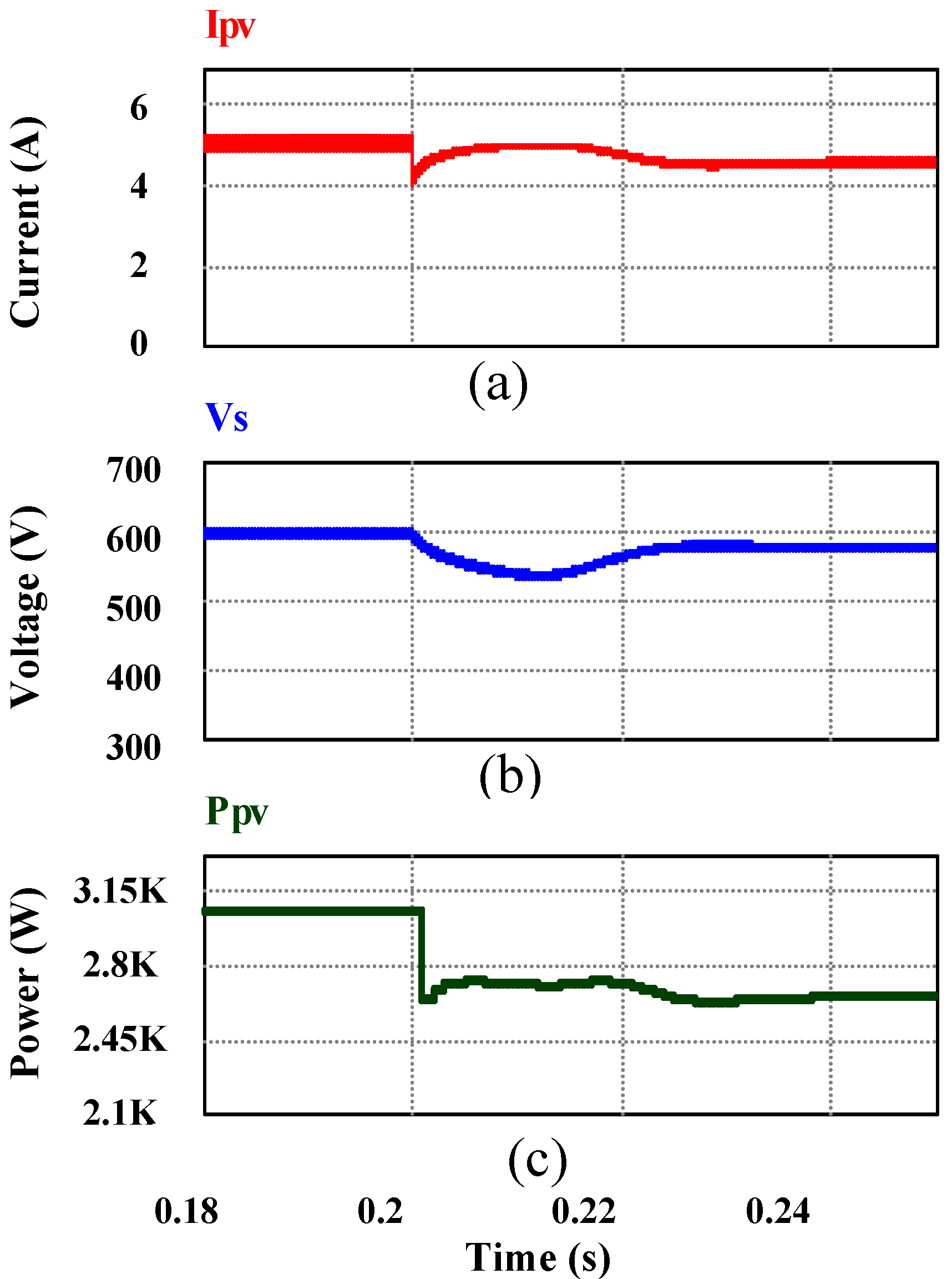
Figure 16,
Figure 17 show the MPPT performance in an ML-DAB in PV applications.
Figure 16.
(From top to bottom) (a) Change in PV output current Ipv due to the change in light intensity from 800 W/m2 to 1,000 W/m2; (b) corresponding change in voltage Vpv because of maximum power point tracking (MPPT) and (c) power Ppv.
Figure 16.
(From top to bottom) (a) Change in PV output current Ipv due to the change in light intensity from 800 W/m2 to 1,000 W/m2; (b) corresponding change in voltage Vpv because of maximum power point tracking (MPPT) and (c) power Ppv.
Figure 17.
(From top to bottom) (a) Change in PV output current Ipv due to the change in light intensity from 1,000 W/m2 to 800 W/m2; (b) corresponding change in voltage Vpv because of MPPT and (c) power Ppv.
Figure 17.
(From top to bottom) (a) Change in PV output current Ipv due to the change in light intensity from 1,000 W/m2 to 800 W/m2; (b) corresponding change in voltage Vpv because of MPPT and (c) power Ppv.
5. Simulation and Experimental Results
A 3.34-kW ML-DAB module with a single phase high frequency transformer has been simulated in PSIM
®. The design parameters of the ML-DAB are listed in
Table 2. Based on the soft-switching constraints for the ML-DAB switches, as shown in (16) to (19), a good choice for modulation parameters is used for simulation, which are
and
. For the PV application explained in
Section 4, 1,200-V or 1,700-V rated IGBTs are needed for ML-DAB. There are limitations in the switching characteristics of commercially available IGBTs when operated above 20 kHz. Hence, we have chosen 5 kHz for the proposed ML-DAB. The minimum input capacitor value has been theoretically calculated as 39 uF based on the ML-DAB parameters in
Table 2. In the prototype, we have used a 100-uF polypropylene capacitor with a high ripple current carrying capacity.
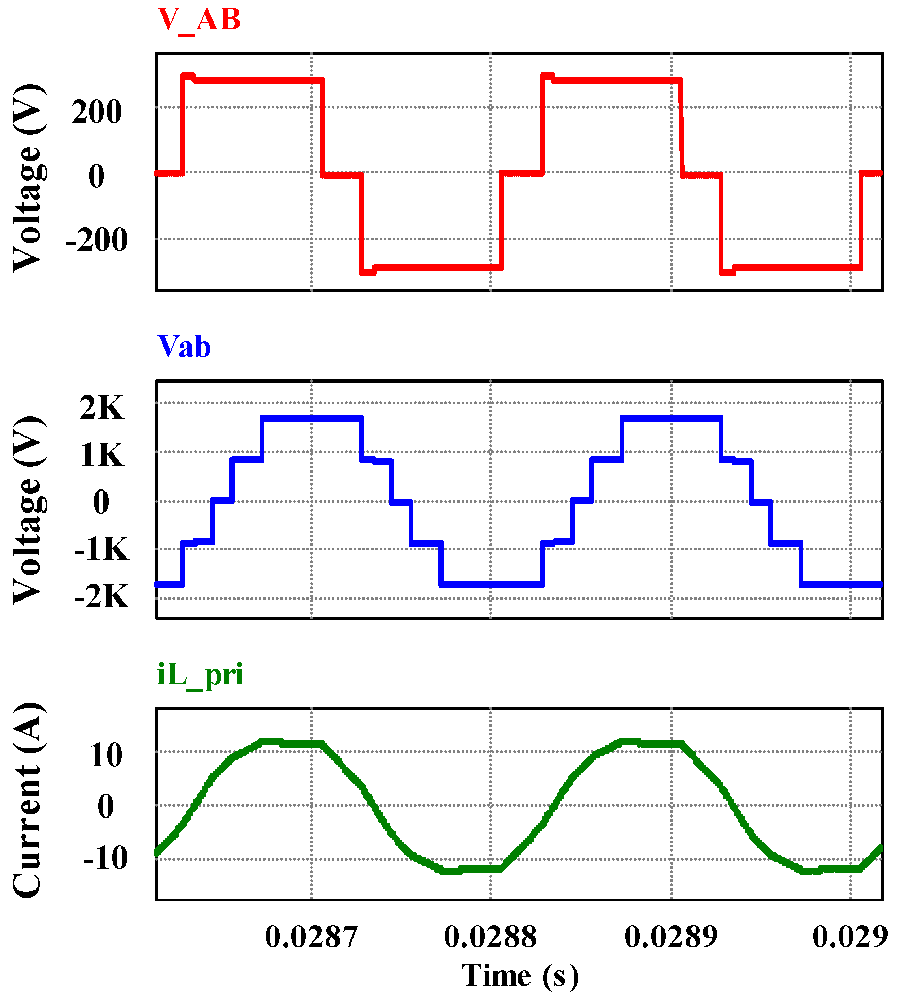
As per (10) and
Table 2, the key simulation results are shown in
Figure 18 and
Figure 19 for a 2L-5L DAB in the steady state. The corresponding voltage and current waveforms for the 3L-5L ML-DAB have been shown in
Figure 9 for the same input, output dc voltage and power rating as shown in
Table 2. The phase-shift
ϕ is actually the control parameter that is controlled by a proportional-integral (PI) controller sensing the variation in input (e.g., the PV panel’s output) or output (e.g., the input voltage of an inverter) dc voltages of the ML-DAB.
Figure 18 and
Figure 19 show the input and output voltage, current and average power of the ML-DAB obtained from simulation.
Table 2.
Parameter values for a 3.34-kW ML-DAB based on the 2L-5L topology.
Table 2.
Parameter values for a 3.34-kW ML-DAB based on the 2L-5L topology.
| Item Description | Nominal Value |
|---|
| Power rating of a ML-DAB module, Po | 3.34 kW |
| Vs = Vdc(2L) | 292 V |
| VP = Vdc(5L) | 1,668 V |
| ML-DAB high frequency transformer’s turns ratio, | 5.716 |
| 11.4 A |
| 2 A |
| 17 A |
| Switching frequency, fs | 5 kHz |
| Leakage Inductance for ML-DAB transformer, L (value calculated as per Equation 14) | 0.5 mH |
| 2-level PV side bridge IGBT’s VCE | 600 V (49% of Vs) |
| 3-level NPC bridge IGBT’s VCE | 1,200 V (70% of ) |
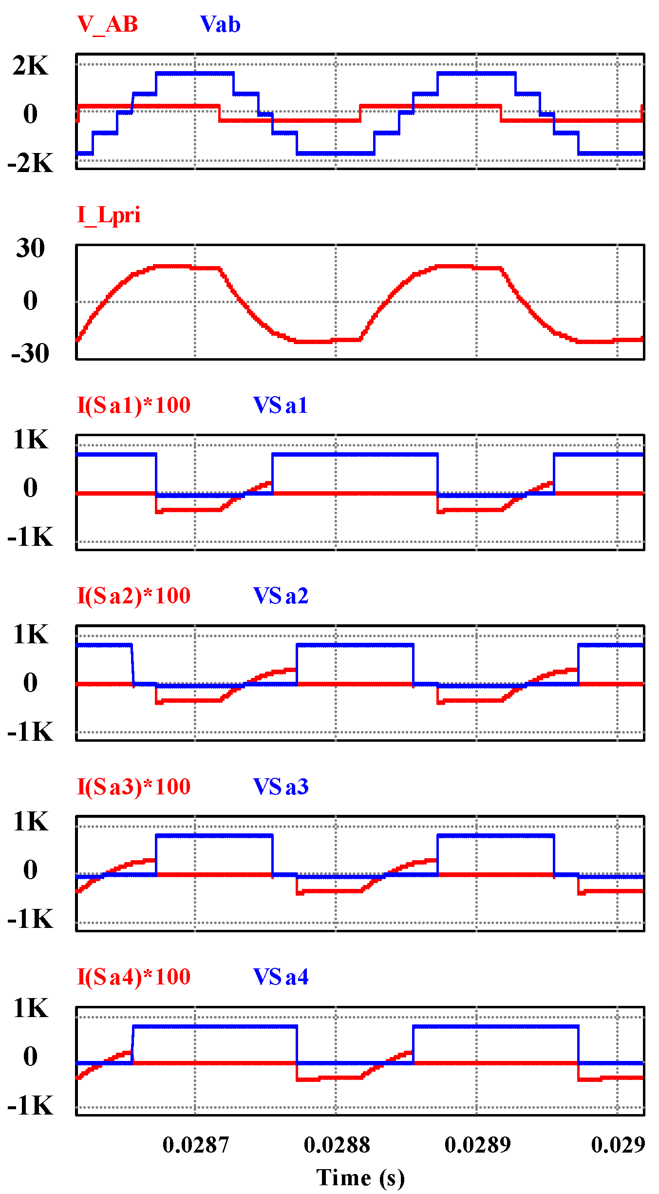
Soft-switching results for semiconductor switches in the converter are shown in
Figure 12,
Figure 13 and
Figure 14 showing zero voltage switching (ZVS) and zero current switching (ZCS) performance. Infineon 1,200-V IGBT modules FF100R12YT3 are modeled in the simulation to estimate the losses and efficiency. In the simulation, the conduction losses have been modelled based on the IGBT datasheet parameters and assuming linear switching characteristics. The efficiency is 96.42%, as seen in the simulation.
Figure 18.
(From top to bottom) (a) Primary 2L voltage vAB; (b) secondary 5L voltage vab; and (c) current through the primary referred leakage inductor iL.
Figure 18.
(From top to bottom) (a) Primary 2L voltage vAB; (b) secondary 5L voltage vab; and (c) current through the primary referred leakage inductor iL.
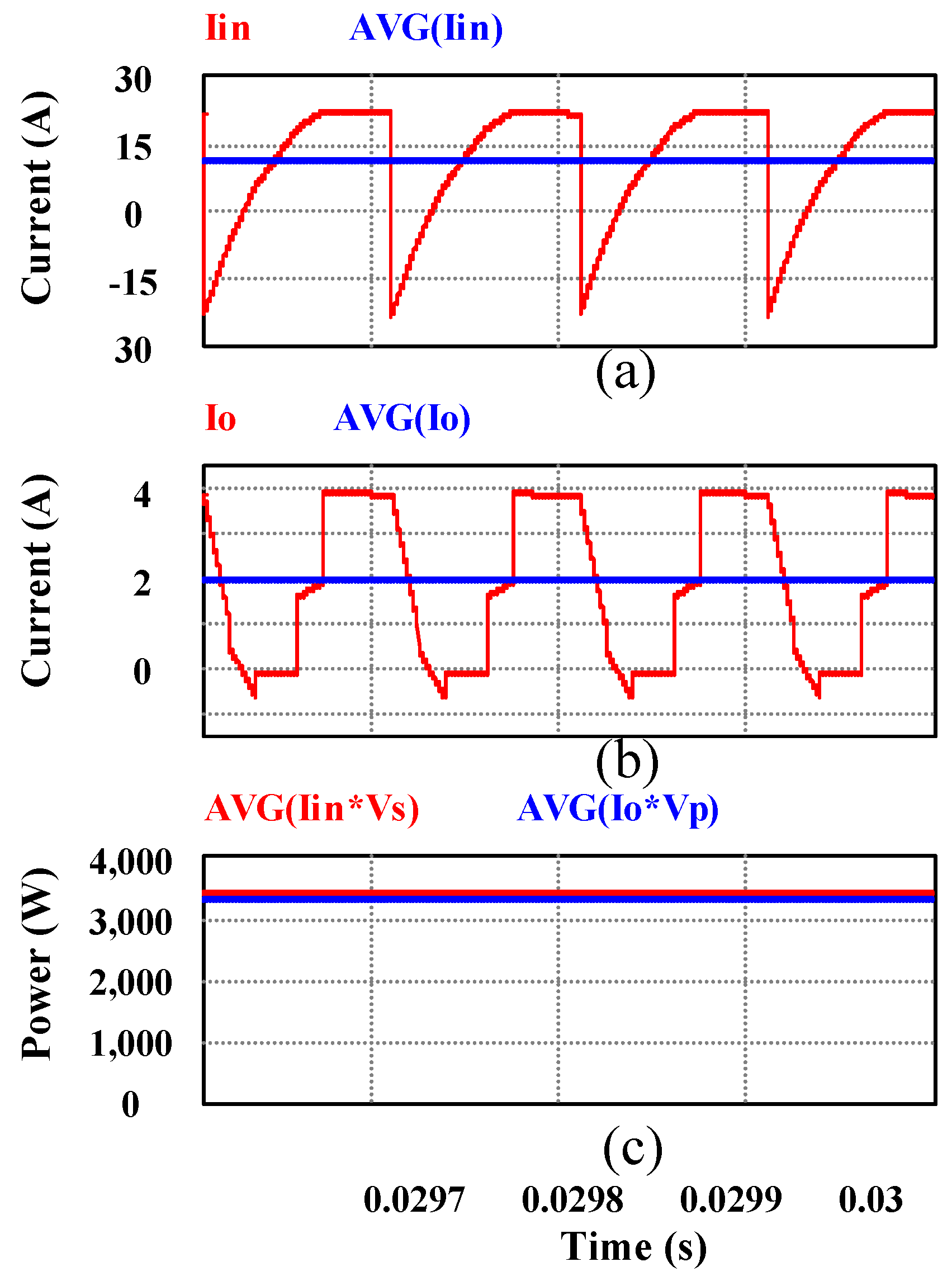
Figure 19.
(From top to bottom) (a) ML-DAB input current Iin and its average; (b) output current Iout and its average; and (c) average input and output power .
Figure 19.
(From top to bottom) (a) ML-DAB input current Iin and its average; (b) output current Iout and its average; and (c) average input and output power .
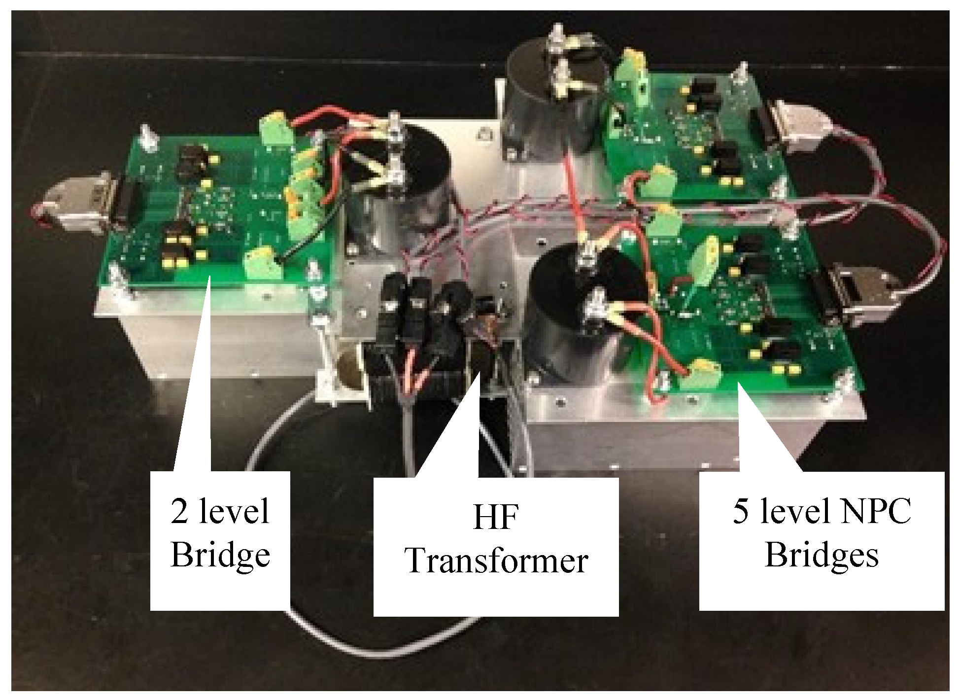
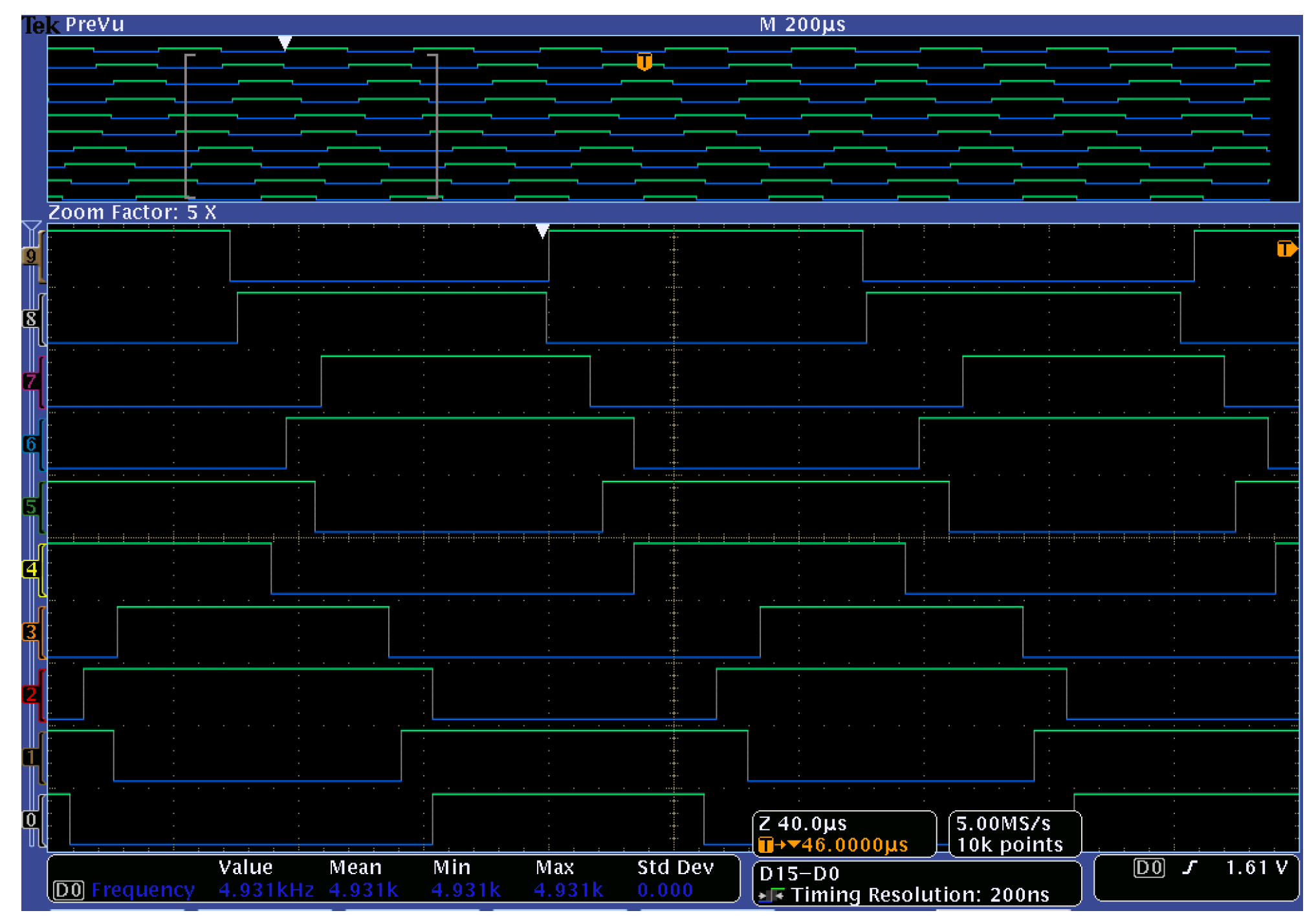
Simulation and experimental results also verify the functionality of the proposed ML-DAB and the symmetric modulation technique. A hardware prototype (
Figure 20) has been built and tested with a scaled-down input voltage (
) to verify the power flow and open-loop control. The gate signal for all the twelve IGBTs used in the ML-DAB is shown in
Figure 21.The experimental voltage and current waveforms shown in
Figure 22 and
Figure 23 have a close match with the simulation results shown in
Figure 18 and
Figure 19.
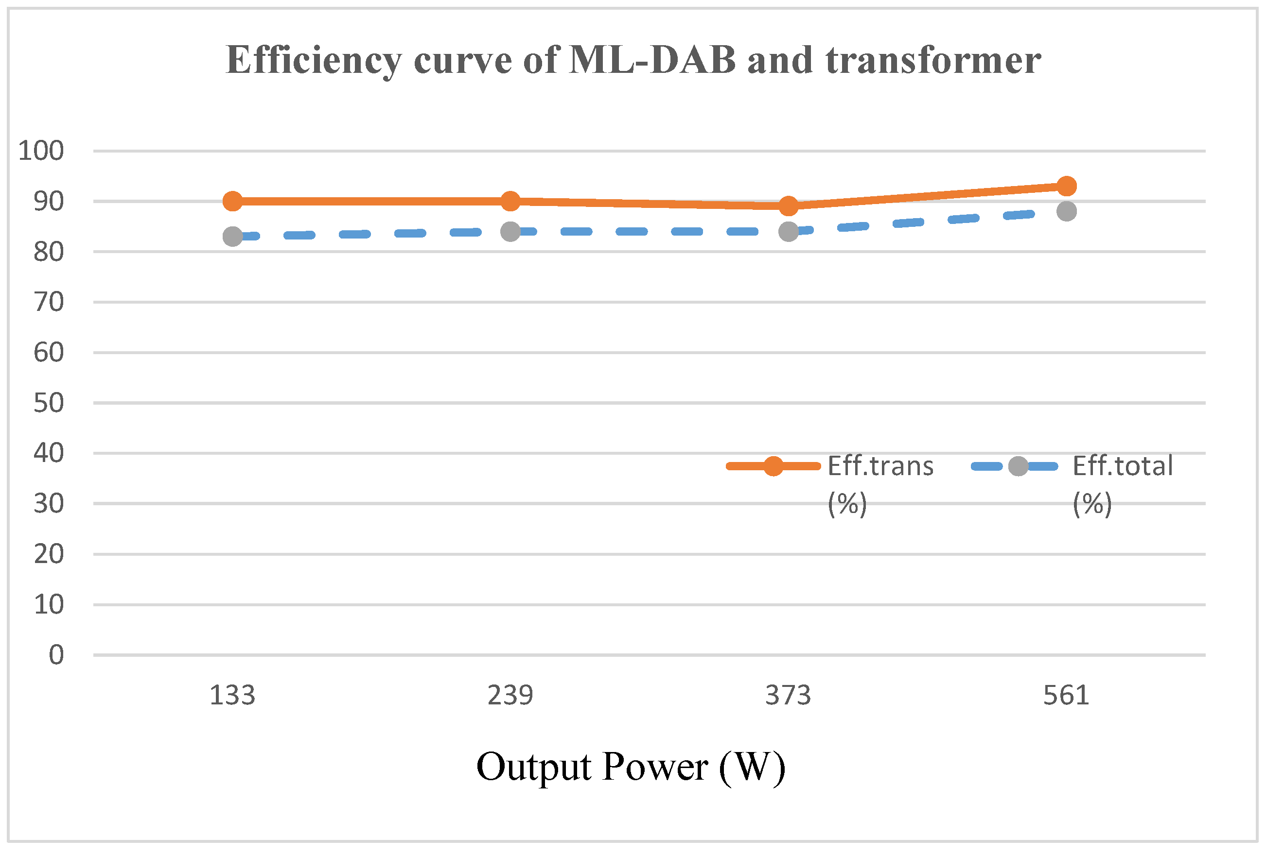
Figure 24 shows the output voltage and current waveforms when the ML-DAB is connected to a full-bridge inverter and a resistive-inductive (R-L) load. In the hardware prototype, an overall efficiency of 88% (
Figure 25) has been observed for a 120-V input voltage and 638 W (which is 20% of the rated power of the converter) of input power (
Table 3). At full rated power, it is expected that the observed efficiency will closely match with the theoretical and simulated efficiency figures.
Figure 20.
ML-DAB prototype hardware setup for laboratory testing.
Figure 20.
ML-DAB prototype hardware setup for laboratory testing.
Figure 21.
Gate pulses for the ML-DAB IGBTs (from top to bottom:
.
Figure 21.
Gate pulses for the ML-DAB IGBTs (from top to bottom:
.
Table 3.
Experimental efficiency and losses for the prototype ML-DAB.
Table 3.
Experimental efficiency and losses for the prototype ML-DAB.
| Vs | Vp | Pin | Pout | | | Efftrans | Efftotal |
|---|
| (V) | (V) | (w) | (w) | (w) | (w) | (%) | (%) |
|---|
| 60 | 310 | 161 | 133 | 14 | 28 | 90 | 83 |
| 80 | 416 | 284 | 239 | 27 | 45 | 90 | 84 |
| 100 | 521 | 443 | 373 | 45 | 70 | 89 | 84 |
| 120 | 626 | 638 | 561 | 42 | 77 | 93 | 88 |
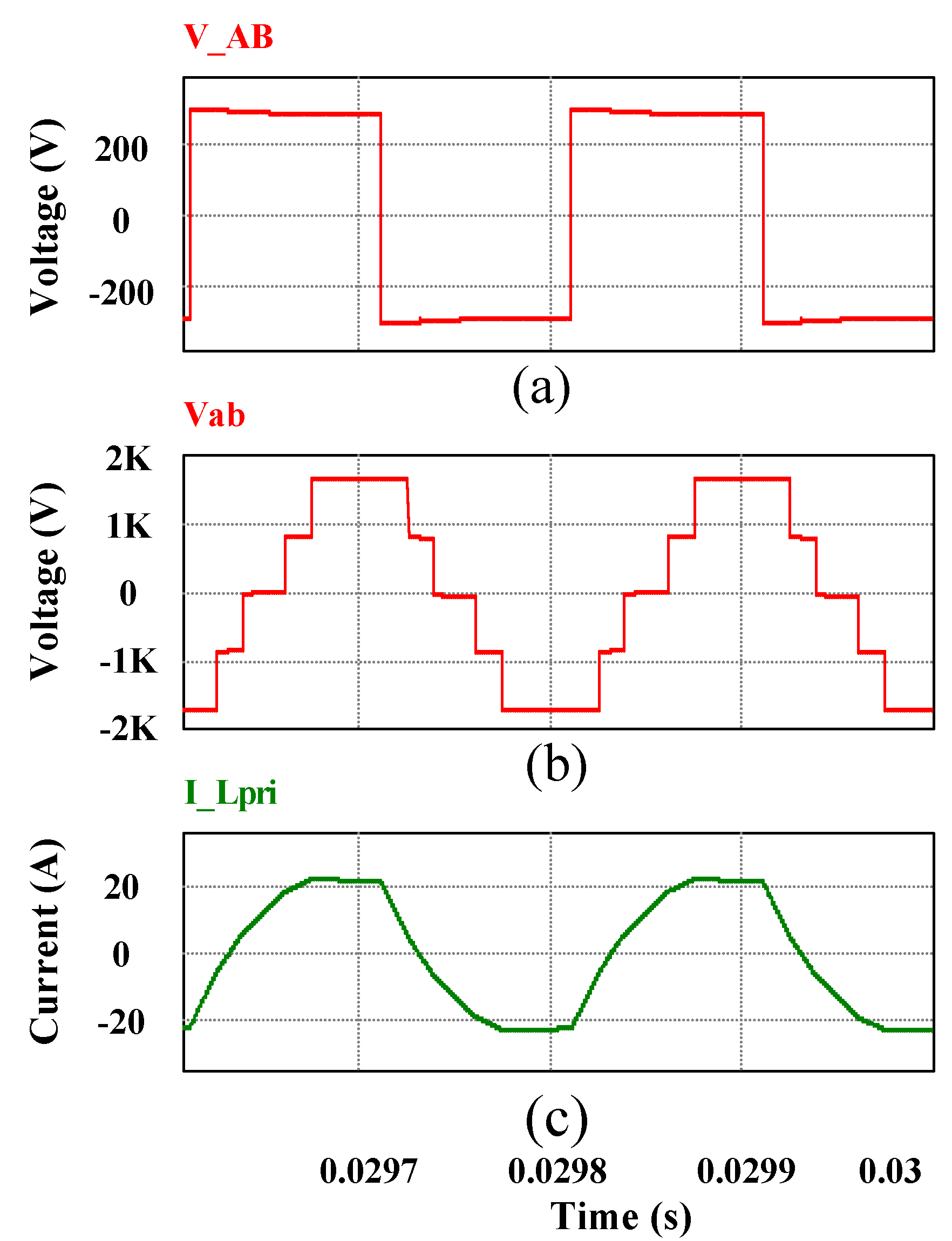
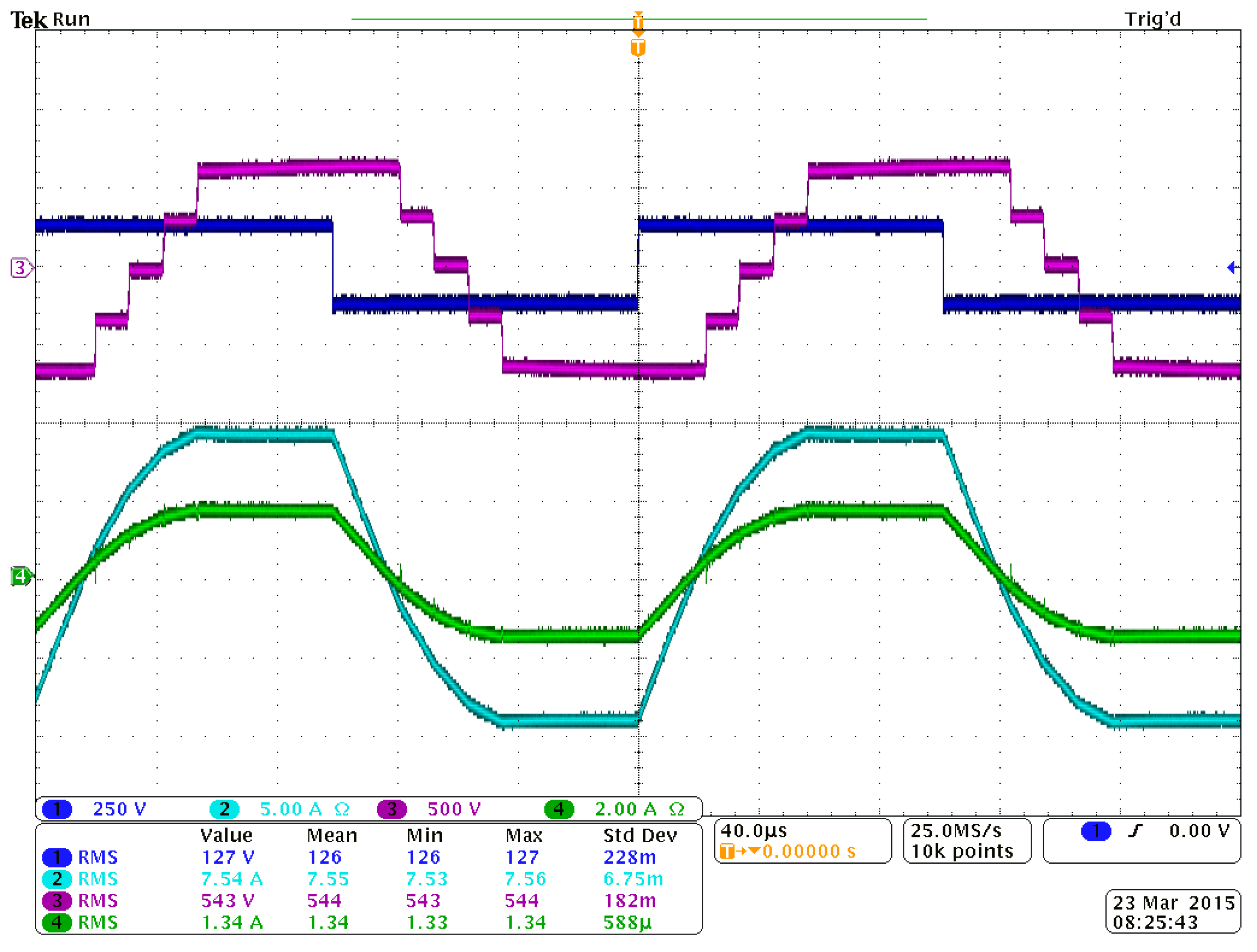
Figure 22.
ML-DAB 2L voltage vAB, 5L voltage vab and current through the 2L and 5L side of the transformers
; where
Figure 22.
ML-DAB 2L voltage vAB, 5L voltage vab and current through the 2L and 5L side of the transformers
; where
Figure 23.
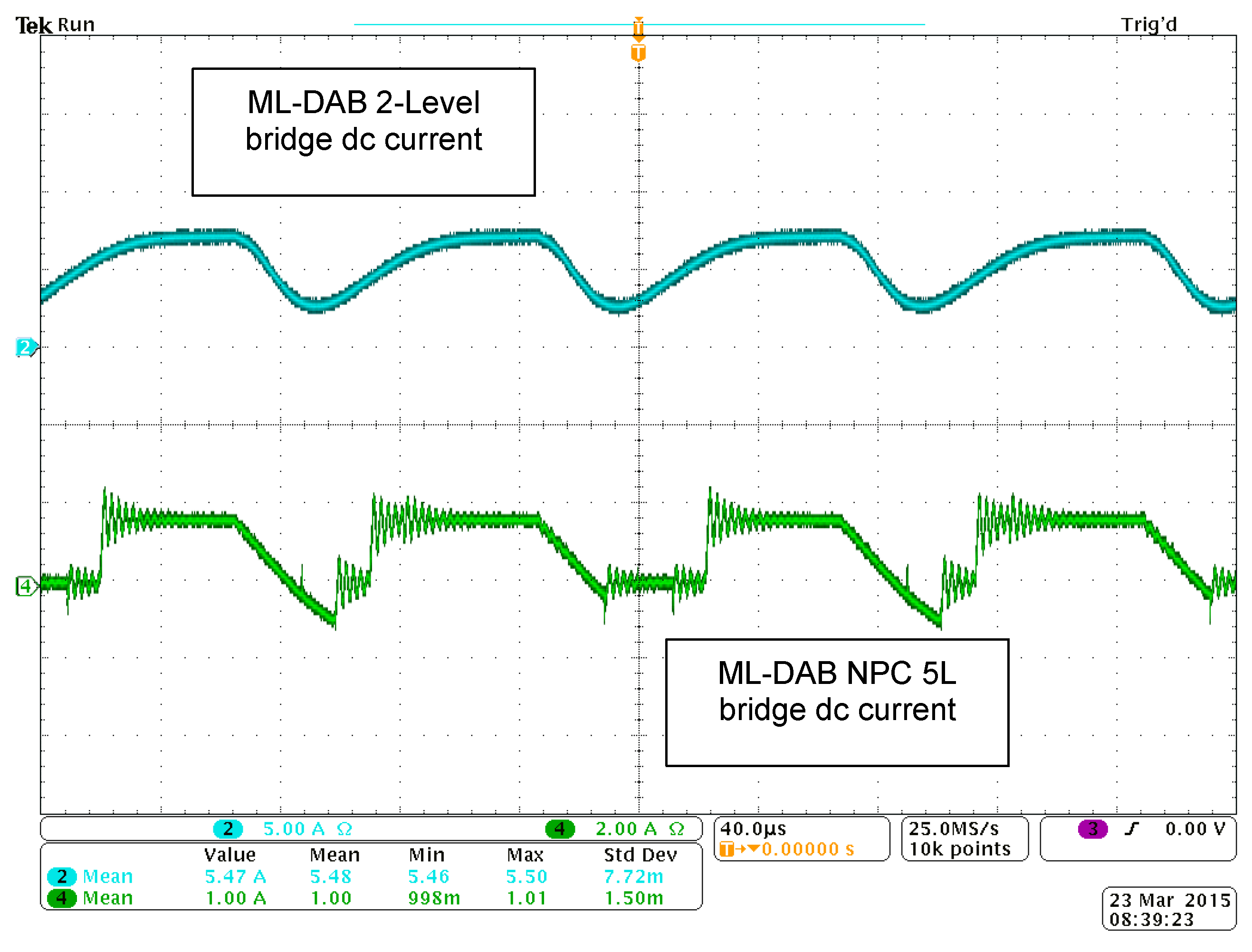
ML-DAB input (2L bridge) and output (5L bridge) dc current waveforms
and
Figure 23.
ML-DAB input (2L bridge) and output (5L bridge) dc current waveforms
and
Figure 24.
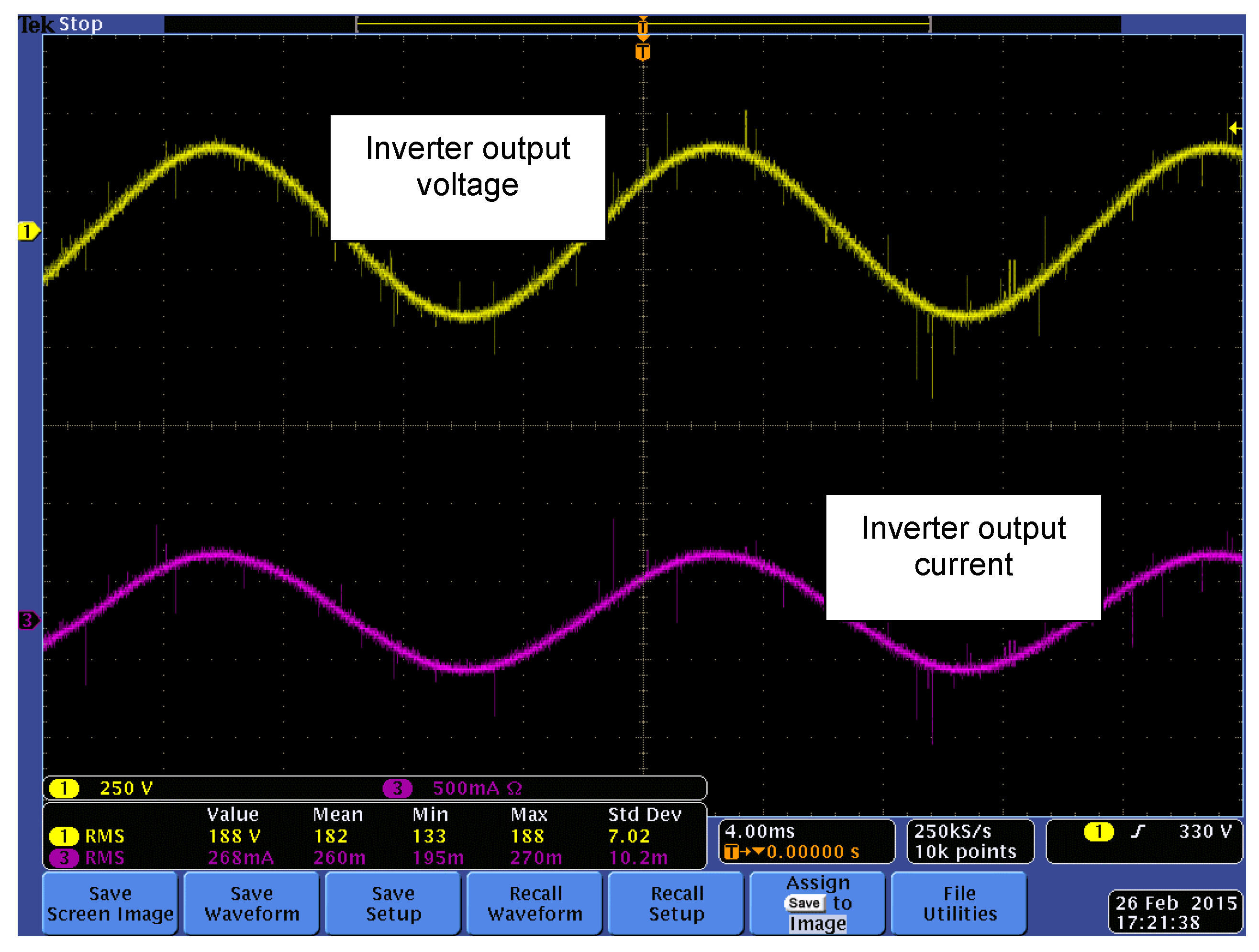
Output voltage and current waveforms when the ML-DAB is connected to a full-bridge inverter and a resistive-inductive (R-L) load.
Figure 24.
Output voltage and current waveforms when the ML-DAB is connected to a full-bridge inverter and a resistive-inductive (R-L) load.
Figure 25.
Efficiency curve of the transformer and ML-DAB with output power variation.
Figure 25.
Efficiency curve of the transformer and ML-DAB with output power variation.


