3. Theoretical Analysis and Discussion
The Fourier transform
S(
f) of a continuous time-domain signal
x(
t) is defined as:
where
t is time. Theoretically,
x(
t) is a continuous function of time. By practical necessity,
x(
t) can only be observed for a limited duration in time in real-life implementations. By the same necessity, even within this limited duration in time
x(
t) cannot be observed as a continuum—only sampled a limited number of times, at certain moments in time. Therefore, since only a limited set of “instantaneous” observations of the function value can be obtained within a limited time interval, in real life the Fourier transform above can only be approximated. Additional analysis must be undertaken to ensure that this approach produces a reasonably accurate approximation of the theory for a set of criteria relevant to a specific application.
This limited set of observations is usually referred to as a sampled input signal
x(
k) of a certain total length
N, where
k is an index of the samples of an input signal vector of dimension
N. Assuming that the input signal is observed at equal intervals of time, the discrete approximation of the Fourier transform over a finite duration is defined as:
In the DFT literature, the exponent term may be referred to as the “analysis” or “test” phasor, the integer m, as the analysis or test frequency and 1/N as the fundamental frequency. The test phasor is a periodic function of k that completes m cycles as k goes from 0 to N−1 in the summation. Both the sampled input signal x(k) and the sampled test phasor can be considered vectors of dimension N and the sum above is essentially the inner product of these two vectors. Therefore, the sum can be considered a projection of the sampled input vector x(k) onto a sampled test phasor at a given m.
A set of sampled test phasors
at various integers
m forms an orthogonal basis [
2]. The sampled input vector
x(
k) therefore can be decomposed into a set of projections along these basis vectors (harmonics). If the direction of the input vector
x(
k) happens to coincide with one of the basis vectors at a certain
m, only a single projection onto this vector basis is a non-zero value and all other projections are zeros (
x(
k) is a single tone of frequency
m). The input vector
x(
k) may have several harmonics which result in non-zero projections at several corresponding values of
m. In general, however, the vector
x(
k) may contain frequencies other than those present in the basis set and therefore will have non-zero projections on the entire basis set—the effect referred to as spectral leakage.
If, for some reason, the projection of input vector x(k) onto only one vector from the basis is of interest, finding such a projection is referred to as a “single-point”, “single-frequency” or “single-bin” DFT detection. This approach appears especially attractive in linear network analysis (phasor analysis), where the test phasor is also utilized as the stimulus to the network under test. The network response x(k) is then guaranteed to have the same frequency as the stimulus and therefore only a single non-zero projection onto the test phasor. The network response experiences no leakage and reduces to a single complex number at given test frequency m.
Once this single-frequency DFT with the test phasor as a stimulus source is implemented, a whole spectrum of the network responses can be accurately obtained by varying the value of integer m and processing the response x(k). The frequency step in the spectrum is defined by 1/N and m can run from 0 to N/2 (Nyquist frequency).
Obviously, the higher the N, the higher the spectral resolution such a system can achieve. In practice, however, hardware implementation limits N, as it is expensive to collect and process large numbers of samples. For example, if such a device collects and processes 1024 samples, the resulting spectrum will contain only 511 frequency points. This may be sufficient for certain applications where network response is a slow-changing function of frequency, but if the network is resonant in nature—the resonance frequencies may fall between frequency steps and be never discovered. So, to increase frequency resolution it is rather tempting to replace the integer number m by a rational and that is the point where implementation compromises cause practice to substantially deviate from the fundamentals of Fourier analysis.
When the integer m is replaced by a rational r, the sampled test phasor vector
becomes discontinuous and is no longer an element of the orthogonal Fourier basis discussed above; in fact, is it not an element of any orthogonal Fourier basis. The projection of the sampled signal vector on this discontinuous sampled test phasor no longer represents the discrete Fourier transform—it is some different transform, which, perhaps historically, is still called “DFT” in the literature. This text will follow the convention of referring to this transform as a “single-frequency DFT” with the caveat that the discontinuous test phasor is involved. This different transform yields a complex number that equals the Fourier transform only when the r = m, the original integer, but otherwise it produces results substantially deviating from the expected Fourier values.
This deviation has been noted in a number of publications [
27,
28,
29,
41,
45], but somehow it has been attributed to the effects of spectral leakage. For example, article [
29] states that if the input signal does not have an integer number of cycles over the
N-point sample interval, then it is equivalent to multiplying the input sequence by a rectangular window. However, for the effect to be considered a spectral leakage, the test phasor still must have an exact integer number of cycles within this rectangular window. Article [
41] reports the experimentally observed deviation from the expected values at various frequencies and attributes the error to spectral leakage caused by non-integer number of input signal cycles within the sampling interval. It also reports that the influence of the effect decreases as the number of the acquired periods increases, which is not characteristic of the spectral leakage behavior. The input signal in the reported experiment was stimulated by the discontinuous test phasor and that was the primary cause of the effect. Publication [
45] attempts to derive an expression for and perform numerical simulations of the errors introduced by the effect, but the source is still attributed to spectral leakage.
To discuss this effect in terms of the error it produces it is useful to identify the expected result
S0(
r) that the true Fourier transform would produce at the rational frequency
r. Assuming theoretically that it is possible to acquire an arbitrary number of samples
N0, then for any rational
r, it is possible to identify two integers
m and
N0, so that
r/
N =
m/
N0. Substituting
m/
N0 into the argument of the test phasor and taking into account the new upper summation limit and the new scaling factor, it is possible to define the result of the true Fourier transform at a given rational frequency
r:
Now the sampled test phasor has an integer number of cycles within the sampling interval and is one of the orthogonal Fourier basis vectors. Obviously, it requires re-sampling of the signal and the test phasor at different fundamental frequency 1/
N0 along with the acquisition and processing of a different number of samples
N0. If this test phasor is used as a stimulus and
x(
k) is generated as a linear response to it, the result will be the exact Fourier transform: complex harmonic of the signal. The error introduced by the discontinuous test phasor is therefore the difference between the true Fourier transform:
and the one calculated in practice:
The following analysis will show that the errors introduced by the discontinuous test phasor behave somewhat similarly to the leakages found in analog detectors, for example, crosstalk between in-phase and quadrature channels and leakage of the input signal into the detector output. This makes the term “leakage” reasonably descriptive for such errors as long as the qualifier “spectral” is kept out.
Since the term
r/
N is the product of the dimensionless fundamental frequency 1/
N and the test frequency multiplier
r, from here on this term will be treated as a normalized test frequency
f:
Scaling factor 1/
N in front of the sum can be omitted from further consideration and recalled if the full gain factor of the algorithm needs to be calculated. The dependence on
N still remains due to the upper summation limit, but it is customarily implied in the DFT literature, while omitted in the notation. This text follows this convention. Expressing the complex exponent through trigonometric functions (Euler’s formula):
The common practice is to calculate the equivalent two sums:
where sampled values of cosine and sine functions are often referred to as in-phase and quadrature test vectors (or in-phase and quadrature components of a complex test phasor) and values of the sums—as in-phase and quadrature (also “I” and “Q” or “real” and “imaginary”) components of the signal.
In other words, considering the sampled input signal
x(
k) a vector of dimension
N and sampled cosine and sine functions
Cos(2
πfk) and
Sin(2
πfk) as test vectors of the same dimension: the two sums in the expression for
S(
f) above are the inner products of the signal vector and a correspondent test vector:
As mentioned above, unless f is an integer multiplier of 1/N, the above expressions do not represent the true Fourier transform of x(k). Historically, however, the errors introduced by this discrepancy have been attributed to spectral leakage and the known methods of reducing spectral leakage happened to be applied to this effect.
To reduce spectral leakage, the signal vector elements are multiplied by a weighting “window” function
W(
N,
k) that forces the weighted data to have as many orders of derivatives as possible matched at the observation boundaries. This reduces the effect of discontinuities, usually by smoothly bringing the signal vector values to zero at the endpoints of the interval [0,
N−1]. For current discussion:
Windows impact many attributes of an application-specific performance of a DFT detector. A substantial number of window functions have been put forward to optimize various aspects of detector performance compromising between ease of implementation and detector resolution, dynamic range, SNR and others parameters and figures of merit specific to a particular application. While distorting the original sampled signal vector, the windowing brings a number of benefits discussed in details elsewhere [
1,
2,
45].
The following text will focus on Hanning window:
as one of the most widely utilized in DFT and implemented in AD5933. This does not restrict the generality of the proposed method as it is possible to generate similar results for nearly any type of window function of practical interest.
3.1. Elimination of the DC Leakage from DFT Detector Output
While DFT detectors utilized in a variety of applications, the effects of discontinuous test phasor can make the task of detector validation quite challenging as the summation tends to wash out the detailed features of the observation sequence. If the assumptions regarding the nature of the sampled signal and the inner workings of a particular detector implementation turn out to be incorrect, the conventional methods of calibration and validation will produce erroneous and puzzling results. More specifically, single-frequency DFT only shows data projection on a single discontinuous test vector, which may suffer from leakage of interfering signals, noise, DC offset, etc. unless all are sufficiently suppressed before reaching the detector or by the detector itself.
Since the DC offset is often present in the input signal, the influence of such offset can be considered a particular type of leakage (DC leakage for lack of a better term). In the DFT literature the DC offset is usually assumed to be removed by means external to the detector [
29,
39,
44] or expected to be sufficiently suppressed by the detector at the frequencies of interest, which is not always the case.
It is worth noting that such DC leakage is characteristic of the single-frequency DFT, which experiences discontinuity in the test phasor sampled sequence. The DC signal is constant and as such is a periodic function of an arbitrary period. Therefore, it is always periodic within sampling interval of any length and it can never produce spectral leakage with a continuous test phasor in conventional true DFT.
To take the influence of the DC leakage on the output of the DFT detector into account a constant offset Δ needs to be added to signal
x(
k) in the formulae above:
As it follows from the above expressions, the DFT of the offset Δ can be manipulated separately from the DFT of the signal
x(
k). It is readily evident that the contribution of the offset to both in-phase Δ
I (
f,
N) and quadrature Δ
Q (
f,
N) components of the DC leakage is proportional to the offset magnitude Δ with a frequency-dependent gain factor defined by the value of the respective sums:
Recalling the expression for Hanning window function, the gains can be written as follows:
The closed forms for the above two expressions do exist and are found to be:
A number of useful observations can be made about the DC leakage from the behavior of the above expressions for gain factors. Both are periodic functions of frequency with the period of 1, the in-phase gain GI is symmetric and the quadrature gain GQ is antisymmetric. Furthermore, within the first period the in-phase gain GI is symmetric and the quadrature gain GI is antisymmetric function with respect to f = 1/2 point—the Nyquist frequency. Therefore, this text considers the behavior of these gain functions in the first half of the first period without any loss of generality.
It is convenient to consider the common subexpression
E that appears in both gains
GI and
GQ:
as an envelope function defining the amplitude of the remaining oscillating multiplicands
and
, so that
and
.
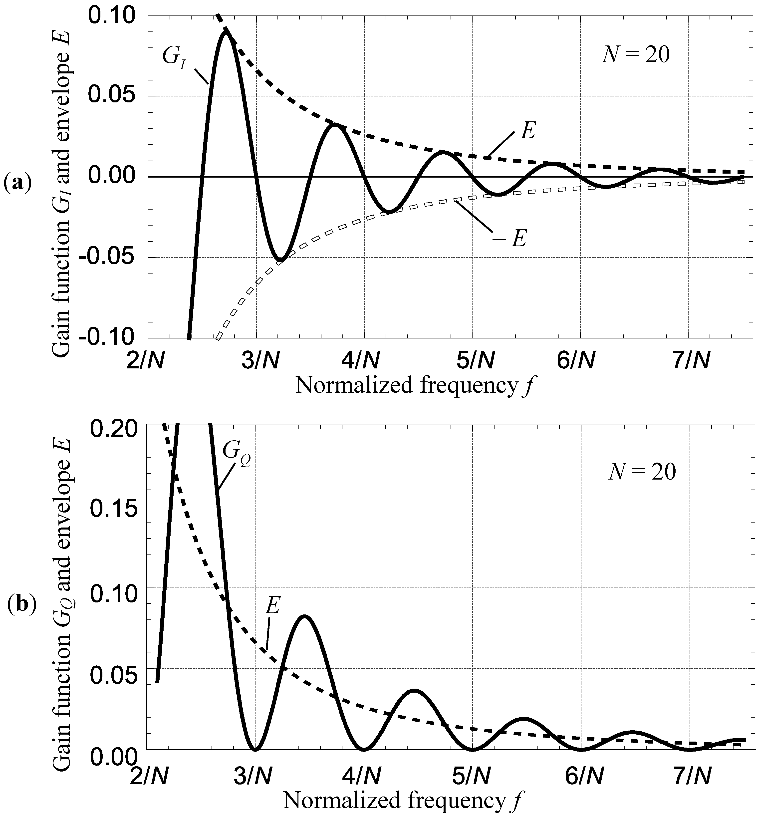
Within the frequency interval from 2/N to 1/2 both gains oscillate with a period of 1/N: the total number of oscillations for a given frequency interval is defined by N—the length of the sampled signal vector. In-phase gain crosses the x-axis at f = n/2N (where ǀnǀ ≥ 4 is an arbitrary integer of absolute value greater or equal 4). In contrast, the quadrature gain always stays positive and only touches x-axis at f = n/N (at every other in-phase crossing).
The envelope function is positive on this interval, monotonically falling and “compressing” the amplitude of the oscillating gains against the
x-axis. Within this frequency interval the suppression of the oscillations is mostly defined by the numerator in the envelope expression. So, the larger the number of samples
N, the greater the suppression. Hence for applications requiring DFT detector to operate in presence of significant DC offset
N has to be as high as practicable. To illustrate the behavior described above, the plots of both gains for
N = 20 are shown on
Figure 1.
Figure 1.
DC leakage gains of Equation (1) as functions of the normalized frequency f above f = 2/N: (a) in-phase component GI; and (b) quadrature component GQ.
Figure 1.
DC leakage gains of Equation (1) as functions of the normalized frequency f above f = 2/N: (a) in-phase component GI; and (b) quadrature component GQ.
It is worth noting that the “exponential-looking” decline is predominantly determined by the tangent function in the denominator of the envelope. The envelope function turns nearly linear with the slope inversely proportional to
N2 as it crosses
x-axis at the Nyquist frequency
f = 1/2 as both sine functions in the denominator are close to unity and:
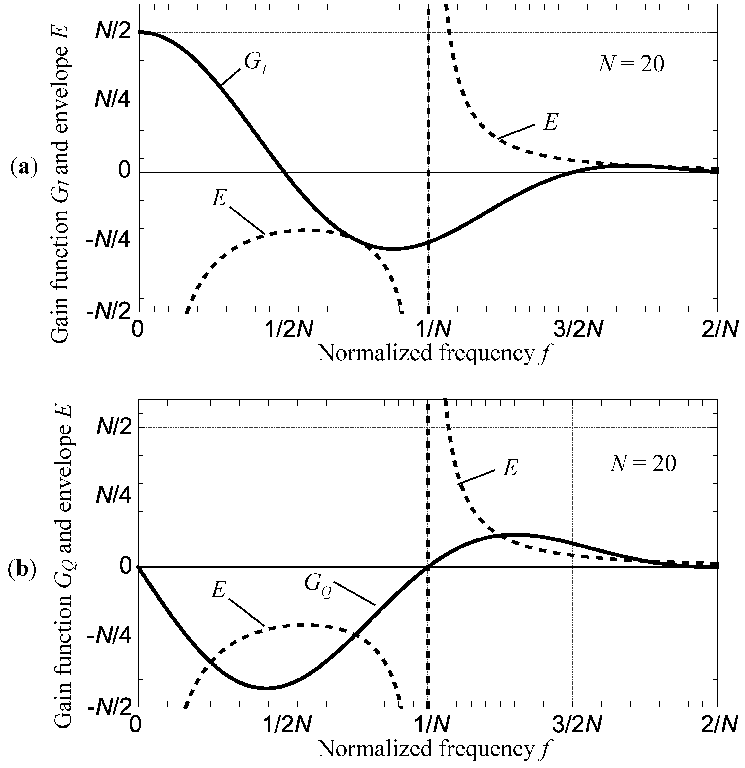
Within the frequency interval from 0 to 2/
N, however, the behavior of both gains change quite dramatically as the envelope function turns from suppression to amplification, see
Figure 2 generated for
N = 20. The larger the
N and the stronger the oscillations were suppressed above
f = 2/
N, the higher the amplification and the steeper the transitions produced by the envelope function below
f = 2/
N. As a result, the gains reach substantial magnitudes that are proportional to
N. The
y-axis is scaled and labeled in terms of
N to better illustrate this dependence.
Figure 2.
DC leakage gains of Equation (1) as functions of the normalized frequency f below f = 2/N: (a) in-phase component GI; and (b) quadrature component GQ.
Figure 2.
DC leakage gains of Equation (1) as functions of the normalized frequency f below f = 2/N: (a) in-phase component GI; and (b) quadrature component GQ.
Also, the envelope function is not monotonic on this interval—it suffers from two singularities at f = 0 and f = 1/N, where the denominator is 0: at the first point because = 0 and at the second point because = 0. This alters the gains’ periodic behavior observed earlier above f = 2/N. In-phase gain GI continues to swing above and below x-axis, but the envelope function singularities override the two zeroes at f = 0 and f = 1/N giving gain a finite non-zero value at these two points. In contrast, the quadrature gain GQ retains all its zeroes. Zeroes of the quadrature gain GQ are of higher order then the envelope singularities and the singularities are getting suppressed. Due to the sign change of the envelope function between the two singularities, the quadrature gain GQ now crosses x-axis instead of touching it and turns negative between f = 0 and f = 1/N.
Both gains feature rather large values within this frequency interval: in-phase gain GI reaches its maximum of N/2 at f = 0 and quadrature gain GI increases to a negative value of similar magnitude at a frequency a bit lower than f = 1/2N. This kind of gains behavior at low frequencies occurs because of the sampling interval becoming shorter than a single period of the test phasor and the distortion introduced by the window function.
At this point it is worth recalling the two oscillating multiplicands: Sin(2πfN) and 2Sin2(πfN) in the expressions for gains, which turn into 0 at 2πfN = πm and πfN = πn, or, solving for f yields f = m/2N and f = n/N respectively, where m and n are arbitrary integers. The singularities of the envelope function override the two zeroes at m = 0, ±2, so the frequencies at which the in-phase output SI (f) is not affected by DC leakage are f = m/2N, where m ≠ 0, ±2, but otherwise m is an arbitrary integer. The quadrature output SQ (f) is not affected by the DC leakage at f = n/N, where n is an arbitrary integer. Both outputs experience no DC leakage at f = n/N, where n ≠ 0, ±1, but otherwise n is an arbitrary integer. Evidently, no DC leakage occurs at the frequencies, where the test phasor is continuous.
The useful practical outcome of this analysis is that, in addition to frequencies at which the DFT achieves full suppression of the DC offset, this analysis identifies the frequency ranges where the DFT produces a rather substantial digital gain. The influence of the DC offset has to be taken into consideration or it can easily overwhelm the AC components in the signal of interest. On the other hand, this analysis shows that in addition to the conventional task of measuring AC signals, the DFT detector is capable of measuring DC signals. If a certain application requires measuring both AC and DC signals, the detector can easily switch between these tasks without any additional hardware dedicated to DC measurements.
Another useful practical outcome of this analysis is that it identifies the frequencies at which the DFT achieves full suppression of the DC offset for both in-phase and quadrature components and twice as many frequencies at which DC offset is fully suppressed for in-phase component only. For certain detector implementations when the AC input may contain an unknown DC offset, the latter could be discovered and measured by tuning the detector in and out of the frequencies of full DC suppression and observing the changes in both detector outputs.
3.2. Elimination of the AC Leakage from DFT Detector Output
A no-offset AC signal synchronized with the test phasor is usually represented as
, where
A and ϕ are the amplitude and phase of the signal respectively. At any
f the “ideal” detector is supposed to produce the outputs
Sx and
Sy proportional to
and
with the constant gain factor. In case of the single-frequency DFT detector, the in-phase and quadrature outputs of the detector can be expressed as:
and:
Both signals are directly proportional to the amplitude
A as expected of the ideal detector, but the dependence on phase ϕ is a bit more complicated. Through the trigonometric identity:
it is evident that the outputs
SI and
SQ are linear combinations of
and
:
and:
These two expressions can be written in a more compact the matrix form:
where
It immediately follows that
, so the earlier matrix expression can be written referencing only
a,
b and
d:
The explicit dependence of the matrix coefficients on f and N is omitted going forward for the sake of compactness. Now a can be considered an AC gain factor for the in-phase component, and coefficient d—AC gain factor for the quadrature component of the signal. Coefficient b can be thought of as a measure of an additive crosstalk or “leak” between the in-phase and quadrature channels of the detector. It follows then that for the DFT detector to perform ideally it is required that a = const, d = const and b = 0 for any frequency f. The behavior of these three coefficients as a function of f and N fully defines the performance of the DFT detector.
The same Hanning window is included in this analysis:
so:
and:
The closed forms for the all three sums above do exist and are found to be:
It is worth noting that a and d share the same constant baseline and their varying components as functions of f and N are the same, except they have the opposite sign.
It is easy to observe that these three coefficients contain functional arrangements analogous to those found in expressions for DC leakage gain factors explored earlier, except 2f replaces f in the arguments, so the AC leakage gains change twice as fast with respect to normalized frequency. Similar to the DC leakage, all three coefficients are periodic functions of f, only with the period of 1/2. Coefficients a and d are symmetric functions and b is an antisymmetric function of frequency. Also, within the first period the coefficients a and d are symmetric and b is antisymmetric with respect to f = 1/4 point—half the Nyquist frequency. Due to the aforementioned properties, consideration of the coefficients a, b and d as functions of frequency can be limited to the first half of the first period without any loss of generality.
A common subexpression, found in all three matrix elements
a,
b and
d, can be treated as an envelope function:
which defines the magnitude of the oscillating multiplicands:
Sin(4π
fN) and 2
Sin2(2π
fN). This allows for more compact expressions for the three matrix coefficients:
To illustrate the behavior of these three gains as a function of frequency, they are plotted at
N = 20 for the range above 1/
N, please see
Figure 3.
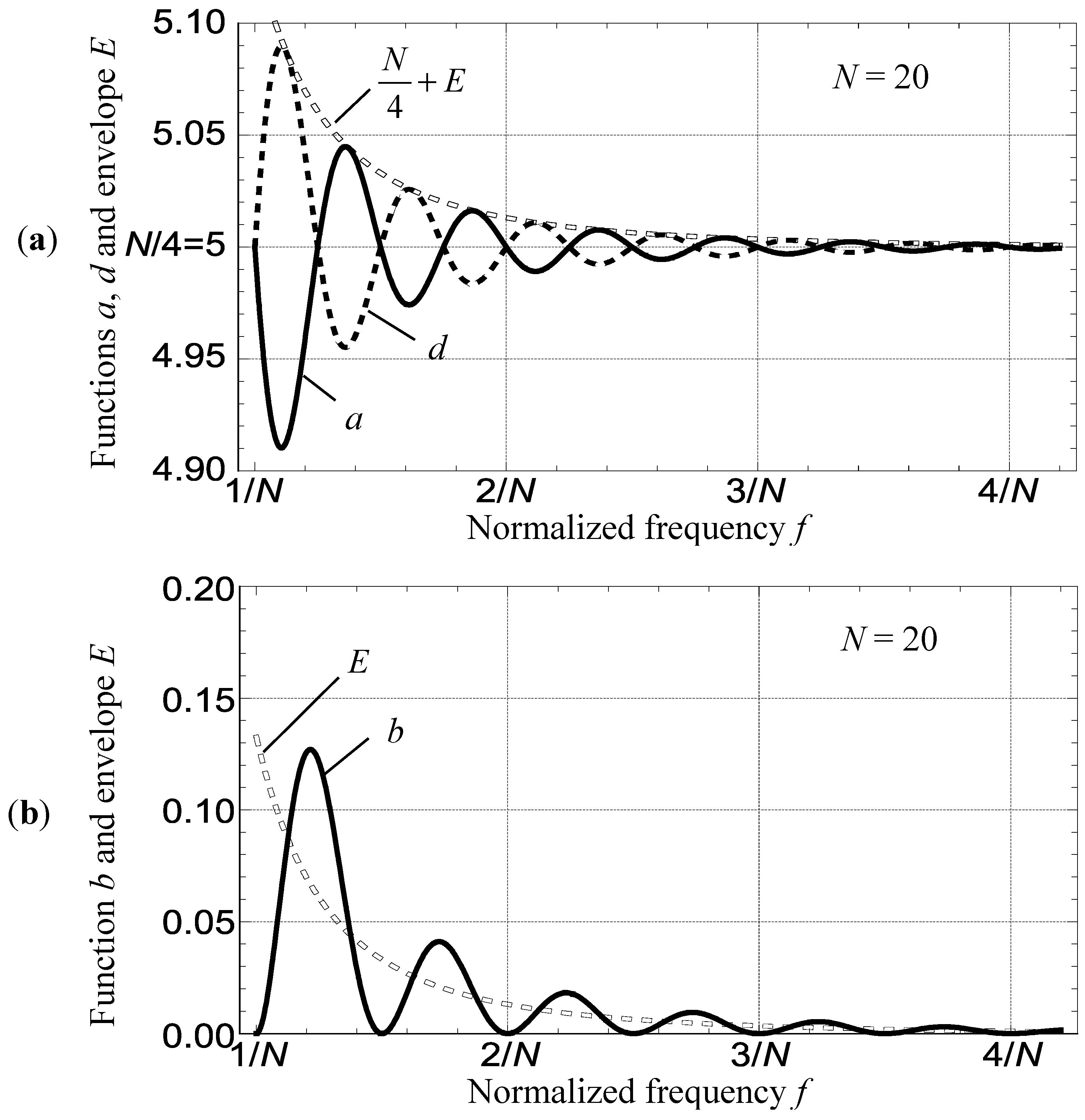
Figure 3.
AC leakage gains of Equation (2) as functions of the normalized frequency f above f = 1/N (a) matrix elements a and d and (b) matrix element b.
Figure 3.
AC leakage gains of Equation (2) as functions of the normalized frequency f above f = 1/N (a) matrix elements a and d and (b) matrix element b.
In contrast to the DC leakage, the gain coefficients a and d oscillate around the N/4 baseline instead of zero and the envelope function compresses these oscillations toward this baseline. The crosstalk coefficient b is always positive and only touches the x-axis.
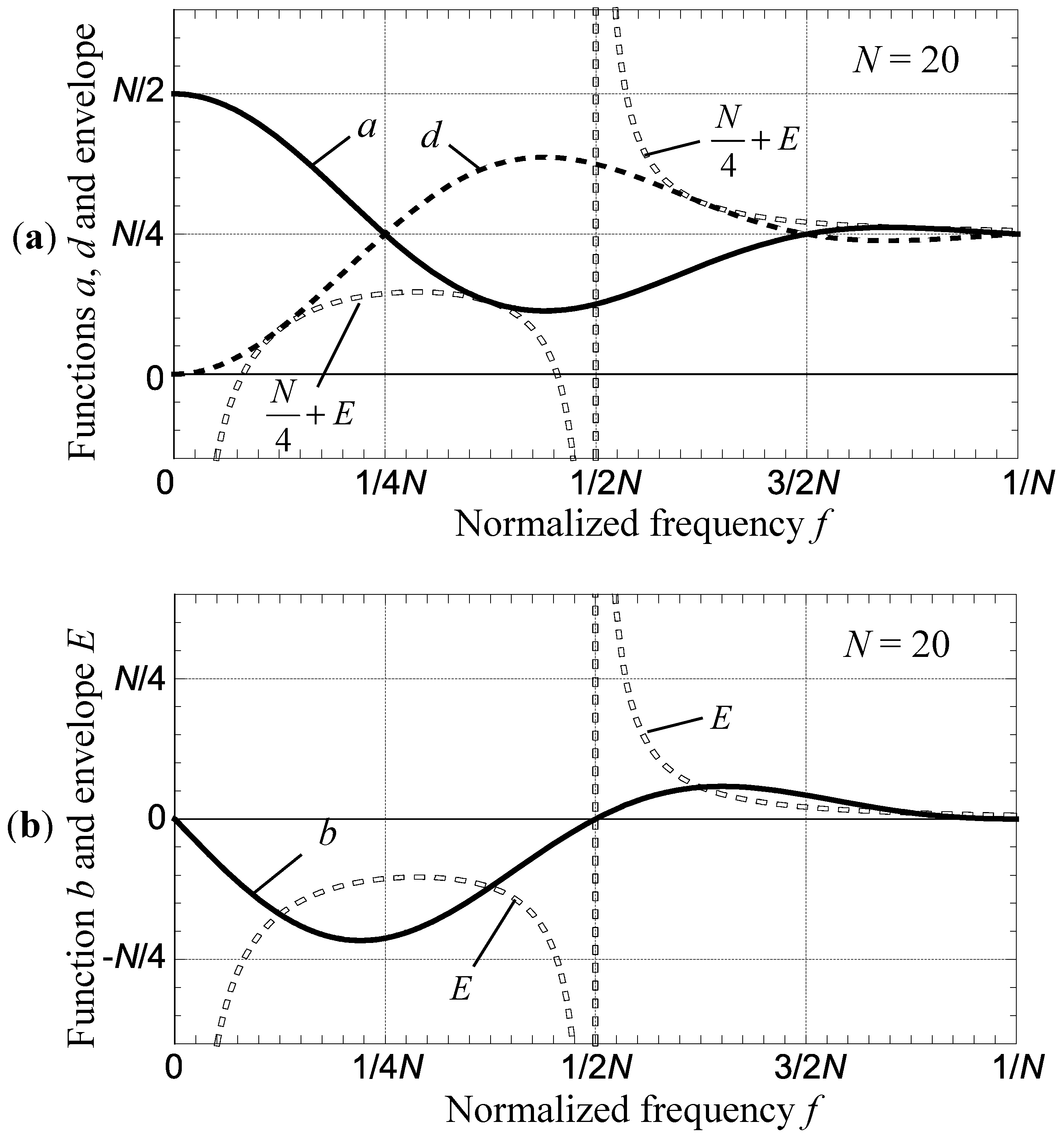
Within the frequency interval from 0 to 2/
N, however, the behavior of both gains change quite dramatically as the envelope function turns from suppression to amplification: see
Figure 4 generated for
N = 20. The larger the
N and the stronger the oscillations were suppressed above
f = 2/
N, the higher the amplification and the steeper the transitions produced by the envelope function below
f = 2/
N. As the result, the gains reach substantial magnitudes that are proportional to
N. The
y-axis is scaled and labeled in terms of
N to better illustrate this dependence.
Similar to DC leakage discussed earlier, within the frequency interval from 0 to 1/
N the behavior of all three coefficients change drastically as the envelope function turns from suppression to amplification. Also, the envelope function is not monotonic below
f = 1/
N as it suffers from two singularities at
f = 0 and
f = 1/2
N, where the denominator is 0: at the first point because of
Tan(2π
f) = 0 and at the second point because of
which changes the periodic behavior of the coefficients
a,
b and
d. Coefficients
a and
d continue to swing above and below their baseline of
N/4
x-axis, but the two baseline intersections at
f = 0 and
f = 1/2
N are overridden by the envelope singularities. In contrast, the crosstalk
b retains all of its zeroes, but crosses the
x-axis instead of touching it.
Figure 4.
AC leakage gains of Equation (2) as functions of the normalized frequency f below f = 1/N (a) matrix elements a and d and (b) matrix element b.
Figure 4.
AC leakage gains of Equation (2) as functions of the normalized frequency f below f = 1/N (a) matrix elements a and d and (b) matrix element b.
Similarly to the DC leakage, the larger the
N and the stronger the oscillations were suppressed above
f = 1/
N, the higher the amplification and the steeper the transitions produced by the envelope function below
f = 1/
N. As the result, the coefficients
a and
d deviate substantially from their
N/4 baseline and while
a doubles to
N/2
d falls down to 0 at
f = 0. The crosstalk
b crosses from positive to negative at
f = 1/2
N and bottoms out at substantial negative values at
f slightly less than 1/4
N and rises back to 0 at
f = 0. This behavior is illustrated on
Figure 4, generated for
N = 20. To better emphasize the aforementioned dependencies, the
y-axis is scaled and labeled in terms of
N.
All three coefficients feature rather significant deviations from their respective baselines. This kind of gains behavior at low frequencies is the direct result of the sampling interval being shorter than a single period of the test phasor and the input signal.
At this point it is worth recalling the two oscillating multiplicands:
and
, which turn into 0 at
and
. Solving for f yields f = m/4N and f = n/2N respectively, where m and n are arbitrary integers. The singularities of the envelope function override the two zeroes at m = 0, ±2 in the coefficients a and d, so the frequencies at which a and d contribute no AC leakage are f = m/4N, where m ≠ 0, ±2, but otherwise is an arbitrary integer. Coefficient b contributes no AC leakage at f = n/2N, where n is an arbitrary integer. All three coefficients contribute no AC leakage at f = n/2N, where n ≠ 0, ±1, but otherwise is an arbitrary integer. Evidently, no AC leakage of a synchronous AC signal occurs at the frequencies, where the test phasor is continuous, but it is also sufficient for a discontinuous test phasor to have an integer number of half-cycles for AC leakage to turn 0.
Also, recalling earlier discussion regarding the DC leakage that was found to turn 0 at f = n/N, where n ≠ 0, ±1, but otherwise n is an arbitrary integer. It is easy to see that every other point of zero AC leakage coincides with zero DC leakage, so no leakage at all takes place at f = n/N, where n ≠ 0, ±1, but otherwise n is an arbitrary integer.
The useful practical outcome of this analysis is that it uncovers the behavior of all three coefficients which can be relied upon at the detector or the whole system design stage. It also identifies the frequencies at which the crosstalk is fully suppressed (b = 0) while both a and d gains equal N/4.
The most useful practical outcome of this analysis is that it leads to the new method of processing the single-frequency DFT data described below that allows the achievement of zero leakage performance at any frequency within DFT detector operational range and resolution. With the analysis above, it is possible to calculate all three coefficients for any frequency
f and length of the input vector
N, and then for any measured values of
SI and
SQ to completely eliminate the AC leakage by simply solving the system of linear equations for
and
:
The denominator
is a “well-behaved” function of frequency, which turns zero only at the point f = 0, but is always negative at other frequencies. With f increasing, the denominator quickly falls to a −N2/16 baseline, exhibiting slight oscillations above it.
This approach eliminates all AC leakage errors and allows for accurate recovery of
and
from the measured values of
SI and
SQ not only when the measurement is performed over only a few cycles of the AC signal, but also over just a fraction of a single cycle. Publication [
27] proposes to divide system clock to stay away from significant leakage errors at frequencies below 1 KHz, while the proposed method allows the elimination of those errors at any frequency with the same system clock.
Application of this method achieves the maximum accuracy possible for a given DFT detector implementation. The remaining systematic accuracy-limiting factors are intrinsic to the detector digital design: truncation of the test phasor amplitude and phase, limited resolution of the digitized input, truncations in the DFT fixed-point arithmetic, etc.
Another useful practical outcome of the analysis given in this and the previous section is that it allows for easy identification and correction of the fixed-point arithmetic overflow that may occur depending on given implementation of the DFT and the magnitude of the input DC and AC signal. As any fixed-point implementation restricts the dynamic range of the operands involved in the DFT calculations due to the hardware-limited bitlength, the summations may result in overflow. With the developed knowledge of the DC and AC leakage as a function of normalized frequency it is straightforward to anticipate the overflow near the extrema of the in-phase and quadrature gains and correct for it.
3.3. Conclusion/Summary
Several scientific publications reviewed in
Section 2: “Background and Related Fields”, mention the systematic errors and difficulties utilizing DFT by following the standard calibration methods. These systematic errors have been historically attributed to spectral leakage in measurements based on DFT detection. Following the basic principles of the Fourier transform, the theoretical analysis presented in this section identifies two separate sources of these systematic errors resulting from the discontinuity of the test phasors. Close-form expressions quantifying error magnitudes as functions of normalized frequency and length of the sampled sequence are derived in this section.
Knowing the source and the behavior of these errors it becomes possible to outline new calibration methodology that eliminates these errors from the measurements. Application of the results from this theoretical analysis to data correction and examples of practical measurements with a DFT-based integrated circuit is discussed in the following sections.
4. Experimental Results and Discussion
4.1. DFT Detector Combined with DDS: Integrated Circuit Network Analyzer AD5933/5934
Probably the only known mass-produced single-chip implementation of a measurement system based on a DFT detector is the AD5933/5934 integrated circuit by Analog devices. According to the datasheet [
4], the AD5933 is an impedance converter system solution that combines a programmable direct digital synthesizer (DDS) with a sampling ADC, Hanning window, and a DFT detector that returns real and imaginary data-words at a fixed sampling frequency and pre-programmed test frequency. The AD5933 device is a nearly ideal platform for experimentation as it dramatically exhibits all the effects of the single-frequency DFT detector-based system described in the theoretical section.
Applications based on AD5933 can greatly benefit from the proposed methods as the calibration techniques described in the datasheet and widely replicated in the literature are often inadequate. Also, there is an interest in low-frequency applications of this integrated circuit for measuring bio-impedance, corrosion, fluid monitoring, structural health, water quality, and properties of loudspeakers, manifested in a number of publications mentioned earlier. The known solution to AD5933 low-frequency operation is based on dividing down the external clock frequency, which requires additional hardware. The proposed methods allow for significant expansion of the low end of the frequency range without any additional hardware.
4.2. Experimental Setup: AD5933 Evaluation Board
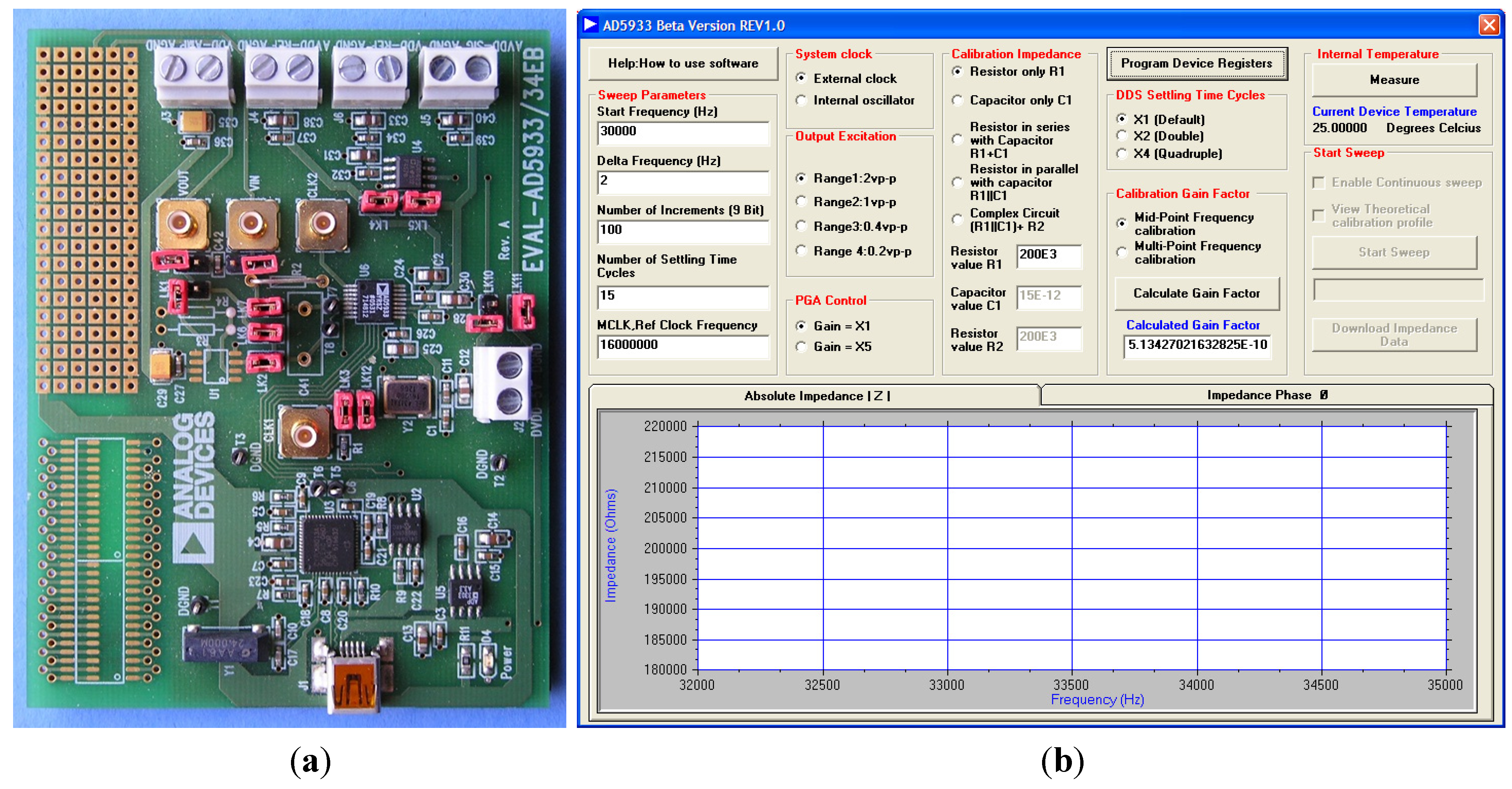
The only hardware utilized in this work was the commercially available AD5933 evaluation board by Analog Devices (
Figure 5a) and high-accuracy, calibrated resistors and capacitors. The evaluation board is supplied with the software (
Figure 5b) that allows the user to communicate with the AD5933 over the USB interface, setup and perform frequency sweeps and store the data from “Real” and “Imaginary” registers of the AD5933 as text files. The detailed description of the package including the board schematic, installation instructions, screenshots and a manual can be found in [
27].
The AD5933 is a complete single-chip network analyzer: it synthesizes its own excitation voltage, performs current defection, sampling, A-to-D conversion and DFT processing. As such, it is a closed system (a “black box”) that can be best characterized by using known calibrated impedances as DUTs and observing whether the digital output conforms to the response predicted by theory for a given DUT. Suitable calibration and data processing methods must be developed and applied to minimize or eliminate the observed discrepancies.
Figure 5.
Hardware and software utilized for data acquisition: (a) AD5933 evaluation board and (b) snapshot of the supporting software graphic user interface.
Figure 5.
Hardware and software utilized for data acquisition: (a) AD5933 evaluation board and (b) snapshot of the supporting software graphic user interface.
To bridge the gap between the theory discussed in previous sections and practical applications, it is necessary to provide values for the variables involved in the analysis. From the information in the datasheet [
4], the length of the sampled signal vector is 1024, so
N = 1024. From the block overview diagram of the AD5933 in the datasheet [
4] Figure 17 it follows that the direct digital synthesizer (DDS) of the device also provides synchronous cosine/sine test phasor to the DFT module, so it is necessary to connect the normalized frequency
f and the frequency control word for the synthesizer. In the datasheet [
4] the DDS frequency control word is also referred to as the
Frequency Code and this notation will be used for the remainder of this text.
The DDS is based on a 27-bit phase accumulator, which increments by the Frequency Code at every tick of the system clock; therefore, the frequency of the accumulator overflows is Frequency Code/227. Although not stated explicitly, from the text in the datasheet it follows that the sampling of the input (and also the test phasor) takes place every 4 accumulator increments. Then the current phase of the test phasor at a given summation index k is 2π∙(4∙Frequency Code/227)∙k plus some residual value from the accumulator previous overflow. Therefore, the normalized frequency f = 4∙Frequency Code/227 or f = Frequency Code/225.
As is typical for the digital systems such as DDS and DFT, all the considerations above are independent of the physical frequency. According to the datasheet, the accumulator increments every fourth cycle of the clock oscillator (internal or external) and thus the system physical frequency is (fClk/4)(Frequency Code/227) = fClk∙Frequency Code/229, where fClk is the clock oscillator frequency. In the interest of clarity, the experimental results are presented with the reference to the Frequency Code, as it is easy to convert back and forth between the latter and either the normalized frequency f or physical frequency based on the source of system clock.
4.3. Elimination of the DC Leakage from AD5933 Output Data
The characteristic feature of the AD5933 not explicitly mentioned in the datasheet [
4] is that the substantial DC offset is always present at the input of the DFT detector. The datasheet Figure 20 [
4] shows the “receive stage” of the device, depicting the VDD/2 voltage to be constantly present at the output of the amplifiers and at the input of the ADC in the absence of external circuits connected to pin 5 (VIN). Therefore, some binary number of a magnitude close to half of the ADC full scale is always present at the input of the DFT detector by design.
To observe the effect of this DC leakage experimentally it is sufficient to disconnect everything, except the feedback resistor, from the pin 5. This turns the internal amplifier circuit of the receiving stage into a voltage follower that passes VDD/2 to the ADC input. Then a sweep can be performed by programming the AD5933 with the parameters shown in
Table 1 (as referred to in the datasheet).
Table 1.
Sweep parameters.
Table 1.
Sweep parameters.
| Start Frequency Code | 350 |
| Frequency Increment Code | 150 |
| Number of Increments | 511 |
| Output Voltage Range | Any |
| Programmable Amplifier Gain | Any |
| External/Internal system clock | Any |
| Number of Settling Cycles Register D0-D8 | Any, except 0 |
| Number of Settling Cycles Register D9-D10 | 0 |
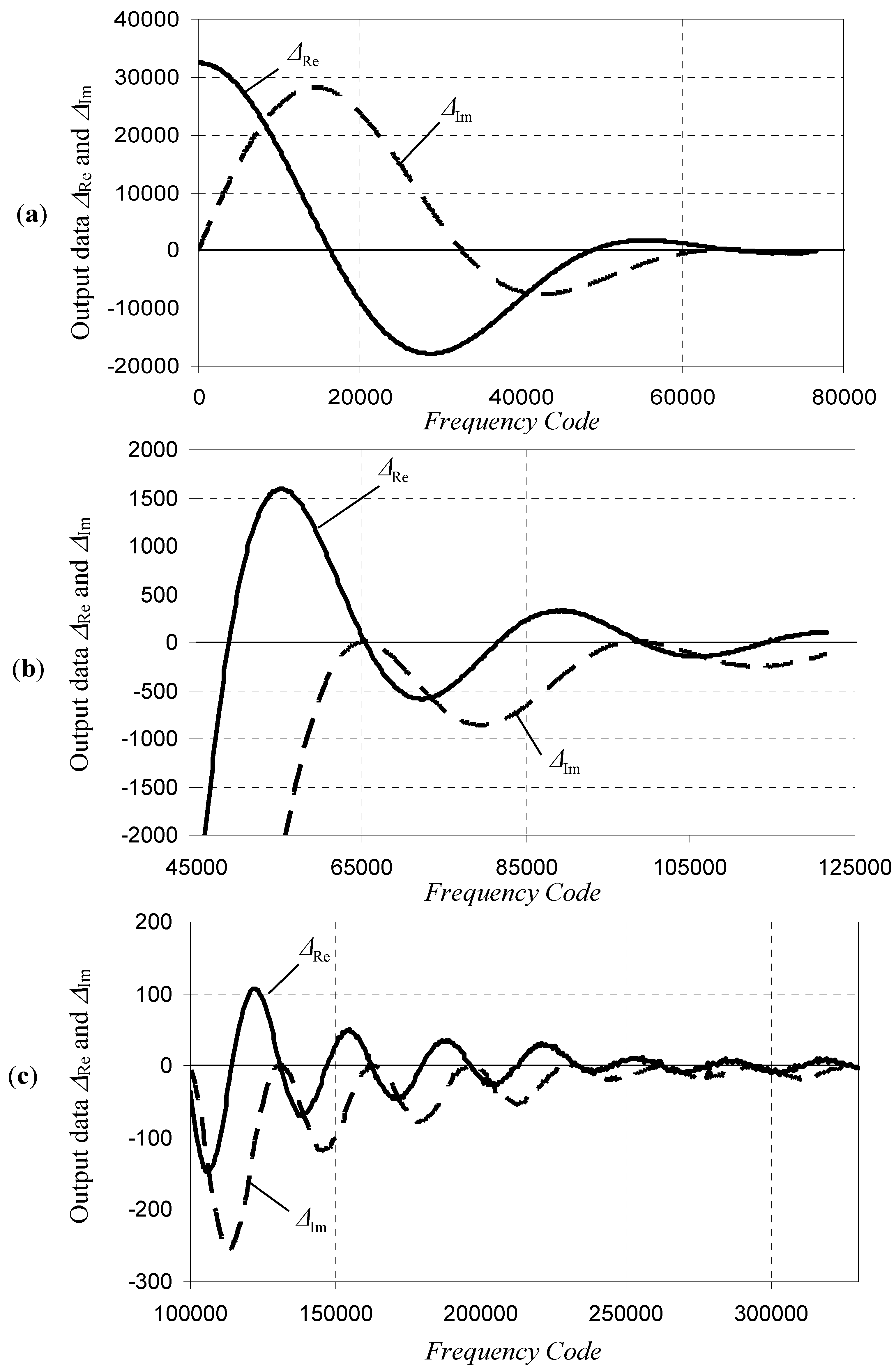
To distinguish experimental data from the correspondent identifiers SI and SQ in the theoretical section the internal DC leakage data collected from the AD5933 output registers is designated as ΔRe and ΔIm respectively.
The output data collected from the “Real” and “Imaginary” registers is plotted as a function of
Frequency Code and shown on
Figure 6a.
The “Real” and “Imaginary” data behave predominantly as predicted by the theory for Δ
I and Δ
Q and their respective gain factors in the range of
f from 0 to 2/
N (
Figure 2), except for the inversion of the imaginary data and some additional gain in both channels. The likely reason for the inversion is that the minus sign in front of the sum of samples of the test sine vector is implied, but not implemented in the device. A sweep with the same set of parameters except for Start Frequency Code = 45,000 produces the Δ
Re and Δ
Im data shown in
Figure 6b. Again, the data collected from the device behave as predicted by the theory for
SI and
SQ in the range of
f above 2/
N with the real data oscillating around zero and imaginary data only touching it. Sweeping further with the same parameters, except for higher Start Frequency Code = 100,000 and Frequency Increment Code = 450, it is easy to observe that the behavior predicted by the theory continues at higher frequencies, please see
Figure 6c.
Although decreasing in magnitude with increasing
Frequency Code, the DC leakages Δ
Re and Δ
Im still far exceed other sources of errors (irregular ripples barely visible on the chart
Figure 6c). Unless this effect of the DC leakage is taken into account and eliminated using the proposed method, the data from AD5933 contains a significant systematic error and the device cannot be utilized to its full potential.
To illustrate this matter in terms of physical frequency: with the external clock frequency of 16 MHz, the ranges covered in these three experiments and shown in
Figures 6a–c were approximately from 10 to 2299 Hz, from 1341 to 3626 Hz and from 2980 to 9833 Hz respectively. Publication [
27] states that at frequencies below 1 KHz the errors become very significant, but
Figure 6c indicates that those errors are still dominant at frequencies an order of magnitude higher than that.
The calibration method recommended in the datasheet aims to correct only for multiplicative gain and the resulting accuracy suffers greatly from this DC leakage systematic error, which is additive in nature. Narrowing the frequency range, assuming the gain linearly changing across the sweep and using multi-point calibration as advised do not help much, as the DC leakage error oscillates with the frequency.
Based on the information discussed above, the new calibration method has been developed. To remove the effects of the DC leakage the following steps have to be taken:
Disconnect any circuits except for the feedback resistor from pin 5 (VIN).
Take a sweep within the intended frequency range and store data in some kind of memory, in a microcontroller, host PC, etc.
Connect the circuit of interest to pin 5 and take a sweep.
Subtract the data recorded in step 2 from the data collected in step 3—the result is the response of the circuit of interest (which may or may not include contribution from its own DC offset).
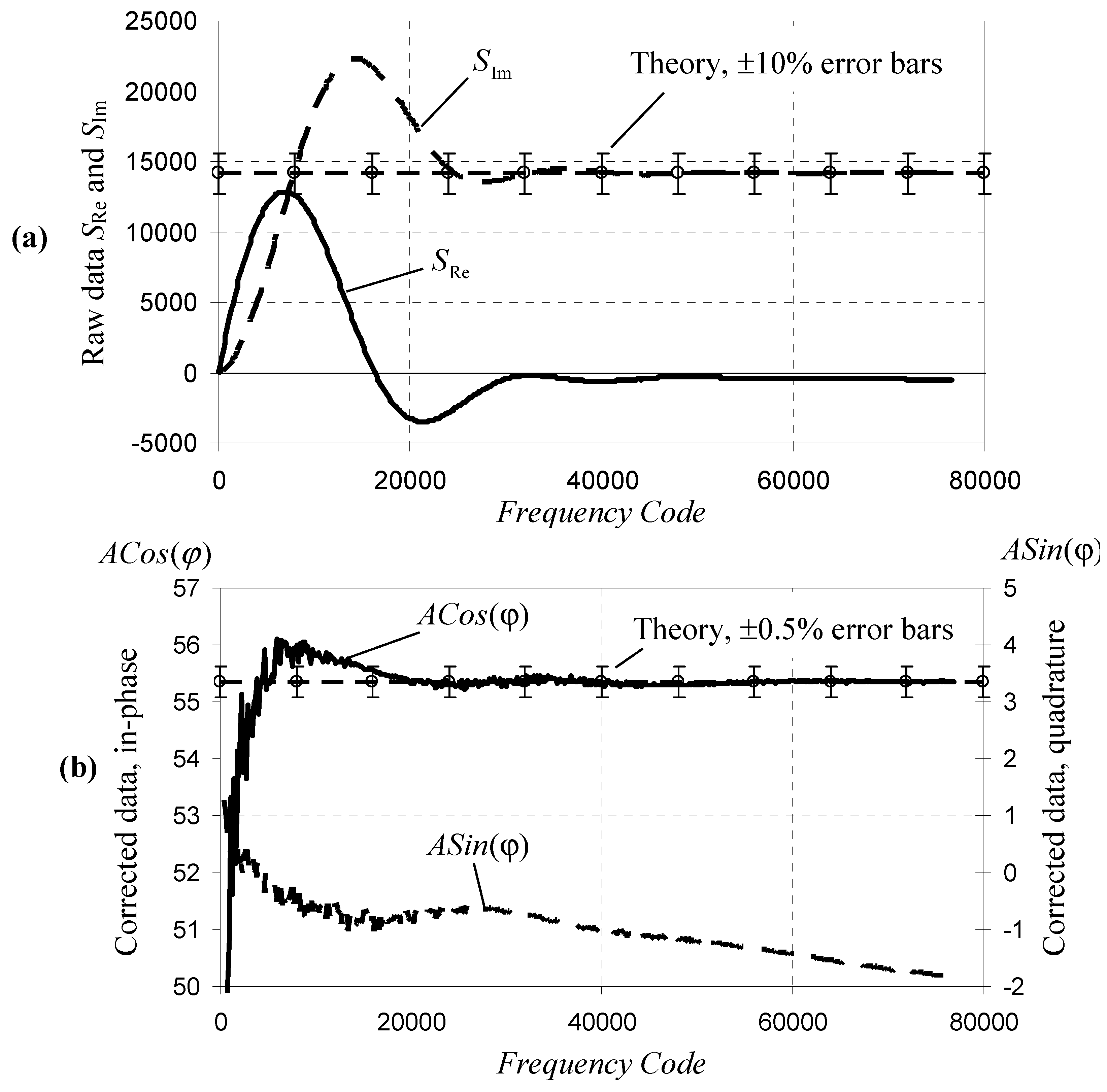
Figure 6.
Experimentally observed internal DC leakage ΔRe and ΔIm: data from the AD5933 “Real” and “Imaginary” output registers respectively, collected over 3 frequency ranges (a–c).
Figure 6.
Experimentally observed internal DC leakage ΔRe and ΔIm: data from the AD5933 “Real” and “Imaginary” output registers respectively, collected over 3 frequency ranges (a–c).
The above experiments can be easily reproduced at higher frequencies to observe that the error from the DC leakage decreases further, but still stays rather prominent in comparison to intrinsic system inaccuracies, noise and interference at all frequencies within the advertised operating frequency range.
The additional benefit of this method is that, due to additive nature of the DFT, other errors that are stable in time will all be subtracted from the signal of interest.
The software for calibration and data acquisition supplied with the AD5933 evaluation boards does not provide the functionality that could support the proposed procedure. The early version (rev. 1.0) of the software maps the contents of the “Real” and “Imaginary” registers to 16-bit signed integers [
27] and allows the user to save this data as text files, which can be used to implement the proposed method utilizing some external means.
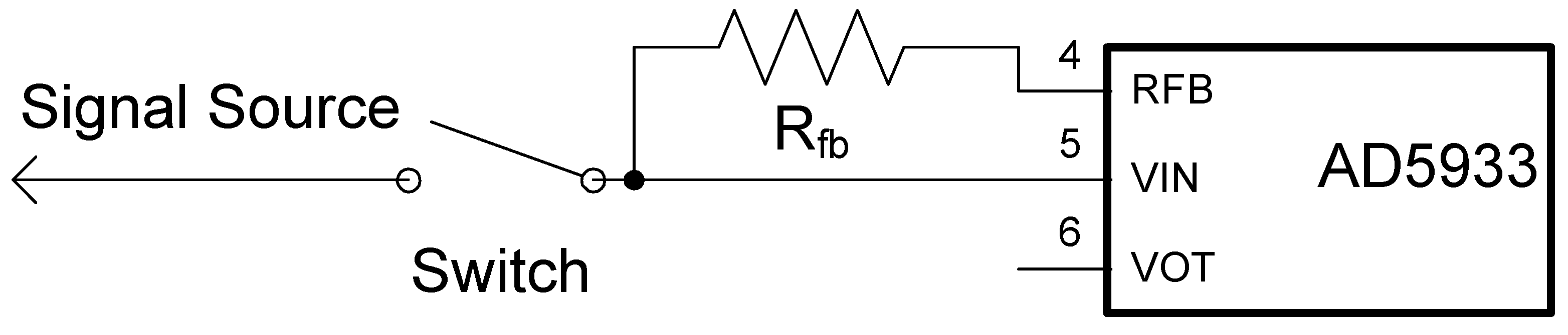
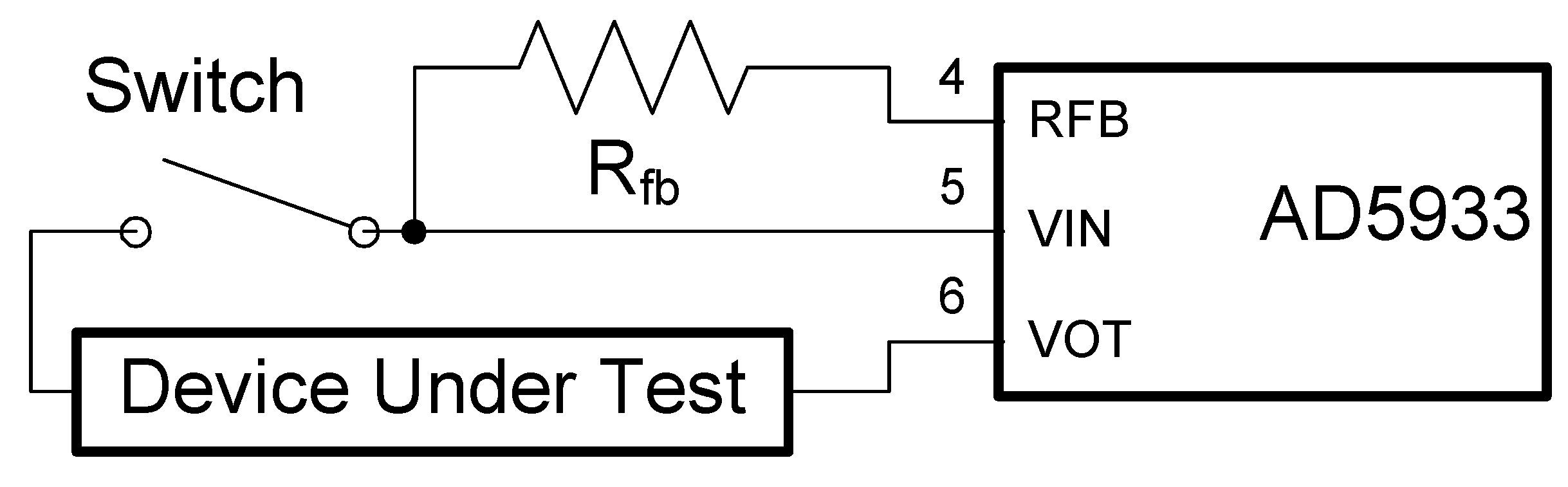
A simplified schematic for performing the proposed procedure for the network analysis—the intended purpose of AD5933—is illustrated in
Figure 7. The network is shown as the two-port Device Under Test (DUT). The DUT is not necessarily limited to a two-port circuit such as some passive impedance network, but could also represent a more complex multi-port network, for example, a filter, or an active circuit such as an audio amplifier or an active filter, analog front end (AFE) circuit,
etc.The switch is shown in open position for acquisition and recording of the DC leakage sweep to be subtracted from the following measurements of the DUT response to the AC excitation voltage from pin 6 (VOUT) when the switch is closed. The switch can also be replaced by a relay, analog semiconductor switch, and any other such means to provide the necessary switching function for temporary isolating the VIN node.
Figure 7.
Simplified schematic for eliminating AD5933 internal DC leakage from network analysis: internal DC offset is processed by the on-chip circuitry and recorded when the switch is open.
Figure 7.
Simplified schematic for eliminating AD5933 internal DC leakage from network analysis: internal DC offset is processed by the on-chip circuitry and recorded when the switch is open.
Depending on the specific nature of the DUT, it may also transfer some or all of the DC component of the excitation voltage from pin 6 (VOUT) to VIN node, so care must be taken to block this DC. A passable, but an inferior alternative would be to include it in the DC leakage calibration process at a cost of reducing the ADC dynamic range available for AC measurements.
Similarly, a simplified schematic for performing the proposed procedure for measuring the external signal is illustrated on
Figure 8. The switch is shown in open position for acquisition and recording of the DC leakage sweep to be subtracted from the following measurements of the signal of interest. Depending on the application, the excitation voltage from pin 6 (VOUT) may or may not be utilized for synchronization of the external signal source.
Figure 8.
Simplified schematic for eliminating AD5933 internal DC leakage from AC signal: internal DC offset is processed by the on-chip circuitry and recorded when the switch is open.
Figure 8.
Simplified schematic for eliminating AD5933 internal DC leakage from AC signal: internal DC offset is processed by the on-chip circuitry and recorded when the switch is open.
If the circuit of interest produces no DC offset of its own, the calibration method from the datasheet can now be applied and the calculations of the AC impedance based on the calibrated gain factor will yield much more accurate results.
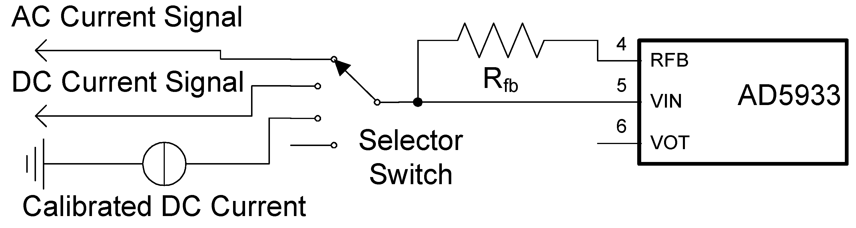
4.4. Measuring DC Signals with the AD5933
The theoretical analysis and subsequent experiments identified the frequency ranges, where the DFT detector produces substantial gains for DC leakage, both in real and imaginary data. A single frequency measurement within this range is sufficient to obtain the accurate value of a DC signal.
A simplified schematic for performing the proposed procedure is shown in
Figure 9. For illustration purposes let us assume that a user prefers to measure the DC signal utilizing the data from Imaginary data register. Looking at
Figure 2 and
Figure 6a it is easy to see that the DC leakage gain reaches maximum around
f ≈ 1.3/
N, which corresponds to
Frequency Code range of about 42450 to 42900 (1265 to 1279 Hz at 16 MHz clock).
Figure 9.
Simplified schematic for AD5933 calibration, DC and AC measurements: internal DC offset is processed by the on-chip circuitry and recorded when the selector switch is at the bottom, system DC gain is measured when the switch is connected to a calibrated DC current source. The same system measures AC current when the selector switch is in top position.
The procedure is as follows:
- (1)
Disconnect the input VIN node (selector bottom position).
- (2)
Program the Frequency Code into AD5934, and initiate the single-frequency measurement, read the content of the imaginary data register and store it.
- (3)
Connect VIN node to calibrated DC source, initiate the single-frequency measurement, read the content of the imaginary data register, subtract the value stored in step 2 value, calculate the ratio of the found difference to the calibrated DC source magnitude and store it—this is the system gain for DC signals.
- (4)
Switch to connect to the unknown DC signal, initiate the single-frequency measurement, read the content of the imaginary data register, subtract the value stored in step 2 value, divide by the system gain from step 3—the result is the unknown DC signal.
Equivalently, this method can be practiced with the real register data at frequency codes that correspond to acceptable gain values. Using data at a single frequency point from a single data register constitutes a minimalistic version of the proposed method, but the data from one or both real and imaginary registers at a single frequency or multiple frequencies, or data from a whole frequency sweep within suitable range, can be utilized to arrive at the DC signal value. While these versions of the proposed method may provide somewhat better statistics, additional measurement time and processing may prove to produce diminishing returns and have to be tailored to the application-specific requirements.
Obviously, the methods and the schematics in
Figure 7,
Figure 8 and
Figure 9 can be combined for switching AD5933 between measuring DC leakage, calibration, using the same DDS and DFT hardware for measuring DC and AC signals and performing the functions of network analysis. The method of removing the AC leakage from the AC signal measurements is discussed in the following sections.
4.5. Elimination of the AC Leakage from AD5933 Output Data
Since it has been discovered in the DC experiments that the practical implementation of the DFT in AD5933 inverts the sign of the inner product of the sampled input and the sine test vector, it makes sense to designate the data produced by the AD5933 as
SRe and
SIm to distinguish these from the correspondent identifiers in the theoretical section:
where
b and
d in the bottom row now change signs to account for the minus sign missing in the AD5933 DFT implementation.
Also, in AD5933, the DFT results are held in the 16-bit “Real” and “Imaginary” registers, which can hold values between 0 and 2
16 − 1 only and, as it was mentioned in the theoretical section, may overflow. The datasheet does not mention any hardware status flags indicating this condition and the software provided with the evaluation board [
27] offers no means of detecting and correcting the overflow. Luckily, the proposed method allows for easy overflow identification and correction by comparing the sign of the collected data to the one predicted by theory. In the experiments below, when the overflow occurs, the sign of the overflown data turns negative—the opposite of what is predicted by the theory—and such data can be corrected by simply adding 2
16 to it.
To experimentally observe the effects of DFT low-frequency behavior discussed in the theoretical section, after recording the DC leakage sweep with the feedback resistor
Rfb of 200 kΩ as explainedin the previous section (please see
Figure 7,
Figure 8 and
Figure 9), a test resistor of 140 kΩ is connected between pin 6 (VOUT) and pin 5 (VIN) (in place of the DUT in
Figure 7) through an additional circuit, ensuring that no DC current is flowing across the test resistor. The test sweep is performed with the settings same or similar to the ones used in the DC leakage section: please see
Table 2.
Table 2.
Sweep parameters.
Table 2.
Sweep parameters.
| Start Frequency Code | 350 |
| Frequency Increment Code | 150 |
| Number of Increments | 511 |
| Output Voltage Range | 2 V |
| Programmable Amplifier Gain | 1 |
| External/Internal system clock | Any |
| Number of Settling Cycles Register D0-D8 | 1 |
| Number of Settling Cycles Register D9-D10 | 0 |
The output data “Re” and “Im” collected from the “Real” and “Imaginary” registers is corrected for the fixed-point overflow and the DC leakage sweep recorded earlier Δ
Re and Δ
Im is also subtracted. The resulting data
SRe = Re − Δ
Re and
SIm = Im − Δ
Im is plotted on
Figure 10a.
Figure 10.
Raw data for 140 kΩ resistor as DUT: (a): raw data SRe and SIm and (b): data processed according to Equations (3) left y-axis for and right y-axis for . Systematic errors of several tens percent are reduced by processing to below 1% for most of the frequency range.
Figure 10.
Raw data for 140 kΩ resistor as DUT: (a): raw data SRe and SIm and (b): data processed according to Equations (3) left y-axis for and right y-axis for . Systematic errors of several tens percent are reduced by processing to below 1% for most of the frequency range.
The resistor produces no phase shift with respect to the excitation voltage, so ϕ = 0, therefore:
the “Real” and “Imaginary” data are proportional to the amplitude of the AC current
A and frequency-wise they should behave as the coefficients
a and −
b respectively. Instead, per
Figure 10a, the response appears as −
b and
d.
The reason for this is that, to the contrary of the textbook conventions and popular belief [
37,
45], the AC excitation voltage function generated by AD5933 with respect to the test phasor is sine and not the cosine. The current delivered by the resistor under test to VIN node is not the conventional
, but rather
. Therefore, according to the co-function identity:
the phase
in the expressions for
and
has to be substituted with
:
with a resistor under test, ϕ = 0, so:
which is the result observed experimentally.
For the convenience of obtaining the DFT results from AD5933 in the textbook form, further re-arrangement of the matrix coefficients from the theoretical section needs to be performed. As the AD5933 excitation function is sine, the input signal to the DFT is:
and also the minus sign in front of the sums in the expression for
is not implemented:
The resulting matrix coefficients are the following:
Solving the system of linear equations for
and
yields the following:
To process the experimental data shown on
Figure 10a, it is necessary to calculate the three matrix coefficients
a,
b and
d by substituting
N with 1024 and
f with 4∙
Frequency Code/2
27 in the expressions (2). It is worth noting that for a given
Frequency Code the envelope function needs to be calculated once as it is shared by all there coefficients and the term
is also shared by
a and
d. If multiple sweeps are to be performed over a given set of frequencies the coefficients
a,
b and
d can be calculated once and stored for processing of the incoming raw data.
This experimental data corrected for leakage is shown on
Figure 10b. The
y-axis for the in-phase component of the signal
is on the left and the
y-axis for the quadrature component
is on the right—both
y-axes are of the same scale, but of different origins to better show the transitions.
The frequency response of an ideal resistor measured by an ideal network analyzer is supposed to consist of a frequency-independent in-phase component and a zero quadrature component.
Figure 10a shows the raw data and, for illustration, a theoretical response of a resistor with ±10% error bars. It is easy to see that both in phase and quadrature data
SRe and
SIm deviate from the expected theoretical behavior by many tens of percent, especially at low frequencies.
Figure 10 (
b) shows the data processed according to Equations (3) and, for illustration, the theoretical response of a resistor with ±0.5% error bars, which is the system accuracy value found in the AD5933 datasheet [
4].
It can be seen that after the processing the in-phase component is much larger than the quadrature one and predominantly constant with the frequency at
Frequency Code above about 4000, decreasing sharply at lower
Frequency Code values. This means that the applied method allows for complete correction of the DFT leakage errors. Below
Frequency Code = 4000, which corresponds to about 120 Hz at 16 MHz clock, the inaccuracy of digital implementation of the DFT becomes prevalent. The quadrature component is close to 0, slowly decreasing into negative values with the increasing frequency. This behavior of the quadrature component results from the phase delay caused by the low-pass filter in front of the ADC, shown on the functional block diagram in the datasheet [
4]. This can be easily accounted for and further corrected by applying conventional textbook calibration techniques.
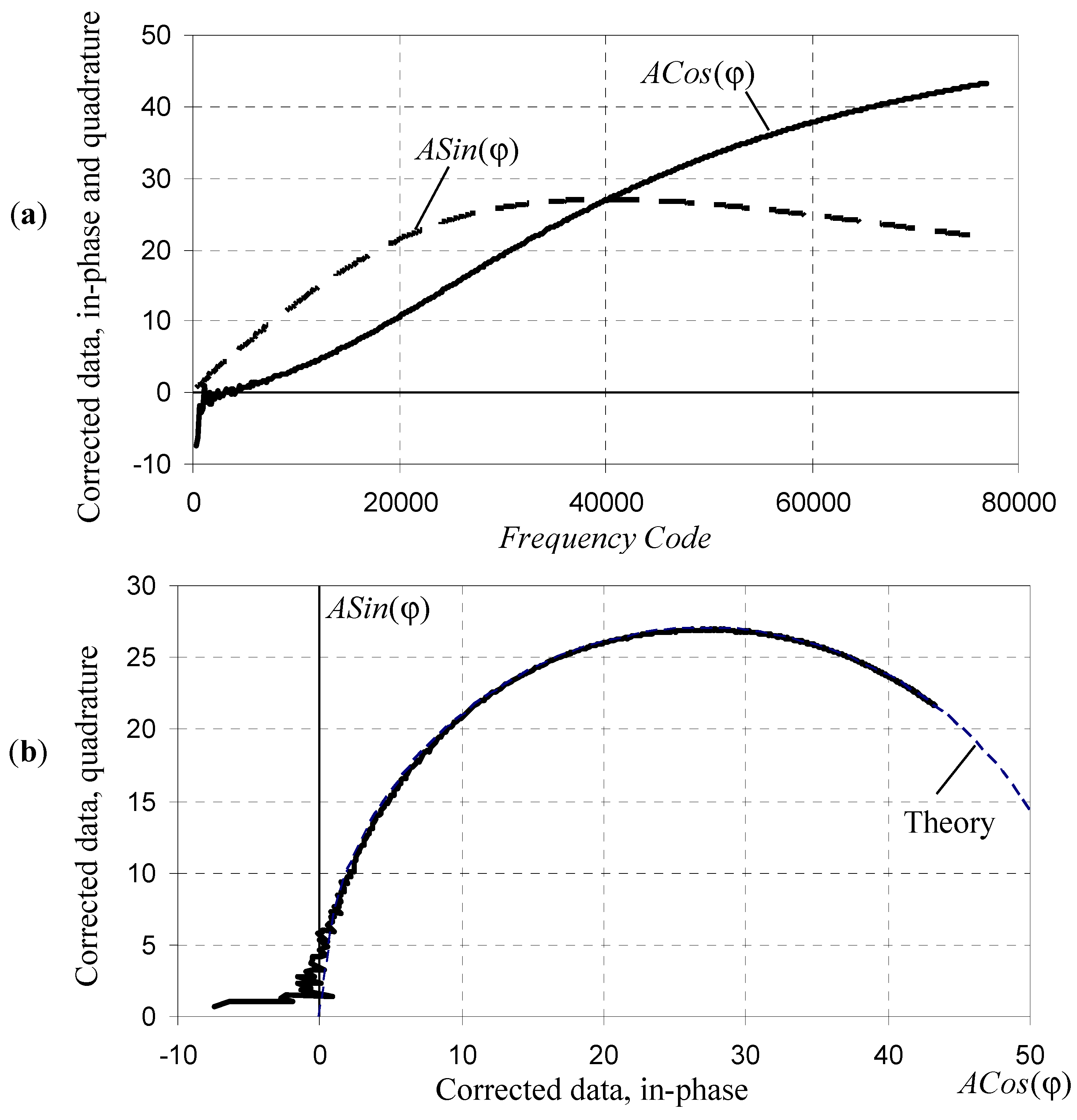
One more experiment demonstrating the ability of the proposed method to correctly recover both the in-phase and quadrature components is performed under the same settings as the previous one, except that the same test resistor of 140 kΩ is now connected in sequence with a 1nF capacitor. This type of impedance—a sequential RC network—is often observed in applications such as bioimpedance measurements, monitoring of corrosion, evaluation of protective coatings, electrochemical experiments, etc., requiring a wide frequency sweep in the low frequency ranges.
The register “Number of Settling Cycles Register D0-D8” value is set to 100 to let possible transient charges in the capacitor to dissipate prior to data acquisition. The output data collected from the “Real” and “Imaginary” data registers was again corrected for the fixed-point overflow and the DC sweep recorded earlier was subtracted. The resulting data processed according to the formulae above is shown on
Figure 11.
The in-phase and quadrature components are plotted as a function of
Frequency Code (
Figure 11a). These components are also plotted on a complex plane with the in-phase data plotted as the
x-axis values and the quadrature data as the
y-axis values (
Figure 11b).
Figure 11.
“Real” and “Imaginary” data for 140 kΩ resistor and 1nF capacitor sequential RC network collected by AD5933, processed according to Equations (3) and plotted: (a) as functions of frequency, and (b) on a complex plane: quadrature response ASin(ϕ) as a function of in-phase response ACos(ϕ).
The resulting chart accurately follows the arc—the expected theoretical response from ideal RC sequential network, except for the frequency codes below about 4000 (~120 Hz at 16 MHz clock), where the truncations and other errors inherent in the device’s digital implementation start appearing. The most significant contributing sources of these errors are: truncation of the phase and amplitude in the DDS, limited resolution of the sampling ADC, and truncations in the fixed-point arithmetic DFT core. Further reduction of the remaining systematic errors would require re-designing the chip and implementing higher-resolution binary representations of numbers and functions, which would lead to increasing bit width in look-up tables, arithmetic operations, resolution of DDS DAC, and sampling ADC, and likely result in higher power consumption and device cost.
After the additive DC leakage and the AC leakage errors have been eliminated from the raw data by this method, the conventional single-frequency-point calibration and multi-point calibration techniques can be applied and will produce accurate results over a much wider frequency range than when applied to raw data directly. The experimental data indicates that without any additional hardware the proposed method allows the expansion of the usable operational frequency range down to 100 Hz, enabling a verycost-efficient access to the frequencies two decades below 10 KHz. In the range above 10–20 KHz the DC and AC leakage errors do decrease and for certain low-dynamic range and narrow-frequency applications the AD5933 may deliver adequate results, but the proposed method enables a far superior performance at all frequencies, pushing the accuracy to the to the maximum that can be achieved by the device.


