1. Introduction
The natural space radiation environment is complex, containing high-energy photons, protons, neutrons, electrons, and heavy ions. Energetic heavy ions introduce transient, dense charge filaments along their path through an electronic device that can trigger catastrophic failure mechanisms and total ionizing dose degradation. The concentrations and types of ions vary significantly with altitude and inclination of angle of an orbit, recent solar activity, and the amount of protective shielding. These variations make it difficult to specify a typical space environment. Most particles found in the space radiation environment of the earth can be classified as: (1) trapped particles in the magnetic field of the earth—primarily protons and electrons; and (2) cosmic rays—heavy ions or protons of solar or galactic origin.
Power metal-oxide semiconductor-field-effect transistors (MOSFETs) have dominated the power device market since the 1980s and are found in most power supplies, DC-DC converters, and low voltage controllers. They are frequently selected for use in space-borne electronic systems. However, power MOSFETs, in the space environment, are susceptible to parametric degradation and to at least two catastrophic failure mechanisms that can be initiated by the passage of a single heavy ion through sensitive regions of the device structure. These failures are referred to as single-event burnout (SEB) or single-event gate rupture (SEGR).
Currently, the silicon trench (or UMOS) power MOSFET device design is supplanting the older vertical double-diffused power MOSFET (VDMOS) device design for many applications including low voltage switches. The radiation susceptibilities of the VDMOS technology have been studied and reported on extensively. However, at this time, there is much less data and analysis of heavy-ion degradation and/or failure of UMOS devices. Three mechanisms for heavy-ion degradation and/or failure due to heavy ion exposure have been reported for UMOS power transistors: (1) microdose; (2) single-event burnout (SEB); and (3) single-event gate rupture (SEGR).
This paper will summarize the state of knowledge on the degradation and/or failure of silicon trench (or UMOS) power transistors due to heavy-ion exposure (or energetic proton environments) such as encountered in spacecraft. The evolution of power MOSFET technology will be recounted and the current physical understanding of the interaction between heavy-ion radiation and the UMOS device technology as it applies to the three mechanisms above will be described. Designers of spaceborne power electronics systems that incorporate UMOS power MOSFET technology need this information in order to evaluate the survivability of their designs.
2. Evolution of Power MOSFET Technology
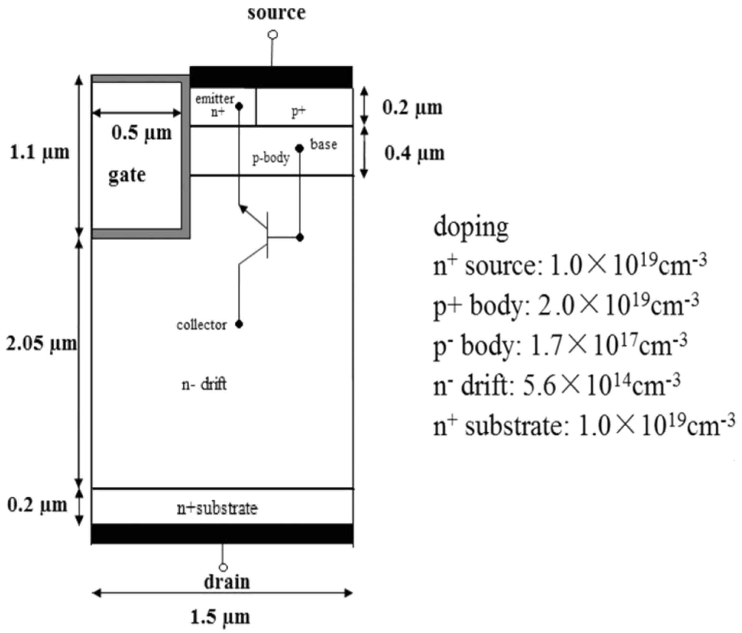
Several power MOSFET device designs had been explored by the early 1980s. In that time period, the Vertical Double-Diffused MOS structure (VDMOS or simply DMOS) [
1] as illustrated in
Figure 1 emerged as the dominant MOS power device technology. The first generation of macrocell VDMOS power transistors was introduced into the commercial market by International Rectifier. Generally, power MOSFET design and process technology has followed the evolution of CMOS technology following the leading edge with a time delay of three-to-five years.
In the 1990s, power MOSFET device design based on trench technology became feasible and held several advantages when compared to VDMOS [
2,
3]. The trench or UMOS transistors delivered an improved switching resistance (R
DSON) and reduced gate charge when designed for products with a drain voltage capability lower than 100V. The silicon trench power MOSFET is the leading low-voltage technology in the market today and is offered by a number of commercial, power MOSFET suppliers.
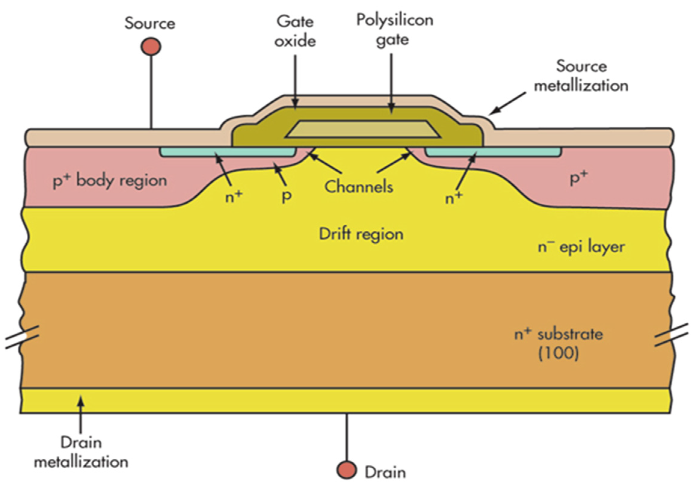
UMOS power transistors are fabricated with trenches etched into the silicon; gate oxides are then grown along the trench sidewalls; and then the trenches are filled with polysilicon, which is the gate material. Incorporating a trench structure significantly increases the channel width when compared to the VDMOS power transistor, and also eliminates the JFET region (commonly referred to as the neck region in the vertical power MOSFET). In some trench technologies, a thicker oxide is used at the trench bottom to dramatically reduce the capacitance between the gate and drain and to enhance device switching performance.
Figure 1.
Schematic cross-section of an n-channel vertical power MOSFET. After ref. [
1].
Figure 1.
Schematic cross-section of an n-channel vertical power MOSFET. After ref. [
1].
A cross-section of an n-channel UMOS power MOSFET showing typical device structure is given in
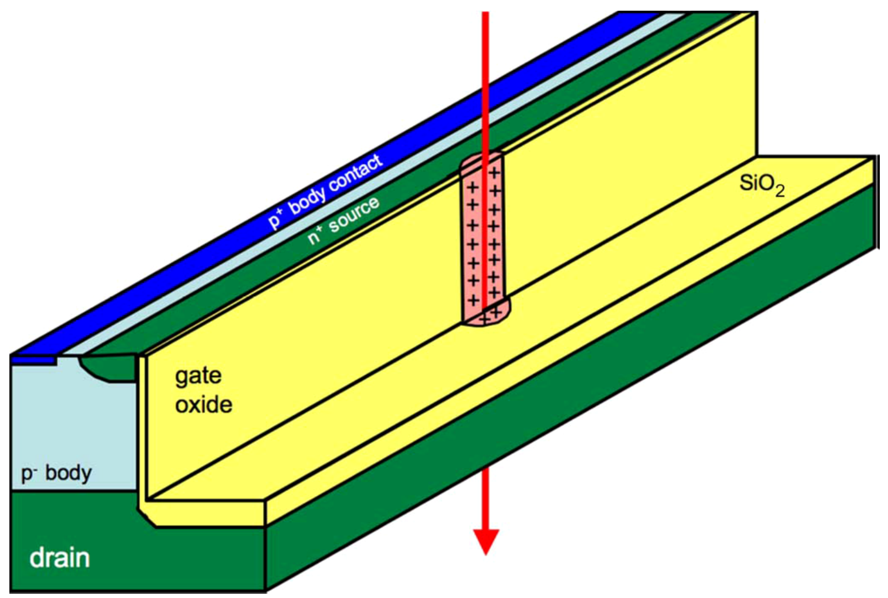
Figure 2. Contact to the drain is made on the bottom surface of the silicon chip. The rather thick n-type epitaxial drain region (drift region) is required to drop the large drain to source voltages that the power transistor must block while operating in the OFF state. Typically, many cells (often laid out as stripes) are connected in parallel to effectively create a very wide channel (while retaining the channel length of the individual cell) to achieve the large currents required in the ON state. When turned ON, the channel forms and current flows from the source through the channel to the drain. Note the parasitic npn bipolar-junction-transistor (BJT) inherent to the structure. The source, body, and drain regions of the MOSFET comprise the emitter, base, and collector regions of the parasitic BJT. During normal operation, this parasitic BJT is always turned off due to the common source-body metallization that shorts out the base-emitter junction.
Figure 2.
Schematic cross-section illustrating the structure of an n-channel UMOS MOSFET. After ref. [
4].
Figure 2.
Schematic cross-section illustrating the structure of an n-channel UMOS MOSFET. After ref. [
4].
3. Microdose Effects in UMOS Technology
In 2008, S. Liu
et al. [
5] published a detailed analysis of total ionizing dose test results on commercial UMOS power MOSFETs illustrating that these devices have similar responses as radiation hardened VDMOS power devices but with, in general, larger parameter shifts. These tests were done with Co
60 gamma rays. The changes are attributable to trapped charge in the gate oxide [
6]. Liu
et al. note that a radiation hardened gate oxide would mitigate most of the observed total dose effects observed.
However, ionizing radiation total dose effects from heavy ions and protons yield very different results when compared to Co
60 tests. Felix
et al. [
7] reported enhanced degradation and microdose effects in UMOS power devices in 2007.
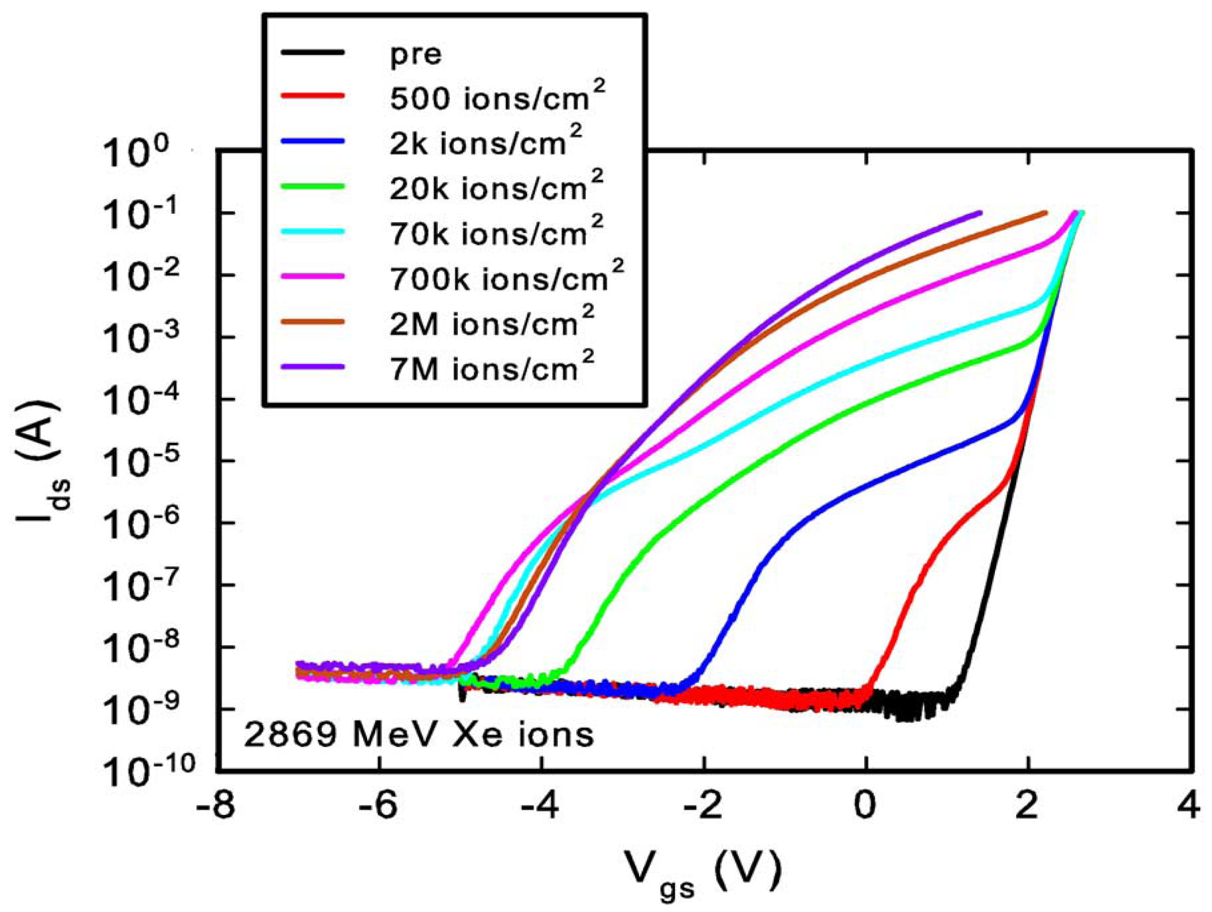
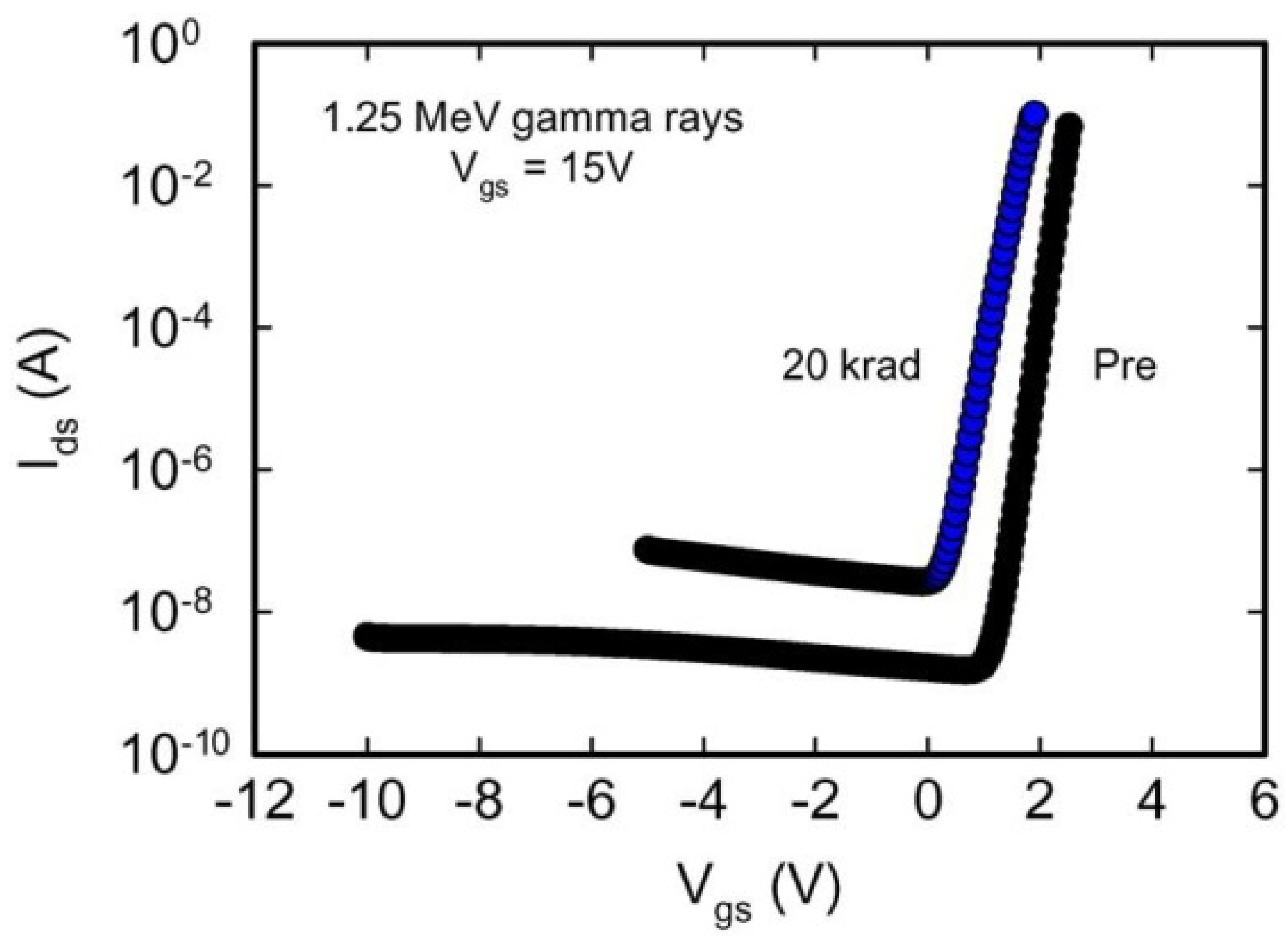
Figure 3 illustrates measured shifts in the subthreshold I–V curves for a typical 30V UMOS power MOSFET due to exposure to Co
60 gamma rays. These particular devices are laid out in a stripe geometry with more than 1000 trenches yielding more than 2000 identical MOS transistors wired in parallel.
Figure 3.
Typical subthreshold I–V curves for a 30V UMOS device pre- and post Co
60 radiation exposure. During exposure, 15V was applied to the gate and all other pins grounded. After ref. [
7].
Figure 3.
Typical subthreshold I–V curves for a 30V UMOS device pre- and post Co
60 radiation exposure. During exposure, 15V was applied to the gate and all other pins grounded. After ref. [
7].
Figure 4 illustrates measured shifts in subthreshold I–V curves for samples of the same 30V UMOS power MOSFET type exposed to a beam of 2869 MeV Xe ions. Felix
et al. [
7] present a detailed description of the experiment and a detailed analysis of the experimental results with the conclusion that the differences between the Co
60 total dose I–V results (
Figure 3) and the heavy ion I–V results (
Figure 4) are due to parasitic transistors that result from microdose deposited by the heavy ions in the UMOS gate oxides. Small parasitic transistors are formed as a single heavy ion passes through the gate oxide generating electron-hole pairs with trapped positive charge resulting at the silicon–oxide interface [
6].
Figure 4.
Typical subthreshold I–V curves for a 30V UMOS device pre Xe heavy ion exposure and after exposure to several fluence levels. During exposure, 5V was applied to the gate and all other pins grounded. After ref. [
7].
Figure 4.
Typical subthreshold I–V curves for a 30V UMOS device pre Xe heavy ion exposure and after exposure to several fluence levels. During exposure, 5V was applied to the gate and all other pins grounded. After ref. [
7].
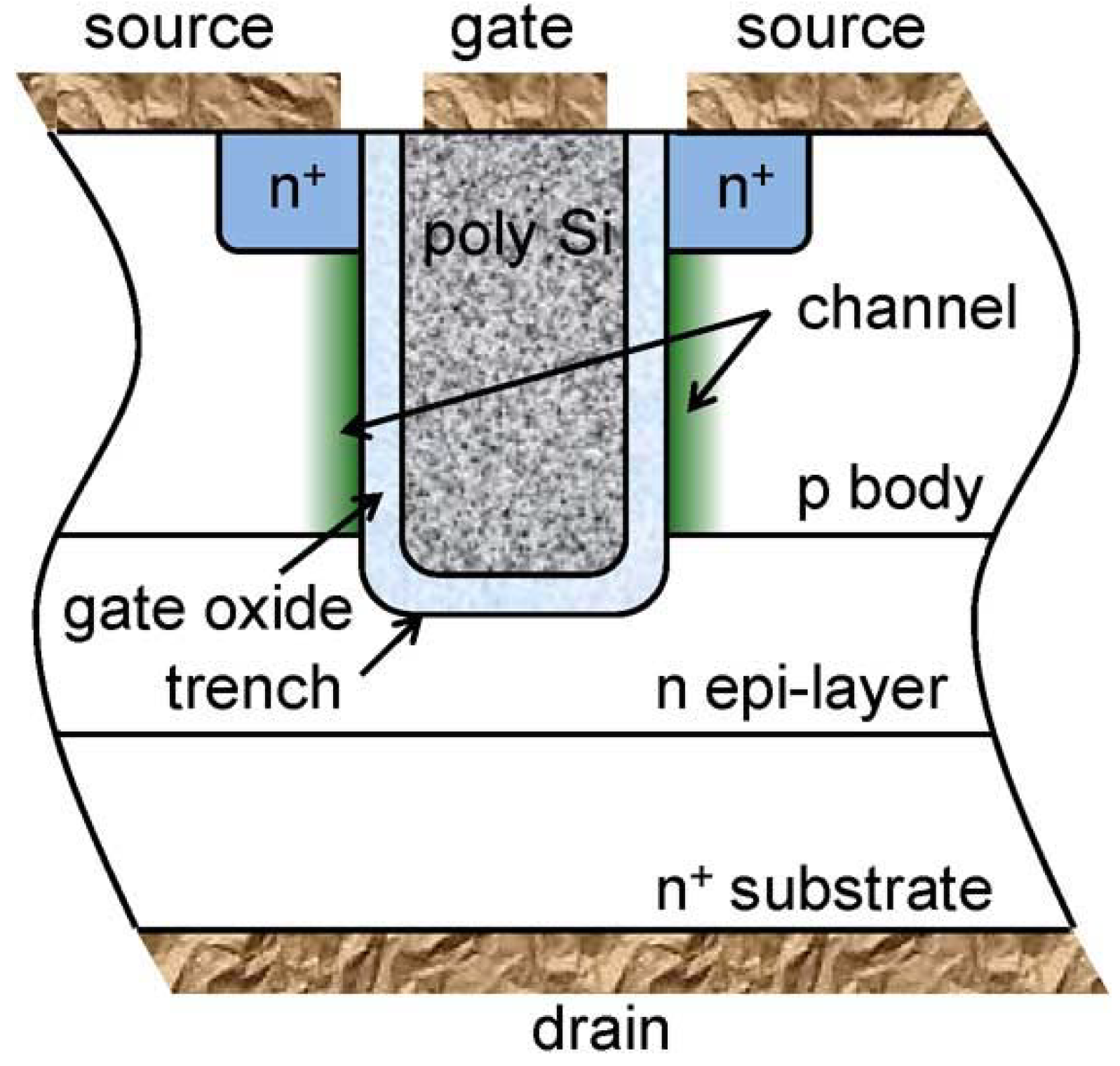
Formation of a parasitic transistor is illustrated in
Figure 5, a cross section for a stripe geometry UMOS power device illustrating a heavy ion passing through the gate oxide along the trench sidewall. Trapped charge in the gate oxide, in the vicinity of the track, would reduce the threshold voltage resulting in unexpected off-state leakage currents.
Figure 5.
Schematic cross section illustrating an ion strike through the gate oxide on the sidewall of the trench in a UMOS power device. After ref. [
7].
Figure 5.
Schematic cross section illustrating an ion strike through the gate oxide on the sidewall of the trench in a UMOS power device. After ref. [
7].
Other investigators have observed similar microdose effects in UMOS power devices [
4,
8,
9] and Griffoni
et al. [
10] have reported microdose effects induced by heavy ion strikes in the sidewall gate-oxide of FinFETs in advanced CMOS devices.
In a 2008 paper, Shaneyfelt
et al. [
11] point out that “… if trench FET power MOSFETS are going to be used in proton-rich space environments, gamma ray testing of the devices could significantly underestimate the radiation-induced degradation, leading to unexpected failures in space environments …”
The tests described here which illustrate the microdose effect were made with the ion beam incident perpendicular to the die surface. This convenient test geometry may not be representative of the direction of an ion (or proton) hit in an actual spaceborne system, thus possibly reducing the probability of this particular degradation mechanism.
4. Single Event Burnout (SEB) Effects in UMOS Technology
SEB in VDMOS and UMOS power devices is an effect dependent on the inherent parasitic BJT in the device structure. SEB is triggered when a heavy ion passes through the power MOSFET biased in the OFF state (blocking a high drain-source voltage). Short-lived transient currents generated by the heavy ion turn on the parasitic BJT [
12,
13]. Due to a regenerative feedback mechanism, collector currents in the BJT increase to the point where second breakdown sets in, creating a permanent short between the source and drain and rendering the MOSFET useless. A key component of the regenerative feedback mechanism is avalanche generated hole current in the collector region of the BJT. A good review of the SEB physics and the techniques used to model SEB in VDMOS power devices has been provided by Johnson
et al. [
14]. SEB in UMOS devices, because of the unique structure, is similar to SEB in BJTs [
15].
SEB in UMOS power devices has been observed experimentally [
9,
16,
17,
18]. Liu
et al. [
17], in extensive tests, noted that the failure signatures of pure SEB failure observed in commercial trench power MOSFETs was very much like the SEB observed on radiation hardened VDMOSFETs. Koga
et al. [
9], in a 2014 paper, note similar results. A recent review paper by Titus [
19] describes test circuits and methodology for such tests. During exposure to heavy ion radiation, the drain leakage current will suddenly increase to the allowed current limit while the gate leakage current remains at the base level. On visual inspection, burnout locations can often be found in the device active area.
Wang
et al. [
20] has used commercial TCAD software to simulate SEB in UMOS devices.
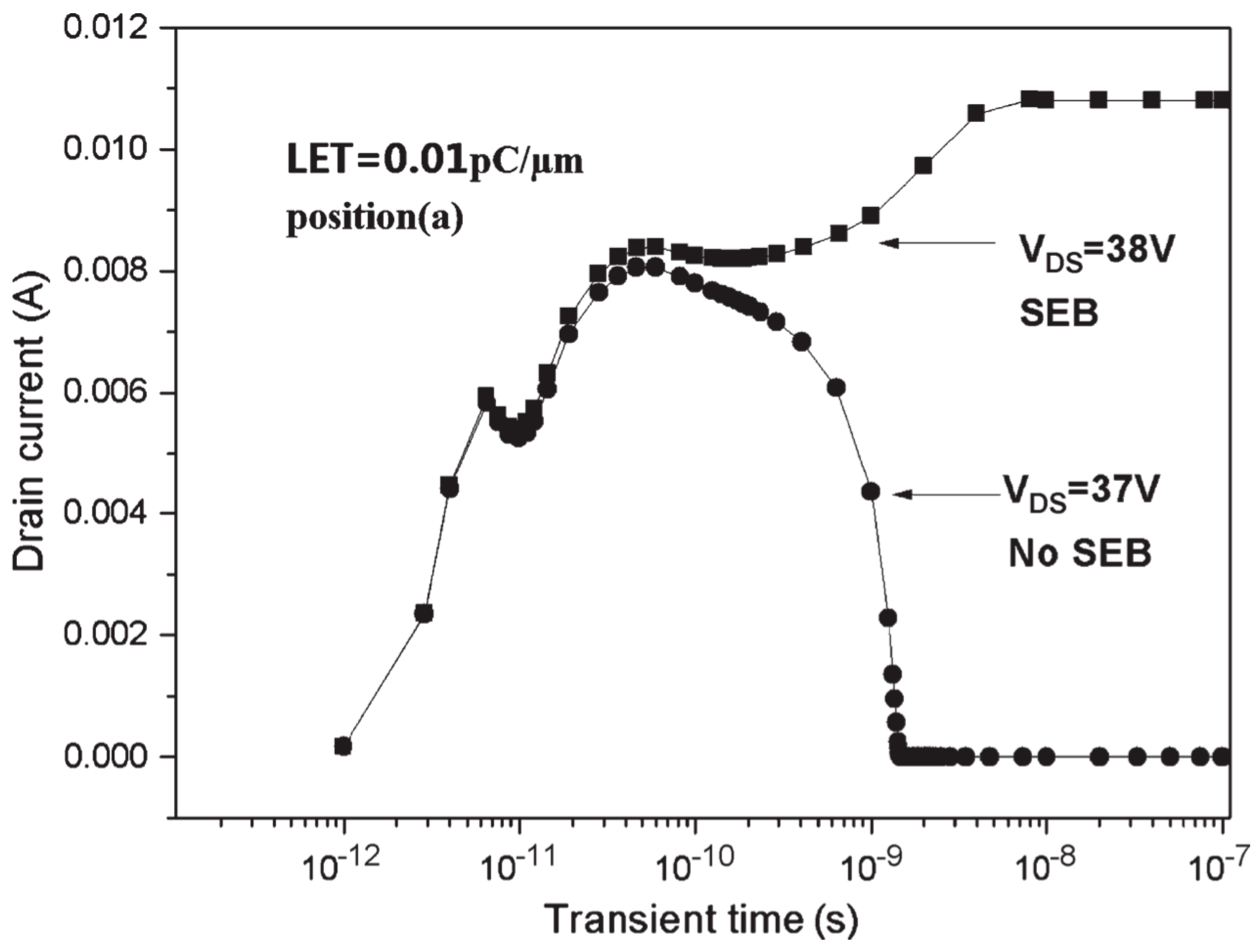
Figure 6 is a cross section of a half-cell of the structure simulated with physical parameters indicated which approximate a UMOS device with breakdown voltage of 70V and threshold voltage of 3V. The authors report that, as expected, drain-source voltage, ion strike position, and LET all figure in determining SEB thresholds and present tables illustrating the effects of varying these parameters on SEB.
Figure 7, from this work, shows the onset of SEB and the sensitivity to drain-source voltage for the ion strike through the gate poly.
For these simulations, the ion strike is assumed to be incident perpendicular to the die. The UMOS SEB simulations [
20] do not explore the results of off perpendicular incident ions. Worst case response may not occur with the incident ion perpendicular to the die surface, but the worst case may be at beam angles almost parallel to the die surface [
21].
Figure 6.
Cross sectional view and doping concentrations used in the Wang
et al. TCAD simulations reported in ref. [
20].
Figure 6.
Cross sectional view and doping concentrations used in the Wang
et al. TCAD simulations reported in ref. [
20].
Figure 7.
Drain current versus time for a 70V UMOSFET illustrating the on-set of SEB and the sensitivity to drain-source voltage. Ion strike is assumed to be incident perpendicular to the die and near the center of the trench. After ref. [
20].
Figure 7.
Drain current versus time for a 70V UMOSFET illustrating the on-set of SEB and the sensitivity to drain-source voltage. Ion strike is assumed to be incident perpendicular to the die and near the center of the trench. After ref. [
20].
Wang
et al. in other work [
22] have used TCAD simulation to explore SEB hardening strategies for UMOSFETs. Simulations indicated that enlarging the p
+ plug and the addition of a buffer layer between the epitaxial layer and substrate can reduce SEB susceptibility with the buffer layer making the most difference. These results are similar to results obtained for VDMOS devices [
19]. Using TCAD simulation, Wang
et al. [
23] have also been able to explore the potential for hardening using alternate structural configurations such as including a Schottky source plus an N-type buffer layer. They report that the threshold voltages for burnout are markedly increased making the devices less sensitive to SEB when compared to the burnout voltage of the base UMOS structures simulated [
20].
5. Single Event Gate Rupture (SEGR) in UMOS Technology
SEGR is due to localized dielectric breakdown of the gate oxide [
24,
25,
26]. Under appropriate bias conditions, accumulation of charge (generated by the heavy ion) in the silicon at the silicon-silicon oxide (Si-SiO
2) interface can result in a sufficiently high electric field across the gate oxide to cause gate rupture. SEGR is a destructive effect. As soon as the minimum voltage (SEGR threshold) required for SEGR to occur has been reached and passed, SEGR occurs almost instantly [
26]. The peak electric field occurs in picoseconds of the ion passage through the structure. A good review of the SEGR physics and the techniques used to model SEGR in VDMOS power devices has been provided by Johnson
et al. [
14].
SEGR in UMOS power devices was experimentally observed by Koga
et al. [
9] and Liu
et al. [
16,
17] in addition to measurements of SEB. Wang
et al. [
20] simulated SEGR in UMOS devices using the framework developed by Allenspach
et al. [
24,
25].
Figure 6 is a cross section of a half-cell of the structure simulated.
In the Allenspach method, the critical electric field across the gate oxide required for onset of SEGR is related to the gate oxide thickness and the LET of the incident ion using a modified version of an empirical model first elucidated by Wrobel [
27]. Then, 2-D simulations are used to determine (1) the peak electric field following the ion strike and (2) the pre-strike field in the gate-oxide for a specified set of bias conditions and oxide thickness. The maximum transient component of the oxide electric field can then be computed and compared to the critical electric field required for the onset of SEGR. This information allows mapping of bias conditions that allow safe operation or, conversely, device bias conditions that result in SEGR.
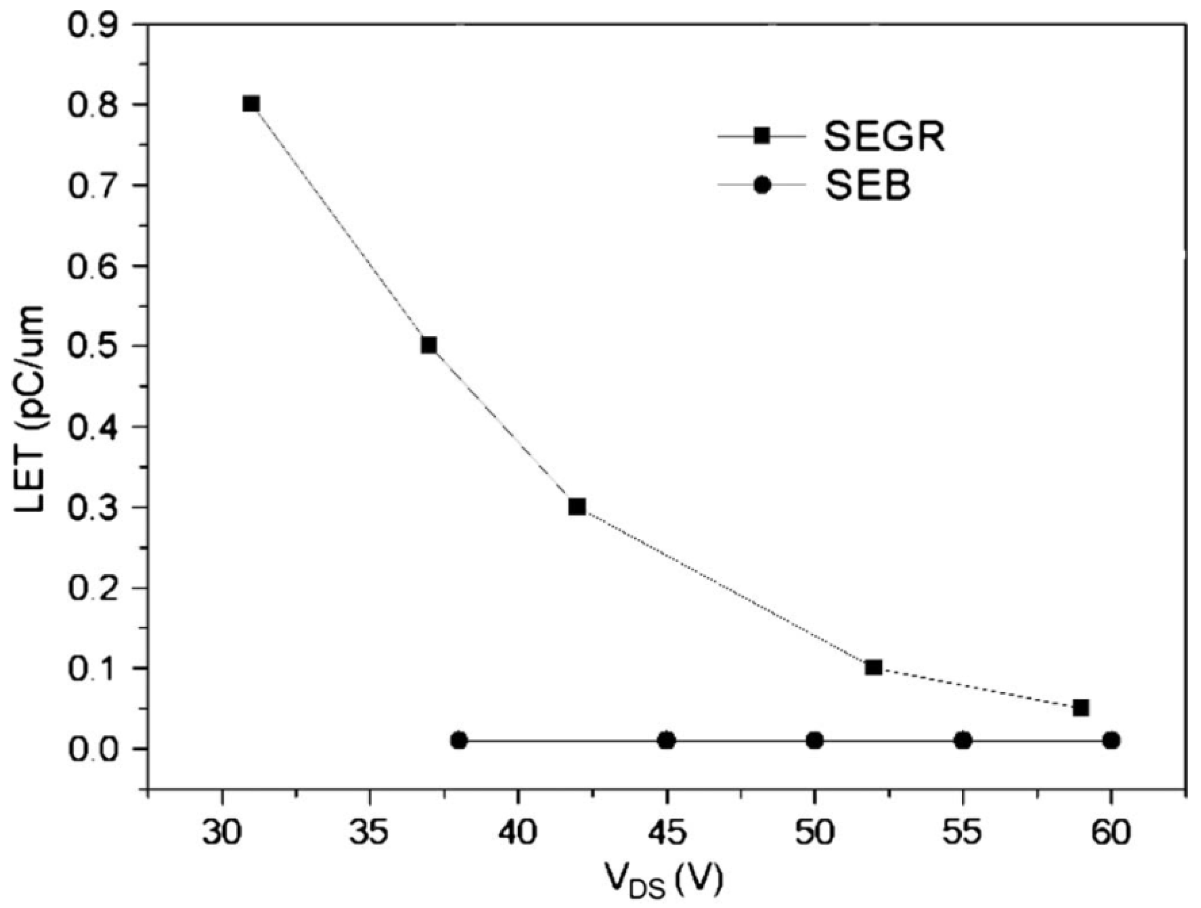
Figure 8 from [
20] displays drain-source voltage that is the threshold for triggering SEGR or SEB in the 70V UMOSFET simulated as a function of incident ion LET. The ion strike is assumed to be incident perpendicular to the die and through the gate material near the center of the trench. Not surprisingly, the threshold for SEGR increases as LET decreases.
In a VDMOS device, the physical location of the actual gate rupture is assumed to be near where the ion strike passes through the gate oxide [
28]. However, in the SEGR simulations of Wang
et al. [
20], the heavy ion is incident perpendicular to the die surface and passes through the gate poly and the bottom of the trench and the authors say that “a portion of the holes will be accumulated along the sidewalls of the trench near the bottom.” This leaves some uncertainty as to the physical location of the gate rupture. Does the simulation indicate that the oxide breakdown occurs at the bottom of the trench or on the sidewall of the trench?
As in SEB failures, worst case response for SEGR may not occur with the incident ion perpendicular to the die surface, but the worst case may be at beam angles near parallel to the die surface [
21]. Liu
et al. [
17] observed a higher probability of SEGR failure at beam angles tilted from the perpendicular. It would be interesting to see TCAD simulations of this failure extended to cases where the incident ion was not perpendicular to the UMOS device die.
Figure 8.
Threshold drain-source voltage for triggering SEGR or SEB in a 70V UMOSFET as a function of incident ion LET. Ion strike is assumed to be incident perpendicular to the die and near the center of the trench. After ref. [
20].
Figure 8.
Threshold drain-source voltage for triggering SEGR or SEB in a 70V UMOSFET as a function of incident ion LET. Ion strike is assumed to be incident perpendicular to the die and near the center of the trench. After ref. [
20].
6. Discussion
UMOS power device technology has been shown by experiment to have vulnerabilities to SEB, SEGR, and microdose. Concern for the heavy-ion vulnerability of UMOS power devices in comparison to similarly rated VDMOS devices has been expressed [
7,
11,
16]. Liu
et al. [
16] examined several devices in the 30–200 V range. The Lauenstein
et al. [
18] results were for a 250 V device. Neither group has published detailed experimental results in the open literature. Koga
et al. [
9] present results for two different 100V devices with cross-section data and I–V data. No research team has published detailed radiation-effects comparisons of UMOS devices with similarly rated VDMOS devices. The simulations by Wang
et al. [
20] are for a hypothetical 70V device; there are no comparisons with experimental results.
Since there are significant differences in device structure and device physics between the VDMOS and UMOS technologies, understanding of the physical mechanisms of heavy-ion radiation degradation and failure of silicon UMOS power transistors would benefit from the publication of more detailed experimental studies of SEB and SEGR in UMOSFETs. This data coupled with TCAD modeling informed by experimental results should provide insights for improving UMOS device designs for survivability and provide validated protocols for utilization of these devices in spaceborne systems. Nevertheless, some radiation tolerant UMOS power products have been introduced in the commercial marketplace.
Additionally, with evidence that device bias voltages at which SEB and SEGR occurs in VDMOS (or the determination of a device’s safe operating area) may be linked to the ion energy and ion species [
19,
29,
30] rather than linked solely to the LET of the ion, worst-case conditions for radiation hardness assurance testing and qualification of UMOS power transistors for use in space should be carefully examined.
7. Conclusion
This review has summarizes the current state of knowledge regarding the degradation and/or failure of silicon trench (or UMOS) power transistors due to heavy-ion exposure (or energetic proton environments) such as encountered in spacecraft. Published work has demonstrated UMOS power device technology vulnerabilities to SEB, SEGR, and microdose. The physics of microdose degradation is well understood. The physics of SEB and SEGR failure of UMOS devices appears to be similar to that of VDMOS devices; however, some interesting questions remain. Additional experimental results and refinement of the models for simulation would allow improvement of UMOS device designs for survivability and provide guidelines for selection of these devices for spaceborne systems.
