Article

Current-Perpendicular-to-Plane Magnetoresistance in Chemical Vapor Deposition-Grown Multilayer Graphene

Department of Electrical and Computer Engineering, University of Alberta, Edmonton, AB T6G 2V4, Canada
*
Author to whom correspondence should be addressed.
Electronics 2013, 2(3), 315-331; https://doi.org/10.3390/electronics2030315
Submission received: 13 June 2013 / Revised: 13 August 2013 / Accepted: 16 August 2013 / Published: 11 September 2013
(This article belongs to the Special Issue Carbon Nanoelectronics)

Abstract

:
Current-perpendicular-to-plane (CPP) magnetoresistance (MR) effects are often exploited in various state-of-the-art magnetic field sensing and data storage technologies. Most of the CPP-MR devices are artificial layered structures of ferromagnets and non-magnets, and in these devices, MR manifests, due to spin-dependent carrier transmission through the constituent layers. In this work, we explore another class of artificial layered structure in which multilayer graphene (MLG) is grown on a metallic substrate by chemical vapor deposition (CVD). We show that depending on the nature of the graphene-metal interaction, these devices can also exhibit large CPP-MR. Magnetoresistance ratios (>100%) are at least two orders of magnitude higher than “transferred” graphene and graphitic samples reported in the literature, for a comparable temperature and magnetic field range. This effect is unrelated to spin injection and transport and is not adequately described by any of the MR mechanisms known to date. The simple fabrication process, large magnitude of the MR and its persistence at room temperature make this system an attractive candidate for magnetic field sensing and data storage applications and, also, underscore the need for further fundamental investigations on graphene-metal interactions.

1. Introduction

Magnetoresistance (MR), the change in electrical resistance of a solid-state system as a function of an external magnetic field, is a key effect in condensed matter physics, both for fundamental understanding of charge transport phenomena, as well as immense commercial implications [1,2]. Transition metals and their alloys often show anisotropic MR that originates from spin-dependent scattering, due to spin-orbit interactions [3]. Metals and semiconductors exhibit ordinary classical MR [1] and, also, more exotic MR originating from quantum effects, such as weak localization and anti-localization [4]. Spin-dependent scattering in ferromagnet/non-magnet multilayered structures is the key physics behind the operation of giant magnetoresistive (GMR) devices and spin valves, which are ubiquitous in state-of-the-art read heads and magnetic random access memories [2]. Other notable MR effects include, but are not limited to, inhomogeneity-induced MR (semiconductors) [5], organic MR (polymers and small-molecular organics) [6], colossal MR (perovskite compounds) [7] and hopping MR (disordered solids) [8].
MR in graphitic systems (single to a few layers of graphene and bulk graphite) has drawn significant attention in recent years. Both current-in-plane (CIP) and current-perpendicular-to-plane (CPP) geometries have been studied with various orientations of the external magnetic field [9,10,11,12,13,14,15,16,17,18,19,20,21]. For highly-oriented pyrolytic graphite (HOPG), a positive MR is generally observed at low fields, with the magnetic field normal to the graphitic plane (parallel to the c-axis) [11]. MR in graphitic samples has been shown to deviate from Kohler’s law [11]. Magnetic field-driven metal-insulator transition has been observed in the in-plane and out-of-plane resistivities of graphite, with the field parallel to the c-axis [11,12]. An explanation of the metal-insulator transition has been offered in [13,14]. This explanation is based on magnetic field-induced breaking of the chiral symmetry and gap-opening in the spectrum of the Coulomb interacting quasiparticles at the corners of the Brillouin zone. This effect is interpreted as the enhancement of the fermion dynamical mass through electron-hole pairing, i.e., a transition to an excitonic insulating state [15]. Such metal-insulator transitions are absent when the magnetic field is parallel to the plane [15]. Multilayer graphene (MLG) samples, on the other hand, generally exhibit a negative MR at low magnetic fields, due to the weak localization effect [16,17,18,19,20]. As consistent with this picture, a negative MR has been found to decrease with increasing temperature, due to the reduction of phase coherence time [16,17,18,19,20]. In some cases, a positive MR has been reported in MLG samples at higher fields, which can have diverse physical origins, such as an excitonic gap in the Landau level [16], weak anti-localization [17,18] and classical and quantum linear MR [20,21].
Very recently, graphene has been integrated with ferromagnetic electrodes to realize novel hybrid magnetoresistance devices that work on the principle of spin-polarized carrier injection, transport and detection. For example, [22] reported graphene-based magnetic tunnel junctions in which single-layer graphene is sandwiched between two ferromagnetic electrodes (NiFe and Co). The graphene layer was synthesized using a CVD process on a Cu substrate and was physically transferred between the ferromagnetic contacts to produce the magnetic tunnel junction. Tunneling MR of ~0.4% has been reported in these devices at room temperature. In [23], graphene tunnel barriers have been used to inject spin-polarized carriers within silicon from ferromagnetic contacts. Thus, the graphene monolayer can be used to circumvent the “conductivity mismatch” problem that prohibits efficient spin injection from metal ferromagnets to semiconductors [24]. Apart from these applications, a graphene-coated nickel surface has been shown to perform as an oxidation-resistant spin polarizer, which can be integrated with spin valves or magnetic tunnel junctions to achieve superior MR ratios [25]. An extraordinary MR (EMR) has also been reported in metal-shunted CVD-grown graphene devices [26]. An EMR of ~600% has been observed at ~12 T and liquid Helium temperature.
In most of the studies cited above, graphene samples have been prepared by either mechanical exfoliation [16,18,19] or chemical vapor deposition (CVD) [20,21,22,23,25]. In the latter case, graphene is generally grown on a catalytic surface (commonly Ni [25] or Cu [20,22]). Next, the catalytic surface is removed by an appropriate chemical etchant, and graphene is transferred on some suitable electrode. However, several studies have indicated that the graphene-metal catalyst interface has rich underlying physics and can give rise to novel effects, such as “perfect spin filtering” [27,28] and “giant Rashba splitting” [29]. Exploration of the effects that rely on the graphene-metal catalyst interaction clearly requires the presence of the catalyst, and the above-mentioned etching step must be avoided.
Depending on the nature of the interaction, graphene-metal interfaces can be broadly classified into two categories: the physisorption interface and the chemisorption interface [30,31,32,33]. Metals, such as Al, Cu, Ag, Au and Pt, typically form a “physisorption interface” with graphene [30,31,32,33]. Such an interface is characterized by weak bonding and charge transfer between the metal and graphene, which results in doping and a shift in the Fermi level from the Dirac point. For physisorption interfaces, the electronic structure of graphene remains essentially unperturbed, and hence, such contacts are ideal for probing the (magneto-) transport properties of pristine graphene [32,34,35]. “Chemisorption interface”, on the other hand, is characterized by a strong chemical bond between graphene and metal (Co, Ni), with a concomitant modification of the electronic structure of pristine graphene, including elimination of the Dirac point, band gap opening and creation of metal-graphene hybrid localized states in the gap [30,31,32,33]. For graphene epitaxially grown on (111) Ni [36,37,38,39,40], chemisorption occurs, due to hybridization of Ni 3d and C 2pz orbitals, which are elongated normal to the plane and have a significant overlap, due to small interfacial distance (~2.07 Å [31]) between the Ni surface and graphene. In spite of the detrimental effect on the graphene electronic structure, chemisorption interfaces are crucial elements for graphene-based spintronics. For example, energy-level alignment at the (111) Ni-graphene interface promotes transmission of only minority spins, resulting in perfect spin filtering [27,28]. Further, chemisorption interfaces enhance spin-orbit effects at the interface, and magnetization can be induced to the carbon atoms [41]. Such effects can have a pronounced impact on the MR of graphene-metal chemisorption interfaces. To our knowledge, however, very few (if any) studies exist that address the MR properties of graphene-metal composite systems.
In this work, we report CPP-MR effects in multilayer graphene (MLG), CVD-grown on Ni and Cu substrates. As mentioned before, a chemisorption interface is formed in the former case, whereas a physisorption interface is formed in the latter case. In the CPP geometry, the charge carriers directly interact with the graphene-metal interface. We find a novel giant negative CPP-MR for MLG grown on Ni. Similar effects are absent for MLGs that are grown on Cu. Combined with the control experiments, graphene-substrate chemical interaction appears to play a key role behind the observed giant, negative MR effect.
This article is organized as follows. In the next section, we describe the experimental details, followed by presentation of the results and the discussion in Section 3. We conclude in Section 4 by highlighting the key findings of this investigation.

2. Experimental Section

Device fabrication consists of the following steps. A schematic description of these steps is shown in Figure 1a.
Figure 1. (a) Schematic description of the fabrication process and (b) the device schematic showing multilayer graphene (MLG)/metal catalyst heterojunction and the measurement configuration. The inset of Figure 1(a) shows the typical XRD (X-ray diffraction) spectrum of the Ni substrate. The metal catalyst in Figure 1(b) is either Ni or Cu. The MLG is grown on the bottom metal catalyst (Ni/Cu) by chemical vapor deposition (CVD). Current-perpendicular-to-plane (CPP) resistance (Rzz) is measured between the top Ag contact and the bottom metal catalyst substrate. In our experiment, the external magnetic field (B) is either parallel to the current (I), i.e., θ = 0, or perpendicular to the current, i.e., θ = π/2.
Electronics 02 00315 g001

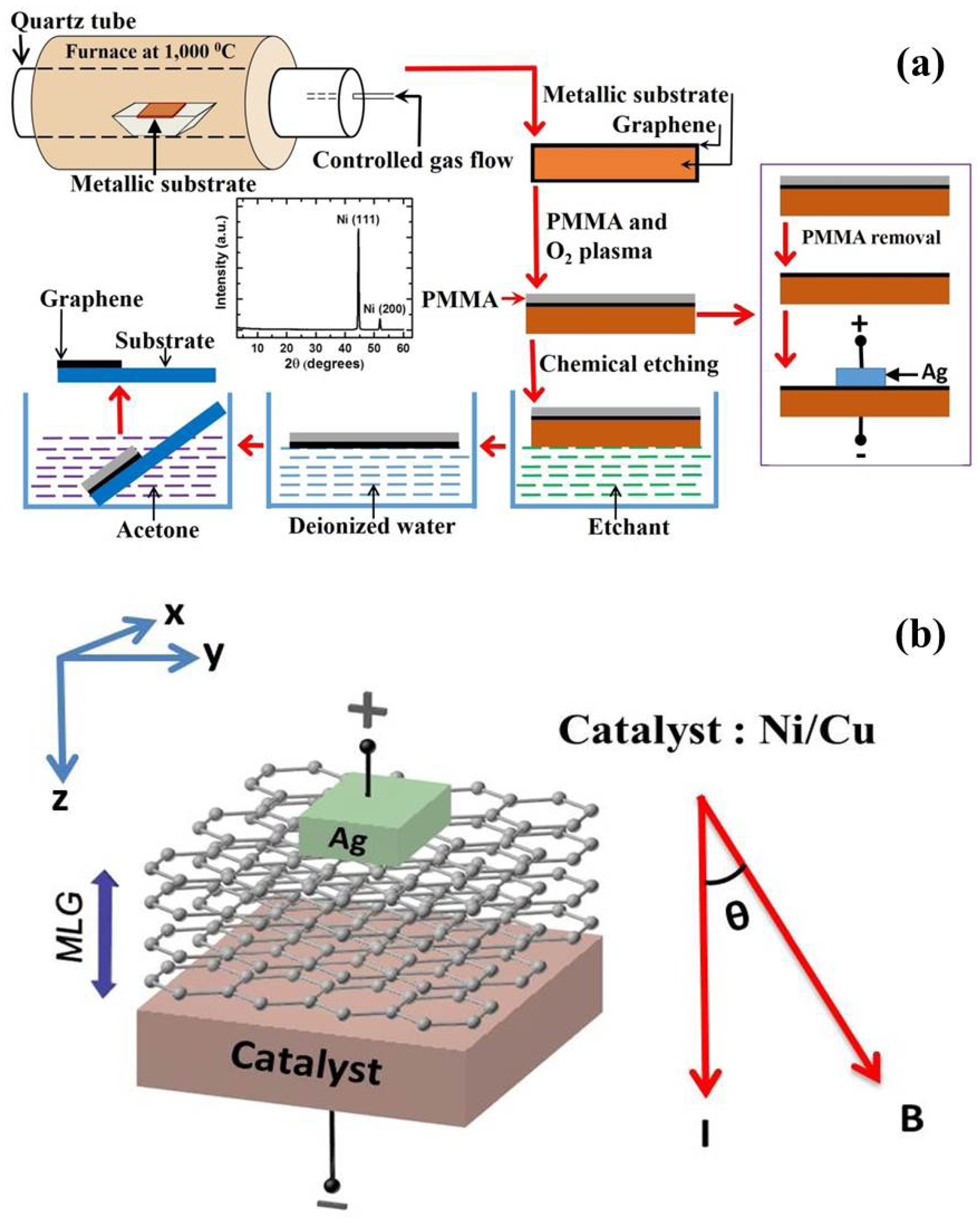
2.1. Growth of Multilayer Graphene (MLG) on Ni and Cu Substrates Using CVD

Multilayer graphene (MLG) has been grown on polycrystalline (predominantly (111), as shown in the XRD data in Figure 1a) Ni substrates (25 µm thick, annealed, 99.5% metal basis, purchased from Alfa Aesar) in a commercial Tystar chamber using a standard CVD method. Various groups have used similar polycrystalline Ni substrates in the past for graphene growth [36,37,38,42]. The in-plane lattice constant in the (111) Ni plane (0.232 nm) matches closely with that of graphite (0.246 nm), allowing continuous growth of graphene layers over the entire Ni surface during the CVD process. The CVD process flow consists of the following steps: (a) Ni foil (~2 cm × 2cm) in size load; (b) furnace purge, (c) temperature ramp to 1000 °C and hydrogen anneal for one hour; (d) graphene growth at 1000 °C for 10 min; (e) natural cooling; and, finally, (f) unloading of the sample. We have used 0.3% CH4, 9.7% H2 and 90% Ar during the growth of graphene. A higher concentration of carbon-containing species within the chamber leads to bulk graphite growth on the Ni surface [42].
MLG on copper foil has been acquired from ACS (Advanced Chemical Supplier) materials. The growth process of graphene on copper foil has been discussed in detail in the literature [43].

2.2. Oxygen Plasma Etching of MLG and Device Patterning

During the CVD process, MLG growth takes place on both sides of the substrate catalyst. To prepare the MLG-covered catalytic substrate for CPP measurement, we need to remove MLG from one of the planar surfaces. For this purpose, a protective polymethyl methacrylate (PMMA) layer is coated on the top surface of the MLG, and the sample is subjected to oxygen plasma etching (Figure 1a). This process removes MLG from all other surfaces, and the MLG under the PMMA layer is preserved. Next, the PMMA layer is removed using acetone, and electrical contacts are made on top of the MLG surface and the bottom of the catalytic substrate (Figure 1a,b).
We have also prepared and tested several control samples in which the CVD-grown MLGs have been transferred on a separate substrate (described below). This is achieved by chemically etching the metal catalyst. Before this chemical etching step, the above-mentioned oxygen plasma etching needs to be performed, so that the etchant can come in contact with the metal catalyst and initiate the etching process.

2.3. Transfer of MLG on SiO2/Si

The transfer of MLG has been performed as follows (see Figure 1a). The Ni (Cu) substrate is etched away using ferric chloride (ammonium persulfate) etchant. In the case of Ni, the etchant needs to be heated up slightly (~60 °C) to expedite the etching process. Upon completion of the etching step, graphene/PMMA composite film floats up in the etchant solution. Graphene/PMMA film is collected and thoroughly cleaned in deionized water. Next, the cleaned graphene/PMMA film is transferred on a SiO2 (300 nm)/Si wafer. After overnight drying, the sample is heated on a hot plate, so that the graphene layer adheres strongly to the SiO2 surface and allows reliable electrical measurements. Finally, the top PMMA layer is dissolved in acetone, which leaves only the graphene layer on the SiO2 surface. We estimated the number of graphene layers to be ~300 from step height measurements.
Figure 2 shows the Raman spectra from representative regions of the MLG before and after transferring on SiO2/Si. Similar techniques have been used to transfer graphene on patterned electrodes. In such transferred samples, no formation of a “chemisorption interface” between graphene and the substrate is expected, and these devices, therefore, serve as control samples.
Figure 2. Raman spectroscopy of epitaxially-grown MLG. (a) CVD-grown MLG on polycrystalline nickel; and (b) CVD-grown MLG on copper. Data from before and after transferring the MLG on SiO2/Si are presented. The excitation wavelength is 532 nm. In (a), the 2D peak is symmetric before the transfer and can be fitted with a single Lorentzian (top inset). The 2D peak becomes asymmetric (bottom inset, Figure 2(a)) after the transfer, which is due to the high temperature etching process. In (b), the 2D peak is symmetric, even after the transfer, and can be fitted with a single Lorentzian (inset). A background signal from the Cu substrate is present before the transfer.
Electronics 02 00315 g002

3. Results and Discussion

Figure 1b shows the device schematic and the measurement geometry. The substrate (Ni or Cu) is used as a catalyst for graphene growth in the CVD process. In order to incorporate the effect of the graphene-metal interface in the CPP-MR measurements, we used the catalytic substrate itself as the bottom electrode. As discussed above, significant interfacial chemical bonding is expected in the case of MLG on Ni samples, but no such effect is expected for MLG on Cu. Another contact is fabricated at the center of the top MLG surface using silver epoxy with a contact area of ~1 × 1 mm2. CPP resistance (Rzz) is measured between these two contacts by a conventional two-wire DC method at a constant current bias of 1 mA. The contact resistance of the device is ~1% of the total device resistance, and the contacts showed no significant magnetoresistance, except the anisotropic magnetoresistance (AMR, ~1%) of Ni (data not shown). As shown in Figure 1b, the device current (I) is always perpendicular to the MLG plane. In this study, we have considered two orientations of the magnetic field, (B): (i) B || I (i.e., θ = 0) and (ii) B Electronics 02 00315 i001 I (i.e., θ = π/2).
Figure 2 presents the typical Raman spectroscopic characterization of CVD-grown MLGs, before and after transfer on SiO2/Si. The Raman features presented here are representative of the entire MLG surface. The absence of the D peak (1360 cm−1) indicates very low defect density in these samples. The most distinct peaks are the G peak (~1580 cm−1) and the 2D peak (~2700 cm−1). The prominent G peak indicates the presence of a graphitic hexagonal lattice structure over the entire surface. In Figure 2a, the position of the 2D peak is upshifted, and its full width at half-maximum (FWHM) is wider (~50 cm−1) than that of single-layer graphene (~35 cm−1) [38]. The relative intensity of the 2D peak to that of the G peak is <1 over the entire surface. These features indicate the formation of multilayer graphene (MLG) [38,44,45], which has been independently confirmed by removing the metal catalyst and transferring the graphene onto the SiO2/Si substrate.
However, despite the presence of multiple graphene layers, the 2D line shape is symmetric and can be fitted by a single Lorentzian for both MLG on Ni and MLG on Cu specimens. We have never observed the multi-peaked and “shouldered” 2D band in these samples, which is the hallmark of HOPG and HOPG-derived multilayer graphene [44,45]. For HOPG and HOPG-derived MLGs, the electronic dispersion is split, due to strong interlayer coupling, which results in a multi-peaked and “shouldered” 2D band [44,46,47]. Absence of such features in the 2D band of Figure 2 is direct experimental evidence that in our samples, interlayer coupling is significantly weaker compared to HOPG [44,46]. The CVD-grown samples, therefore, resemble “turbostratic” graphite [44,48,49]. We note that weak interlayer coupling and the resulting symmetry of the 2D peak is a common feature of CVD-grown MLGs and has been reported by many groups in the past [38,44,48,49].
The symmetric 2D peak of MLG-on-Cu samples remains unchanged, even after transferring the MLG on SiO2/Si, but slight asymmetry has been observed for the MLG transferred from Ni (Figure 2). This difference originates from the differences in the transfer process used for these two samples. In the case of MLG on Ni, the Ni substrate has been etched away by prolonged etching in hot FeCl3 solution. Such high temperature etching was not necessary for MLG on Cu samples. It is well known that heat treatment makes the 2D peak asymmetric, due to thermal stress [50]. Our data is consistent with this observation.
Figure 3a–d present the angle-dependent MR response of MLG on Ni devices in the temperature range 10–200 K. We have tested several devices and observed that the MR response is strongly dependent on the direction of the external magnetic field. In Electronics 02 00315 i002 
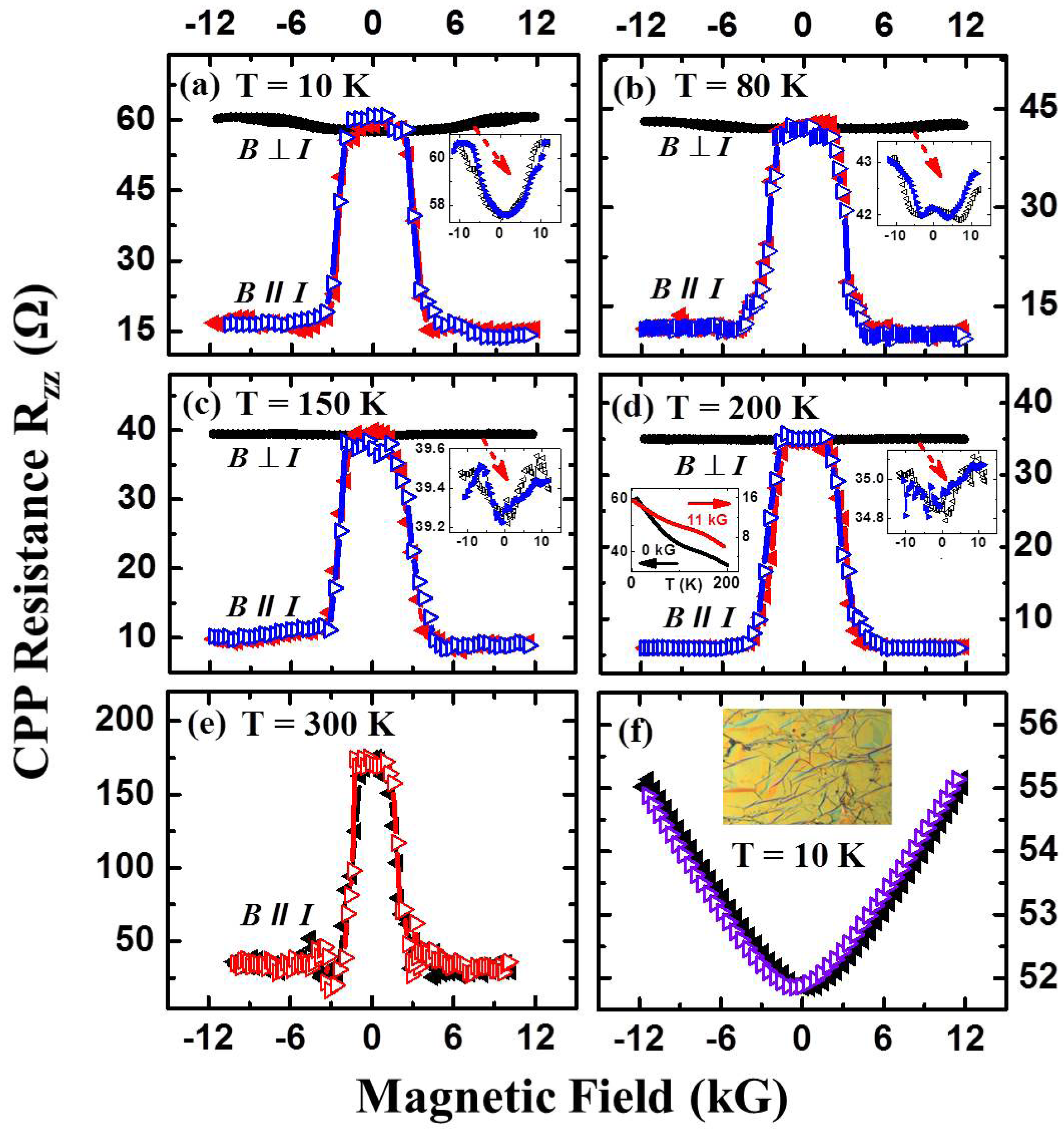
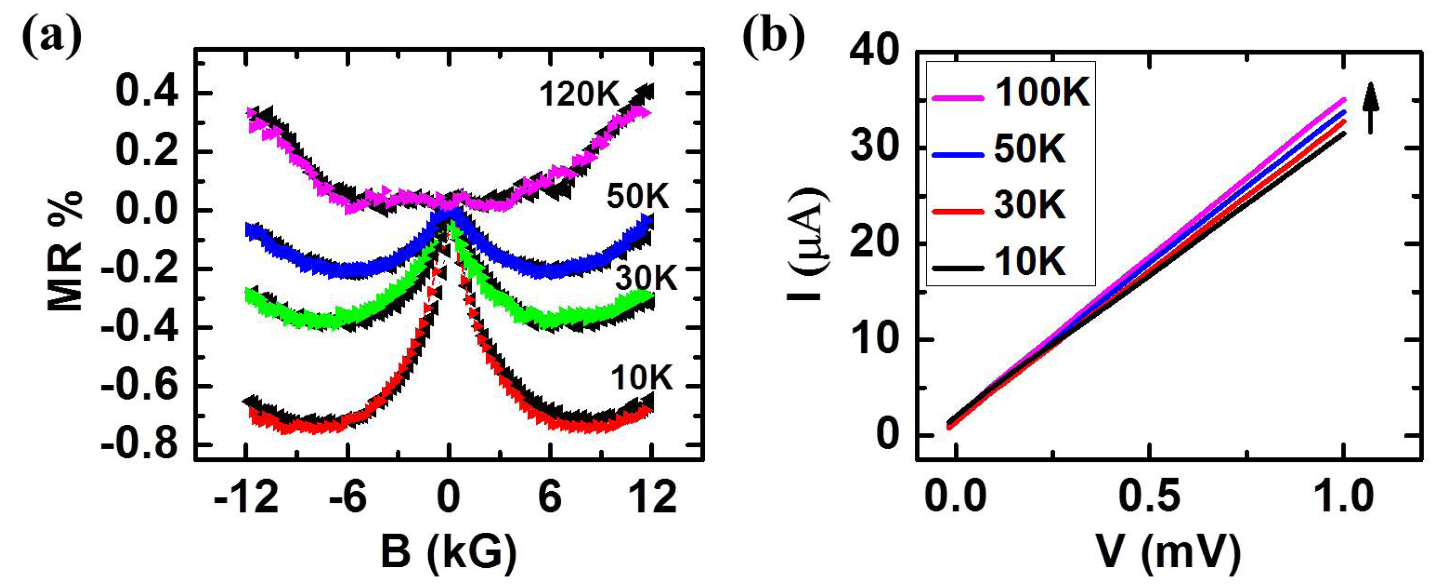
geometry (i.e., “field-in-plane” or θ = π/2), a weak, positive MR is observed (insets of Figure 3a–d), which gradually disappears as the temperature increases. This positive MR has been observed before and is the result of the bending of carrier trajectories, due to classical Lorentz force [20]. Surprisingly, in B || I geometry (i.e., “field normal to the plane” or θ = 0), a sharp decrease in resistance (a factor of three) at around 3 kG is observed as the magnetic field is increased. Such a large change in resistance cannot be explained by semiclassical models, since the Lorentz force on charge carriers is zero in B || I geometry. Both scan directions up to ±1 Tesla are presented to demonstrate the reproducibility of the data and the absence of any hysteresis. We note from the MR data of several nominally identical samples that the observed effect is almost independent of temperature, which sometimes even persists at room temperature. The room temperature MR data from another sample is shown in Figure 3e. The change in resistance is large, around 3 kG, which has been observed in several nominally identical samples (~20) at a similar temperature range. A maximum of a two orders of magnitude change in negative MR has been observed in some of the samples. No hysteretic MR has been observed in any of the samples.
Figure 3. CPP resistance (Rzz) of MLG on Ni devices in the temperature range 10–200 K. (ad) Large negative MR, which is almost independent of temperature, is observed in B || I geometry. For each temperature, MR for both field orientations (B || I and B Electronics 02 00315 i001 I) is shown. The left inset in (d) shows the temperature dependence of CPP resistance at zero and high magnetic fields; (e) room temperature large, negative MR data observed in another MLG on Ni sample; (f) Rzz vs. B for Ni-grown MLG after transferring on the Cu substrate. No negative MR is observed. (Inset) Optical microscopic image of MLG transferred on the Cu substrate. A constant current bias of 1 mA is applied for all resistance measurements. Each resistance value is an average of 50 readings. Both scan directions are presented, and no MR hysteresis is observed.
Electronics 02 00315 g003
The large, negative MR described above cannot be explained by invoking the weak localization effect, which usually gives rise to weak, negative MR (CPP geometry) in graphene [20]. The weak localization effect decreases with increasing temperature, due to a decrease in phase coherence time [20]. On the contrary, the large, negative MR observed in our samples is almost independent of temperature and even persists at room temperature. Further, the angle dependence of the MR in our case is qualitatively different from that expected in the case of weak localization [20].
Another mechanism that can give rise to large, negative CPP MR is interlayer tunneling between the zero mode Landau levels of the constituent graphene layers [51,52,53,54]. This mechanism requires interlayer coupling between the graphene layers to be weak, so that each layer can be viewed as a two-dimensional massless Dirac electron system. In the presence of an external magnetic field, CPP charge transport occurs between the zero mode Landau levels of each layer. The external magnetic field increases the degeneracy of the Landau levels, which results in a large tunneling current and, hence, suppression of device resistance and a negative MR. As discussed before, the Raman data of MLG on Ni samples indeed exhibit a symmetric 2D peak, which suggests weak interlayer coupling in this system. However, this model does not directly take into account graphene-substrate interactions and predicts that CPP resistance (Rzz) is inversely proportional to the magnetic field [51,52,53]. In the present case, we observe a much more sharp decay in resistance at ~3 kG, which does not agree with this prediction. Clearly, further theoretical and experimental research is needed to fully understand the observed negative MR effect.
The so-called “Bright model” [55] discussed negative MR in disordered carbon, which is characterized by a two-dimensional band structure and density of states. Negative MR originates because of magnetic field-induced changes in the density of states, which lead to increased carrier concentration with the field and a concomitant suppression of device resistance. We note that an essentially similar physical picture has been presented in [51] and subsequent work by other groups [52,53]. Another common feature between [55] and [51] is the assumption of the collision-broadened Landau levels. However, there are two features in [55] that are not present in [51]: (1) the presence of shallow acceptor levels, due to defects, and (2) the presence of extra density-of-states at the zero mode Landau level, due to partial three-dimensional ordering of the constituent graphene layers. We note that Bright’s model predicts significantly smaller negative MR, approximately 2% at low temperatures. This effect slowly varies as a function of the magnetic field. In our case, we observe a sharp change in device resistance at a magnetic field of ~3 kG. Further, the MR effects observed in our specimens are significantly stronger (>100%) than that predicted by Bright’s model. Thus, Bright’s model cannot be applied directly to explain our experimental data. We note that Bright’s model does not include the effect of hybridization between the substrate and the interfacial graphene layer. Based on our experimental data (discussed below), we believe that this is a critical component behind the observed effect and must be included in the theoretical model.
We observe from Figure 3d (inset) that the temperature (T)-dependence of CPP resistance, Rzz, shows an insulating behavior (dRzz/dT < 0) for both the zero field and high field (~1 Tesla). This data clearly rules out magnetic field-induced metal-insulator transition as the possible cause behind the observed MR. Previous studies on highly-oriented pyrolytic graphite (HOPG) or HOPG-derived MLG samples modeled CPP charge transport as a combination of in-plane transport in the constituent layers and phonon- or impurity-assisted interlayer charge transfer [56,57]. If the in-plane transport is dominant (which typically occurs at higher temperatures), then dRzz/dT > 0, whereas dRzz/dT < 0 if the in-plane movement of the charge carriers is negligible. We always observed insulating behaviour (dRzz/dT < 0), and hence, in-plane transport can be considered negligible in our devices. Further, if the in-plane transport dominates, a linear positive MR is observed, as reported in [20,21]. We never observe this effect in MLG on Ni samples, which further confirms that the in-plane motion of the charge carriers is indeed negligible in our devices.
To investigate the role of defects, edge states and grain boundaries [58] in the CPP transport, we have thoroughly studied the MLG using Raman spectroscopy. Typical grain sizes in our samples are as follows: (a) MLG on Ni (showing large, negative MR and no shoulder in the 2D Raman band), 25–50 microns; and (b) MLG-on-Cu, 43–50 microns. As expected, no change in grain size has been observed after transferring these samples on SiO2/Si. Representative Raman spectra taken at the grain boundaries are shown in the supplementary section. No defect (D) peak has been observed (at ~1360 cm−1), even in the grain boundary regions of MLG-on-Ni samples. As mentioned earlier, regions within the grains also exhibit no D peak in the Raman spectrum. Thus, the presence of defects can be ruled out in our MLG on Ni samples.
Absence of the D peak at the grain boundaries of MLG on Ni may seem surprising, since graphene, CVD-grown on Cu, is known to exhibit a significant D peak at the grain boundaries [59]. This is consistent with our MLG on Cu samples, which also showed a D peak at the grain boundaries (see the supplementary section). In the case of MLG-on-Ni, fcc and hcp domains are possible, depending on the adsorption geometry of the carbon atoms on the Ni surface [60]. According to this work, the grain boundaries are often “delaminated” from the Ni substrate, and MLG bulges away from the Ni substrate. These features allow the matching of fcc and hcp domains by a continuous sheet of graphene, without the formation of defects. In our MLG-on-Ni samples, we have observed similar bulging features, as shown in the supplementary section. This is presumably the reason for the absence of the D peak in the grain boundaries of our MLG on Ni samples.
In our samples, the contact area is larger than the grain sizes mentioned above. Thus, in principle, CPP conduction can happen via the conductive edge states of these grain boundaries [58]. However, we believe that this process cannot be used to explain the negative MR behavior reported above. This is because similar CPP transport via grain boundaries should also occur in our control devices (transferred MLG, MLG on Cu), since both actual samples and control samples have a similar grain size and contact area. A large, negative MR effect has only been observed for MLG on Ni samples and not on the control specimens. Thus, transport through grain boundaries is not responsible for the observed MR features.
CPP MR effects have been studied in graphitic systems (HOPG, kish graphite, etc.) by many groups in the past [11,61], where transport through edge states and boundaries takes place. None of these studies reported the large, negative MR effect exhibited by the MLG on Ni devices. Thus, the charge transport process and the negative MR in the MLG on Ni samples must occur via a different mechanism.
To confirm the role of the MLG/Ni interaction, we have removed the Ni substrate in hot FeCl3 solution and have transferred the MLG on a Cu electrode. No chemical interaction between MLG and the copper electrode is expected in this sample. As shown in Figure 3f, no negative MR has been observed. Instead, we find a weak, positive MR, which has been reported before for graphitic and MLG specimens [11,20,61].
To explore the MR response of the MLG that forms a physisorption interface with a metal surface, we have studied MLG samples that are CVD-grown on Cu substrates. No transfer step has been performed on these samples, but oxygen plasma etching has been performed to define the device area (see Figure 1a). Figure 4a shows the typical MR response of such MLG on Cu samples. A negative MR (MR = [RZZ (B) – RZZ (0)]/RZZ (0)) of ~0.8% is observed between ± 0.6 T in the temperature range 10–50 K. This negative MR gradually decreases with temperature and completely disappears above 120 K (Figure 4a). A similar MR response has been reported before in MLGs prepared by a layer-by-layer transfer technique on a Cu substrate, and such an MR has been attributed to a weak localization (WL) effect [20]. According to this theory, disappearance of negative MR at higher temperatures is due to a decrease in the phase coherence time of the charge carriers at higher temperatures. At field values higher than ± 0.6 T, a positive MR is observed. A similar positive MR has also been reported earlier in graphene-based systems and can originate from two sources: (a) the bending of the carrier trajectories towards the graphene plane, which leads to the quadratic magnetic field dependence of resistance [20] and (b) classical and quantum linear magnetoresistance [20,21]. The linear current-voltage (I-V) characteristics of MLG on Cu in Figure 4b indicate the bias independence of the observed MR.
Figure 4. MR response of epitaxially-grown MLG on Cu Samples. (a) The device resistance, Rzz (Ω), is measured in CPP geometry, and a negative MR is observed in the vicinity of the zero field. Measurements have been performed at a constant current bias of 1 mA. The negative MR gradually decreases with temperature and disappears above 50 K. The external magnetic field is parallel to the applied bias, (B || I). CPP resistance, Rzz, attains a minimum at ~0.6 T, and at higher magnetic field (>0.6 T), a positive MR is observed. Both scan directions of the magnetic field are presented in the plot; (b) Linear current-voltage (I-V) characteristics indicate the bias independence of the observed negative MR.
Electronics 02 00315 g004
The WL effect decreases with the number of layers in the MLG stack [20], and this is the most likely reason for non-observation of the WL effect in Figure 3f, even though this is a “transferred” sample. Similarity between the MR responses of our MLG-on-Cu samples and the transferred MLG samples on Cu as reported in reference [20], clearly indicates that MLG/Cu interface does not play a crucial role in the observed MR. This is expected, since Cu forms a physisorption interface with MLG.

4. Conclusions

Thus, in conclusion, we have shown that MLG that are CVD-grown on Ni substrates exhibit a large, negative MR effect. Such effects have not been observed before in transferred graphene or graphitic samples. The observed negative MR disappears when the Ni-grown MLG is transferred on a separate electrode. This indicates that the Ni substrate, which forms a chemisorption interface with graphene, plays a crucial role in the observed effect. We have not observed a similar large MR effect in Cu-grown MLGs, in which case, the substrate forms a physisorption interface with MLG. The origin of large, negative MR in MLG on Ni devices is not completely understood at present. However, the large value of MR and its persistence at room temperature make this system a promising candidate for studying graphene-metal interactions and future technological applications in magnetic sensing and data storage.

Appendix

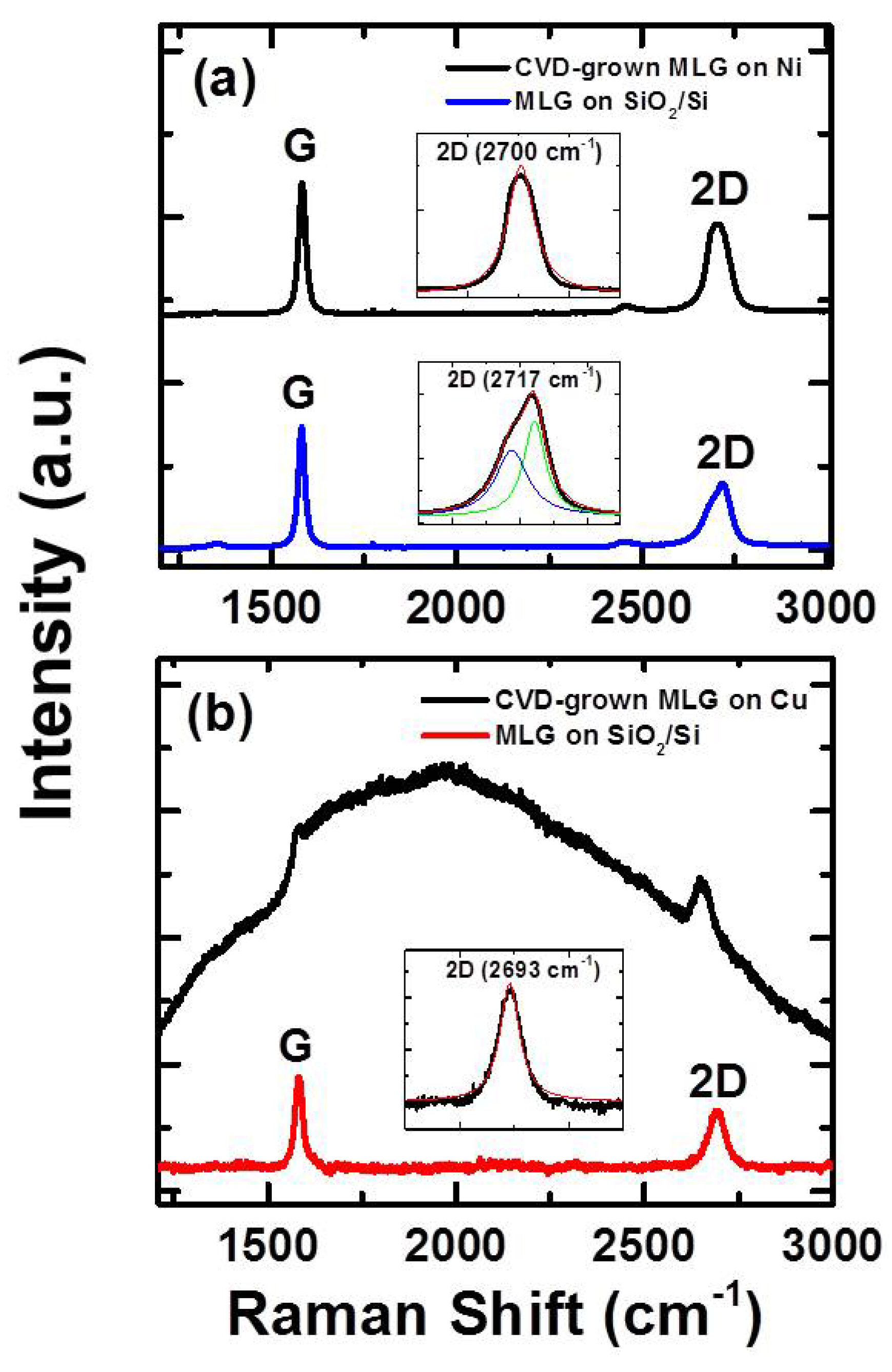
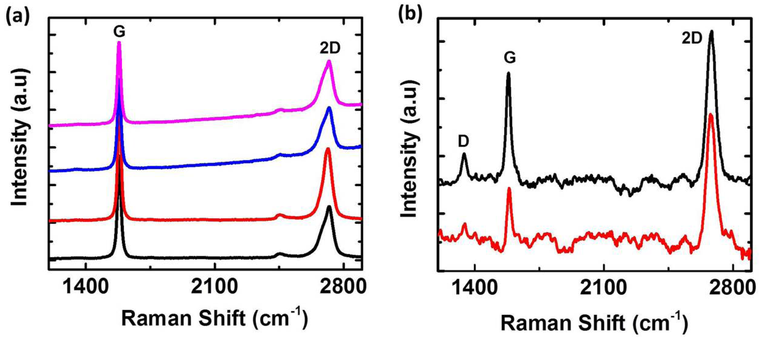
I. Raman Spectroscopic Characterization of Grain Boundaries of CVD-grown Multilayer Graphene (MLG)

Raman spectra have been acquired at room temperature using a Nicolet Almega XR Micro and Macro Raman Analysis System. Excitation laser wavelength has been set to 532 nm (2.33 eV) and the maximum power of 24 mW has been used for the spectroscopy study.
Raman spectra taken from various regions on grain boundaries of MLG-on-Ni are shown in Figure A1(a). No defect (D) peak has been observed (at ~1360 cm−1) in the grain boundary regions of MLG-on-Ni samples. As mentioned in the main text, regions within the grains also exhibit no D peak in the Raman spectrum. Thus, presence of defects can be ruled out in MLG-on-Ni samples. On the contrary, MLG-on-Cu is known to exhibit significant D peak at the grain boundaries [59]. This is consistent with our MLG-on-Cu samples (Figure A1(b), below), which also show D peak at the grain boundaries.
Figure A1. (a) Raman spectra have been taken from various regions on grain boundaries of MLG-on-Ni samples. No defect (D) peak has been observed anywhere; (b) Raman spectra from the grain boundaries of MLG-on-Cu. Clear D peak is present at 1360 cm−1.
Electronics 02 00315 g005
As mentioned in the main text, in case of MLG-on-Ni, fcc and hcp domains of the graphene are possible, depending on the adsorption geometry of the carbon atoms on Ni (111) surface [60]. According to this work, the grain boundaries are often “delaminated” from the Ni substrate and bulge away from the Ni substrate. These features allow matching of fcc and hcp domains by a continuous sheet of graphene, without formation of defects. In our MLG-on-Ni samples we have observed similar bulging features as shown below in Figure A2. This is presumably the reason for not observing D peak in the grain boundaries of our MLG-on-Ni samples.

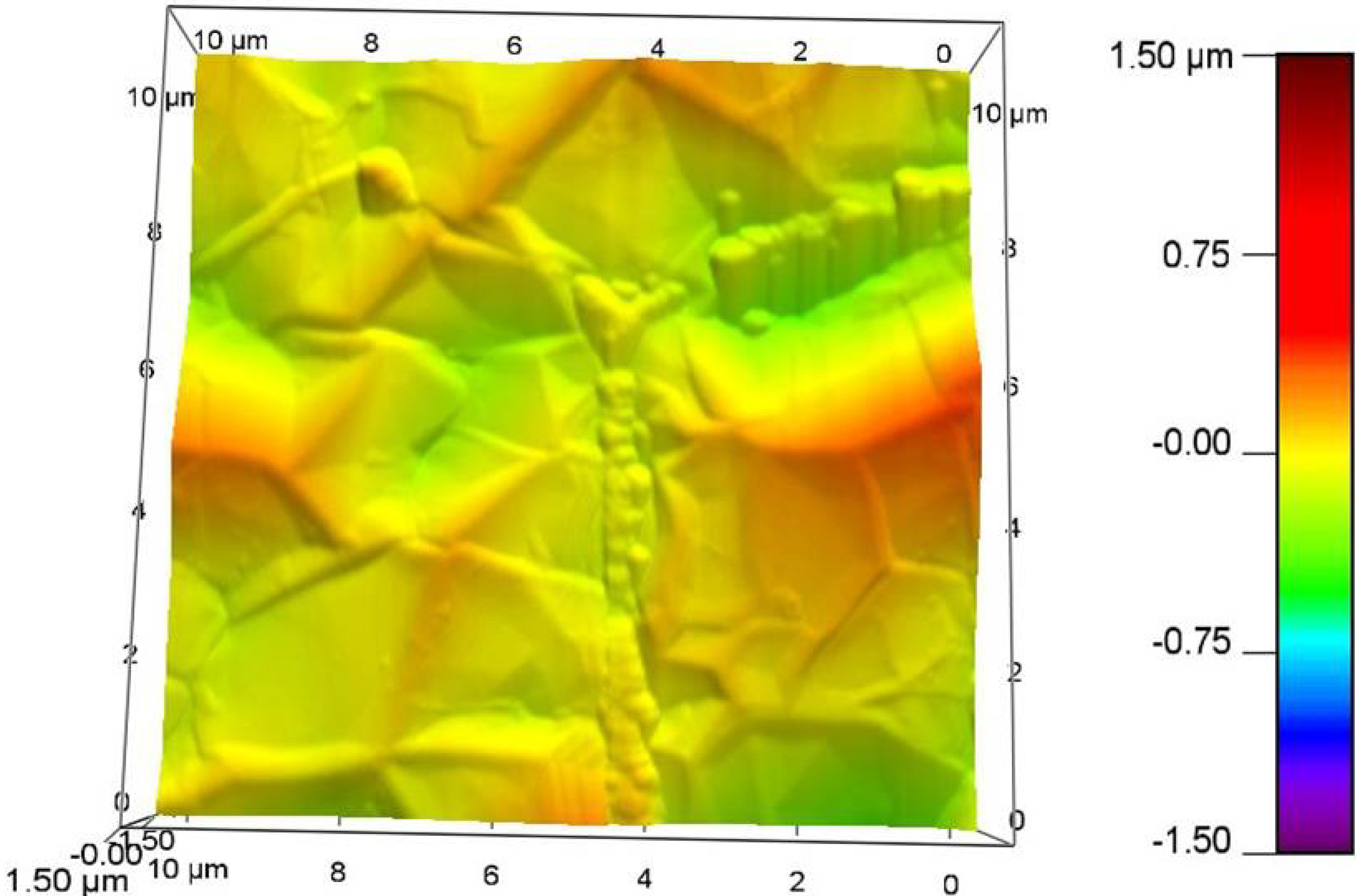
II. AFM Image of Multilayer Graphene on Ni Foil

We used AFM (Asylum Research, MFP-3D) under ambient conditions with a standard tetrahedral silicon tip (Olympus, OMCLAC160TS-W2) located at the end of a silicon cantilever to get surface roughness profile of CVD-grown MLG-on-Ni (Figure A2). Under AC mode, the typical values of force constant, resonant frequency and scan rate were 42 N/m, 300 kHz and 1 Hz respectively. The radius of curvature of the tip is <10 nm.
Figure A2. Atomic Force Microscopic image of CVD-grown MLG-on-Ni
Electronics 02 00315 g006

Conflicts of Interest

The authors declare no conflict of interest.

References

  1. Nickel, J. Magnetoresistance Overview; Hewlett-Packard Laboratories, Technical Publications Department: Palo Alto, CA, USA, 1995. [Google Scholar]
  2. Chappert, C.; Fert, A.; Dau, F.N.V. The emergence of spin electronics in data storage. Nat. Mater. 2007, 6, 813–823. [Google Scholar] [CrossRef]
  3. McGuire, T.; Potter, R. Anisotropic magnetoresistance in ferromagnetic 3d alloys. IEEE Trans. Magn. 1975, 11, 1018–1038. [Google Scholar]
  4. Bergmann, G. Weak localization in thin films: A time-of-flight experiment with conduction electrons. Phys. Rep. 1984, 107, 1–58. [Google Scholar]
  5. Wan, C.; Zhang, X.; Gao, X.; Wang, J.; Tan, X. Geometrical enhancement of low-field magnetoresistance in silicon. Nature 2011, 477, 304–307. [Google Scholar]
  6. Francis, T.L.; Mermer, Ö.; Veeraraghavan, G.; Wohlgenannt, M. Large magnetoresistance at room temperature in semiconducting polymer sandwich devices. New J. Phys. 2004, 6, 185–185. [Google Scholar]
  7. Ramirez, A.P. Colossal magnetoresistance. J. Phys. Condens. Matter 1997, 9, 8171–8199. [Google Scholar]
  8. Biskupski, G. Positive and negative magnetoresistance in the variable-range-hopping regime of doped semiconductors. Philos. Mag. Part B 1992, 65, 723–728. [Google Scholar]
  9. Novoselov, K.S.; Jiang, Z.; Zhang, Y.; Morozov, S.V.; Stormer, H.L.; Zeitler, U.; Maan, J.C.; Boebinger, G.S.; Kim, P.; Geim, A.K. Room-temperature quantum hall effect in graphene. Science 2007, 315, 1379–1379. [Google Scholar] [CrossRef] [Green Version]
  10. Dean, C.R.; Young, A.F.; Cadden-Zimansky, P.; Wang, L.; Ren, H.; Watanabe, K.; Taniguchi, T.; Kim, P.; Hone, J.; Shepard, K.L. Multicomponent fractional quantum hall effect in graphene. Nat. Phys. 2011, 7, 693–696. [Google Scholar]
  11. Kempa, H.; Esquinazi, P.; Kopelevich, Y. Field-induced metal-insulator transition in the c-axis resistivity of graphite. Phys. Rev. B 2002, 65, 241101. [Google Scholar] [CrossRef]
  12. Zhi-Ming, W.; Ding-Yu, X.; Shi-Yuan, Z.; Qing-Yu, X.; VanBael, M.; You-Wei, D. Magnetic-field-induced semimetal-insulator-like transition in highly oriented pyrolitic graphite. Chin. Phys. Lett. 2007, 24, 199–202. [Google Scholar] [CrossRef]
  13. Khveshchenko, D.V. Magnetic-field-induced insulating behavior in highly oriented pyrolitic graphite. Phys. Rev. Lett. 2001, 87, 206401. [Google Scholar] [CrossRef]
  14. Khveshchenko, D.V. Ghost excitonic insulator transition in layered graphite. Phys. Rev. Lett. 2001, 87, 246802. [Google Scholar] [CrossRef]
  15. Kempa, H.; Semmelhack, H.; Esquinazi, P.; Kopelevich, Y. Absence of metal-insulator transition and coherent interlayer transport in oriented graphite in parallel magnetic fields. Solid State Commun. 2003, 125, 1–5. [Google Scholar] [CrossRef]
  16. Liu, Y.; Lew, W.S.; Sun, L. Enhanced weak localization effect in few-layer graphene. Phys. Chem. Chem. Phys. 2011, 13, 20208. [Google Scholar] [CrossRef]
  17. Wu, X.; Li, X.; Song, Z.; Berger, C.; de Heer, W.A. Weak Antilocalization in epitaxial graphene: Evidence for chiral electrons. Phys. Rev. Lett. 2007, 98, 136801. [Google Scholar] [CrossRef]
  18. Tikhonenko, F.V.; Kozikov, A.A.; Savchenko, A.K.; Gorbachev, R.V. Transition between electron localization and antilocalization in graphene. Phys. Rev. Lett. 2009, 103, 226801. [Google Scholar] [CrossRef]
  19. Matis, B.R.; Bulat, F.A.; Friedman, A.L.; Houston, B.H.; Baldwin, J.W. Giant negative magnetoresistance and a transition from strong to weak localization in hydrogenated graphene. Phys. Rev. B 2012, 85, 195437. [Google Scholar]
  20. Liao, Z.-M.; Wu, H.-C.; Kumar, S.; Duesberg, G.S.; Zhou, Y.-B.; Cross, G.L.W.; Shvets, I.V.; Yu, D.-P. Large magnetoresistance in few layer graphene stacks with current perpendicular to plane geometry. Adv. Mater. 2012, 24, 1862–1866. [Google Scholar] [CrossRef]
  21. Friedman, A.L.; Tedesco, J.L.; Campbell, P.M.; Culbertson, J.C.; Aifer, E.; Perkins, F.K.; Myers-Ward, R.L.; Hite, J.K.; Eddy, C.R.; Jernigan, G.G.; et al. Quantum linear magnetoresistance in multilayer epitaxial graphene. Nano Lett. 2010, 10, 3962–3965. [Google Scholar] [CrossRef]
  22. Cobas, E.; Friedman, A.L.; van’t Erve, O.M.J.; Robinson, J.T.; Jonker, B.T. Graphene as a tunnel barrier: Graphene-based magnetic tunnel junctions. Nano Lett. 2012, 12, 3000–3004. [Google Scholar] [CrossRef]
  23. Van’t Erve, O.M.J.; Friedman, A.L.; Cobas, E.; Li, C.H.; Robinson, J.T.; Jonker, B.T. Low-resistance spin injection into silicon using graphene tunnel barriers. Nat. Nanotechnol. 2012, 7, 737–742. [Google Scholar]
  24. Schmidt, G.; Molenkamp, L.W. Spin injection into semiconductors, physics and experiments. Semicond. Sci. Technol. 2002, 17, 310–321. [Google Scholar] [CrossRef]
  25. Dlubak, B.; Martin, M.-B.; Weatherup, R.S.; Yang, H.; Deranlot, C.; Blume, R.; Schloegl, R.; Fert, A.; Anane, A.; Hofmann, S.; et al. Graphene-passivated nickel as an oxidation-resistant electrode for spintronics. ACS Nano 2012, 6, 10930–10934. [Google Scholar]
  26. Friedman, A.L.; Robinson, J.T.; Perkins, F.K.; Campbell, P.M. Extraordinary magnetoresistance in shunted chemical vapor deposition grown graphene devices. Appl. Phys. Lett. 2011, 99, 022108:1–022108:3. [Google Scholar]
  27. Karpan, V.M.; Giovannetti, G.; Khomyakov, P.A.; Talanana, M.; Starikov, A.A.; Zwierzycki, M.; van den Brink, J.; Brocks, G.; Kelly, P.J. Graphite and graphene as perfect spin filters. Phys. Rev. Lett. 2007, 99, 176602. [Google Scholar] [CrossRef]
  28. Karpan, V.M.; Khomyakov, P.A.; Starikov, A.A.; Giovannetti, G.; Zwierzycki, M.; Talanana, M.; Brocks, G.; van den Brink, J.; Kelly, P.J. Theoretical prediction of perfect spin filtering at interfaces between close-packed surfaces of Ni or Co and graphite or graphene. Phys. Rev. B 2008, 78, 195419. [Google Scholar] [CrossRef]
  29. Dedkov, Y.S.; Fonin, M.; Rüdiger, U.; Laubschat, C. Rashba effect in the graphene/Ni(111) system. Phys. Rev. Lett. 2008, 100, 107602. [Google Scholar] [CrossRef]
  30. Wintterlin, J.; Bocquet, M.-L. Graphene on metal surfaces. Surf. Sci. 2009, 603, 1841–1852. [Google Scholar] [CrossRef]
  31. Gong, C.; Lee, G.; Shan, B.; Vogel, E.M.; Wallace, R.M.; Cho, K. First-principles study of metal-graphene interfaces. J. Appl. Phys. 2010, 108, 123711:1–123711:8. [Google Scholar]
  32. Giovannetti, G.; Khomyakov, P.A.; Brocks, G.; Karpan, V.M.; van den Brink, J.; Kelly, P.J. Doping graphene with metal contacts. Phys. Rev. Lett. 2008, 101, 026803. [Google Scholar] [CrossRef]
  33. Xu, Z.; Buehler, M.J. Interface structure and mechanics between graphene and metal substrates: A first-principles study. J. Phys. Condens. Matter 2010, 22, 485301. [Google Scholar] [CrossRef]
  34. Nouchi, R.; Shiraishi, M.; Suzuki, Y. Transfer characteristics in graphene field-effect transistors with Co contacts. Appl. Phys. Lett. 2008, 93, 152104:1–152104:3. [Google Scholar]
  35. Park, N.; Kim, B.-K.; Lee, J.-O.; Kim, J.-J. Influence of metal work function on the position of the Dirac point of graphene field-effect transistors. Appl. Phys. Lett. 2009, 95, 243105:1–243105:3. [Google Scholar]
  36. Zhang, Y.; Gomez, L.; Ishikawa, F.N.; Madaria, A.; Ryu, K.; Wang, C.; Badmaev, A.; Zhou, C. Comparison of graphene growth on single-crystalline and polycrystalline Ni by chemical vapor deposition. J. Phys. Chem. Lett. 2010, 1, 3101–3107. [Google Scholar] [CrossRef]
  37. Yu, Q.; Lian, J.; Siriponglert, S.; Li, H.; Chen, Y.P.; Pei, S.-S. Graphene segregated on Ni surfaces and transferred to insulators. Appl. Phys. Lett. 2008, 93, 113103:1–113103:3. [Google Scholar]
  38. Reina, A.; Jia, X.; Ho, J.; Nezich, D.; Son, H.; Bulovic, V.; Dresselhaus, M.S.; Kong, J. Large area, few-layer graphene films on arbitrary substrates by chemical vapor deposition. Nano Lett. 2008, 9, 30–35. [Google Scholar]
  39. Kim, K.S.; Zhao, Y.; Jang, H.; Lee, S.Y.; Kim, J.M.; Kim, K.S.; Ahn, J.-H.; Kim, P.; Choi, J.-Y.; Hong, B.H. Large-scale pattern growth of graphene films for stretchable transparent electrodes. Nature 2009, 457, 706–710. [Google Scholar] [CrossRef]
  40. Dzemiantsova, L.V.; Karolak, M.; Lofink, F.; Kubetzka, A.; Sachs, B.; von Bergmann, K.; Hankemeier, S.; Wehling, T.O.; Frömter, R.; Oepen, H.P.; Lichtenstein, A.I.; Wiesendanger, R. Multiscale magnetic study of Ni(111) and graphene on Ni(111). Phys. Rev. B 2011, 84, 205431. [Google Scholar] [CrossRef]
  41. Gong, S.J.; Li, Z.Y.; Yang, Z.Q.; Gong, C.; Duan, C.-G.; Chu, J.H. Spintronic properties of graphene films grown on Ni(111) substrate. J. Appl. Phys. 2011, 110, 043704:1–043704:5. [Google Scholar]
  42. Chae, S.J.; Güneş, F.; Kim, K.K.; Kim, E.S.; Han, G.H.; Kim, S.M.; Shin, H.-J.; Yoon, S.-M.; Choi, J.-Y.; Park, M.H.; et al. Synthesis of large-area graphene layers on poly-nickel substrate by chemical vapor deposition: Wrinkle formation. Adv. Mater. 2009, 21, 2328–2333. [Google Scholar] [CrossRef]
  43. Li, X.; Cai, W.; An, J.; Kim, S.; Nah, J.; Yang, D.; Piner, R.; Velamakanni, A.; Jung, I.; Tutuc, E.; et al. Large-Area synthesis of high-quality and uniform graphene films on copper foils. Science 2009, 324, 1312–1314. [Google Scholar] [CrossRef]
  44. Malard, L.M.; Pimenta, M.A.; Dresselhaus, G.; Dresselhaus, M.S. Raman spectroscopy in graphene. Phys. Rep. 2009, 473, 51–87. [Google Scholar] [CrossRef]
  45. Charlier, J.; Eklund, P.; Zhu, J.; Ferrari, A. Electron and Phonon Properties of Graphene: Their Relationship with Carbon Nanotubes. In Carbon Nanotubes; Springer: Berlin/Heidelberg, Germany, 2008; Volume 111, pp. 673–709. [Google Scholar]
  46. Pimenta, M.A.; Dresselhaus, G.; Dresselhaus, M.S.; Cancado, L.G.; Jorio, A.; Saito, R. Studying disorder in graphite-based systems by Raman spectroscopy. Phys. Chem. Chem. Phys. 2007, 9, 1276–1290. [Google Scholar] [CrossRef]
  47. Latil, S.; Meunier, V.; Henrard, L. Massless fermions in multilayer graphitic systems with misoriented layers: Ab initio calculations and experimental fingerprints. Phys. Rev. B 2007, 76, 201402. [Google Scholar] [CrossRef]
  48. Lenski, D.R.; Fuhrer, M.S. Raman and optical characterization of multilayer turbostratic graphene grown via chemical vapor deposition. J. Appl. Phys. 2011, 110, 013720:1–013720:4. [Google Scholar]
  49. Faugeras, C.; Nerrière, A.; Potemski, M.; Mahmood, A.; Dujardin, E.; Berger, C.; de Heer, W.A. Few-layer graphene on SiC, pyrolitic graphite, and graphene: A Raman scattering study. Appl. Phys. Lett. 2008, 92, 011914:1–011914:3. [Google Scholar]
  50. Ni, Z.H.; Wang, Y.Y.; Yu, T.; Shen, Z.X. Raman spectroscopy and imaging of graphene. Nano Res. 2008, 1, 273–291. [Google Scholar] [CrossRef]
  51. Osada, T. Negative interlayer magnetoresistance and zero-mode landau level in multilayer dirac electron systems. J. Phys. Soc. Jpn. 2008, 77, 084711. [Google Scholar] [CrossRef]
  52. Morinari, T.; Tohyama, T. Crossover from positive to negative interlayer magnetoresistance in multilayer massless dirac fermion system with non-vertical interlayer tunneling. J. Phys. Soc. Jpn. 2010, 79, 044708. [Google Scholar] [CrossRef]
  53. Tajima, N.; Sugawara, S.; Kato, R.; Nishio, Y.; Kajita, K. Effect of the zero-mode landau level on interlayer magnetoresistance in multilayer massless dirac fermion systems. Phys. Rev. Lett. 2009, 102, 176403. [Google Scholar]
  54. Tajima, N.; Sato, M.; Sugawara, S.; Kato, R.; Nishio, Y.; Kajita, K. Spin and valley splittings in multilayered massless Dirac fermion system. Phys. Rev. B 2010, 82, 121420. [Google Scholar] [CrossRef]
  55. Bright, A.A. Negative magnetoresistance of pregraphitic carbons. Phys. Rev. B 1979, 20, 5142–5149. [Google Scholar] [CrossRef]
  56. Matsubara, K.; Sugihara, K.; Tsuzuku, T. Electrical resistance in the c direction of graphite. Phys. Rev. B 1990, 41, 969–974. [Google Scholar] [CrossRef]
  57. Venugopal, G.; Jung, M.-H.; Suemitsu, M.; Kim, S.-J. Fabrication of nanoscale three-dimensional graphite stacked-junctions by focused-ion-beam and observation of anomalous transport characteristics. Carbon 2011, 49, 2766–2772. [Google Scholar] [CrossRef]
  58. Acik, M.; Chabal, Y.J. Nature of graphene edges: A review. Jpn. J. Appl. Phys. 2011, 50, 070101. [Google Scholar] [CrossRef]
  59. Yu, Q.; Jauregui, L.A.; Wu, W.; Colby, R.; Tian, J.; Su, Z.; Cao, H.; Liu, Z.; Pandey, D.; Wei, D.; et al. Control and characterization of individual grains and grain boundaries in graphene grown by chemical vapour deposition. Nat. Mater. 2011, 10, 443–449. [Google Scholar] [CrossRef]
  60. Lahiri, J.; Lin, Y.; Bozkurt, P.; Oleynik, I.I.; Batzill, M. An extended defect in graphene as a metallic wire. Nat. Nanotechnol. 2010, 5, 326–329. [Google Scholar] [CrossRef]
  61. Kopelevich, Y.; da Silva, R.R.; Pantoja, J.C.M.; Bratkovsky, A.M. Negative c-axis magnetoresistance in graphite. Phys. Lett. 2010, 374, 4629–4632. [Google Scholar] [CrossRef]

