<?xml version="1.0" encoding="UTF-8"?>
<!DOCTYPE article PUBLIC "-//NLM//DTD Journal Publishing DTD v2.3 20070202//EN" "journalpublishing.dtd">
<article xmlns:mml="http://www.w3.org/1998/Math/MathML" xmlns:xlink="http://www.w3.org/1999/xlink" xml:lang="en" article-type="research-article">
  <front>
    <journal-meta>
      <journal-id journal-id-type="publisher-id">electronics</journal-id>
      <journal-title>Electronics</journal-title>
      <abbrev-journal-title abbrev-type="publisher">Electronics</abbrev-journal-title>
      <abbrev-journal-title abbrev-type="pubmed">Electronics</abbrev-journal-title>
      <issn pub-type="epub">2079-9292</issn>
      <publisher>
        <publisher-name>MDPI</publisher-name>
      </publisher>
    </journal-meta>
    <article-meta>
      <article-id pub-id-type="doi">10.3390/electronics1010023</article-id>
      <article-id pub-id-type="publisher-id">electronics-01-00023</article-id>
      <article-categories>
        <subj-group>
          <subject>Article</subject>
        </subj-group>
      </article-categories>
      <title-group>
        <article-title>Radiation Effects in Carbon Nanoelectronics</article-title>
      </title-group>
      <contrib-group>
        <contrib contrib-type="author">
          <name>
            <surname>Cress</surname>
            <given-names>Cory D.</given-names>
          </name>
          <xref rid="af1-electronics-01-00023" ref-type="aff">1</xref>
          <xref rid="c1-electronics-01-00023" ref-type="corresp">*</xref>
        </contrib>
        <contrib contrib-type="author">
          <name>
            <surname>McMorrow</surname>
            <given-names>Julian J.</given-names>
          </name>
          <xref rid="af2-electronics-01-00023" ref-type="aff">2</xref>
        </contrib>
        <contrib contrib-type="author">
          <name>
            <surname>Robinson</surname>
            <given-names>Jeremy T.</given-names>
          </name>
          <xref rid="af1-electronics-01-00023" ref-type="aff">1</xref>
        </contrib>
        <contrib contrib-type="author">
          <name>
            <surname>Landi</surname>
            <given-names>Brian J.</given-names>
          </name>
          <xref rid="af3-electronics-01-00023" ref-type="aff">3</xref>
        </contrib>
        <contrib contrib-type="author">
          <name>
            <surname>Hubbard</surname>
            <given-names>Seth M.</given-names>
          </name>
          <xref rid="af4-electronics-01-00023" ref-type="aff">4</xref>
        </contrib>
        <contrib contrib-type="author">
          <name>
            <surname>Messenger</surname>
            <given-names>Scott R.</given-names>
          </name>
          <xref rid="af1-electronics-01-00023" ref-type="aff">1</xref>
        </contrib>
      </contrib-group>
      <aff id="af1-electronics-01-00023"><label>1 </label>Electronics Science &amp; Technology Division, U.S. Naval Research Laboratory, Washington, DC 20375, USA</aff>
      <aff id="af2-electronics-01-00023"><label>2 </label>Global Strategies Group (North America) Inc., Crofton, MD 21114, USA</aff>
      <aff id="af3-electronics-01-00023"><label>3 </label>Chemical &amp; Biomedical Engineering Department, Rochester Institute of Technology, Rochester, NY 14623, USA; Email: <email>bjlsps@rit.edu</email></aff>
      <aff id="af4-electronics-01-00023"><label>4 </label>Physics Department, Rochester Institute of Technology, Rochester, NY 14623, USA; Email: <email>smhsps@rit.edu</email></aff>

	  <author-notes>
        <corresp id="c1-electronics-01-00023"><label>*</label> Author to whom correspondence should be addressed; Email: <email>carbon.nanoelectronics@nrl.navy.mil</email>; Tel.: +1-202-767-3462; Fax: +1-202-404-7194.</corresp>
      </author-notes>
      <pub-date pub-type="epub">
        <day>03</day>
        <month>07</month>
        <year>2012</year>
      </pub-date>
      <pub-date pub-type="collection">
        <month>09</month>
        <year>2012</year>
      </pub-date>
      <volume>1</volume>
      <issue>1</issue>
      <fpage>23</fpage>
      <lpage>31</lpage>
      <history>
        <date date-type="received">
          <day>27</day>
          <month>04</month>
          <year>2012</year>
        </date>
        <date date-type="rev-recd">
          <day>15</day>
          <month>06</month>
          <year>2012</year>
        </date>
        <date date-type="accepted">
          <day>19</day>
          <month>06</month>
          <year>2012</year>
        </date>
      </history>
      <permissions>
        <copyright-statement>© 2012 by the authors; licensee MDPI, Basel, Switzerland.</copyright-statement>
        <copyright-year>2012</copyright-year>
        <license xmlns:xlink="http://www.w3.org/1999/xlink" license-type="open-access" xlink:href="http://creativecommons.org/licenses/by/3.0/">
          <p>This article is an open-access article distributed under the terms and conditions of the Creative Commons Attribution license (http://creativecommons.org/licenses/by/3.0/).</p>
        </license>
      </permissions>
      <abstract>
        <p>We experimentally investigate the effects of Co-60 irradiation on the electrical properties of single-walled carbon nanotube and graphene field-effect transistors. We observe significant differences in the radiation response of devices depending on their irradiation environment, and confirm that, under controlled conditions, standard dielectric hardening approaches are applicable to carbon nanoelectronics devices.</p>
      </abstract>
      <kwd-group>
        <kwd>single walled carbon nanotubes</kwd>
        <kwd>graphene</kwd>
        <kwd>total ionizing dose</kwd>
        <kwd>TID</kwd>
        <kwd>radiation hardening</kwd>
        <kwd>FET</kwd>
        <kwd>SWCNT</kwd>
        <kwd>carbon nanoelectronics</kwd>
      </kwd-group>
    </article-meta>
  </front>
  <body>
    <sec sec-type="intro">
      <title>1. Introduction</title>
      <p>The unique properties of carbon nanomaterials, in particular single-walled carbon nanotubes (SWCNTs) and graphene, have garnered much attention due to their potential incorporation into high-performance devices. Recent laboratory-demonstrated threshold frequencies of 80 GHz (SWCNT based) and 100 GHz (graphene based) field-effect transistors (FETs) establish their position among extremely high-mobility materials. Their high mobility and unique ambipolar transport behavior may also prove useful in other analog devices such as power amplifiers, high-frequency mixers, and radio receivers [<xref ref-type="bibr" rid="B1-electronics-01-00023">1</xref>]. It is clear that carbon nanoelectronics will enable, in the near future, leap-ahead technologies to address the needs of terrestrial and space-bound systems. Therefore, it is imperative that the radiation response and methods for radiation hardening be considered in parallel with device development to ensure reliability in harsh environments.</p>
      <p>Many theoretical and experimental studies of SWCNTs, and to a lesser extent graphene, have investigated the effects of ionizing radiation on the crystalline structure of these materials [<xref ref-type="bibr" rid="B2-electronics-01-00023">2</xref>,<xref ref-type="bibr" rid="B3-electronics-01-00023">3</xref>,<xref ref-type="bibr" rid="B4-electronics-01-00023">4</xref>]. The results indicate that ionizing radiation can damage the crystalline lattice by creating defects, although the defect formation probability strongly depends on the energy, mass, and angle of the incident ionizing radiation. Recent studies which monitor the electronic transport properties of carbon-based FETs support these conclusions, that is, a high tolerance to proton irradiation (e.g., SWCNT-FETs [<xref ref-type="bibr" rid="B5-electronics-01-00023">5</xref>,<xref ref-type="bibr" rid="B6-electronics-01-00023">6</xref>], graphene-FETs [<xref ref-type="bibr" rid="B7-electronics-01-00023">7</xref>]) or high-energy photon irradiation (e.g., SWCNT [<xref ref-type="bibr" rid="B8-electronics-01-00023">8</xref>,<xref ref-type="bibr" rid="B9-electronics-01-00023">9</xref>,<xref ref-type="bibr" rid="B10-electronics-01-00023">10</xref>,<xref ref-type="bibr" rid="B11-electronics-01-00023">11</xref>], graphene-FETs [<xref ref-type="bibr" rid="B12-electronics-01-00023">12</xref>,<xref ref-type="bibr" rid="B13-electronics-01-00023">13</xref>,<xref ref-type="bibr" rid="B14-electronics-01-00023">14</xref>]), where the transport properties of the carbon nanostructures are maintained. However, the overall device response to irradiation is mixed. Some studies show enhanced drain currents (e.g., [<xref ref-type="bibr" rid="B7-electronics-01-00023">7</xref>,<xref ref-type="bibr" rid="B10-electronics-01-00023">10</xref>]), or insignificant performance changes [<xref ref-type="bibr" rid="B5-electronics-01-00023">5</xref>], while others report dramatic changes in device behavior including large shifts in threshold voltage [<xref ref-type="bibr" rid="B9-electronics-01-00023">9</xref>]. These assorted results motivate the need for utilizing standardized test structures and controlling the experimental conditions to allow for a systematic evaluation of the radiation response of the materials and devices independent of extrinsic effects.</p>
      <p>In the current study, we illustrate the sensitivities of carbon nanoelectronic devices to total ionizing dose (TID) effects caused by both intrinsic and extrinsic factors. We begin by comparing the effects of TID on a back-gated graphene FET irradiated in vacuum and in air. We then highlight an approach to increasing the performance and radiation tolerance of SWCNT thin-film-transistors (TFTs) using thinned, high-κ gate dielectrics. </p>
    </sec>
    <sec>
      <title>2. Experimental Section</title>
      <p>We employ various device structures to achieve the goals listed above, all of which are processed utilizing the NRL NanoScience Institute cleanroom facilities. The preparation of SWCNT thin films (98% semiconducting-enriched, NanoIntegris, Inc.) and subsequent SWCNT-TFT photolithographic processing closely follow our previously reported procedure found in ref. [<xref ref-type="bibr" rid="B8-electronics-01-00023">8</xref>,<xref ref-type="bibr" rid="B11-electronics-01-00023">11</xref>]. For our back-gated graphene FETs, we grow and transfer graphene films following methods described by Li <italic>et al</italic>. [<xref ref-type="bibr" rid="B15-electronics-01-00023">15</xref>] and use similar photolithographic processing as in Reference [<xref ref-type="bibr" rid="B8-electronics-01-00023">8</xref>]. Briefly, graphene is grown using chemical vapor deposition (CVD) on Cu foils at 1000 °C in a horizontal tube furnace in flowing H<sub>2</sub> and CH<sub>4</sub>. Following growth, graphene is transferred using the following steps: (i) spin-on a protective poly(methyl methacrylate) (PMMA) film; (ii) etch the Cu foil; (iii) transfer the floating PMMA-coated graphene to a substrate of choice; and (iv) remove the PMMA by submersion in an acetone bath. The use of transferred films in the preparation of devices allows us to change the substrate material and structure independently from the carbon nanomaterials. We perform Raman spectroscopy (laser wavelength of 532 nm) of the graphene channel material pre- and post Co-60 irradiation to assess changes in defect concentration in graphene.</p>
      <sec>
        <title>
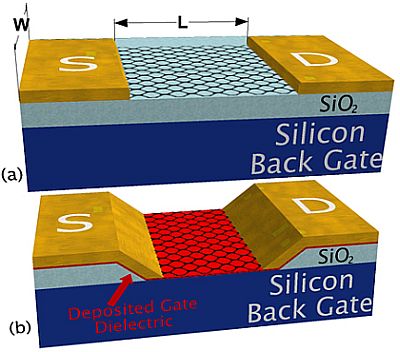
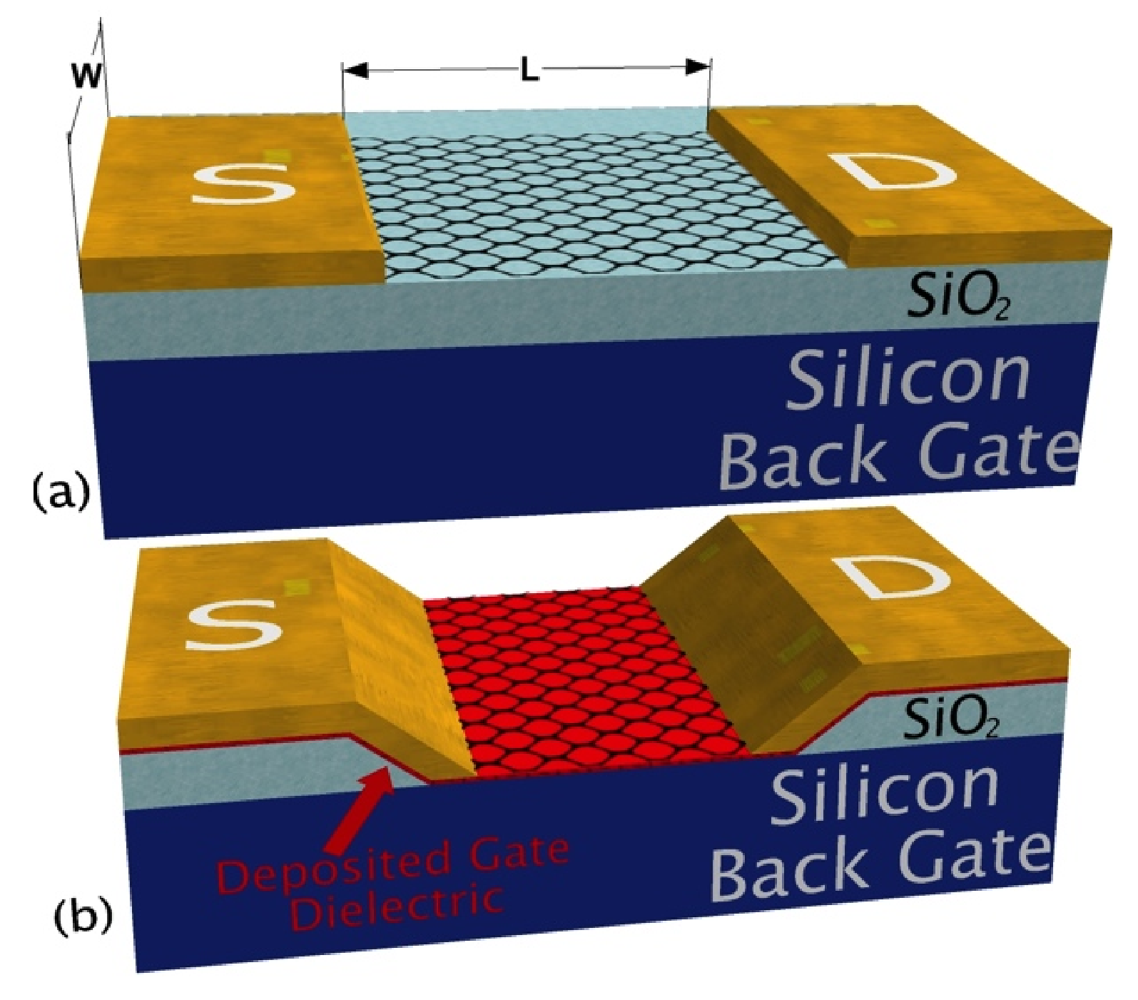
2.1. Back-Gated Device Structures</title>
        <p>The standard back-gated structure depicted in <xref ref-type="fig" rid="electronics-01-00023-f001">Figure 1</xref>a is commonly used to study the electrical transport properties of SWCNTs and graphene. The structure allows for rapid fabrication of devices with variable dimensions. Furthermore, any semiconductor or metal substrate with an insulating dielectric layer may serve as the global back-gate electrode to modulate the Fermi level of the carbon active layer. The devices studied here use thermally grown SiO<sub>2</sub> on p<sup>+</sup>-Si as the starting substrate.</p>
        <fig id="electronics-01-00023-f001" position="anchor">
          <label>Figure 1</label>
          <caption>
            <p>(<bold>a</bold>) Schematic depicting a standard back-gated graphene field-effect transistor (FET) and (<bold>b</bold>) a locally etched back-gated FET structure with a deposited dielectric layer. For the single-walled carbon nanotube (SWCNT)-thin-film-transistors (TFTs), a thin mesh of SWCNTs replaces the graphene film depicted here.</p>
          </caption>
          <graphic xmlns:xlink="http://www.w3.org/1999/xlink" xlink:href="electronics-01-00023-g001.tif"/>
        </fig>
        <p>Though versatile, these back-gated structures are not optimized for high performance since they typically have thick dielectric layers (&gt;1000 Å) resulting in low gate capacitance, and thus, require biases of tens-of-volts to fully saturate or pinch-off the drain current. Furthermore, thick dielectric layers are highly susceptible to radiation induced charge build-up, which is known to cause threshold voltage shifts and increased leakage in metal oxide semiconductor (MOS) devices [<xref ref-type="bibr" rid="B16-electronics-01-00023">16</xref>]. To mitigate these effects, we locally etch the dielectric layer in the active region of the back-gated FET, which is depicted in <xref ref-type="fig" rid="electronics-01-00023-f001">Figure 1</xref>b. We then deposit a gate dielectric material (e.g., Al<sub>2</sub>O<sub>3</sub> or Si<sub>3</sub>N<sub>4</sub>; depicted in red in <xref ref-type="fig" rid="electronics-01-00023-f001">Figure 1</xref>b) over the entire substrate with a thickness controlled by growth. This design feature is important since high quality dielectric layers deposited directly onto SWCNTs or graphene for use as a top gate electrode are still under development. Using the locally etched back-gated (LEBG) structure allows us to maintain the properties of the transferred carbon nanomaterial channel, and have flexibility in the choice and processing performed on the dielectric layer prior to transferring the channel material and fabricating devices.</p>
      </sec>
      <sec>
        <title>2.2. SiO<sub>2</sub> Local Etching</title>
        <p>We pattern the channel regions of the LEBG devices using standard photolithographic procedures. These substrates are etched for 1–3 min in buffered oxide etch (BOE) (7:1 NH<sub>4</sub>F:HF), followed by a short ~1 min rinse in flowing deionized water. This etchant produces smooth hydrogen-terminated Si terraces [<xref ref-type="bibr" rid="B17-electronics-01-00023">17</xref>,<xref ref-type="bibr" rid="B18-electronics-01-00023">18</xref>], thereby providing a controlled surface for subsequent dielectric layer deposition.</p>
      </sec>
      <sec>
        <title>2.3. Si<sub>3</sub>N<sub>4</sub> Plasma Enhanced Chemical Vapor Deposition (PECVD)</title>
        <p>We deposit Si<sub>3</sub>N<sub>4</sub> films on LEBG substrates and BOE etched control wafers for optical and electrical characterization using an Oxford Instruments PlasmaPro™ System 100. Freshly prepared substrates are loaded, pumped to 5 × 10<sup>−6</sup> Torr and preheated to 350 °C for 10 min. Si<sub>3</sub>N<sub>4</sub> deposition proceeds at a pressure of 2 Torr with an N<sub>2</sub> carrier gas, and SiH<sub>4</sub> and NH<sub>4</sub> as the Si and N precursors, respectively. We obtain an index of refraction of 1.97 at 633 nm based on fitted reflectance measurements indicating nearly stoichiometric Si<sub>3</sub>N<sub>4</sub>. Following SWCNT thin-film deposition, annealing the structures in air at 300 °C for 16 h introduces oxygen into the nitride layer transforming it into silicon oxynitride (SiON) with an index of refraction of 1.75 at 633 [<xref ref-type="bibr" rid="B11-electronics-01-00023">11</xref>]. On control samples, we deposit Ti/Au contact pads to perform capacitance and electrical breakdown measurements. For a 23 nm SiON film we obtained an average dielectric constant of <italic>ε<sub>r</sub></italic> = 5.5 at 1 MHz and dc-breakdown fields in excess of 8 MV/cm [<xref ref-type="bibr" rid="B11-electronics-01-00023">11</xref>]. </p>
      </sec>
      <sec>
        <title>2.4. Al<sub>2</sub>O<sub>3</sub> Atomic Layer Deposition (ALD)</title>
        <p>We deposit Al<sub>2</sub>O<sub>3</sub> films on LEBG substrates and BOE etched control wafers for optical and electrical characterization using an Oxford Instruments FlexAL<sup>®</sup> system. In a similar fashion as the Si<sub>3</sub>N<sub>4</sub> we deposit Al<sub>2</sub>O<sub>3</sub> on freshly prepared substrates, which are loaded, pumped, and preheated to 300 °C. The growth proceeds at this temperature as trimethyl aluminum (TMA) the Al precursor and oxygen plasma are alternatingly pulsed into the growth chamber. We deposited Ti/Au contact pads to perform capacitance and electrical breakdown measurements. For a 32 nm Al<sub>2</sub>O<sub>3</sub> film we obtained an average dielectric constant of <italic>ε<sub>r</sub></italic> = 8.3 at 1 MHz and dc-breakdown fields in excess of 10 MV/cm. </p>
      </sec>
    </sec>
    <sec sec-type="results">
      <title>3. Results and Discussion</title>
      <sec>
        <title>3.1. Characterizing Air Sensitivity of Carbon Electronics
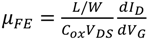
</title>
        <p>We recently observed that the response of SWCNT-TFTs to Co-60 exposure is highly dependent on the local environment of the device during irradiation [<xref ref-type="bibr" rid="B8-electronics-01-00023">8</xref>]. We report here a similar experiment on a standard back-gated graphene FET with a 250 nm SiO<sub>2</sub> gate oxide, channel length of 15 µm, channel width of 60 µm, and a positive gate bias of 5 V during irradiation. <xref ref-type="fig" rid="electronics-01-00023-f002">Figure 2</xref>a illustrates the TID dependent transfer characteristics of the wire bonded standard back-gated graphene FET measured in static vacuum. We measured the pre-irradiation transfer characteristics (black trace labeled 0 krad(Si)) immediately before the first TID exposure (1 krad = 10 Gy). We performed control measurements which yielded constant transfer characteristics for the device held in the sample chamber under static vacuum prior to irradiation. We observe a large shift in the transfer characteristics (towards negative <italic>V<sub>g</sub></italic>) following a TID of 20 krad(Si), which proceeds with further dosing. Following a TID of 40 krad(Si), the Dirac point becomes apparent at <italic>V<sub>g</sub></italic> = 73 V along with the onset of the electron transport for <italic>V<sub>g</sub></italic> &gt; 73 V. These results are consistent with hole trapping in the SiO<sub>2</sub>, which increases the Fermi level closer to mid-gap. Following the initial Co-60 irradiation up to 5 Mrad(Si), we exposed the device to air for 15 m then repeated the experiment with the same device in an air ambient as shown in <xref ref-type="fig" rid="electronics-01-00023-f002">Figure 2</xref>b. During the 15 m repose, the transfer characteristics shift towards positive gate voltage, resulting from room temperature annealing of the radiation-induced trapped charges and due to adsorption of molecular species from the air. Additional irradiation in an air ambient causes the transfer characteristics to shift further towards positive gate bias, the opposite of what we observed when irradiated under vacuum. This indicates that molecular species from the air, namely oxygen and water, overpower the effects of SiO<sub>2</sub> trapped holes and decrease the Fermi level promoting hole doping in the channel [<xref ref-type="bibr" rid="B14-electronics-01-00023">14</xref>].</p>
        <fig id="electronics-01-00023-f002" position="anchor">
          <label>Figure 2</label>
          <caption>
            <p>(<bold>a</bold>) Transfer characteristics of a back-gated graphene-FET with incremental total ionizing dose; (<bold>b</bold>) Transfer characteristics of the same device following 15 min of air exposure (black curve) and with additional total ionizing dose (TID).</p>
          </caption>
          <graphic xmlns:xlink="http://www.w3.org/1999/xlink" xlink:href="electronics-01-00023-g002.tif"/>
        </fig>
        <p>Using the standard long-channel field effect mobility equation: <inline-graphic xmlns:xlink="http://www.w3.org/1999/xlink" xlink:href="electronics-01-00023-i001.tif"/>, where <inline-graphic xmlns:xlink="http://www.w3.org/1999/xlink" xlink:href="electronics-01-00023-i002.tif"/> is the channel length, <inline-graphic xmlns:xlink="http://www.w3.org/1999/xlink" xlink:href="electronics-01-00023-i003.tif"/> is the width, <inline-graphic xmlns:xlink="http://www.w3.org/1999/xlink" xlink:href="electronics-01-00023-i004.tif"/> is the oxide capacitance, <inline-graphic xmlns:xlink="http://www.w3.org/1999/xlink" xlink:href="electronics-01-00023-i005.tif"/> is the drain current, and <inline-graphic xmlns:xlink="http://www.w3.org/1999/xlink" xlink:href="electronics-01-00023-i006.tif"/> is the gate voltage, we calculate the peak <inline-graphic xmlns:xlink="http://www.w3.org/1999/xlink" xlink:href="electronics-01-00023-i007.tif"/> from the transfer curves as plotted verses TID in <xref ref-type="fig" rid="electronics-01-00023-f003">Figure 3</xref>a for the graphene FET irradiated in vacuum and air. When irradiated in vacuum, the hole <inline-graphic xmlns:xlink="http://www.w3.org/1999/xlink" xlink:href="electronics-01-00023-i007.tif"/> initially degrades from 1090 cm<sup>2</sup>/Vs to 980 cm<sup>2</sup>/Vs following a TID of 200 krad(Si), recovers slightly then degrades again reaching a minimum mobility of 896 cm<sup>2</sup>/Vs after a TID of 5 Mrad(Si). During the 15 m repose, the mobility recovers considerably from the low of 896 cm<sup>2</sup>/Vs increasing to 1126 cm<sup>2</sup>/Vs exceeding the pre-irradiation mobility. With increasing TID exposure in air, the mobility decreases to 907 cm<sup>2</sup>/Vs after a TID of 100 krad(Si), then after a brief plateau, degrades to 663 cm<sup>2</sup>/Vs following a total (additional) TID of 5 Mrad(Si) in air. </p>
        
        <p>We also plot the variation in <inline-graphic xmlns:xlink="http://www.w3.org/1999/xlink" xlink:href="electronics-01-00023-i008.tif"/> with TID for the transfer curves measured in vacuum in <xref ref-type="fig" rid="electronics-01-00023-f003">Figure 3</xref>a (lower right <italic>y</italic>-axis). In this figure, <inline-graphic xmlns:xlink="http://www.w3.org/1999/xlink" xlink:href="electronics-01-00023-i008.tif"/> displays non-monotonic behavior that approximately follows that of the mobility (measured in vacuum). The <inline-graphic xmlns:xlink="http://www.w3.org/1999/xlink" xlink:href="electronics-01-00023-i008.tif"/>, for devices of these dimensions, provides a relative measure of the charge inhomogeneity at the graphene-substrate interface resulting from trapped charges in SiO<sub>2</sub> [<xref ref-type="bibr" rid="B19-electronics-01-00023">19</xref>] and adsorbed impurities including oxygen, moisture, and photoresist residues [<xref ref-type="bibr" rid="B20-electronics-01-00023">20</xref>]. The initial decrease in <inline-graphic xmlns:xlink="http://www.w3.org/1999/xlink" xlink:href="electronics-01-00023-i008.tif"/> with TID reflects the increasing trapped charge density and magnitude of charge potential fluctuations (<italic>i.e.</italic>, electron-hole puddles) within the graphene channel. These fluctuations restrict current flow in the graphene channel, which favors transport through regions of unperturbed potential, and is expected to reduce the mobility as we observe. Following a TID of 200–500 krad(Si), the <inline-graphic xmlns:xlink="http://www.w3.org/1999/xlink" xlink:href="electronics-01-00023-i008.tif"/> and <inline-graphic xmlns:xlink="http://www.w3.org/1999/xlink" xlink:href="electronics-01-00023-i007.tif"/> begin to recover. We attribute this behavior to a reorganization of the potential fluctuations in the graphene, potentially resulting in a correlated charge distribution in the SiO<sub>2</sub> [<xref ref-type="bibr" rid="B21-electronics-01-00023">21</xref>] or rearrangement of mobile surface adsorbates, though additional work is needed to confirm this mechanism.
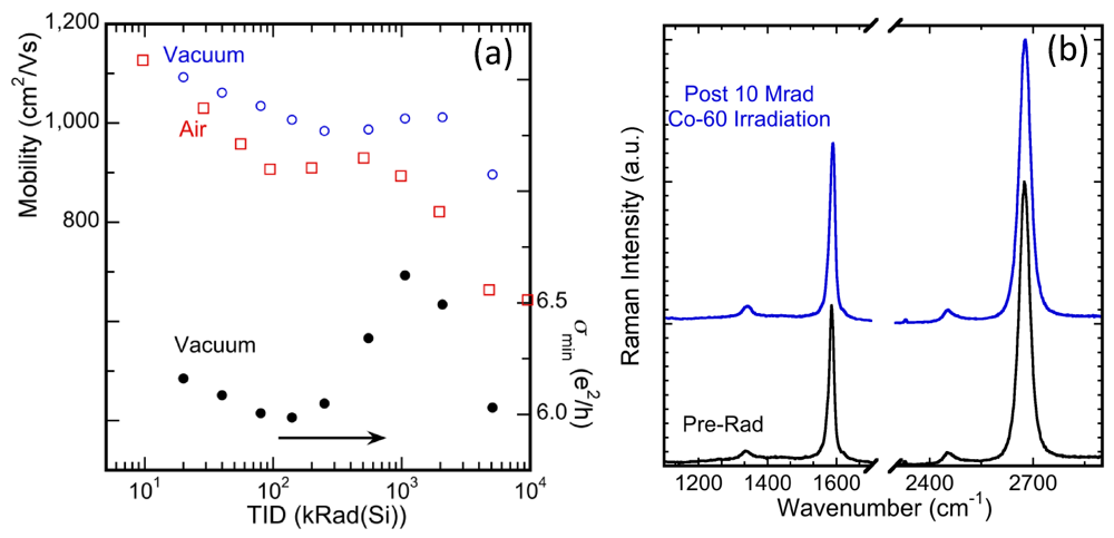
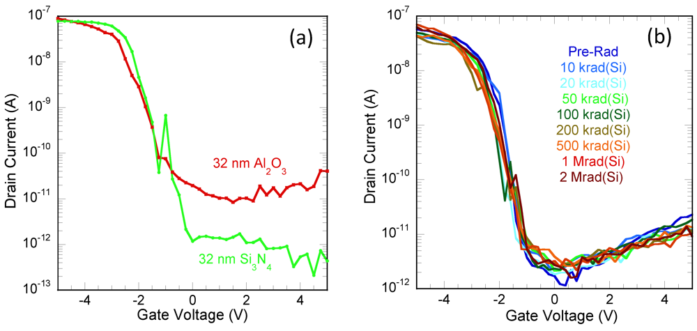
 </p>
        <fig id="electronics-01-00023-f003" position="anchor">
          <label>Figure 3</label>
          <caption>
            <p>(<bold>a</bold>) Field effect mobility as a function of TID for a graphene-FET irradiated in vacuum (blue, open circles) and in air (red, open squares), along with the minimum conductivity (<italic>i.e.</italic>, the conductivity at the Dirac point) for the transfer characteristics measured in vacuum; (<bold>b</bold>) Representative Raman spectra of the graphene FET both pre- and post 10 Mrad(Si) irradiation. </p>
          </caption>
          <graphic xmlns:xlink="http://www.w3.org/1999/xlink" xlink:href="electronics-01-00023-g003.tif"/>
        </fig>
        <p>In <xref ref-type="fig" rid="electronics-01-00023-f003">Figure 3</xref>b we provide characteristic pre- and post 10 Mrad(Si) Co-60 irradiation Raman spectra of the graphene device measured in <xref ref-type="fig" rid="electronics-01-00023-f002">Figure 2</xref>. We measure a 2D-band (2670 cm<sup>−1</sup>) to G-band (1580 cm<sup>−1</sup>) peak intensity ratio of 1.5, which is characteristic of single layer graphene on SiO<sub>2</sub> [<xref ref-type="bibr" rid="B22-electronics-01-00023">22</xref>]. The D-band mode (~1345 cm<sup>−1</sup>) results from disorder in the graphene, potentially arising from defects, edges, wrinkles, or residual PMMA resist, but the relatively low intensity indicates the disorder is minimal. Furthermore, we observe no significant difference in the D-band intensity following irradiation indicating that the changes observed in the graphene FETs due to Co-60 irradiation result from trapped charges in the SiO<sub>2</sub> gate oxide and not due to changes in lattice defect concentration. These results are consistent with our recent study on SWCNTs-TFTs and emphasize the need to control the environmental conditions of carbon electronics, especially when investigating the basic radiation response mechanisms [<xref ref-type="bibr" rid="B8-electronics-01-00023">8</xref>]. Furthermore, the controlled environment results (vacuum data) confirm that, like Si MOS-FETs, carbon electronics are susceptible to the oxide trapped charge effects necessitating the development of radiation-hardened gate dielectrics.</p>
      </sec>
      <sec>
        <title>3.2. SiON and Al<sub>2</sub>O<sub>3</sub> Gate Dielectrics with the Locally Etched Back-Gated Structure (SWCNT-TFTs)</title>
        <p>In <xref ref-type="fig" rid="electronics-01-00023-f004">Figure 4</xref>a we compare the transfer characteristics of two LEBG SWCNT-TFTs with either a 32 nm SiON or a 32 nm Al<sub>2</sub>O<sub>3</sub> gate dielectric layer, 2 µm channel lengths, and 32 µm channel widths. Both devices are representative of the devices with drain current <italic>I<sub>d,on</sub></italic>/<italic>I<sub>d,off</sub></italic> greater than 10<sup>4</sup> (about 20 devices for each gate dielectric). For both dielectric layers, we see a maximum drain current of 1 × 10<sup>−7</sup> A and a consistently lower minimum drain current for the SiON (about 10× lower). The larger off-current may result from the onset of electron transport in the Al<sub>2</sub>O<sub>3</sub> device reflecting the ambipolar transport properties of SWCNTs [<xref ref-type="bibr" rid="B23-electronics-01-00023">23</xref>]. A different level of adsorbed water due to the different surface energies of Al<sub>2</sub>O<sub>3</sub> and Si<sub>3</sub>N<sub>4</sub> may cause this, which is supported by the fact that similar ambipolar behavior is observed in LEBG SWCNT-TFTs with a SiON gate dielectric following vacuum annealing at 125 °C and 1 × 10<sup>−5</sup> Torr (see <xref ref-type="fig" rid="electronics-01-00023-f004">Figure 4</xref>b).</p>
        <fig id="electronics-01-00023-f004" position="anchor">
          <label>Figure 4</label>
          <caption>
            <p>(<bold>a</bold>) Transfer characteristics of SWCNT-TFTs with 32 nm Al<sub>2</sub>O<sub>3</sub> (red) and with 32 nm SiON (green) gate dielectric layers; (<bold>b</bold>) The radiation response of SWCNT-TFT with a 23 nm SiON gate dielectric layer.</p>
          </caption>
          <graphic xmlns:xlink="http://www.w3.org/1999/xlink" xlink:href="electronics-01-00023-g004.tif"/>
        </fig>
        <p>In <xref ref-type="fig" rid="electronics-01-00023-f004">Figure 4</xref>b we investigate the effects of Co-60 irradiation for a LEBG SWCNT-FET with a 23 nm SiON gate oxide and channel length and width of 2 µm and 16 µm, respectively, biased with a 0.25 MV/cm gate field during irradiation. By scaling the gate dielectric material to 23 nm we observe essentially no effect of Co-60 irradiation on the transfer characteristics up to a TID of 2 Mrad(Si). We observe a maximum shift in the threshold voltage of −0.25 V at a TID of 100 krad(Si) after which the transfer characteristics begin to shift back towards positive <italic>V<sub>g</sub></italic> values. The stability in <italic>V<sub>g</sub></italic> results from lower trapped charge accumulation in the thin SiON layer—the thinner layer allows more carriers to escape by tunneling or through field assisted transport [<xref ref-type="bibr" rid="B24-electronics-01-00023">24</xref>]. Furthermore, the trapping characteristics of SiON are distinct from SiO<sub>2</sub> and favor electron trapping over hole trapping [<xref ref-type="bibr" rid="B16-electronics-01-00023">16</xref>]. Therefore, we attribute the positive shift in threshold voltage to electron traps in the SiON [<xref ref-type="bibr" rid="B11-electronics-01-00023">11</xref>], although it is not possible to completely rule out some molecular doping during irradiation in static vacuum conditions. </p>
        <p>The data we have presented here is promising evidence towards hardening carbon nanoelectronics against TID exposure. Therefore, our future investigations are aimed at maintaining the radiation tolerance levels while simultaneously improving device performance and reducing the susceptibility to atmospheric doping effects. </p>
      </sec>
    </sec>
    <sec sec-type="conclusions">
      <title>4. Conclusions</title>
      <p>We have demonstrated the sensitivities of graphene FETs, including shifting Dirac point and mobility degradation, due to TID exposure as well as the compounded effects caused by doping from molecular adsorbates. We observe a correlation between the minimum conductivity, <inline-graphic xmlns:xlink="http://www.w3.org/1999/xlink" xlink:href="electronics-01-00023-i008.tif"/>, and hole mobility, <inline-graphic xmlns:xlink="http://www.w3.org/1999/xlink" xlink:href="electronics-01-00023-i007.tif"/>, both of which vary non-monotonically with increasing TID. We attribute this behavior to an evolving electron-hole puddle distribution, controlled by SiO<sub>2</sub> trapped charges and mobile surface impurities. Using a locally etched back-gate region, we have created a device structure that can leverage standard hardening approaches including the use of alternative dielectric materials and thinner gate dielectric layers. This has led to the demonstration of a SWCNT-TFT which is nearly unaffected by ionizing radiation up to a total dose of 2 Mrad(Si).</p>
    </sec>
  </body>
  <back>
    <ack>
    <title>Acknowledgments</title>
      <p>We acknowledge financial support of this research from the Defense Threat Reduction Agency. We would like to thank H. Hughes, P. McMarr, D. McMorrow for helpful discussions, and A. Friedman for wire bonding. </p>
    </ack>
    <ref-list>
      <title>References</title>
      <ref id="B1-electronics-01-00023">
        <label>1.</label>
        <citation citation-type="journal">
          <person-group person-group-type="author">
            <name>
              <surname>Kocabas</surname>
              <given-names>C.</given-names>
            </name>
            <name>
              <surname>Kim</surname>
              <given-names>H.-S.</given-names>
            </name>
            <name>
              <surname>Banks</surname>
              <given-names>T.</given-names>
            </name>
            <name>
              <surname>Rogers</surname>
              <given-names>J.A.</given-names>
            </name>
            <name>
              <surname>Pesetski</surname>
              <given-names>A.A.</given-names>
            </name>
            <name>
              <surname>Baumgardner</surname>
              <given-names>J.E.</given-names>
            </name>
            <name>
              <surname>Krishnaswamy</surname>
              <given-names>S.V.</given-names>
            </name>
            <name>
              <surname>Zhang</surname>
              <given-names>H.</given-names>
            </name>
          </person-group>
          <article-title>Radio frequency analog electronics based on carbon nanotube transistors</article-title>
          <source>Proc. Natl. Acad. Sci. USA</source>
          <year>2008</year>
          <volume>105</volume>
          <fpage>1405</fpage>
          <lpage>1409</lpage>
        <pub-id pub-id-type="doi">10.1073/pnas.0709734105</pub-id><pub-id pub-id-type="pmid">18227509</pub-id></citation>
      </ref>
      <ref id="B2-electronics-01-00023">
        <label>2.</label>
        <citation citation-type="journal">
          <person-group person-group-type="author">
            <name>
              <surname>Cress</surname>
              <given-names>C.D.</given-names>
            </name>
            <name>
              <surname>Schauerman</surname>
              <given-names>C.M.</given-names>
            </name>
            <name>
              <surname>Landi</surname>
              <given-names>B.J.</given-names>
            </name>
            <name>
              <surname>Messenger</surname>
              <given-names>S.R.</given-names>
            </name>
            <name>
              <surname>Raffaelle</surname>
              <given-names>R.P.</given-names>
            </name>
            <name>
              <surname>Walters</surname>
              <given-names>R.J.</given-names>
            </name>
          </person-group>
          <article-title>Radiation effects in single-walled carbon nanotube papers</article-title>
          <source>J. Appl. Phys.</source>
          <year>2010</year>
          <volume>107</volume>
          <fpage>014316</fpage>
        <pub-id pub-id-type="doi">10.1063/1.3268470</pub-id></citation>
      </ref>
      <ref id="B3-electronics-01-00023">
        <label>3.</label>
        <citation citation-type="journal">
          <person-group person-group-type="author">
            <name>
              <surname>Krasheninnikov</surname>
              <given-names>A.V.</given-names>
            </name>
            <name>
              <surname>Nordlund</surname>
              <given-names>K.</given-names>
            </name>
          </person-group>
          <article-title>Ion and electron irradiation-induced effects in nanostructured materials</article-title>
          <source>J. Appl. Phys.</source>
          <year>2010</year>
          <volume>107</volume>
          <fpage>071301</fpage>
          <pub-id pub-id-type="doi">10.1063/1.3318261</pub-id>
        </citation>
      </ref>
      <ref id="B4-electronics-01-00023">
        <label>4.</label>
        <citation citation-type="journal">
          <person-group person-group-type="author">
            <name>
              <surname>Kaiser</surname>
              <given-names>A.B.</given-names>
            </name>
            <name>
              <surname>Skákalová</surname>
              <given-names>V.</given-names>
            </name>
            <name>
              <surname>Roth</surname>
              <given-names>S.</given-names>
            </name>
          </person-group>
          <article-title>Modelling conduction in carbon nanotube networks with different thickness, chemical treatment and irradiation</article-title>
          <source>Phys. E</source>
          <year>2008</year>
          <volume>40</volume>
          <fpage>2311</fpage>
          <lpage>2318</lpage>
        <pub-id pub-id-type="doi">10.1016/j.physe.2007.10.038</pub-id></citation>
      </ref>
      <ref id="B5-electronics-01-00023">
        <label>5.</label>
        <citation citation-type="journal">
          <person-group person-group-type="author">
            <name>
              <surname>Hong</surname>
              <given-names>W.-K.</given-names>
            </name>
            <name>
              <surname>Lee</surname>
              <given-names>C.</given-names>
            </name>
            <name>
              <surname>Nepal</surname>
              <given-names>D.</given-names>
            </name>
            <name>
              <surname>Geckeler</surname>
              <given-names>K.</given-names>
            </name>
            <name>
              <surname>Shin</surname>
              <given-names>K.</given-names>
            </name>
            <name>
              <surname>Lee</surname>
              <given-names>T.</given-names>
            </name>
          </person-group>
          <article-title>Radiation hardness of the electrical properties of carbon nanotube network field effect transistors under high-energy proton irradiation</article-title>
          <source>Nanotechnology</source>
          <year>2006</year>
          <volume>17</volume>
          <fpage>5675</fpage>
          <lpage>5680</lpage>
          <pub-id pub-id-type="doi">10.1088/0957-4484/17/22/023</pub-id>
        </citation>
      </ref>
      <ref id="B6-electronics-01-00023">
        <label>6.</label>
        <citation citation-type="journal">
          <person-group person-group-type="author">
            <name>
              <surname>Comfort</surname>
              <given-names>E.S.</given-names>
            </name>
            <name>
              <surname>Fishman</surname>
              <given-names>M.</given-names>
            </name>
            <name>
              <surname>Malapanis</surname>
              <given-names>A.</given-names>
            </name>
            <name>
              <surname>Hughes</surname>
              <given-names>H.</given-names>
            </name>
            <name>
              <surname>McMarr</surname>
              <given-names>P.</given-names>
            </name>
            <name>
              <surname>Cress</surname>
              <given-names>C.D.</given-names>
            </name>
            <name>
              <surname>Bakhru</surname>
              <given-names>H.</given-names>
            </name>
            <name>
              <surname>Lee</surname>
              <given-names>J.U.</given-names>
            </name>
          </person-group>
          <article-title>Creation of Individual Defects at Extremely High Proton Fluences in Carbon Nanotube Diodes</article-title>
          <source>Nucl. Sci.</source>
          <year>2011</year>
          <volume>58</volume>
          <fpage>2898</fpage>
          <lpage>2903</lpage>
          <pub-id pub-id-type="doi">10.1109/TNS.2011.2170708</pub-id>
        </citation>
      </ref>
      <ref id="B7-electronics-01-00023">
        <label>7.</label>
        <citation citation-type="journal">
          <person-group person-group-type="author">
            <name>
              <surname>Ko</surname>
              <given-names>G.</given-names>
            </name>
            <name>
              <surname>Kim</surname>
              <given-names>H.Y.</given-names>
            </name>
            <name>
              <surname>Ren</surname>
              <given-names>F.</given-names>
            </name>
            <name>
              <surname>Pearton</surname>
              <given-names>S.J.</given-names>
            </name>
            <name>
              <surname>Kim</surname>
              <given-names>J.</given-names>
            </name>
          </person-group>
          <article-title>Electrical characterization of 5 MeV proton-irradiated few layer graphene</article-title>
          <source>Electrochem. Solid State Lett.</source>
          <year>2010</year>
          <volume>13</volume>
          <fpage>K32</fpage>
          <lpage>K34</lpage>
        <pub-id pub-id-type="doi">10.1149/1.3290777</pub-id></citation>
      </ref>
      <ref id="B8-electronics-01-00023">
        <label>8.</label>
        <citation citation-type="journal">
          <person-group person-group-type="author">
            <name>
              <surname>Cress</surname>
              <given-names>C.D.</given-names>
            </name>
            <name>
              <surname>McMorrow</surname>
              <given-names>J.J.</given-names>
            </name>
            <name>
              <surname>Robinson</surname>
              <given-names>J.T.</given-names>
            </name>
            <name>
              <surname>Friedman</surname>
              <given-names>A.L.</given-names>
            </name>
            <name>
              <surname>Landi</surname>
              <given-names>B.J.</given-names>
            </name>
          </person-group>
          <article-title>Radiation effects in single-walled carbon nanotube thin-film-transistors</article-title>
          <source>IEEE Trans. Nucl. Sci.</source>
          <year>2010</year>
          <volume>57</volume>
          <fpage>3040</fpage>
          <lpage>3045</lpage>
        </citation>
      </ref>
      <ref id="B9-electronics-01-00023">
        <label>9.</label>
        <citation citation-type="journal">
          <person-group person-group-type="author">
            <name>
              <surname>Tang</surname>
              <given-names>X.</given-names>
            </name>
            <name>
              <surname>Yang</surname>
              <given-names>Y.</given-names>
            </name>
            <name>
              <surname>Kim</surname>
              <given-names>W.</given-names>
            </name>
            <name>
              <surname>Wang</surname>
              <given-names>Q.</given-names>
            </name>
            <name>
              <surname>Qi</surname>
              <given-names>P.</given-names>
            </name>
            <name>
              <surname>Dai</surname>
              <given-names>H.</given-names>
            </name>
          </person-group>
          <article-title>Measurement of ionizing radiation using carbon nanotube field effect transistor</article-title>
          <source>Phys. Med. Biol.</source>
          <year>2005</year>
          <volume>50</volume>
          <fpage>N23</fpage>
          <lpage>N31</lpage>
          <pub-id pub-id-type="doi">10.1088/0031-9155/50/3/N02</pub-id>
        </citation>
      </ref>
      <ref id="B10-electronics-01-00023">
        <label>10.</label>
        <citation citation-type="journal">
          <person-group person-group-type="author">
            <name>
              <surname>Vitusevich</surname>
              <given-names>S.A.</given-names>
            </name>
            <name>
              <surname>Sydoruk</surname>
              <given-names>V.A.</given-names>
            </name>
            <name>
              <surname>Petrychuk</surname>
              <given-names>M.V.</given-names>
            </name>
            <name>
              <surname>Danilchenko</surname>
              <given-names>B.A.</given-names>
            </name>
            <name>
              <surname>Klein</surname>
              <given-names>N.</given-names>
            </name>
            <name>
              <surname>Offenhäusser</surname>
              <given-names>A.</given-names>
            </name>
            <name>
              <surname>Ural</surname>
              <given-names>A.</given-names>
            </name>
            <name>
              <surname>Bosman</surname>
              <given-names>G.</given-names>
            </name>
          </person-group>
          <article-title>Transport properties of single-walled carbon nanotube transistors after gamma radiation treatment</article-title>
          <source>J. Appl. Phys.</source>
          <year>2010</year>
          <volume>107</volume>
          <fpage>063701</fpage>
        <pub-id pub-id-type="doi">10.1063/1.3340977</pub-id></citation>
      </ref>
      <ref id="B11-electronics-01-00023">
        <label>11.</label>
        <citation citation-type="journal">
          <person-group person-group-type="author">
            <name>
              <surname>Cress</surname>
              <given-names>C.D.</given-names>
            </name>
            <name>
              <surname>McMorrow</surname>
              <given-names>J.J.</given-names>
            </name>
            <name>
              <surname>Robinson</surname>
              <given-names>J.T.</given-names>
            </name>
            <name>
              <surname>Friedman</surname>
              <given-names>A.L.</given-names>
            </name>
            <name>
              <surname>Hughes</surname>
              <given-names>H.L.</given-names>
            </name>
            <name>
              <surname>Weaver</surname>
              <given-names>B.D.</given-names>
            </name>
            <name>
              <surname>Landi</surname>
              <given-names>B.J.</given-names>
            </name>
          </person-group>
          <article-title>Total ionizing dose-hardened carbon nanotube thin-film transistors with silicon oxynitride gate dielectrics</article-title>
          <source>MRS Commun.</source>
          <year>2011</year>
          <volume>1</volume>
          <fpage>27</fpage>
          <lpage>31</lpage>
          <pub-id pub-id-type="doi">10.1557/mrc.2011.10</pub-id>
        </citation>
      </ref>
      <ref id="B12-electronics-01-00023">
        <label>12.</label>
        <citation citation-type="confproc">
          <person-group person-group-type="author">
            <name>
              <surname>Cress</surname>
              <given-names>C.D.</given-names>
            </name>
            <name>
              <surname>McMorrow</surname>
              <given-names>J.J.</given-names>
            </name>
            <name>
              <surname>Robinson</surname>
              <given-names>J.T.</given-names>
            </name>
            <name>
              <surname>Landi</surname>
              <given-names>B.J.</given-names>
            </name>
            <name>
              <surname>Hubbard</surname>
              <given-names>S.M.</given-names>
            </name>
            <name>
              <surname>Messenger</surname>
              <given-names>S.R.</given-names>
            </name>
          </person-group>
          <article-title>Radiation-hardening of carbon nanoelectronics</article-title>
          <source>Proceedings of the Government Microcircuit Applications and Critical Technologies Conference</source>
          <conf-loc>Orlando, FL, USA</conf-loc>
          <conf-date>2011</conf-date>
          <fpage>1</fpage>
          <lpage>5</lpage>
        </citation>
      </ref>
      <ref id="B13-electronics-01-00023">
        <label>13.</label>
        <citation citation-type="journal">
          <person-group person-group-type="author">
            <name>
              <surname>Schrimpf</surname>
              <given-names>R.D.</given-names>
            </name>
            <name>
              <surname>Fleetwood</surname>
              <given-names>D.M.</given-names>
            </name>
            <name>
              <surname>Alles</surname>
              <given-names>M.L.</given-names>
            </name>
            <name>
              <surname>Reed</surname>
              <given-names>R.A.</given-names>
            </name>
            <name>
              <surname>Lucovsky</surname>
              <given-names>G.</given-names>
            </name>
            <name>
              <surname>Pantelides</surname>
              <given-names>S.T.</given-names>
            </name>
          </person-group>
          <article-title>Radiation effects in new materials for nano-devices</article-title>
          <source>Microelectron. Eng.</source>
          <year>2011</year>
          <volume>88</volume>
          <fpage>1</fpage>
          <lpage>6</lpage>
        <pub-id pub-id-type="doi">10.1016/j.mee.2010.07.031</pub-id></citation>
      </ref>
      <ref id="B14-electronics-01-00023">
        <label>14.</label>
        <citation citation-type="journal">
          <person-group person-group-type="author">
            <name>
              <surname>Zhang</surname>
              <given-names>E.X.</given-names>
            </name>
            <name>
              <surname>Newaz</surname>
              <given-names>A.K.M.</given-names>
            </name>
            <name>
              <surname>Wang</surname>
              <given-names>B.</given-names>
            </name>
            <name>
              <surname>Bhandaru</surname>
              <given-names>S.</given-names>
            </name>
            <name>
              <surname>Zhang</surname>
              <given-names>C.X.</given-names>
            </name>
            <name>
              <surname>Fleetwood</surname>
              <given-names>D.M.</given-names>
            </name>
            <name>
              <surname>Bolotin</surname>
              <given-names>K.I.</given-names>
            </name>
            <name>
              <surname>Pantelides</surname>
              <given-names>S.T.</given-names>
            </name>
            <name>
              <surname>Alles</surname>
              <given-names>M.L.</given-names>
            </name>
            <name>
              <surname>Schrimpf</surname>
              <given-names>R.D.</given-names>
            </name>
            <etal/>
          </person-group>
          <article-title>Low-energy X-ray and  ozone-exposure induced defect formation in graphene materials and devices</article-title>
          <source>IEEE Trans. Nucl. Sci.</source>
          <year>2011</year>
          <volume>58</volume>
          <fpage>2961</fpage>
          <lpage>2967</lpage>
        <pub-id pub-id-type="doi">10.1109/TNS.2011.2167519</pub-id></citation>
      </ref>
      <ref id="B15-electronics-01-00023">
        <label>15.</label>
        <citation citation-type="journal">
          <person-group person-group-type="author">
            <name>
              <surname>Li</surname>
              <given-names>X.</given-names>
            </name>
            <name>
              <surname>Zhu</surname>
              <given-names>Y.</given-names>
            </name>
            <name>
              <surname>Cai</surname>
              <given-names>W.</given-names>
            </name>
            <name>
              <surname>Borysiak</surname>
              <given-names>M.</given-names>
            </name>
            <name>
              <surname>Han</surname>
              <given-names>B.</given-names>
            </name>
            <name>
              <surname>Chen</surname>
              <given-names>D.</given-names>
            </name>
            <name>
              <surname>Piner</surname>
              <given-names>R.</given-names>
            </name>
            <name>
              <surname>Colomba</surname>
              <given-names>L.</given-names>
            </name>
            <name>
              <surname>Ruoff</surname>
              <given-names>R.</given-names>
            </name>
          </person-group>
          <article-title>Transfer of large-area graphene films for high-performance transparent conductive electrodes</article-title>
          <source>Nano Lett.</source>
          <year>2009</year>
          <volume>9</volume>
          <fpage>4359</fpage>
          <lpage>4363</lpage>
        <pub-id pub-id-type="doi">10.1021/nl902623y</pub-id><pub-id pub-id-type="pmid">19845330</pub-id></citation>
      </ref>
      <ref id="B16-electronics-01-00023">
        <label>16.</label>
        <citation citation-type="book">
          <person-group person-group-type="author">
            <name>
              <surname>Oldham</surname>
              <given-names>T.</given-names>
            </name>
          </person-group>
          <source>Ionizing Radiation Effects in MOS Oxides</source>
          <publisher-name>World Scientific</publisher-name>
          <publisher-loc>Singapore</publisher-loc>
          <year>1999</year>
        </citation>
      </ref>
      <ref id="B17-electronics-01-00023">
        <label>17.</label>
        <citation citation-type="journal">
          <person-group person-group-type="author">
            <name>
              <surname>Le Thanh</surname>
              <given-names>V.</given-names>
            </name>
            <name>
              <surname>Bouchier</surname>
              <given-names>D.</given-names>
            </name>
            <name>
              <surname>Débarre</surname>
              <given-names>D.</given-names>
            </name>
          </person-group>
          <article-title>Fabrication of SiGe quantum dots on a Si(100) surface</article-title>
          <source>Phys. Rev. B</source>
          <year>1997</year>
          <volume>56</volume>
          <fpage>10505</fpage>
          <lpage>10510</lpage>
        <pub-id pub-id-type="doi">10.1103/PhysRevB.56.10505</pub-id></citation>
      </ref>
      <ref id="B18-electronics-01-00023">
        <label>18.</label>
        <citation citation-type="journal">
          <person-group person-group-type="author">
            <name>
              <surname>Pietsch</surname>
              <given-names>G.J.</given-names>
            </name>
          </person-group>
          <article-title>Hydrogen on Si: Ubiquitous surface termination after wet-chemical processing</article-title>
          <source>Appl. Phys. A</source>
          <year>1995</year>
          <volume>60</volume>
          <fpage>347</fpage>
          <lpage>363</lpage>
          <pub-id pub-id-type="doi">10.1007/BF01538334</pub-id>
        </citation>
      </ref>
      <ref id="B19-electronics-01-00023">
        <label>19.</label>
        <citation citation-type="journal">
          <person-group person-group-type="author">
            <name>
              <surname>Sui</surname>
              <given-names>Y.</given-names>
            </name>
            <name>
              <surname>Low</surname>
              <given-names>T.</given-names>
            </name>
            <name>
              <surname>Lundstrom</surname>
              <given-names>M.</given-names>
            </name>
            <name>
              <surname>Appenzeller</surname>
              <given-names>J.</given-names>
            </name>
          </person-group>
          <article-title>Signatures of disorder in the minimum conductivity of graphene</article-title>
          <source>Nano Lett.</source>
          <year>2011</year>
          <volume>11</volume>
          <fpage>1319</fpage>
          <lpage>1322</lpage>
          <pub-id pub-id-type="doi">10.1021/nl104399z</pub-id>
        </citation>
      </ref>
      <ref id="B20-electronics-01-00023">
        <label>20.</label>
        <citation citation-type="journal">
          <person-group person-group-type="author">
            <name>
              <surname>Adam</surname>
              <given-names>S.</given-names>
            </name>
            <name>
              <surname>Hwang</surname>
              <given-names>E.H.</given-names>
            </name>
            <name>
              <surname>Galitski</surname>
              <given-names>V.M.</given-names>
            </name>
            <name>
              <surname>Das Sarma</surname>
              <given-names>S.</given-names>
            </name>
          </person-group>
          <article-title>A self-consistent theory for graphene transport</article-title>
          <source>Proc. Natl. Acad. Sci. USA</source>
          <year>2007</year>
          <volume>104</volume>
          <fpage>18392</fpage>
          <lpage>18397</lpage>
        <pub-id pub-id-type="doi">10.1073/pnas.0704772104</pub-id><pub-id pub-id-type="pmid">18003926</pub-id></citation>
      </ref>
      <ref id="B21-electronics-01-00023">
        <label>21.</label>
        <citation citation-type="journal">
          <person-group person-group-type="author">
            <name>
              <surname>Yan</surname>
              <given-names>J.</given-names>
            </name>
            <name>
              <surname>Fuhrer</surname>
              <given-names>M.</given-names>
            </name>
          </person-group>
          <article-title>Correlated charged impurity scattering in graphene</article-title>
          <source>Phys. Rev. Lett.</source>
          <year>2011</year>
          <volume>107</volume>
          <fpage>206601</fpage>
          <pub-id pub-id-type="doi">10.1103/PhysRevLett.107.206601</pub-id>
        </citation>
      </ref>
      <ref id="B22-electronics-01-00023">
        <label>22.</label>
        <citation citation-type="journal">
          <person-group person-group-type="author">
            <name>
              <surname>Li</surname>
              <given-names>X.</given-names>
            </name>
            <name>
              <surname>Cai</surname>
              <given-names>W.</given-names>
            </name>
            <name>
              <surname>An</surname>
              <given-names>J.</given-names>
            </name>
            <name>
              <surname>Kim</surname>
              <given-names>S.</given-names>
            </name>
            <name>
              <surname>Nah</surname>
              <given-names>J.</given-names>
            </name>
            <name>
              <surname>Yang</surname>
              <given-names>D.</given-names>
            </name>
            <name>
              <surname>Piner</surname>
              <given-names>R.</given-names>
            </name>
            <name>
              <surname>Velamakanni</surname>
              <given-names>A.</given-names>
            </name>
            <name>
              <surname>Jung</surname>
              <given-names>I.</given-names>
            </name>
            <name>
              <surname>Tutuc</surname>
              <given-names>E.</given-names>
            </name>
            <etal/>
          </person-group>
          <article-title>Large-area synthesis of high-quality and uniform graphene films on copper foils</article-title>
          <source>Science</source>
          <year>2009</year>
          <volume>324</volume>
          <fpage>1312</fpage>
          <lpage>1314</lpage>
        <pub-id pub-id-type="doi">10.1126/science.1171245</pub-id><pub-id pub-id-type="pmid">19423775</pub-id></citation>
      </ref>
      <ref id="B23-electronics-01-00023">
        <label>23.</label>
        <citation citation-type="journal">
          <person-group person-group-type="author">
            <name>
              <surname>Javey</surname>
              <given-names>A.</given-names>
            </name>
            <name>
              <surname>Shim</surname>
              <given-names>M.</given-names>
            </name>
            <name>
              <surname>Dai</surname>
              <given-names>H.</given-names>
            </name>
          </person-group>
          <article-title>Electrical properties and devices of large-diameter single-walled carbon nanotubes</article-title>
          <source>Appl. Phys. Lett.</source>
          <year>2002</year>
          <volume>80</volume>
          <fpage>1064</fpage>
          <pub-id pub-id-type="doi">10.1063/1.1448850</pub-id>
        </citation>
      </ref>
      <ref id="B24-electronics-01-00023">
        <label>24.</label>
        <citation citation-type="journal">
          <person-group person-group-type="author">
            <name>
              <surname>Saks</surname>
              <given-names>N.</given-names>
            </name>
            <name>
              <surname>Ancona</surname>
              <given-names>M.</given-names>
            </name>
            <name>
              <surname>Modolo</surname>
              <given-names>J.</given-names>
            </name>
          </person-group>
          <article-title>Radiation Effects in MOS Capacitors with Very Thin Oxides at 80 °K</article-title>
          <source>IEEE Trans. Nucl. Sci.</source>
          <year>1984</year>
          <volume>31</volume>
          <fpage>1249</fpage>
          <lpage>1255</lpage>
          <pub-id pub-id-type="doi">10.1109/TNS.1984.4333491</pub-id>
        </citation>
      </ref>
    </ref-list>
  </back>
</article>
