Novel Approaches for Efficient Delay-Insensitive Communication


Institute for Computer Engineering, TU Wien, 1040 Vienna, Austria
*
Author to whom correspondence should be addressed.
J. Low Power Electron. Appl. 2019, 9(2), 16; https://doi.org/10.3390/jlpea9020016
Submission received: 7 December 2018
/
Revised: 17 March 2019
/
Accepted: 29 March 2019
/
Published: 6 April 2019
(This article belongs to the Special Issue Selected Papers from the 24th IEEE International Symposium on Asynchronous Circuits and Systems - ASYNC 2018)
Abstract
:The increasing complexity and modularity of contemporary systems, paired with increasing parameter variabilities, makes the availability of flexible and robust, yet efficient, module-level interconnections instrumental. Delay-insensitive codes are very attractive in this context. There is considerable literature on this topic that classifies delay-insensitive communication channels according to the protocols (return-to-zero versus non-return-to-zero) and with respect to the codes (constant-weight versus systematic), with each solution having its specific pros and cons. From a higher abstraction, however, these protocols and codes represent corner cases of a more comprehensive solution space, and an exploration of this space promises to yield interesting new approaches. This is exactly what we do in this paper. More specifically, we present a novel coding scheme that combines the benefits of constant-weight codes, namely simple completion detection, with those of systematic codes, namely zero-effort decoding. We elaborate an approach for composing efficient “Partially Systematic Constant Weight” codes for a given data word length. In addition, we explore cost-efficient and orphan-free implementations of completion detectors for both, as well as suitable encoders and decoders. With respect to the protocols, we investigate the use of multiple spacers in return-to-zero protocols. We show that having a choice between multiple spacers can be beneficial with respect to energy efficiency. Alternatively, the freedom to choose one of multiple spacers can be leveraged to transfer information, thus turning the original return-to-zero protocol into a (very basic version of a) non-return-to-zero protocol. Again, this intermediate solution can combine benefits from both extremes. For all proposed solutions we provide quantitative comparisons that cover the whole relevant design space. In particular, we derive coding efficiency, power efficiency, as well as area effort for pipelined and non-pipelined communication channels. This not only gives evidence for the benefits and limitations of the presented novel schemes—our hope is that this paper can serve as a reference for designers seeking an optimized delay-insensitive code/protocol/implementation for their specific application.
1. Introduction
Compared to synchronous approaches, asynchronous delay-insensitive (DI) communication links have very desirable properties with respect to their robustness against timing variations and delay assumptions required to implement them. This makes them especially interesting as a form of system-level intra-chip or inter-chip connection, particularly in the context of Globally Asynchronous Locally Synchronous (GALS) systems [1]. Hence, in this paper we seek to explore the design space of how such links can be implemented and provide new insights into key components and communication protocols involved.
In many contemporary applications, energy efficiency of semi-conductors is a major concern. It is well understood that communication links between function blocks (within an SoC, or on a PCB) are a significant contributor to the overall power consumption of a system, due to the relatively high capacitances involved. In this context, synchronous communication has some disadvantages due to the high transition rate of the clock line. Moreover, delay mismatch (skew) among the different wires of the communication link is problematic. This also holds true for those asynchronous approaches that employ some kind of “valid signal” for a bundle of data wires. With ever-increasing process/voltage/temperature (PVT) variations these issues steadily gather more relevance. DI communication elegantly overcomes these problems: Here the data encoding is chosen such that the receiver can recognize when a code word is complete (i.e., all wires made their final transitions)—in the absence of an accompanying clock or valid signal, and even in the presence of arbitrary skew on the transmission link. Such links have been successfully employed in many applications, such as Spinnaker [2,3], or Chain [4].
However, special DI codes must be used to encode the data being transmitted. These codes are required to allow the receiver to use a completion detector (CD) for deciding whether the input bit pattern is a valid (i.e., complete) code word, or if further transitions must be awaited. If a code word is complete, the receiver asserts the acknowledgment () signal (an additional wire from receiver to sender) to notify the sender that the code word has been consumed. One drawback of DI codes is that they are generally not well-suited for data processing. Even for codes where this is comparatively easy to implement, a considerable hardware (i.e., chip area) overhead must be expected. Hence for our analysis we assume that the transmitter and receiver operate on binary coded data, in particular we consider asynchronous bundled data (BD) channels. Consequently, we will also discuss circuits that convert binary coded data (i.e., a data word) to a DI code word, which we refer to as encoders, as well as circuits that perform the reverse operation, called decoders. Figure 1 shows where these components as well as the CDs reside in the DI link.
A fundamental problem of DI interconnection is to find the right balance between efficiency of the DI code and protocol on the one hand, and the implementation complexity on the other (i.e., the area overhead for encoders, decoders, and CDs). In this context, efficiency refers to the number of data bits a code word of a given length can hold as well as to the number of bus transitions it requires for transmission. Generally, complex codes and protocols have a better efficiency but are more costly to implement.
In this work we investigate and compare constant weight (i.e., m-of-n) and Berger codes [5]. In general, Berger codes excel because of their simple encoding and the complete absence of a decoder, while, unfortunately, their CDs tend to become complex and difficult to realize in a complete DI way (i.e., without timing assumptions). Constant-weight codes, on the other hand, often provide higher coding efficiency and facilitate completion detection with significantly lower efforts, but incur a higher penalty for encoding and decoding. The reason for the high overhead is that constant-weight codes are not systematic, i.e., the mapping between data words and code words is not predetermined by the code itself (in contrast to Berger codes). However, this mapping strongly impacts the implementation overhead, and even optimizing the implementation for a given mapping is non-trivial as was already tackled in [6].
Consequently, the first contribution of this paper is a code word mapping approach for constant-weight codes, which divides the code words into a systematic and a non-systematic part. We refer to this mapping scheme as Partially Systematic Constant-Weight Codes (PSCWCs). Our presumption is that the systematic part will simplify the encoding and decoding process. Building on our previous work from [7] we show that this approach indeed yields very regular mappings with reoccurring sub-codes for the non-systematic part, which allows for efficient encoder and decoder circuits. Although the method is not fully generalized, we carefully explore the design space relevant for DI communication links.
The second contribution we present in this work is a new class of DI protocols, which bridge the two “classical” asynchronous approaches—that is the return-to-zero and the non-return-to-zero protocol. With these hybrid protocols, whose concept we had already introduced in [8], we are able to show that there is a whole spectrum of DI communication schemes, each with different use cases, complexity, advantages and disadvantages.
Furthermore, we provide, based on some prior work [9,10,11], improved CDs for the m-of-n and Berger code classes that work with the return-to-zero as well as the new hybrid protocols. In our construction approach, we carefully avoid so-called orphan transitions, which compromise the timing model of the CD circuits and which are not fully avoided by current state-of-the-art solutions.
Finally, we present an extensive case study were we systematically analyze all techniques presented in this paper. We not only investigate the area overhead for encoders, decoders, and CDs for all codes and protocols discussed in this paper but also consider the overall implementation costs of complete DI communication links for the model-architectures we use in this context. In addition, we perform a systematic analysis of the performance implications of the different approaches. This analysis provides useful insights into the advantages and disadvantages of the individual approaches for different use cases.
The paper is structured as follows. First Section 2 will give a brief overview of DI codes and communication protocols and introduce important notation and definitions used throughout the paper. The PSCWCs, hybrid protocols and completion detectors are discussed in Section 3, Section 4 and Section 5, respectively. Section 6 then provides example implementations for all protocols discussed in this paper, while Section 7 presents an overall comparison of all approaches. Finally, Section 8 concludes the paper.
2. Asynchronous Delay-Insensitive Communication
In contrast to the rigid time-driven regime of synchronous design, asynchronous circuits always use some form of closed-loop handshaking protocol to control the data transfer between storage elements (e.g., pipeline stages). This is actually the key for obtaining tolerance against PVT variations.
As shown in Figure 2 this handshake (usually) involves two signals, request () and acknowledgment () line. The rising edge of the signal is typically used as an indicator by the source to notify the sink that new data is available. The sink then uses the signal to inform the source that it has received the data and that new data can be transmitted. This explanation assumes push channels. In pull channels the meaning of the request and acknowledgment signals are reversed, see [12] for a more detailed discussion. However, the rest of the paper will only consider push channels.
At this point we must address the difference between 2-phase and 4-phase protocols, which is also shown in Figure 2. In the former case, every transition of and conveys actual information. Hence every handshaking cycle (labeled Events in the figure) consists of two transitions. 4-phase protocols, on the other side, always entail a reset phase where both signals return to zero again. Please note that there is an immanent race condition between the request signal and the data that is being transmitted. It must be guaranteed that the request reaches the sink only after the data is stable at its input. In the so-called BD approach this is usually accomplished with delay elements. This requirement is not dissimilar from the setup-constraint in synchronous design and it has the same drawback, namely the need to know a bound for the propagation delay of the data path.
2.1. Delay-Insensitive Protocols
The request mechanism does not need to be implemented as a dedicated signal. Another possibility is to implicitly encode the request into the transmitted data. It is then the responsibility of the receiver to decide when this data is complete (i.e., valid) and can thus be consumed. This process is referred to as completion detection and is only possible if the code used to encode the data has certain properties [5]. Possible choices are e.g., constant-weight (m-of-n) or Berger codes (see Section 2.2). The CD itself will be thoroughly discussed in Section 5. Of course, this encoding causes a certain overhead. However, it has the advantage that the communication is DI, i.e., the transitions on the individual wires (also referred to as rails) of a DI link may arrive in any order and there is no race condition between data and request (as with the BD approach).
DI communication can also be implemented in a 2- or 4-phase scheme. In 4-phase or return-to-zero (RZ) protocols two successive code words (data phase) are always separated by a spacer (zero or null phase), which does not carry any information and is usually encoded by logical zeros on all rails. Figure 3a shows an example transmission using this protocol and the 3-of-6 code. For 2-phase or non-return-to-zero (NRZ) protocols level or transition encoding can be used. With level-encoded protocols the currently transmitted value can directly be derived from the state of the DI bus. The Level-Encoded Transition Signaling [13] is an example for such a protocol. For transition encoding every 4-phase DI code can be used. However, here the information is only contained in wire transition events (no matter the direction), the actual DI bus state is only meaningful when compared to the previous state. Hence, the actual transmitted code word can only be obtained be performing a bit-wise XOR between the current bit pattern on the bus and the previous one. Figure 3b visualizes this approach. Notice that there are no spacer phases where the data rails and the signal must return to a known ground state. This has the obvious benefit of needing fewer bus transitions to transmit the same information when compared to 4-phase protocols. However, as will be shown in the following sections there is significant area overhead associated with actual hardware implementations of this protocol. Please note that in this paper we only consider transition encoded NRZ protocols.
2.2. Delay-Insensitive Codes
Since there are no assumptions on signal delays in DI communication schemes, transitions of the individual rails of a DI bus may arrive at the receiver in any order. Let denote the set of all possible n bit vectors. Furthermore, if denotes a bit vector then to refer to the individual bits. We define a code C with code word length n as a subset of . Verhoeff [5] shows that a (4-phase) DI code must be unordered. This means that there must not exist a code word that is contained in another code word, i.e., the positions of the ones in a code word may not be a subset of the positions of the ones in another code word. Consider the following example, let and be two elements of some set . Since is contained in , i.e., , C cannot be a DI code. Hence, formally we can state that a code C is DI iff for all we have that . In this paper, we focus on constant-weight (m-of-n) and Berger codes which both meet this requirement. In the following we will introduce some notations and definitions that will be used throughout the next sections.
A constant-weight or balanced code is defined by Equation (1):
where denotes the Hamming weight of the bit vector . The size (i.e., the number of symbols or code words) of an m-of-n code is given by the binomial coefficient (). However, when transmitting binary data, only a subset of these code words is actually used, usually the nearest power of two. Except for the dual-rail code, m-of-n codes are non-systematic. This means that there does not exist a subset of bit positions in the code that contains the unencoded data (i.e., the data word) for all code words. Hence, one is completely free to choose a suitable mapping for a particular purpose. In Section 3 we will present one possible mapping strategy.
The Berger code [14], on the other hand, is a systematic code. Hence every code word can be split into a b-bit data part and a k-bit check (parity) part , where carries the binary representation of the number of zeros in the data part. As shown in the formal definition of the Berger code in Equation (2), the size of k depends on the size of the data part. Here the colon symbol denotes concatenation, while returns the numerical value of the binary vector . The size of the Berger code is naturally given by .
The encoding process for Berger codes is quite straightforward. Every bit of the inverse of the data word is basically treated as a one-bit number and these are added together. The resulting number holds the number of zeros in the data word and can hence directly be used as the parity part of the code word. Since the Berger code is systematic, there is no hardware overhead for the decoding process.
There are a few aspects that define the quality of a DI code. Of course, the overheads for encoding and decoding as well as completion detection must be considered. Besides that, it is also important how many bits of information can be encoded by a given code and how may bus transitions it takes to transmit it. The coding efficiency R specifies how many bits can be encoded per rail and always yields a value (larger values are better). The power metric P on the other hand measures how many transitions are required to transmit a single bit (smaller vales are better).
Equations (3) and (4) show the coding efficiency and power metric for constant-weight codes using the RZ protocol. The binomial coefficient in these equations calculates the number of code words in an m-of-n code. Since this number is generally not a power of two we need the floor operation.
The coding efficiency of the RZ Berger code protocol is quite straightforward to calculate (Equation (5)). The variable k again denotes the number of parity bits as defined in Equation (2). However, since the code words of the Berger code have different Hamming weights the determination of the power metric is a little bit more involved. For that we assume that every code word is equally likely to occur. Equation (6) basically goes through all possible values p for the parity part , calculates the Hamming weight of the whole code word () depending on p and multiplies it with the number of code words () that have this Hamming weight. Please note that the operator returns a binary vector with the numerical value of p such that we can apply the Hamming weight function (formally the operator can be defined as ). The sum of these products is then divided by the total number of symbols () and the number of bits (b). Notice that Berger codes are most efficient (in terms of both R and P) if , because then all available symbols in the parity part are actually used in some code word.
Notice that since NRZ protocols lack the null phase, the power metric is halved (i.e., ); the coding efficiency, however, stays the same.
3. Partially Systematic Constant-Weight Codes
This section covers the PSCWC, a semi-generic mapping scheme we use to find efficient encoder and decoder circuits for the constant-weight codes used in the case study in Section 6. We first give a formal definition of the approach and then show how it can be used to create efficient encoder and decoder circuits.
3.1. Formal Definition
Given a j-of-k constant-weight code, where , Equation (7) defines the partially systematic -of- code.
This definition ensures that every code word is composed of a systematic part containing s bits of the data word and a non-systematic part containing the remaining e bits in some encoded form. Since the Hamming weight of the whole code word must be constant, the Hamming weight is dictated by the Hamming weight of , with its minimum being j (if ). This minimum determines the number of bits e encodable in the non-systematic part . Also note the restriction on the size of s imposed by Equation (7). If , then the symbols for are supplied by the -of-k code . Under the assumption of the number of systematic bits s being maximal (i.e., , as also constrained by Equation (7)), we have and . Because of a basic property of the binomial coefficient, stated in Equation (8), it is guaranteed that there are enough symbols in this code to encode the required e bits. This holds for all values of in between 0 and s.
The resulting code is a subset of ; however with its size of it may encode a smaller number of bits.
To better illustrate this concept, consider the example of the code. Here a single systematic bit (i.e., ) is appended to the 1-of-4 code (i.e., , , ) resulting in the partially systematic 2-of-5 code. Notice that since , s fulfills the constraint imposed on it by Equation (7). Equation (9) shows the resulting definitions for this concrete example.
Notice how the Hamming weight of the systematic part (i.e., the single systematic bit) determines the code for the non-systematic part. The combined Hamming weight of the systematic and non-systematic part is always two, though. So, we obtain a subset of the 2-of-5 code comprising only eight symbols (while ). Hence we can still encode three bits of data but encoding and decoding may potentially be simplified because of the systematically mapped bit.
This illustrates the basic concept: Use the freedom to (a) select a suitable subset of the full code set and (b) choose a suitable mapping from data words to code words, to make at least part of the bits within the code word systematic, thus simplifying the encoder/decoder implementation. Concerning (b), Equation (9) illustrates how fixing the first bit to be systematic restricts the choice in the encoding of the remaining bits. Still, the mapping of elements within, e.g., to data words starting with 0 can be freely permuted, which leaves further room for optimization in the implementation (which we perform in a heuristic fashion later in Section 3.2). Also, there would have been other choices for the four elements within .
However, since we are interested in maximizing the coding efficiency, we want to take a slightly different construction approach. By starting out with an m-of- code, which offers the best coding efficiency regarding the length of its code words (), we try to map as many bits systematically as possible, without compromising on the total number of bits that can be encoded. This approach is outlined by Equation (10). Again s denotes the number of systematic bits in each code word and e the number of bits encoded in the non-systematic part. However, now s is restricted to be the largest number x, such that the code used for the non-systematic part is still able to encode bits. Since the capacity (in number of encoded bits) of the non-systematic part is bounded by the capacity of the m-of- code, it is given by .
To demonstrate this construction with the help of an example, let us take a more in-depth look at the partially systematic 3-of-6 code , which can encode four bits of data. First s needs to be calculated. It is not too difficult to verify that the set S only contains the values , hence and . With this information, the sets can be defined, which are in turn used to finally specify
Since there are three unique values the Hamming weight of the two systematic bits can take, three different codes are required to supply the symbols for the non-systematic part, such that the Hamming weight of the combined code words is always three.
An important question is how many systematic bits can be encoded in a given m-of- code. It is quite straightforward to verify by enumeration that for relevant values of m (), s is always smaller than 4. Table 1 shows the partitionings of codes with . We will use these codes for the comparison in Section 7.
At this point, we want to emphasize the difference to Knuth’s coding scheme [15] and related approaches such as [16]. These schemes use a strict separation between data and parity bits. To encode a data word in Knuth’s approach, the first g data bits are inverted, such that the whole data part always has the same Hamming weight. This number g is then encoded with some constant-weight code to get the parity bits of the code word. For decoding, first the number g must be extracted from the parity bits and then the data must be inverted accordingly. This approach is very generic and works for arbitrary data word lengths. It can easily be applied to data words several tens or hundreds of bits long. However, as a result of this strict separation the code does not use the full capacity of the underlying constant-weight codes.
In our proposed approach, there is no clear distinction between data and parity bits. Moreover, it is mainly targeted for short length code words and provides optimal coding efficiency for these cases.
3.2. Encoding and Decoding
When compared to the quite simple encoders and decoders for the Berger code, the circuits for the partially systematic (PS) m-of-n codes are more involved. Unfortunately, we are not aware of a complete procedure that directly yields efficient circuits. Figure 4 shows the general structure of an encoder for a PSCWC . We use to denote the individual bits of the data words ( is the LSB) and to denote the rails of the code words. The systematic part of the code words is hence always given by the vector . Since the encoding of the non-systematic part changes based on the Hamming weight of the systematic part, an x-of-k multi-encoder is employed, with x being controlled by a sorting-network-based or adder-based structure that computes . This encoder must be able to produce code words of all x-of-k codes () required for the non-systematic part.
Consider the encoder circuit for the PS 3-of-6 code (as defined by Equation (11)), shown in Figure 5a. The control logic consists of an AND and an XOR gate (i.e., a half-adder) generating the two control signals for the -of-4 multi-encoder out of the systematic bits .
The decoder circuits for the PSCWCs are built in a similar way. Again, the systematic part can be used to generate control signals for an appropriate multi-decoder. However, often this is not really necessary, as the non-systematic part obviously carries the information about the respective value of x. Therefore, in contrast to the multi-encoder, the multi-decoder has all required information to generate the binary output. So, in principle, no additional control signals generated from the systematic part are necessary, albeit such a design approach can yield more efficient circuits. Figure 5b shows the decoder circuit for the PS 3-of-6 code. Here it can be seen that no additional control logic is required that depends on the Hamming weight of the systematic part. The {1,2,3}-of-4 multi-decoder is by itself able to decode all 1-of-4, 2-of-4 (i.e., dual-rail) and 3-of-4 code words.
Obviously, the multi-encoders and decoders have a large impact on the total hardware overhead of the encoder and decoder circuits. Hence it is very important to find mappings of data words to the respective code words of the non-systematic part that allow for an efficient implementation of encoder and decoder. To give a more general approach for dealing with this problem, we draw some ideas from the incomplete m-of-n codes proposed in [6]. Here larger DI codes are assembled by a concatenation of simpler sub-codes according to certain construction rules. A simple example for this approach is the incomplete 2-of-7 code, where the code words fall in one of two categories: Either the first three bits are zero and concatenated with two dual-rail bits, or the first three bits constitute a 1-of-3 code word followed by a 1-of-4 code word in the next four bits. The term incomplete refers to the fact that some code words, such as 1100000, are not part of the code, although they would be valid 2-of-7 code words. However, they are excluded because they do not follow the construction rule of the code. The incomplete 2-of-7 encoding is also shown in the first row of Table 4. The notation used in this table as well as Table 2, Table 3 and 5 is as follows: The functions express the encoding of the binary vector to an code word. Consequently is used to denote the dual-rail encoding. Please note that since there are only three symbols in the 1-of-3 and 2-of-3 codes, one vector cannot be encoded by these functions. In our implementation this is the data word 00.
The usage of incomplete codes simplifies the implementation of the encoder (and decoder) circuits, because it allows to distribute the task of encoding a (complex) code word to simpler sub-encoders. Hence, for the example of the incomplete 2-of-7 code, a -of-3 and a -of-4 multi-encoder are required. The price is a reduction in the number of available code words, but as long as all data words can still be encoded, this is unproblematic.
Table 2, Table 3, Table 4 and Table 5 show the mappings performed by the multi-encoders for the PS 3-of-6, PS 4-of-8, 5-of-10, and 6-of-12 codes, respectively. Please note that every line in these tables defines an incomplete m-of-n code. The condition column specifies when a certain code word structure must be used. The 3-of-7 and 4-of-7 as well as the 2-of-7 and 5-of-7 codes used by 6-of-12 code are exactly the same ones as those listed in the tables for the PS 4-of-8 and 5-of-10 codes.
It can be seen that the construction rules for all codes of a particular PS code are very similar. For a specific section of a code word there is only certain number of possible encodings (i.e., sub-codes). For example, for the section of the PS 5-of-10 code either a 1-of-4, dual-rail, or 3-of-4 code is used. This property holds across all codes supported by a particular multi-encoder, which allows for efficient hardware reuse when designing these circuits.
4. Hybrid Protocols
This section proposes four novel 2-phase/4-phase hybrid DI communication protocols that both rely on allowing more than a single spacer. All these protocols use one default spacer (the all-zero pattern) and a set of other special spacers (for one protocol this set only contains one code word). Hence one transmission cycle of the new the protocols consists of the data phase and one of two possible spacer phases (default or special).
Recall that in Section 2.1 we introduced the notion of the spacer for the RZ protocol and stated that it is usually encoded by the all-zero pattern on every rail of the DI bus. We can generalize that to the statement that the spacer must simply be a single distinct bit pattern. For each bit of the spacer pattern that is zero (one) we can now define that the corresponding rail of the DI bus must only perform
- (i)
- rising (falling) transitions when the bus switches from the spacer to the data phase and
- (ii)
- falling (rising) transitions when the bus switches from the data to the spacer phase.
The code words of the DI code must then be unordered with respect to this chosen spacer pattern . This means that the set of bit vectors that is obtained by taking the bit-wise XOR of and every bit pattern that should constitute a valid DI code word, must be unordered. If we again look at the case of the RZ protocol with the all-zero spacer, only rising (falling) transitions are allowed when switching from the data (spacer) phase to the spacer (data) phase. Notice that since there are no spacers in NRZ protocols every rail is always allowed to make a transition when switching from one data phase to the next.
With the hybrid protocols we can relax the two constraints for the switching behavior of RZ protocols formulated above to a certain degree, without allowing the “complete” freedom of the NRZ protocol. We do this by allowing more than a single spacer, and applying a new set of rules depending on the current state the protocol is in. When the protocol is in the default spacer phase again only rising transitions can occur. However, in the data phase one of two things can happen. Either all rails return to zero again (default spacer) or additional ones appear at the DI bus until a special spacer is reached. In the special spacer phase again only falling transitions back to the next data phase (i.e., next valid code word) are allowed.
Although it would be again possible to use an arbitrary bit pattern for the default spacer of the hybrid protocols, we do not consider this in our explanations for the sake of simplicity. Note that the signal still makes two transitions for each complete bus transaction (i.e., the transmission of one code work and one spacer).
4.1. Data Spacer Protocol
The Data Spacer (DS) protocol uses the spacer to transmit one additional bit of information in the spacer phase and works with m-of-n as well as Berger codes. After each data phase, the transmitter checks this bit and decides whether to go to the all-zero or the all-one spacer (see Figure 6). This is possible because every code word of a DI code can be reached from either of these two spacers without any potential for misinterpretation (unorderedness property). Please note that when applied to a single dual-rail bit, a special case of this approach is the LEDR protocol [13]. So in a sense, the DS protocol represents the smallest step from a 4-phase protocol with its single spacer (that only carries control information but no data) to a 2-phase protocol (in which all protocol phases carry data, and the control information is embedded in the set of code words used to encode these data). While in a conventional level-encoded 2-phase DI code such as LEDR the two code sets have equal size, the DS protocol is a very unbalanced 2-phase protocol—which is likely to yield different properties that we are interested to explore.
Through the addition of the single extra bit transmitted by the spacer, this approach obviously has improved coding efficiency with respect to a single-spacer (i.e., the RZ) protocol (Equation (12)).
To calculate the power metric, we must consider four different cases. A transmission starts out in one of the two spacers, transitions to the code word and finally transitions either to the all-zero or all-one spacer. We denote the number of DI bus transitions involved in each of those cases with , , and . For m-of-n codes these values can easily be calculated:
If we assume uniformly distributed data for the average number of transitions for one transmission is given by the mean of those four values, which immediately yields the power metric:
Furthermore, Equation (14) shows that for some cases (e.g., for the class of m-of- codes) the DS Protocol also improves the power metric.
The same approach is used to derive the power metric for Berger codes. The values for and are straightforward to calculate because these cases involve the switching of all rails. The other two values depend on the actual code word structure, i.e., the value of :
This could potentially demand for a case distinction based on the different possible values of . However, when calculating the mean of the four cases it turns out that all terms containing cancel out and one is left with . Hence the final power metric for Berger codes using the DS protocol is given by:
Recall that Berger codes are most efficient (in terms of both R and P) if (i.e., 3, 7, 15, 31 etc.) data bits. Hence one additional bit comes in handy to “fill” up the transmitted data to some multiple of a byte.
4.2. Short Distance Spacer Protocol (m-of-n Codes)
We observe that a 4-phase m-of-n code requires m transitions to go from a code word back to the spacer, and another m to transmit the next code word. The basic idea behind the Short Distance Spacer (SDS) protocol is to dynamically select a suitable spacer between two m-of-n code words and based on their Hamming distance in such a way that only d transitions are required to get from to that spacer, and another d to get from there to , where . Please note that unlike with the DS protocol, here the spacer does not carry any extra information (as it cannot be freely chosen), so the SDS protocol is still considered 4-phase.
Figure 7 shows a state graph visualizing this principle. Besides the usual all-zero (i.e., 0-of-n) spacer, the protocol also uses another type of spacer. However, this spacer, which we will refer to as short distance (SD) spacer, is not a single distinct bit pattern, but rather one dynamically chosen from a set of -of-n code words (i.e., the code ). Starting in the left-most state, the code word is transmitted by applying m transitions. After acknowledgment the transmitter checks the next code word that will be sent, to see whether it could be reached via an -of-n SD spacer. If this is the case the number of transitions to reach can be reduced to . Otherwise the system falls back to the regular all-zero spacer, which ultimately results in transitions to reach the next code word.
Consider the following example, shown in Figure 8. Here a DI link using the 3-of-6 code transmits the two code words and using the SDS protocol with . Using the normal (single-spacer) RTZ protocol this transmission would require nine transitions. However, the SDS protocol can leverage the SD spacer 001111 to separate the two code words and hence only needs five transitions.
The important question, arising from this concept, is that of the optimal value for d (to achieve the best power metric). Observe that the Hamming distance between two code words in a constant-weight code is always a multiple of two. To calculate the power metric, we assume that every code word is equally likely to be transmitted. The number of neighboring code words to any m-of-n code word with a maximum Hamming distance of is given by Equation (17).
This equation has some similarity with Vandermonde’s identity. The intuition behind the formula is that the first binomial coefficient provides the number of ways x ones can be selected from the m one-positions in a code word, while the second coefficient yields the number of possibilities how these x ones can be arranged in the zero-positions. Knowing this number, we can argue that the percentage p of cases in which the SD spacer can be used is given by
Hence the power metric of the SDS protocol is (approximately) given by
The denominator of Equation (19) holds the number encodable bits. Since the binomial coefficient is generally not a power of two only a subset of the actual code words provided by the code is actually used. Please note that the selection of this subset obviously has an impact on p, which is disregarded by the equation. A precise way for calculating is provided by Equation (20), where C is the set of used code words. However, for the codes we have examined in this work, the approximation of Equation (19) was quite accurate (within a few percent).
The optimal value for d is given exactly by the number for which is minimal. Figure 9 shows that the improvement for the power metric lies in the range of up to ∼38% for the class of m-of- codes. Note that an NRZ protocol leads to an improvement of exactly 50% (disregarding the transitions on the wire). The bold entries in the figure are exact values for the PSCWCs, or sub-codes thereof (as defined in Table 2, Table 3, Table 4 and Table 5) discussed in the previous section, the rest are estimates obtained with Equation (19). The only exceptions are the 2-of-6 and 2-of-8 codes, which are actually just concatenations of two 1-of-n codes. A 1-of-2 and a 1-of-4 code in the case of former code and two 1-of-4 codes for the latter code.
It is obvious that this this protocol is little more involved to implement than the RZ, DS, or even NRZ protocol. The crucial component in the transmission link is the spacer generator, which basically has two tasks. First it must determine if an SD spacer is applicable to separate the two given code words and or the system must fall back on the all-zero spacer. If the SD spacer can be used it must then provide an appropriate bit pattern at its output that is element of . In the simplest case, i.e., if the SD spacer is obtained by a bit-wise OR operation between the two code words. However, if , the bit-wise OR produces a bit pattern with a Hamming weight smaller than . Hence, there must be some circuitry that allows to set “dummy” zero-positions in this bit pattern to get to the required Hamming weight for a valid SD spacer. This part of the spacer generator needs a considerable amount of resources, because its hardware overhead is proportional to the maximal number of “dummy” bits such that it must be able to set in a bit pattern. In the worst case (i.e., if ) exactly d such dummy positions need to be set.
Hence, one small optimization that can be implemented is not use the SD spacer if the same code word is transmitted twice. This would essentially add the condition to the arc between the code word and the SD spacer in the state diagram in Figure 7. Assuming uniformly distributed data the exclusion of this case does not has a huge impact on the overall power metric.
4.3. Short Distance Dual Spacer Protocol (Berger Codes)
Since there are multiple different values for the Hamming weight of Berger code words, it is also possible to leverage the all-one spacer to reduce the number of bus transitions, instead of transmitting an additional bit of data. Figure 10 illustrates this approach, which we refer to as Short Distance Dual Spacer (SDDS) protocol.
Whenever the protocol is in the code word (i.e., the middle) state, the Hamming weight of the next code word () is calculated and compared to the one of the code word that has just been sent (). Based on these values it can then be determined whether it is cheaper (in terms of the number of transitions required) to transition to the next code word through the all-one or all-zero spacer. Please note that k again denotes the number of the parity bits (i.e., the width of ).
Equation (21) shows how the power metric of the SDDS protocol is calculated. The equation is quite similar to Equation (6). However here we go through every possible transition with respect to the Hamming weights of the code words involved. The minimum function selects that value, whose corresponding spacer yields the minimum amount of transitions.
When compared to the RZ protocol, this approach obviously does not affect the coding efficiency. The advantage of this protocol is that it has increased power efficiency and is quite simple to implement, because at least some of the values needed for the spacer-decision (i.e., the Hamming weights of the data parts) already need to be calculated for the encoding process anyway.
4.4. Unbalanced Spacer Protocol (Berger Codes)
The Unbalanced Spacer Protocol (UBS) can be viewed as the SDS protocol for Berger codes. However, where the spacer for the SDS protocol was basically defined by its Hamming weight, here the spacer definition is a bit more involved. Figure 11 shows the state graph of this protocol.
It can be seen that as with the code words themselves, the spacer is also divided into a data part and a parity part . Recall that all code words of a Berger code have a certain balance between the Hamming weight of the data part and the numerical value represented by the parity part (i.e., , see Equation (2)). The spacer is now defined as a bit vector for which this balance deviates from the balance of the code words by exactly the value of d (i.e., ). Hence the name unbalanced (UB) spacer protocol. The set of all possible spacers for a Berger code with a given b and d is denoted by .
Let us now discuss the condition for when the UB spacer can be used. The first thing a potential transmitter for this protocol has to check is if the balance of the bit pattern obtained by a bit-wise OR of the code words and is less than or equal to (i.e., ). Notice that this is a necessary condition that must be fulfilled to use a UB spacer. The UB spacer must be a bit vector that contains (in the sense of the unorderedness property) both of the code words and , because it must be possible to use only rising transitions to switch from to and then only falling ones to make the switch from back to . Hence the simplest way to generate such a bit pattern is to use the bit-wise OR of the code words. However, if the balance of this vector is already greater than , then there cannot exist a suitable spacer. On the other hand, it may be the case that the balance is strictly smaller than , which means that some “dummy” bits must be set to generate a valid spacer (similar to the spacer generation of the SDS protocol). This is exactly what the condition in Figure 11 expresses.
Notice that there are cases where the balance of the bit-wise OR of the code words is smaller than , but there still does not exist a suitable spacer. Consider the following example of a Berger code with (i.e., ) and . The bit-wise OR of the code words = 1111:000 and = 1110:001 is = 1111:001 (we use the colon to emphasize separation of the data and the parity part). The balance of this bit vector is , hence the necessary condition would be fulfilled. However, to get to a spacer we still need to increase this balance by one, which is not possible in this case because the only bits that could be set would increase the balance to or .
Figure 12 shows a comparison between the power metrics of the RZ, DS, SDDS, and UBS protocols. The power metric for the UBS protocol has been calculated using a numerical method, which is the also the reason we only have values for . For each Berger code with a certain bit width b, the power metric was evaluated for increasing values of d, starting with . The figure shows the first local minimum of the power metrics obtained by this process. The corresponding values for are shown in Table 6.
Recall that for a single transmission cycle (i.e., a code word and a spacer phase) the DS protocol needs on average transitions. For the SDDS protocol this is the maximum number of transitions required. However, the DS protocol transmits one bit more per transmission cycle, hence the for values it is more efficient. The UBS protocol always yields the best results of the four protocols. However, it is still not able to reach the efficiency of the NRZ protocol, and as we will see in Section 7 it is also quite expensive to implement, because of its complex encoder (i.e., spacer generator).
5. Completion Detection
This section shows how to implement efficient CDs for all codes and protocols discussed in this work. We start out by addressing this problem for the RZ protocol and show how these CDs can also be used for NRZ protocols. Then we generalize the presented approach to also work with new hybrid protocols.
The core challenge when implementing CDs is that the resulting circuits must conform to the design rules of the quasi DI (QDI) timing model. The only timing constraint that is imposed on QDI circuits is the isochronic fork assumption, which basically means that the delay after a signal fork must be equal for every path [17]. This assumption is the reason we speak of quasi DI and not complete DI circuits, because it can be shown that the latter class of circuits is very limited does not offer much practical use. Except for the isochronic fork constraint, gate and wire delays can be completely arbitrary and even change arbitrarily during operation. As a result of that, it must be guaranteed that QDI circuits are free from hazards (i.e., do not produce glitches) and do not contain orphan transitions. An orphan transition is a transition that happens inside a circuit for some input pattern without having any influence on the primary outputs of the circuit. Hence, if there is such an orphan, it is not possible to determine if a circuit has finished processing by just observing its primary outputs.
A completion detector for the RZ and the hybrid protocols is a function block that issues a logic one at its () output, if the bit pattern presented to its input corresponds to a valid code word for some DI code. The CD’s output must go to zero when the input constitutes a valid spacer. While the input transitions from the spacer to a valid code word the output must remain at zero. Consequently, it must remain at one during the transition from a code word to the spacer. This implies a hysteresis behavior.
CDs for the NRZ (transition signaling) protocol have a slightly different behavior. Their output must change its state whenever a new set of transitions arrive at their inputs, whose positions constitute a valid DI code word. This value must be kept until the next valid input pattern is detected. With the exception of 1-of-n codes where the NRZ CD is a simple parity function (i.e., cascaded XOR gates), NRZ CDs are usually constructed using 4-phase CDs combined with a 2-phase wrapper circuit [3,11].
This principle is illustrated in Figure 13. For every input rail this wrapper contains one (shadow) latch to store the previous bus state and one XOR gate to detect transitions. Initially the latches are opaque, and their output value is equal to the DI bus state . Input transitions are hence converted to rising transitions at the input of the internal 4-phase CD. As soon as the output of the internal CD is asserted the latches are made transparent again, which resets the inputs of the internal CD. This again leads to a falling transition on the internal signal prompting the latches to capture the new bus state. The T flip-flop generating the actual output changes its state with every falling transition on the internal signal. This behavior essentially emulates a RZ protocol for the internal 4-phase CD and artificially introduces the all-zero spacer. Note however that this introduces a timing constraint, because it must be guaranteed that the latches are opaque before the next set of transitions arrive at the inputs .
At this point we also want to mention a class of special CD circuits proposed in [11], which do not rely on this wrapper concept. However, these CDs can only be used with 2-of-n codes. Since we do not include these particular codes in our analysis, these circuits are not considered or further addressed.
For 4-phase completion detection circuits binary sorting networks (SN) offer a very generic and efficient design approach [9,10,11]. The idea behind SNs is that a set of numbers can be sorted by applying a sequence of predetermined comparison and swap operations to them [18]. This is accomplished by a network of so-called comparator cells. A comparator cell, such as the one shown in Figure 14a, has two inputs (a and b) and two outputs, where one output generates the maximum of the inputs while the other one generates the minimum. Hence, it basically compares the inputs and swaps them if they are in the wrong order. In the binary case only the (single bit) numbers zero and one must be distinguished, which is accomplished by an OR and an AND gate (Figure 14b).
Figure 14c shows how these comparators are connected to construct a larger network. We use the notation to denote a SN with n inputs to . The outputs are labeled with to . Figure 14c shows the usual abstract representation of a SN, whereas Figure 14d shows the gate-level implementation of a binary SN. The output of a binary SN is one if at least k inputs are one. The problem of designing optimal SN for arbitrary number of inputs is still open. However, for a small number of inputs optimal solutions are known. Table 7 lists the size (i.e., number of comparators ) of the best-known SN with minimal depth/delay(). For more information on this topic in general, refer to [18].
5.1. m-of-n Codes (RZ)
The outputs to of a binary SN can be viewed as the unary encoded Hamming weight of the binary vector presented at its input. This provides exactly the required information to perform completion detection for m-of-n codes. However, a bare binary SN, such as the one shown in Figure 14d, is not yet a CD, as it lacks the hysteresis behavior. To construct an m-of-n CD, Piestrak [9] proposes to remove all “unneeded” outputs (i.e., all outputs except ) of the SN as well as the gates driving them and replace all AND gates with C gates. The Muller C-element (or short C gate), is a fundamental gate in asynchronous logic. Its function is to output the logic level seen at its inputs when these match, and to retain the last valid output state otherwise. It can hence also be viewed as an AND gate with hysteresis, which is used to establish the required hysteresis behavior of the overall CD. Alternatively, a procedure is provided that directly constructs a CD by using two SNs and and some appropriate merging logic, which yields similar results. Figure 15a shows the resulting CD for a 2-of-4 code. Unfortunately, this circuit contains orphan transitions. To better understand this issue, consider the case where the input vector 1100 is applied to the circuit. The signals that make transitions to one are marked in the figure. Notice that the topmost OR gate switches to one. However, since no part of the circuit observes (i.e., waits for) this transition before producing an output transition, it constitutes an orphan transition. Orphan transitions must generally be avoided in QDI circuits because they conflict with the unbounded (but finite) delay model.
An alternative approach that does not suffer from this problem is to combine the outputs to of the SN with an m-input C gate [10]. This has the secondary advantage that the AND gates in the SN do not have to be replaced by C gates. The hysteresis is solely implemented by the final C gate. The unused outputs to as well as the gates driving them can still be removed from the circuit.
This is the circuit variant we use as basis for our proposed solution that will offer further optimizations. Notice that the SN in the 2-of-4 CD basically maps every 2-of-4 input code word to the output pattern 1100. However, it is also guaranteed that every 1-of-4 input code word is mapped to 1000. The latter behavior is actually not really required. Hence the specification of what the SN should do in the CD can be relaxed to: Output the two largest input values at the outputs and in arbitrary order. This is exactly what a selection network [19] does. Figure 16 shows the general construction for a selection network with inputs. The set contains the m largest values of the set . Please note that from here on we refer to the characteristic output stage of a selection network as Selection Network Merging Logic (SNML). An SNML with inputs to contains m comparators which conditionally swap the inputs and for .
Using this method, we can already construct m-of- CDs in a quite efficient way, by connecting an m-input C gate to the outputs to . Again, the unused outputs could be removed from the circuit (i.e., the AND gate of the SNML driving the outputs to ). The overhead is similar to the original approach by Piestrak [9], because we also use two SNs for a CD with inputs. However, the construction of the merging logic now ensures that there are no orphans in the circuit.
In the following we will generalize this approach for arbitrary m-of-n CDs. Given an m-of-n code, a CD can be constructed by using two SNs and where , some appropriate merging logic and a single m-input C gate, which will be referred to as the output C gate. The inputs to the CD ( to ) are connected to the inputs of the SNs, where q inputs are connected to and the remaining r are connected to (the particular assignment is not relevant).
The outputs of each of the two SNs can be classified into three categories based on their role in the final CD. We define as
- (i)
- unused if
- (ii)
- certain if
- (iii)
- indicating otherwise.
An unused output can never be asserted, because there are not enough ones in the input code word to ever set this output. This means that it can be removed from the corresponding SN (again with all gates driving it). Since of x inputs to at most can be zero, the rest (if existent) must be asserted for every (valid) input code word. These (certain) outputs can consequently be directly connected to the output C gate. The indicating outputs can, depending on the input code word, be zero or one. However, for each of the networks they are guaranteed to be sorted binary vectors, i.e., vector encoded with a thermometer code.
For the next steps we define functions to calculate the number of outputs which fall into one of the respective categories. Let , and denote the number of unused, certain and indicating outputs of the SN (Equations (22)–(24)).
In the following we will show that the number of indicating outputs is the same for both SNs (i.e., ). Moreover, we will show that this number also matches the total number of transitions expected on all indicating outputs, denoted by . This value can be calculated simply by subtracting the number of certain transitions from the total number of input transitions m.
If we can show that always holds, then it is possible to use the indicating outputs to build a selection network-like structure that outputs the largest (binary) values of the total indicating outputs with comparator cells. This is achieved by merging the indicating outputs of both SNs using the SNML structure shown in Figure 16. However, since we are only interested in the outputs of the merging network that are actually asserted for valid code words, only the OR gates of the comparators are needed.
Without loss of generality we assume that . The following cases can be distinguished.
- (i)
- :, ⇒, ⇒⇒
- (ii)
- (where ):, ⇒, ⇒⇒
- (iii)
- :, ⇒, ⇒⇒
This gives evidence that in all three possible cases we have , which is exactly what we wanted to prove.
Figure 17 shows the general overview of the proposed CD, where the SN has certain, indicating, and unused outputs. Please note that according to the provided proof, for every valid code word and every intermediate input pattern (with less than m ones), there can only be one of the inputs of each OR gate in the SNML set to one. This means that the proposed circuit is free from orphan transitions.
The proposed construction approach ensures that the resulting circuits can always be separated into a block composed solely of binary comparator cells, which we refer to as the Comparator Network (CN) and a block that implements the hysteresis behavior, called the Hysteresis Generator (HG). The HG takes some outputs of the CN and generates the output. The other outputs of the HG can be pruned (i.e., the gates driving them can be removed). While this observation seems trivial for the case of m-of-n CDs, we will see this holds true for every other CD presented in this work. Moreover, it enables us to present CDs in an abstract unified form (see Figure 18a for an example). This also allows for the implementation of a single algorithm that finds the optimal gate-level circuit of a particular CN, automating the CD generation process.
To optimize for a low transistor count and delay the CN should be implemented predominantly with NAND and NOR gates. In our analysis we observed that SNs with an even number of inputs can often be implemented more efficiently, because of their symmetrical structure no additional inverters inside the network are required. Hence, if is an odd integer, it is beneficial to use a SN partition with and . On top of that it is also often the case that the costs for two identical SNs of some particular uneven size m are higher (in terms of comparators) than the combination two SNs of sizes and . To illustrate that consider the example of a CD for the 5-of-10 code. Two SNs require 18 comparator cells. However, a combined with a only need 16. Furthermore, we know the is a certain output and is hence directly connected to the HG, which simplifies the SNML.
Figure 18b shows another example CD for the 3-of-6 code. Here the partition and was chosen. Notice that the circuit does not contain any explicit inverters.
5.2. Berger Codes (RZ)
Piestrak also proposed a SN-based completion detector for Berger codes, which is shown in Figure 19. The basic idea behind this circuit is that a SN is used to determine the Hamming weight of the data part of the code word, while the Unate Product Generator (UPG) sets the signals according to the value of the parity bits . For this purpose the signal is generated by a conjunction over those rails of , which are set if carries the binary representation of i (e.g., is generated by a C gate over the inputs and ). Please note that for every asserted by the SN for a certain Hamming weight of , a corresponding will eventually be asserted by the UPG. The C gates are used to detect these conditions. Their outputs are connected to an output OR gate generating the signal. For the two special cases and , there is no corresponding signal from the respective other block. Hence these signals are directly connected to the OR gate.
However, as with the m-of-n CD discussed in the previous section, there is a similar problem with orphans in this circuit. Notice that if the data part of a code word has a certain Hamming weight h, none of the outputs of the SN is observed by any part of the circuit. Hence transitions occurring on them constitute orphan transitions. A similar problem arises in the UPG, but we will not go into further detail on that because our proposed CD does not use this component. Figure 19 shows the extreme case where the CD processes a code word, whose data part only contains ones.
An overview of our proposed completion detection architecture is depicted in Figure 20. It uses the same basic idea as discussed in the previous section. The data part is processed by the SN at the top that fulfills the same purpose as in Piestrak’s design, giving us a unary encoding of the Hamming weight of . The bottom block , referred to as the binary to unary converter (BUC), is connected to the parity bits and yields a unary representation of the binary value carried by . For now assume that the BUC is itself implemented as a SN with inputs where each rail is connected to the exact number of inputs of this SN that represents its binary value (i.e., is connected to inputs).
From the definition of the Berger code we know that the sum of the Hamming weight of and the binary value represented by must be b. Hence, we again have the situation that there are two sorted binary vectors (i.e., unary encoded values) of length b where exactly b bits must be one for valid code words. This means that to generate the final output of the CD a SNML is connected to the b outputs of the SN and the BUC. The outputs of the resulting CN are then fed into a b-input C gate representing the HG. We thus need b comparator cells between the signals and for , from which only the OR gates remain after pruning. Again, it is important to stress that for every valid code word and every intermediate input pattern only one of the inputs to each of these OR gate can be one. Every internal transition is observed by this circuit; thus, it is free from orphans.
From a functional point of view this CD design works. However, the implementation of the BUC is highly inefficient and needs to be improved. Consider the following inductive definition of a BUC using a CN. Converting a single bit number to unary is trivial. Assume we have a BUC with the inputs to (where is the MSB) and the outputs to . To extend this circuit to also process the input signal , we need to add comparators as illustrated in Figure 21a. We denote the new outputs of the resulting circuit with to . To generate the outputs and we need the maximum and minimum output of the comparator connected to and for . The output is generated directly from the input . Please note that the newly added layer of comparators basically performs a unary addition of the unary vector and the newly created unary vector which can only hold the values 0 or . Figure 21b shows an example 4-bit CN-based BUC.
Figure 22 shows three CNs for Berger CDs that have been constructed with the proposed approach.
5.3. Hybrid Protocols
Now, to extend the CDs proposed in the two previous sections to also cope with the hybrid protocols, we need to be able to detect the second spacer (or set thereof). We will first show how this works for m-of-n codes and then generalize the approach to Berger codes.
Again, consider the circuit in Figure 17 with a valid m-of-n code word at its input. In this case, all certain outputs of the SNs and are one and exactly one input of every OR gate in the SNML is asserted. Now we assume that the input transitions to the special spacer. Hence, by the construction of the circuit, for every additional one that appears at the input one of two things can happen:
- (i)
- An additional indicating output goes high
- (ii)
- An unused output on one of the SNs goes high
Finally, if all bits of the input vector were set to one (as would be the case for the all-one spacer) all the outputs of the two SNs and are set to one. Hence, every (previously) unused output and every OR gate input is asserted.
Please note that case (i) implies that the additional one causes both inputs to exactly one of the OR gates in the SNML to be asserted at the same time. This condition can easily be detected if we do not prune the AND gates of the SNML.
Hence for detecting additional ones in the input pattern we propose to use a second-level CD connected to the AND gates of the SNML and the previously unused outputs (if present). For that the following cases must be distinguished:
- (i)
- In the simplest case no SN has unused outputs. Then we basically only must connect another k-of-i CD to the outputs of the i AND gates of the SNML that would otherwise have been pruned from the circuit.
- (ii)
- In the second case, namely when is the only SN with outputs, we can simply use a k-of-j CD to which we connect the i AND gates as before, plus up to k of the originally outputs of , i.e., .
- (iii)
- Finally, if both and have unused outputs, care must be taken because some of the unused outputs might only be asserted in a mutually exclusive way. These can be merged by an OR gate (i.e., a comparator) before being connected to the second-level CD. Consider the case of a CD for the 2-of-7 code with and . Hence , and are unused. If this CD is extended to an SDS CD with , the outputs and could never be asserted at the same time and can consequently be merged.
We use to refer to the output of the second-level CD, which is again generated by a C gate. This signal needs to be merged with the output of the original CD, which we now refer to as into the final output of the hybrid protocol CD. Here we need to distinguish three cases.
- (i)
- all-zero spacer: is low (which implies is low as well); must be zero
- (ii)
- special spacer: and are both high; must be zero
- (iii)
- valid data: is high and low; must be one
This behavior can be implemented using a simple AND gate with the input inverted. Please note that the case where is high and is low can never occur.
Figure 23 shows two example CDs for the SDS protocol. Please note that it is again possible to make a clean distinction between the CN and the HG. The 3-of-6 CD constitutes a special case, where no second C gate is required. Since here the second-level CD only needs to detect a 1-of-3 code, which can be implemented by a three input OR gate. Another special case is CDs for the DS protocol, where only the all-one spacer needs to be detected. Hence, it is sufficient to connect the second C gate to all unused outputs of the SNs as well as all AND gates of the SNML to generate the signal, because this essentially creates an -of- CD.
For Berger codes a very similar approach can be used. Let us first consider the DS protocol. Instead of pruning the respective base CN (see Figure 22), we use a -input C gate to combine all these previously pruned outputs signals into the signal . Please note that it is not possible to prune any of the outputs in this case, because it must be possible to detect the case where all bits in the parity part are set to one. If we would e.g., only use the AND gate outputs of the SNML, orphan transitions would be introduced.
For the UBS protocol a second-level d-of-x CD is added to the AND gate outputs of the SNML and some of the outputs of the (previously) unused and pruned outputs of the BUC. The variable x is given by the maximal numerical value the parity part of all possible spacers for a given code can take (i.e., ), while d again denotes the chosen imbalance between the code words and the unbalanced spacer. Please note that outputs of the BUC that were previously unused, must be directly connected to the second-level CD, since a one at these outputs directly contributes to the spacer balance. Figure 24 shows two example CDs for the UBS protocol.
6. Case Study
This section briefly discusses how the proposed protocols impact the transmitter, receiver and repeater design of a (pipelined) DI link. As already stated, for this purpose we assume that the protocols must be converted to and from 4-phase BD channels. Please note that we do not claim that these circuits are in any way optimal, we just want to (i) show that the protocols can actually be implemented and (ii) have some basis for the area estimations, we conduct in Section 7. For that we try to take similar design decisions for all the circuits.
6.1. Pipeline Design
The first point we want to address is the actual pipeline design (for intermediate stages). Since the hybrid protocols do not use a single spacer, it is no longer possible to use 4-phase pipeline approaches such as the weak-conditioned half buffer (WCHB) [20]. What is actually needed is a circuit capable of transporting 2-phase protocols. Here a Mousetrap-style [21] pipeline, which has also been used for the 2-phase LETS code [13], can be used. Instead of C gates as in the WCHB this approach uses D latches, whose enable input is controlled by an XNOR gate (see Figure 25). Initially the latches are transparent, but are disabled as soon as data (or a spacer) arrives. To re-enable the latches the subsequent pipeline stage must acknowledge the received data (or spacer), by toggling the wire. This behavior implies a small timing assumption, because it must be ensured that the latches of a stage are closed before the preceding stage can invalidate the latch inputs. Notice that these two actions are triggered by the same signal, namely the output of the CD. For the remainder of the paper we refer to this circuit as the Mousetrap-style delay-insensitive (MTDI) pipeline.
6.2. RZ Link
We start with the “base-line” design for the RZ protocol. Figure 26 shows a possible transmitter/receiver pair. Consider the circuit in the reset state, i.e., all and signals and the output register contains the (all-zero) spacer. A rising transition on the transmitter’s signal will thus set the C gate. This event is used to produce the acknowledgment for the BD input channel as well as to trigger the output register , which will thus be loaded with the data produced by the DI encoder. Eventually this data gets acknowledged (rising transition on ), which, if has already been de-asserted by the BD channel, in turn triggers the reset of the register (through the pulse generator formed by the delay and the AND gate). This essentially produces the all-zero spacer on the DI bus, which will again be acknowledged by a falling transition on . After the C gate is reset the BD signal will be de-asserted and the whole process may start over. The receiver works in a quite similar fashion. When the CD detects a valid DI code word on the DI bus, the receiver’s C gate is set to one (assuming is zero). This transition is used to capture the DI data into the input register , produce the acknowledgment for the DI link as well as to generate the signal for the BD channel. The C gate will be reset again if the CD detects the spacer and if the BD side acknowledges the (decoded) output data (). This produces the falling transitions on and , which in turn leads to the de-assertion of on the BD side. The delay elements and ensure that the request signal is sufficiently delayed such that there is enough time for the data to pass through the encoder and decoder, respectively.
Please note that if the link uses a Berger code no actual decoder is required. Furthermore, there is no need for the receiver to capture the parity bits into its input register, further simplifying the circuit.
6.3. SDS/UBS/SDDS Link
The transmitter for the SDS and the UBS protocol is a little trickier to implement than the RZ transmitter. Figure 27a shows a high-level overview of a possible transmitter circuit. The behavior of the controller is defined by the signal transition graph (STG) in Figure 27b. STGs offer a convenient way to specify asynchronous state machines and can be automatically translated into actual circuits using tools such as Workcraft [22].
Let us first disregard the reset controller (i.e., the signal r is low) and assume that the circuit and controller are in a state where a valid code word is in the output register . Hence will eventually be asserted by the environment (this state is indicated by the initial marking in the STG). Now the controller waits for the next input data, i.e., a rising edge on the signal. As soon as this edge is received the controller sets the output to one, which switches the multiplexer to the spacer path. The delay element ensures that reaches the pulse generator (formed by the XOR gate and the delay element ) only after passed through the encoder, the spacer generator and the multiplexer and a valid SD spacer (if one could be generated for the two code words) is stable at the input of . If no spacer could be generated the spacer generator asserts its z output, in this case the actual value of the spacer output does not matter. Depending on the value of the signal z, the pulse that is generated at the output of the XOR gate is either relayed to the clock or the reset input of the output register. A pulse on the clock input transfers the SD spacer to the output of while a reset pulse effectively generates the all-zero spacer. The spacer at the output will cause the environment to eventually de-assert , which in turn causes the controller to respond by also resetting . This causes the multiplexer to switch to the next code word (i.e., the output of the encoder). The zero value on the control input of the demultiplexer ensures that the generated pulse will clock the output register, which results in the next code word appearing at . After completing the input handshake () this process can start over. To optimize the cycle time of this circuit the delay element can be implemented in an asymmetrical way, since for falling transitions on only the delay of the multiplexer must be compensated for.
The thing that complicates the circuit is the reset controller which ensures correct start-up of the protocol. As can be seen from the STG the controller expects that initially the circuit is in a state where a code word is present in and is high. However, on reset we do not yet have a code word and hence is also low. Furthermore, the first task the controller will execute is to reset to generate “another” (all-zero) spacer. The reset controller is thus used to “emulate” the circuit state expected by the controller and uses an OR gate to force to a high level. Furthermore, it is ensured that the first pulse that will be generated is relayed to the reset input of . After the first pulse the signal r is permanently set to low. This leads to going low, fulfilling the STG specification, and completing the start-up phase.
An interesting observation is that the receiver for the SDS/UBS protocol is not affected by the more complex protocol. The event that triggers the consumption of the received data is still the rising edge of the CD’s output, the spacers themselves do not carry any data information and can hence be ignored completely behind the CD.
The transmitter for the SDDS protocol is quite similar. The main difference is that that the spacer generator only has the z output and hence the multiplexer is not required. Furthermore, the output register now also needs an asynchronous set input (to generate the all-one spacer). The signal z is then used to decide, whether to generate a set or reset pulse for the output register (similar the DS transmitter presented in the next section).
6.4. DS Link
A possible transmitter/receiver pair for the DS protocol is shown in Figure 28a. The transmitter circuit is simpler than for the SDS protocol because here the spacer does not depend on the next code word being transmitted. The different spacers are generated by using an output register () with asynchronous set and reset inputs that are activated based on the value of . One thing to point out is that the bit needs to be captured with the same clock signal that is used to trigger the output register. This is because after the assertion of , the BD input channel is allowed to invalidate the input data. To control the sequence of events in the circuit a simple C gate suffices. Its rising output edge clocks , while the falling one is used to generate a pulse that is either applied to the set or reset input of .
The receiver uses the output of the CD to trigger its input register . The controller specified by the STG in Figure 28b acknowledges the data phase and waits for the spacer. When the spacer arrives the output handshake () is initiated. As soon as the preceding logic asserts the spacer can be acknowledged (de-assertion of ) and the whole process can start over. Please note that we have omitted the delay elements on the BD channels for both transmitter and receiver for the sake of clarity of the figure.
6.5. NRZ Link
Finally, Figure 29a shows a possible NRZ link. The transmitter controller STG in Figure 29b basically performs a 4-phase/2-phase conversion between the BD input channel and the signal. Please note that the encoder needs the last state of the DI data, because information is only encoded in the transitions. Internally the encoder essentially uses an RZ encoder and an array of XOR gates for the transition encoding. The receiver on the other side very closely resembles that of the RZ protocol. The only difference is the 2-phase/4-phase conversion (D latches and XORs) in front of the 4-phase CD (see Figure 13). The T flip-flop again converts the 4-phase signal of the (4-phase) CD to the 2-phase of the link. Note that the input register already captures a 4-phase code word. Thus, the decoder is the same as for the RZ protocol.
7. Results
There is no single, globally optimum solution for a DI protocol and encoding. Each choice has its specific place within the parameter space spanned by coding efficiency, power metric, area overhead, and data throughput. Ultimately, the application needs determine the most desirable region within this space. In the previous sections we have already investigated coding efficiency and power metric. While that was possible on a purely abstract level, area overhead and data throughput will be studied in this section, based on implementation examples.
7.1. Area Analysis
The synthesis results and area estimations in this section are generated using the NanGate 45 nm Open Cell Library. However, to abstract away from the library details, we use the gate equivalents (GE) metric, which relates the actual area to the one of a single 2-input NAND gate. Encoders and decoders have been synthesized from VHDL descriptions with the Synopsys Design Compiler, with high effort on area optimization (we only consider the pre-layout results for our analysis). The CDs are already generated on the gate level by our CD construction approach, hence no logic synthesis is required to estimate their area overhead. Since the library does not contain C gates, we assumed an area overhead of 3 GE (12 transistors) for a 2-input version of this gate [23]. For multi-input C gates, we further assume an implementation using a single 2-input C gate (as state-holding element) which is set and reset with two carefully routed AND/OR networks.
Table 8 lists the hardware costs for the encoders and decoders for all codes (and protocols) analyzed in this paper. Recall that the decoders are always the same regardless of the protocol, hence the table only contains one column for their overhead. Table 9 provides the accompanying information for the respective CDs. The numbers in parentheses in the Berger code rows denote the number of data bits b and parity bits k, respectively. All values given use the GE/bit metric, because this makes it easier to compare code with different bit widths.
Let us first concentrate on the encoders and decoders. For the RZ and the NRZ protocols, it can be seen that the encoders for the PSCWCs are always more expensive than for a Berger code with the same bit width. Furthermore, since Berger codes are systematic no decoders are required. However, the table also shows that the PSCWCs codes generally have a better coding efficiency R (except for the 5-of-10 and 7-bit Berger code) and as can be seen in Table 9 also have smaller CDs. The decoders for the PSCWCs are also considerably simpler than their respective encoders.
The values for the SDS, UBS, and SDDS protocols also include the logic for the spacer generation. The encoder costs for the SDS and UBS protocol require very similar hardware efforts for codes with a certain bit width. This also holds true for different values of the parameter d. It is obvious that these protocols require a very large amount of additional logic when compared to (simple) RZ or even NRZ encoders. However, their CD costs are still below that of NRZ protocol. Another interesting fact is that the encoders for the SDDS protocol are only marginally more expensive than the ones for the RZ protocol.
Please note that we did not include the encoding costs for the DS protocol. Recall that this protocol basically uses the exact same encoder as the RZ protocol but can encode one additional bit via the use of a special output register. Since this table does not include the costs for the output register, we did not include the values for the DS protocol because they would give a skewed picture of the actual costs. Note that to some extent this argument also applies to the SDDS protocol, since it also requires a special output register.
The CD implementation costs in Table 9 always list two values per entry. The first one corresponds to the combinational costs, i.e., mainly the CNs and the XORs for the NRZ CDs, while the second includes the costs for the C gates and the latches in case of the NRZ CDs. It is immediately apparent that the NRZ CDs require the most logic, since the 2-phase/4-phase wrapper circuit basically adds an additional D latch and XOR gate for every input rail. Also notice the entries for the DS and SDDS protocols. These protocols use the exact same CD. However, the values for the DS protocol are smaller because one additional bit of data can be transported.
With the link architecture established in Section 6 we now want to calculate the total combined link costs for each protocol and code. This not only includes the encoder, decoder, and CD costs but also the overhead for input and output registers and pipeline stages. However, in this analysis we do not include the static costs for the control logic of the links (i.e., controllers, delay-lines, etc.), since these costs are very similar for all the presented links. We are only interested in the dynamic cost that are directly impacted by the choice of a certain protocol and code. Figure 30 shows the results of this analysis.
The base bar of each bar stack corresponds to the combined costs of a transmitter receiver pair. Hence this bar includes the encoder, decoder, input, and output register as well as one CD. Each additional section represents the costs for one intermediate pipeline stage, which includes the pipeline D latches (or C gates in the case of the RZ protocol because of the simple WCHB design) and one CD.
It can be seen that for all codes the hop costs for the NRZ protocol are the most expensive. However, with greater initial costs the cheaper CDs of the SDS and UBS protocols often only pay off after a certain amount of pipeline stages. The DS protocol performs quite well, as it only requires a little more hardware investment than the RZ protocol and still improves the power metric quite significantly (see bars on the right-hand side), especially for codes with a small bit width. When the PSCWCs are compared to the Berger codes it can be seen that the higher initial costs for encoding and decoding pay off after just a few hops, regardless of the protocol.
7.2. Performance/Delay Analysis
This section discusses how the hybrid protocols impact the data transmission performance, i.e., the throughput, of a DI link. We start out by comparing the “classical” RZ and NRZ protocol. For this purpose, we analyze the WCHB as well as the MTDI pipeline style (see Section 6.1) by creating a model for their dynamic behavior. After that we show how the hybrid protocols change the attainable performance when compared to the RZ protocol.
To quantify the pipeline performance, we use the local cycle time metric [20]. The local cycle time corresponds to the minimal time required for a single pipeline stage to complete one handshake cycle with its neighbors. This hence gives a lower bound for the system cycle time, which is basically the inverse of a pipeline’s throughput.
For this analysis we consider DI links as homogeneous linear pipelines, i.e., every pipeline stage is implemented identically and hence has similar delays. Because handshaking protocols involve the communication of a pipeline stage with the next and the previous stage the local cycle time is usually a function of the delays of three neighboring blocks. This is reflected by the model circuits we use in this analysis shown in Figure 31 and Figure 32. The environments shown in these figures are assumed to be ideal, i.e., they generate immediate responses to the inputs they are presented with. Hence they are no limiting factor for the cycle time.
Let us first consider a classical 4-phase WCHB pipeline as shown in Figure 31. The delay models the wire delay on the data bus connecting two pipeline stages. In this paper, we focus on data transport, so we do not account for computations performed on the data and the associated delay. Adding and (i.e., the delay through the C gates comprising the buffer) thus yields the forward latency of a pipeline stage. The delay corresponds to the delay of the acknowledgment signal measured from the output of the CD to the C gates of the previous pipeline stage. To simplify the analysis, we assume equal delays for rising and falling transitions.
To extract an analytical expression for the cycle time of this circuit, its dynamic behavior can be modeled by a marked graph (perti-net) as discussed in more detail in [20]. For the WCHB pipeline this yields the graph shown in Figure 33. This type of graph can be interpreted in a similar way as an STG. However, here the nodes do not (always) correspond to transitions of single signal wires but model more abstract events, such as the transition of the data bus from the spacer (i.e., null) phase to the data phase () or vice versa (). This allows to capture the behavior of the pipeline in a compact way, independent of the actual data traversing it. The dashed lines in the graph indicate transitions performed by the environment.
Every node (event) of the graph is associated with a certain delay/latency: The nodes and add the delay , and each node adds . Note, however that some of the arcs also cause a delay (e.g., , which adds or , which adds ). These particular delays are marked with dashed lines in Figure 31.
The local cycle time is now obtained by analyzing the longest cycle in this graph, which is marked by the orange arrows in the figure. Equation (26) shows the resulting expression for the local cycle time of the WCHB pipeline, which corresponds to the time it takes for one code word and one spacer to pass though one pipeline stage.
The graph model, associated with the MTDI pipeline of Figure 32, is shown in Figure 34. Since this pipeline works with both RZ and NRZ protocols we refer to the data events as and .
Again, the longest cycle is marked orange and the resulting cycle time expression is shown in Equation (27).
This expression yields the time it takes one pipeline stage to go through the two phases and . In NRZ protocols both of these phases transmit actual data, while in RZ protocols corresponds to the spacer phase. Hence to make the protocols comparable this fact must be taken into account. We do this by introducing a factor of for the actual cycle time of the NRZ protocol. Equations (28) and (29) show the resulting expressions.
When Equation (28) is compared to the cycle time of the WCHB pipeline (Equation (26)), it can be seen that the expressions are very similar. The only difference is the delay for the additional XNOR gate (assuming ). This reveals a fist small downside of the hybrid protocols because they must use the MTDI pipeline.
Notice that in Equations (28) and (29) has been replaced by variables denoting the actual delays of CDs for the specific protocol. Section 5 discussed how an NRZ CD can be implemented using an RZ CD and an appropriate wrapper circuit consisting of shadow latches and XOR gates to detect input transitions. From the circuit in Figure 13 we can thus derive the following equation for the delay of NRZ CDs:
Plugging this into Equation (29) yields:
When this expression is now compared to Equation (28) (or Equation (26)), it can be seen that the main difference is that the terms and appear without the factor 2. Depending on how large these values are (compared to the sum of the other delays of the expression) this can of course have a large impact on the overall performance gains that can be achieved using the NRZ protocol.
For a very detailed picture of the NRZ protocol one might also investigate the impact of the protocol on the delay . Even if the signal wires between two pipeline stages have the same geometrical dimensions and the same driver strength is used, it makes a difference whether an RZ or NRZ protocol is used. If neighboring wires of a bus switch in opposite directions capacitive crosstalk effects [24] can have a negative impact on the delay. For the RZ and hybrid protocols such a situation can never occur since in one protocol phase all transitioning wires must switch to the same value.
To calculate the cycle time of the hybrid protocols, we can basically take Equation (27) and plug in the correct value for . Hence in the following we will examine which factors contribute to the CD delay and how to estimate it. We start off with the analysis of the CDs for constant-weight codes and then briefly discuss Berger CDs as well.
From the general structure of the RZ CDs (see Figure 18) we can deduce that the delay can be divided into the delay of the HG (i.e., the m-input C gate at the output) and the delay of the purely combinational CN . The latter delay is bounded by the depth of the of the CN, denoted by (i.e., the maximum number of comparator cells an input signal has to pass through in order to reach the HG), multiplied by the delay of a single comparator cell , which amounts to roughly one gate delay.
Table 10 lists the CN depths for the PSCWCs investigated in this paper. Note, however that for asymmetrical CDs (like the one for the 3-of-6 code) the actual value of is data dependent. Hence, the actual selection of the code word set also plays a role. This is because for certain input vectors there are paths through the CN that are shorter than its (worst-case) depth. For the PS 3-of-6 code an exhaustive analysis of every critical path for every code word reveals that the average number of comparator cells an input vector must pass through is actually only comparators instead of 4. However, for simplicity’s sake we only consider the worst-case path in our analysis.
For CDs for the SDS protocol the data dependency is an even bigger issue, because depending on whether the all-zero or the special spacer is used two different paths through the CD are relevant. Equation (33) shows how the average CD delay can be calculated. Recall that the variable p denotes the percentage of cases in which the special spacer is used, which can either be estimated using Equation (18) or be calculated exactly by considering the actual code word set. For the cases where the input of the CD transitions from the all-zero spacer to a code word (or vice versa) the normal depth must be used. When the input of the CD switches from a code word to the SD spacer or vice versa, the second-level CD must be considered, which increases the depth of the CN to . However, in this case only the delay of the d-input C gate in the HG is relevant. Finally, the delay of the output AND gate of the HG must be added, to arrive at the following equation:
Table 10 shows the parameters for p and extracted from our CD circuits. Please note that for the case where , there is no second C gate in the HG (hence ). Furthermore, the second-level CD only consists of an m-input OR gate for which we estimated 1 (for ) and 2 (for ) comparator delays, respectively.
Generally it can be concluded that will only be marginally larger than , since the delay of an m-input OR gate (for the second-level 1-of-m CD) will certainly not exceed the delay of an m-input C gate. If the delay of the OR gate is significantly lower it can even compensate for . For higher values of d it strongly depends on whether the smaller C gate in the SD spacer path is sufficiently faster than the m-input C gate in the regular path to make up for the increased CN delay .
Because of a similar reason is only marginally larger than . Both possible paths to the output AND gate contain the same circuit elements, i.e., a CN with the same depth and an m-input C gate. Hence the only difference in terms of delay is the output AND gate itself.
The CDs for Berger code-based protocols are by their nature very asymmetric, which again hints on some data dependent delay behavior. However, in most cases the overall depth of their CN is dominated by the depth of the SN used to determine the Hamming weight of the data part of the code words. Equation (35) shows the CD delay for the RZ protocol. Table 11 lists the CN depths for the Berger codes with data bits.
Similar to , can be defined as:
The variable p again denotes the percentage of cases where the unbalanced spacer can be used, and the second-level CD is activated. The parameters and p are listed in Table 11. Again, an argument can be made that for the delay of the CD is only marginally increased compared to .
Recall that for the CD for the DS (and SDDS) protocol, the same CN as for the RZ CD is used. The only difference is that the outputs that would be pruned from the network in case of an RZ CD, are merged using a C gate with inputs. Depending on the spacer either this C gate or the usual b-input C gate of the base circuit contributes to the critical path. Assuming equally distributed spacer-types (all-zero and all-one) we arrive at the following equation.
Notice that in the case where (i.e., in the case where Berger codes offer the best coding efficiency), both C gates have the same number of inputs. In this case, the only difference to is the delay of the output AND gate. In all other cases we have that , which (depending on b) can significantly worsen the delay of the CD.
Overall we can conclude from our analysis that the more (power) efficient encodings and protocols do incur a performance penalty. We have, however, also seen that with a careful selection of the protocol parameters this penalty can be made negligible
8. Conclusions
In this paper, we have tried to supply the designer of a DI communication channel with a systematic approach for finding the most efficient solution for a given purpose. To this end we have made contributions along several lines:
Observing that traditional DI codes are either very efficient with respect to completion detection (like the constant-weight codes) or with respect to decoding (like systematic codes), but not both at the same time, we have tried to approach a global optimization by careful composition of the DI code as a constant-weight code that includes several systematic bits. More specifically, we have elaborated a method for systematically deciding upon the number of systematic bits plus the generation of the non-systematic bits required to make the code constant-weight. The degrees of freedom we use for optimization are the mapping between data words and code words, as well as the selection of unused code words present in our incomplete coding approach. We have presented guidelines for codes up to the 6-of-12 code, which covers the practically relevant range.
We have proposed the use of multiple spacers in the 4-phase protocol, either to obtain a higher energy efficiency (by saving transitions when going to the spacer and onward to the next data phase), or to encode additional information through the specific choice of the spacer. The latter can be viewed as a blend of the 4-phase protocol with its relatively low implementation overhead and the 2-phase protocol with its high coding and energy efficiency.
For the completion detection we have presented construction guidelines based on CNs. Our solution not only surpasses related approaches in terms of area efficiency, it also avoids pitfalls with orphan transitions sometimes found. Apart from CDs for constant-weight codes, which are immediately useful for the presented PS codes, we also elaborate optimized solutions for Berger codes. Furthermore, our completion detection approach also works for all the newly proposed protocols.
Building on all these contributions, we have explored the code space relevant for typical DI communication channels and have identified the respective efforts for the diverse options and devised highly optimized solutions with respect to code construction and implementation of encoders, decoders, and CDs. Our comprehensive analysis results allow the designer of a DI channel to quickly check the available options for a given problem and immediately compare the efforts implied by different alternatives, as well as the attainable data throughput.
Error detection and error correction have not been covered in this paper. If these properties are an issue, the concepts presented in [25,26] can be consulted additionally. In this context, it should also be mentioned that the extra bit encoded by the DS protocol is very robust, which might be advantageous for transmitting specifically sensitive information; for details see [8].
Considering that DI channels are very convenient for inter- and intra-chip communication between function blocks, our hope is that this paper can thus provide the designer a useful reference for selecting the appropriate coding scheme along with implementation for encoder, decoder, and CD, to ultimately produce an efficient overall solution.
Author Contributions
Conceptualization, F.H.; methodology, F.H. and A.S.; validation, F.H. and A.S.; formal analysis, F.H.; writing—original draft preparation, F.H. and A.S.; supervision, A.S.
Funding
The work presented in this paper is supported by the Austrian Science Fund (FWF) under project number I3485-N31.
Conflicts of Interest
The authors declare no conflict of interest.
References
- Chapiro, D.M. Globally-Asynchronous Locally-Synchronous Systems. Ph.D. Thesis, Stanford University, Stanford, CA, USA, 1984. [Google Scholar]
- Navaridas, J.; Furber, S.; Garside, J.; Jin, X.; Khan, M.; Lester, D.; Luján, M.; Miguel-Alonso, J.; Painkras, E.; Patterson, C.; et al. SpiNNaker: Fault tolerance in a power- and area-constrained large-scale neuromimetic architecture. Parallel Comput. 2013, 39, 693–708. [Google Scholar] [CrossRef]
- Shi, Y.; Furber, S.; Garside, J.; Plana, L. Fault Tolerant Delay Insensitive Inter-chip Communication. In Proceedings of the 15th IEEE Symposium on Asynchronous Circuits and Systems, Chapel Hill, NC, USA, 17–20 May 2009; pp. 77–84. [Google Scholar]
- Bainbridge, J.; Furber, S. Chain: A delay-insensitive chip area interconnect. IEEE Micro 2002, 22, 16–23. [Google Scholar] [CrossRef]
- Verhoeff, T. Delay-insensitive codes—An overview. Distrib. Comput. 1988, 3, 1–8. [Google Scholar] [CrossRef]
- Bainbridge, W.; Toms, W.B.; Edwards, D.; Furber, S. Delay-insensitive, point-to-point interconnect using m-of-n codes. In Proceedings of the Ninth International Symposium on Asynchronous Circuits and Systems, Vancouver, BC, Canada, 12–15 May 2003; pp. 132–140. [Google Scholar]
- Huemer, F.; Steininger, A. Partially Systematic Constant-Weight Codes for Delay-Insensitive Communication. In Proceedings of the 24th IEEE International Symposium on Asynchronous Circuits and Systems (ASYNC), Vienna, Austria, 13–16 May 2018; pp. 17–25. [Google Scholar]
- Huemer, F.; Steininger, A. Advanced Delay-Insensitive 4-Phase Protocols. In Proceedings of the Austrochip Workshop on Microelectronics (Austrochip), Graz, Austria, 27 September 2018; pp. 50–55. [Google Scholar]
- Piestrak, S.J. Membership test logic for delay-insensitive codes. In Proceedings of the Fourth International Symposium on Advanced Research in Asynchronous Circuits and Systems, San Deigo, CA, USA, 30 March–2 April 1998; pp. 194–204. [Google Scholar]
- Huemer, F.; Schütz, M.; Steininger, A. Revisiting Sorting Network Based Completion Detection for 4 Phase Delay Insensitive Codes. In Proceedings of the Austrian Workshop on Microelectronics, Graz, Vienna, 28 September 2015; pp. 3–8. [Google Scholar]
- Cannizzaro, M.; Jiang, W.; Nowick, S. Practical completion detection for 2-of-N delay-insensitive codes. In Proceedings of the IEEE International Conference on Computer Design (ICCD), Amsterdam, The Netherlands, 3–6 October 2010; pp. 151–158. [Google Scholar]
- Sparsø, J. Asynchronous circuit design—A tutorial. In Principles of Asynchronous Circuit Design—A Systems Perspective’; Kluwer Academic Publishers: Boston, MA, USA, 2001; Chapters 1–8; pp. 1–152. [Google Scholar]
- McGee, P.; Agyekum, M.; Mohamed, M.; Nowick, S. A Level-Encoded Transition Signaling Protocol for High-Throughput Asynchronous Global Communication. In Proceedings of the 14th IEEE International Symposium on Asynchronous Circuits and Systems, Newcastle upon Tyne, UK, 7–10 April 2008; pp. 116–127. [Google Scholar]
- Berger, J. A Note on Error Detection Codes for Asymmetric Channels. Inf. Control 1961, 4, 68–73. [Google Scholar] [CrossRef]
- Knuth, D.E. Efficient Balanced Codes. IEEE Trans. Inf. Theor. 1986, 32, 51–53. [Google Scholar] [CrossRef]
- Immink, K.A.S.; Weber, J.H. Very Efficient Balanced Codes. IEEE J. Sel. Areas Commun. 2010, 28, 188–192. [Google Scholar] [CrossRef]
- Manohar, R.; Moses, Y. Analyzing Isochronic Forks with Potential Causality. In Proceedings of the 2015 21st IEEE International Symposium on Asynchronous Circuits and Systems, Mountain View, CA, USA, 4–6 May 2015; pp. 69–76. [Google Scholar]
- Knuth, D.E. The Art of Computer Programming, 2nd ed.; Volume 3: Sorting and Searching; Addison Wesley Longman Publishing Co., Inc.: Redwood City, CA, USA, 1998. [Google Scholar]
- Alekseev, V.E. Sorting algorithms with minimum memory. Cybernetics 1969, 5, 642–648. [Google Scholar] [CrossRef]
- Beerel, P.A.; Ozdag, R.O.; Ferretti, M. A Designer’s Guide to Asynchronous VLSI; Cambridge University Press: Cambridge, MA, USA, 2010. [Google Scholar]
- Singh, M.; Nowick, S.M. MOUSETRAP: High-Speed Transition-Signaling Asynchronous Pipelines. IEEE Trans. Very Large Scale Integr. Syst. 2007, 15, 684–698. [Google Scholar] [CrossRef]
- Workcraft Homepage. Available online: http://www.workcraft.org (accessed on 6 April 2019).
- Shams, M.; Ebergen, J.C.; Elmasry, M.I. Modeling and comparing CMOS implementations of the C-element. IEEE Trans. Very Large Scale Integr. Syst. 1998, 6, 563–567. [Google Scholar] [CrossRef]
- Pasricha, S.; Dutt, N. On-Chip Communication Architectures: System on Chip Interconnect; Morgan Kaufmann Publishers Inc.: San Francisco, CA, USA, 2008. [Google Scholar]
- Lechner, J.; Steininger, A.; Huemer, F. Methods for Analysing and Improving the Fault Resilience of Delay-Insensitive Codes. In Proceedings of the 33rd IEEE International Conference on Computer Design (ICCD), New York, NY, USA, 18–21 October 2015; pp. 519–526. [Google Scholar]
- Huemer, F.; Lechner, J.; Steininger, A. A new Coding Scheme for Fault-Tolerant 4-phase Delay-Insensitive Codes. In Proceedings of the IEEE 34th International Conference on Computer Design (ICCD), Scottsdale, AZ, USA, 2–5 October 2016; pp. 392–395. [Google Scholar]
Figure 1.
Delay-insensitive link overview.

Figure 2.
Asynchronous handshaking protocols.

Figure 3.
Delay-insensitive handshaking protocols (example transmissions).

Figure 4.
PSCWC encoder for .

Figure 5.
Circuits for the partially systematic 3-of-6 code.

Figure 6.
DS protocol state diagram.

Figure 7.
SDS protocol state diagram.

Figure 8.
SDS protocol example timing diagram.

Figure 9.
Improvement of P [%] ∣ Optimal value for d.

Figure 10.
SDDS protocol state diagram.

Figure 11.
UBS protocol state diagram.

Figure 12.
Power metric comparison for Berger code protocols (RZ, DS, SDDS, and UBS).

Figure 13.
NRZ CD constructed from RZ CD with 2-phase wrapper circuit.

Figure 14.
Comparator cells and sorting networks.

Figure 15.
2-of-4 completion detectors.

Figure 16.
Selection network.

Figure 17.
Proposed m-of-n completion detector.

Figure 18.
3-of-6 completion detector (, ).

Figure 19.
Completion detector for Berger codes by Piestrak [9].
Figure 19.
Completion detector for Berger codes by Piestrak [9].

Figure 20.
Orphan-free completion detector for Berger codes.

Figure 21.
Binary to unary converter using a comparator network.

Figure 22.
Berger completion detectors.

Figure 23.
CD examples for the SDS protocol.

Figure 24.
CD examples for the UBS protocol.

Figure 25.
Pipeline implementation for proposed protocols (three stages).

Figure 26.
RZ transmitter and receiver.

Figure 27.
SDS/UBS transmitter.

Figure 28.
DS transmitter and receiver.

Figure 29.
NRZ transmitter and receiver.

Figure 30.
Hardware overhead for different link lengths, codes and protocols (left) and the associated power metric (right).
Figure 30.
Hardware overhead for different link lengths, codes and protocols (left) and the associated power metric (right).

Figure 31.
WCHB pipeline circuit model with delays (three stages).

Figure 32.
Mousetrap-style DI pipeline circuit with delays (three stages).

Figure 33.
Petri-net model for the WCHB pipeline (three stages).

Figure 34.
Petri-net model for the Mousetrap-style DI pipeline (three stages).


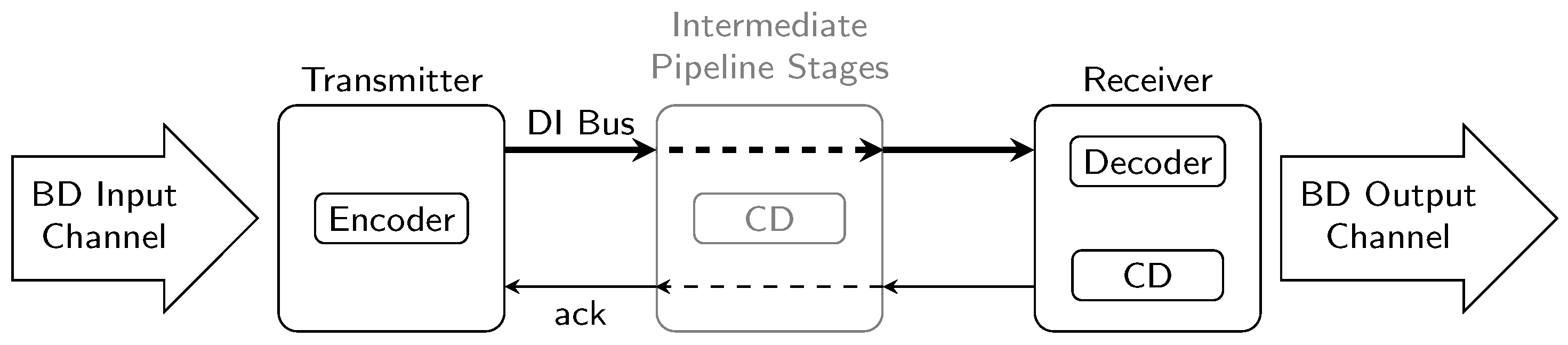
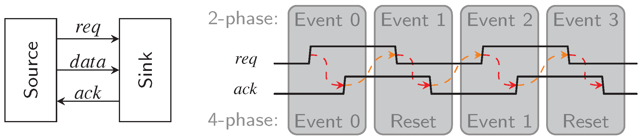
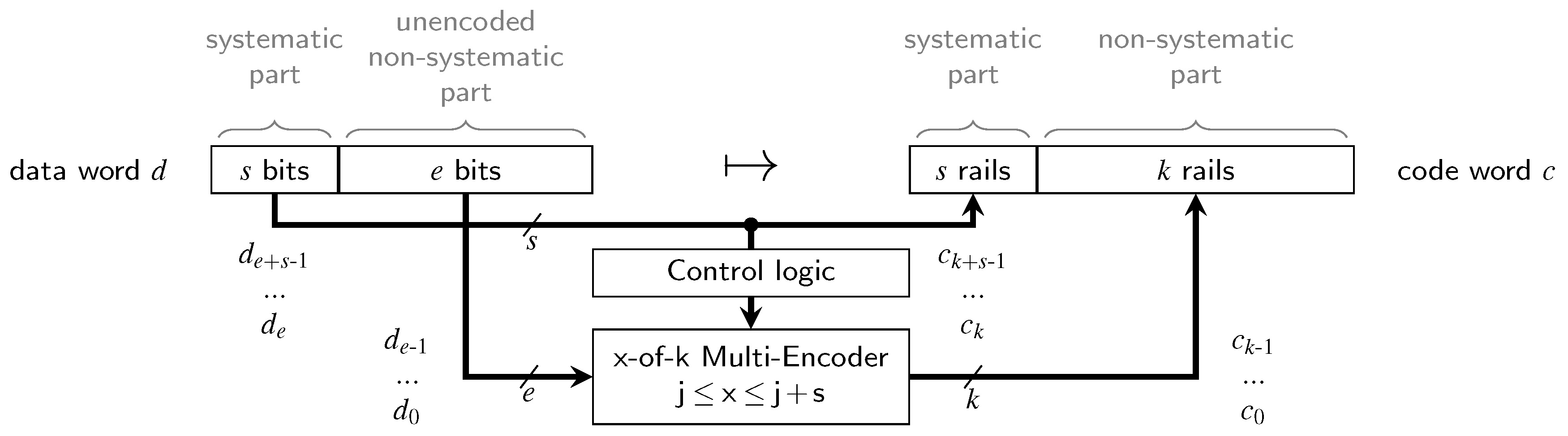
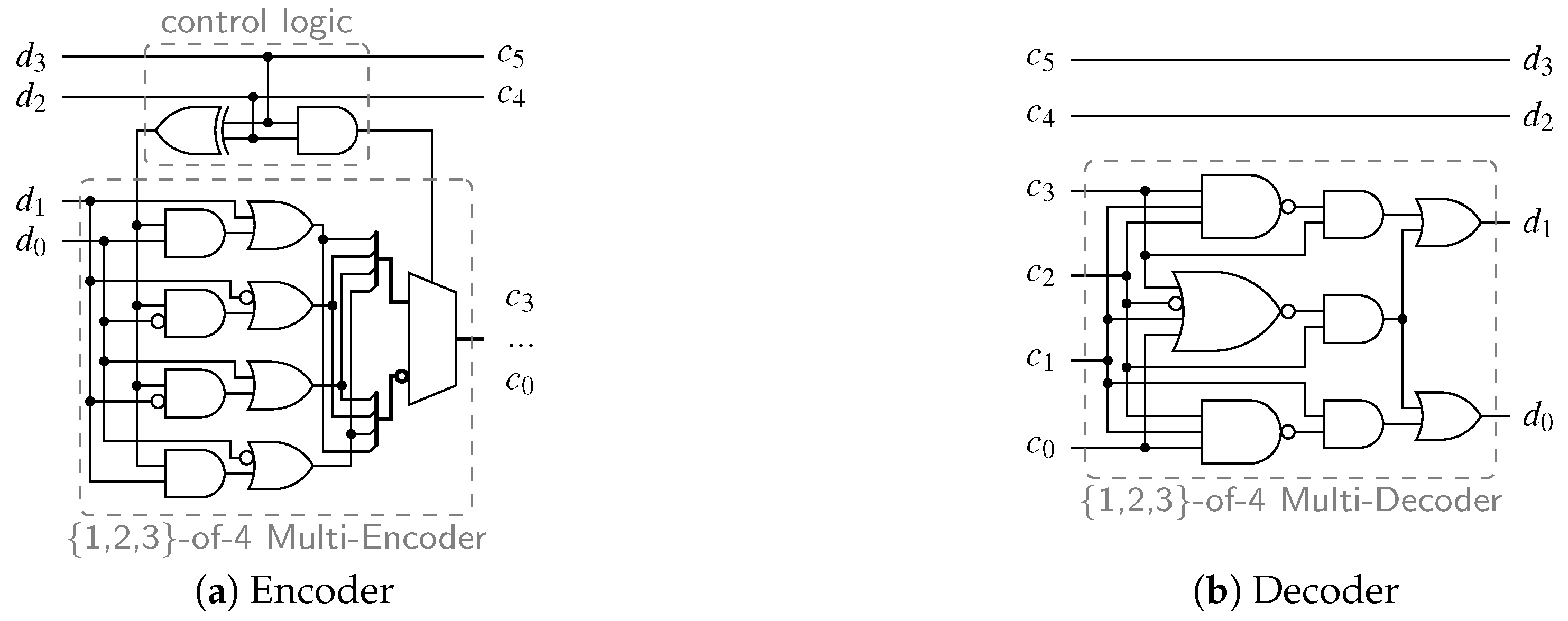
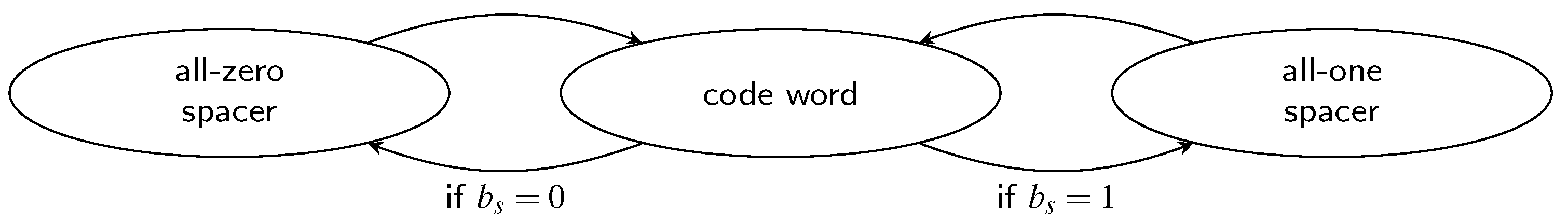
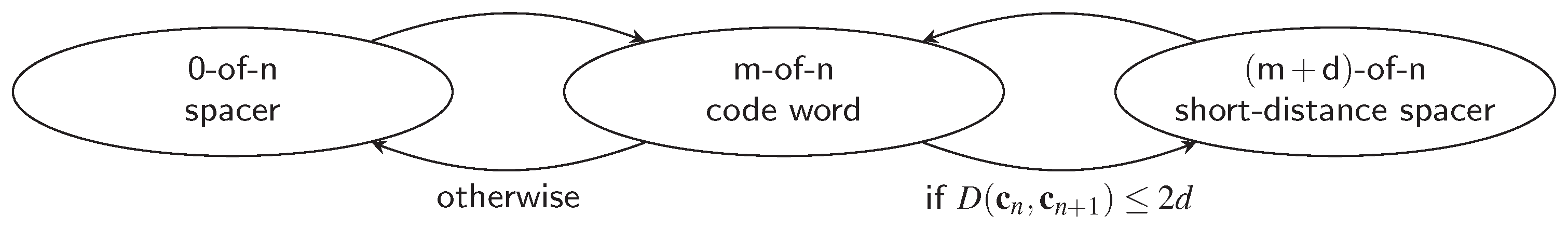
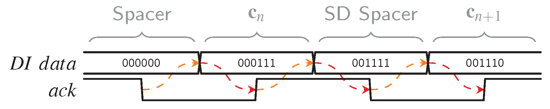
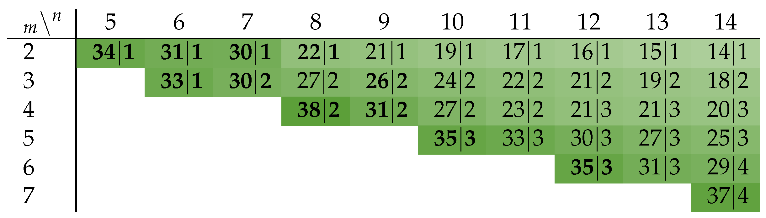
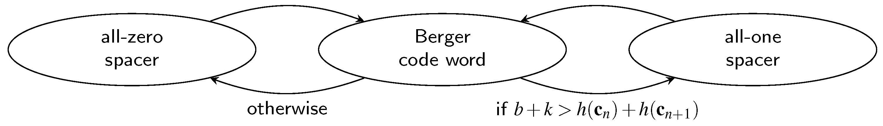
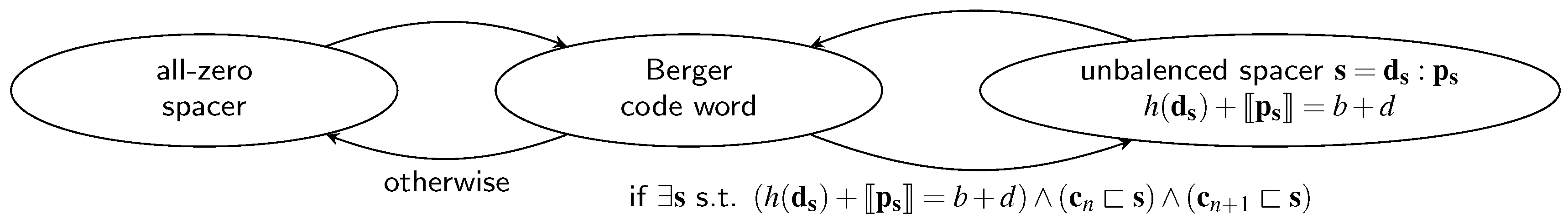
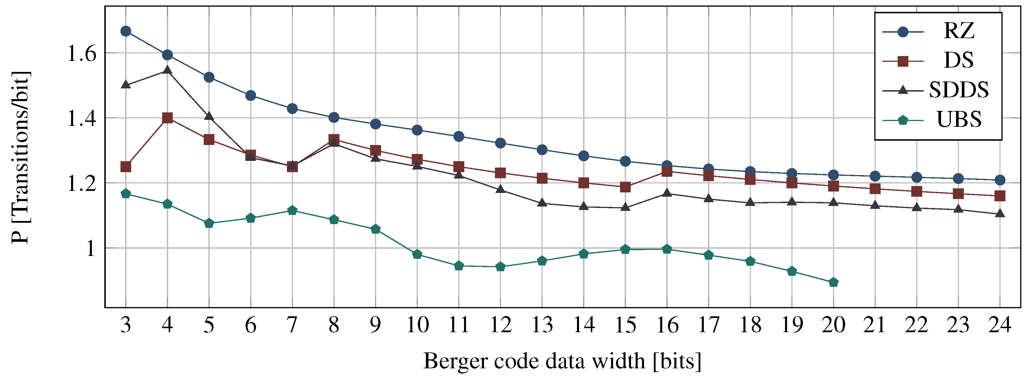
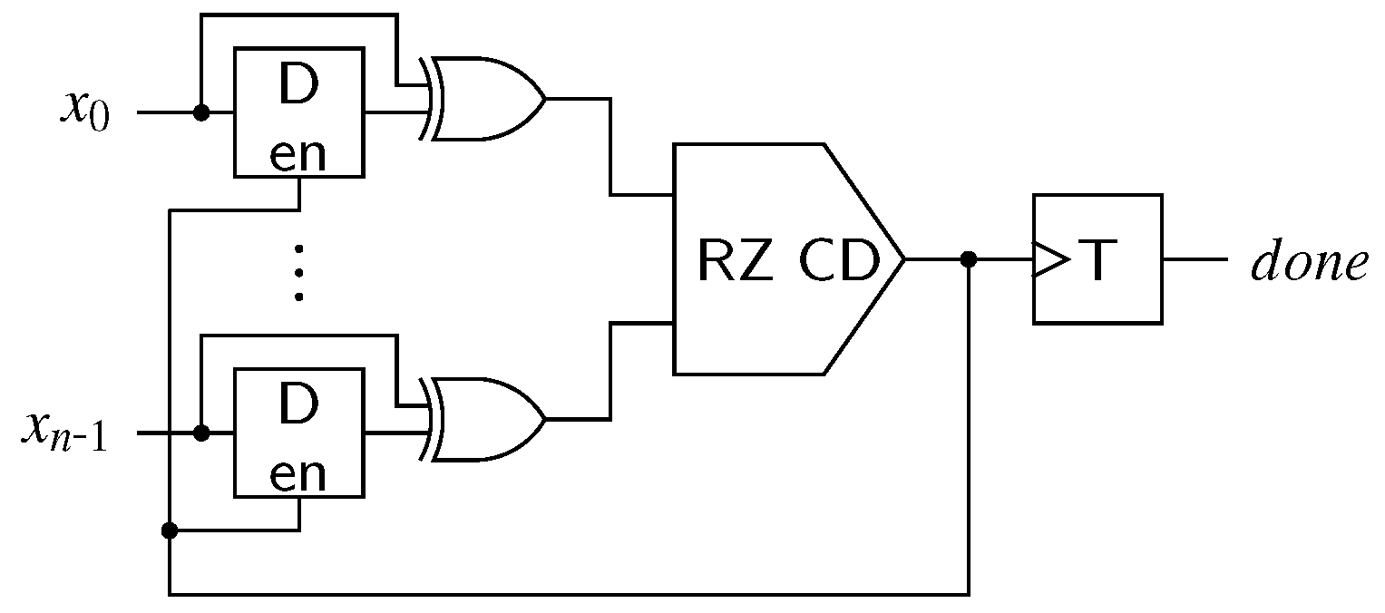
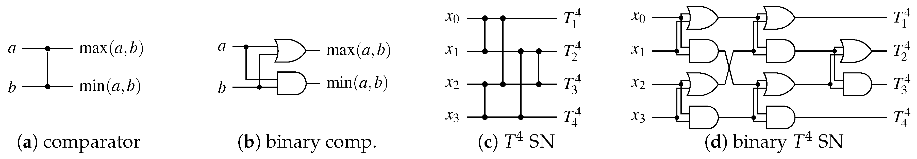
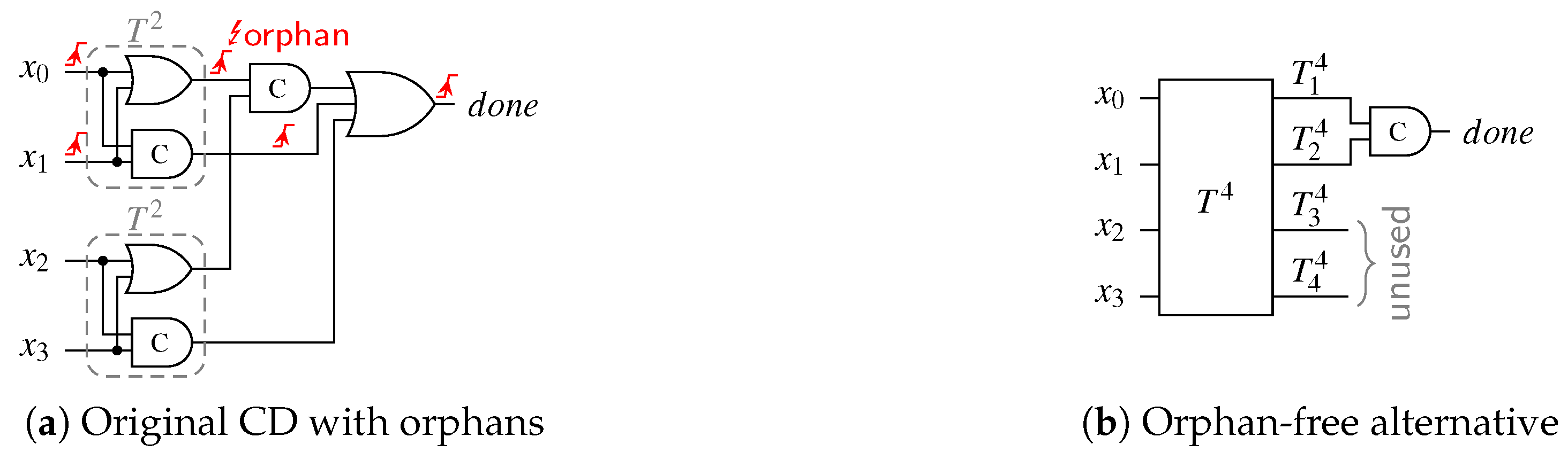
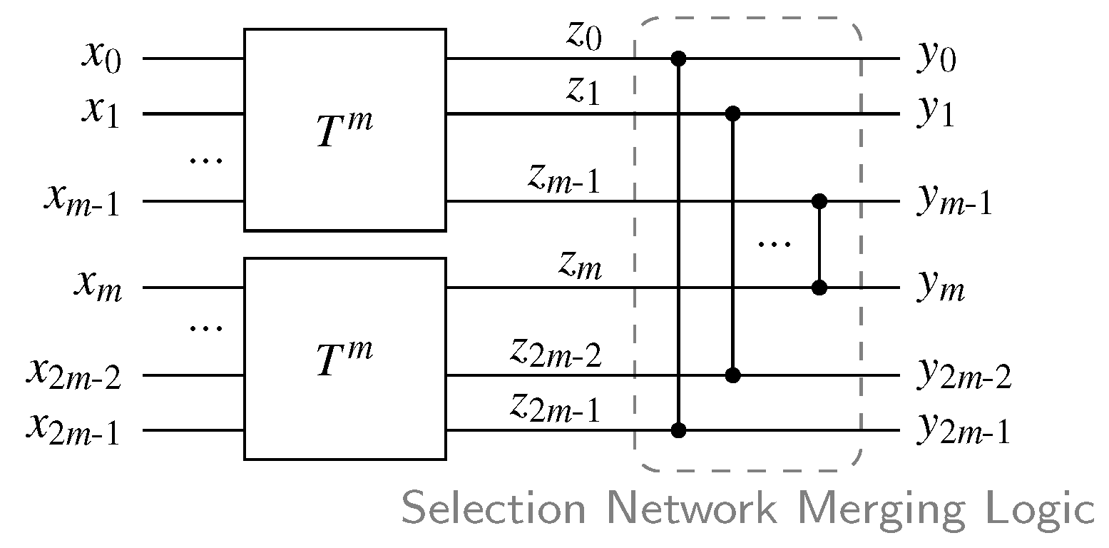
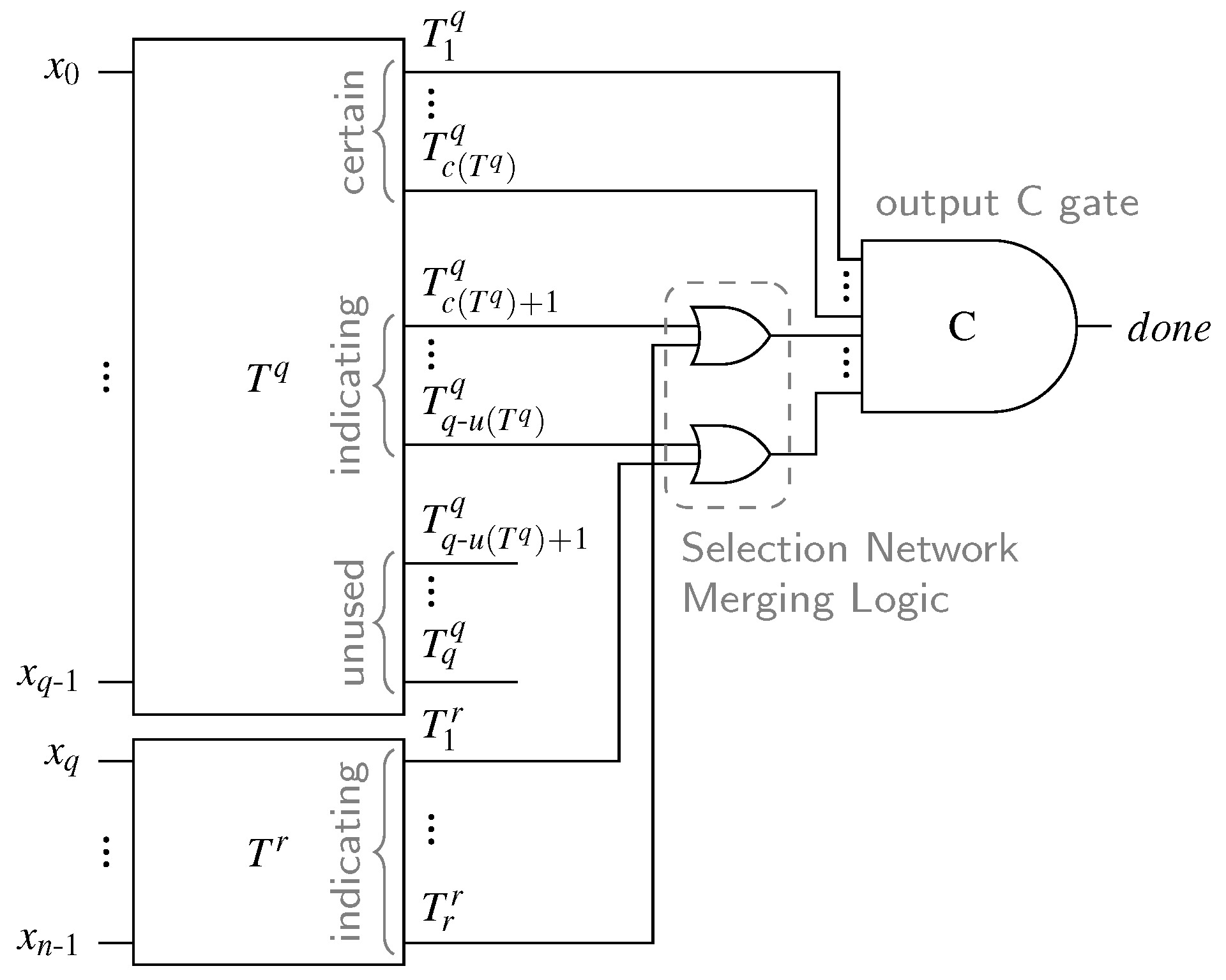
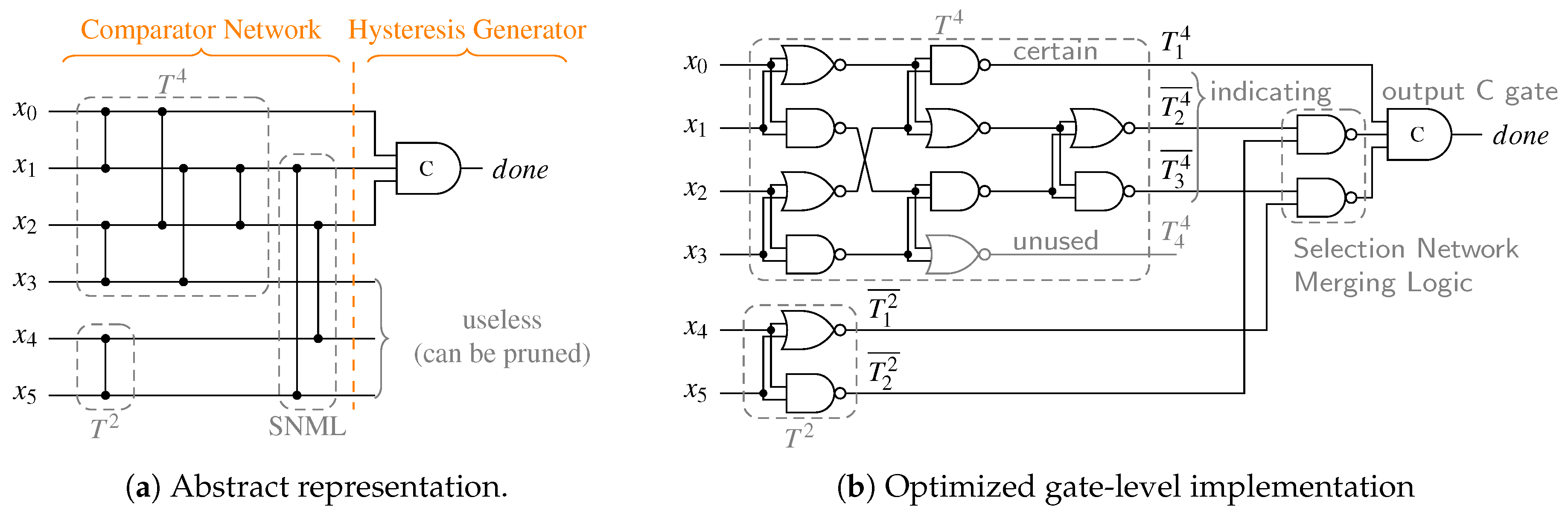
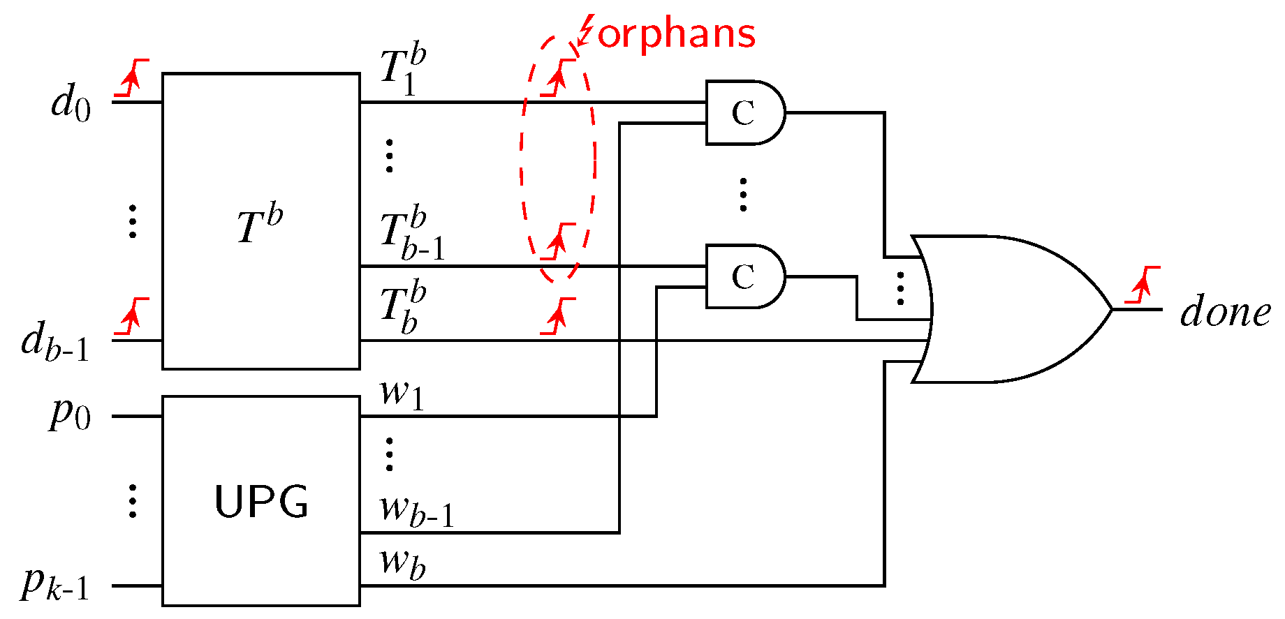
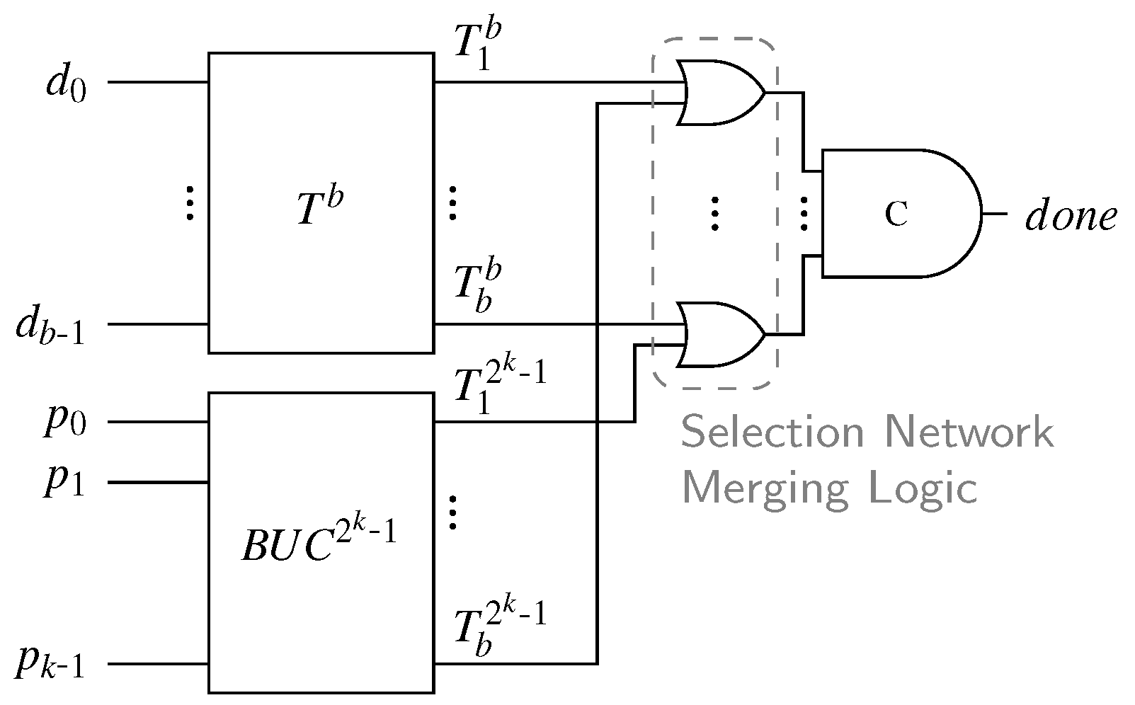
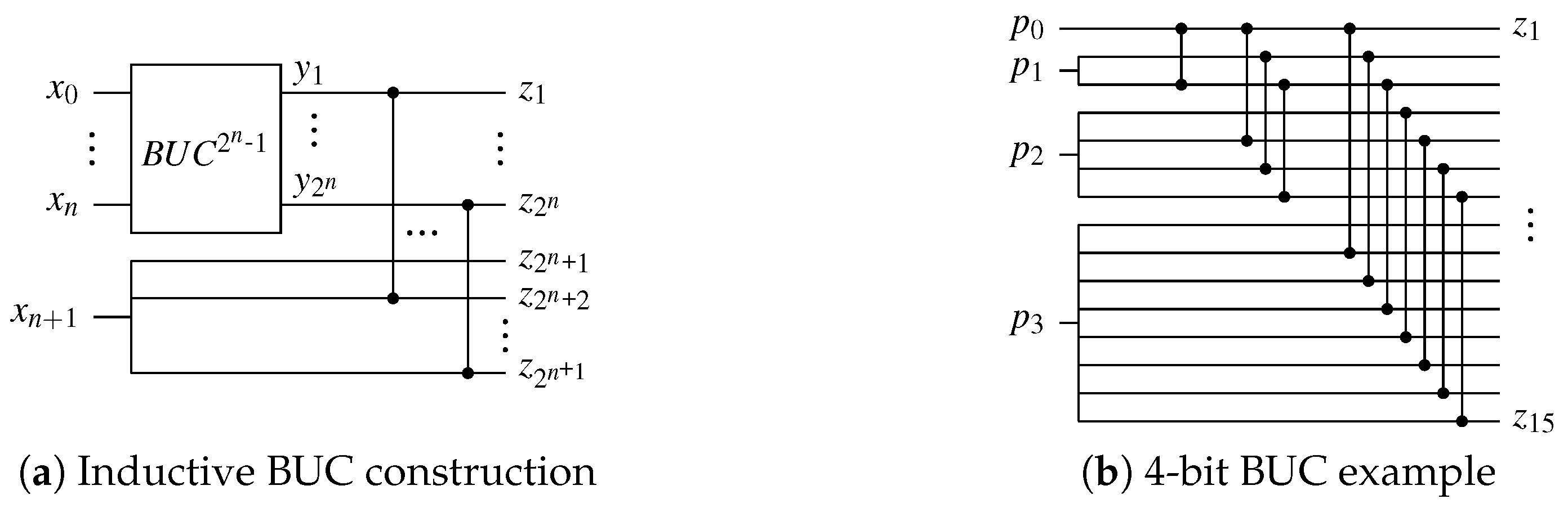
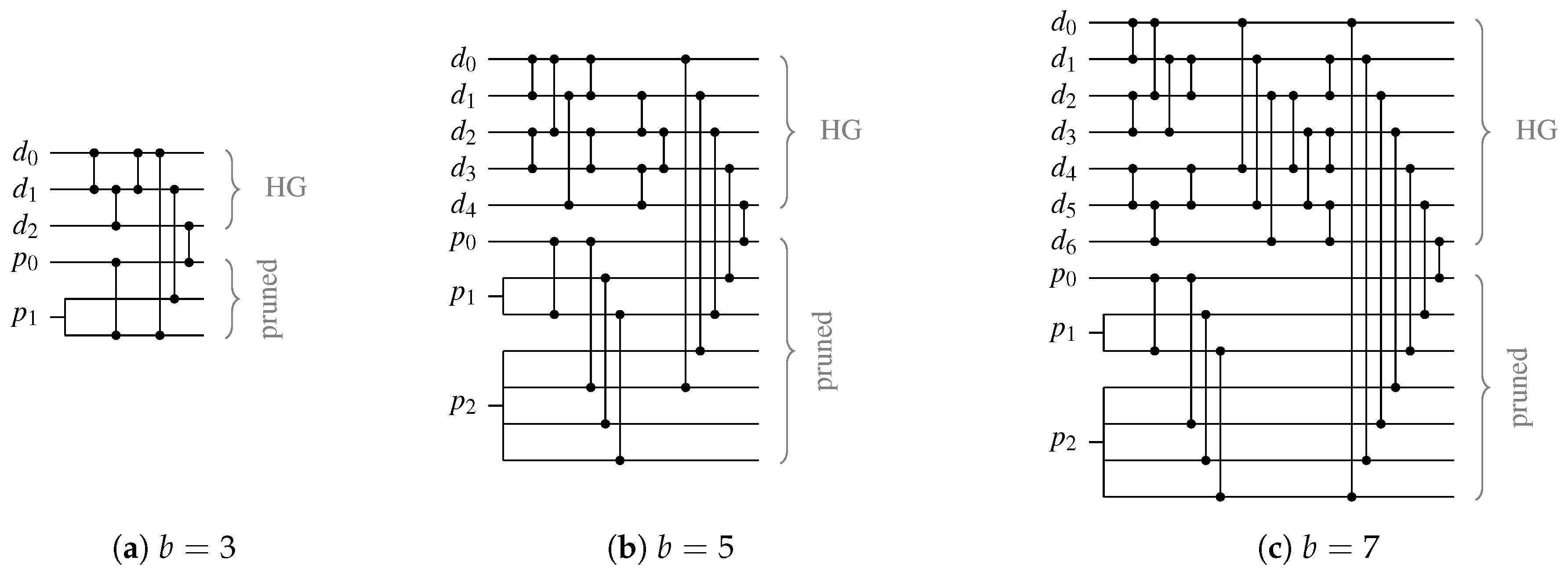
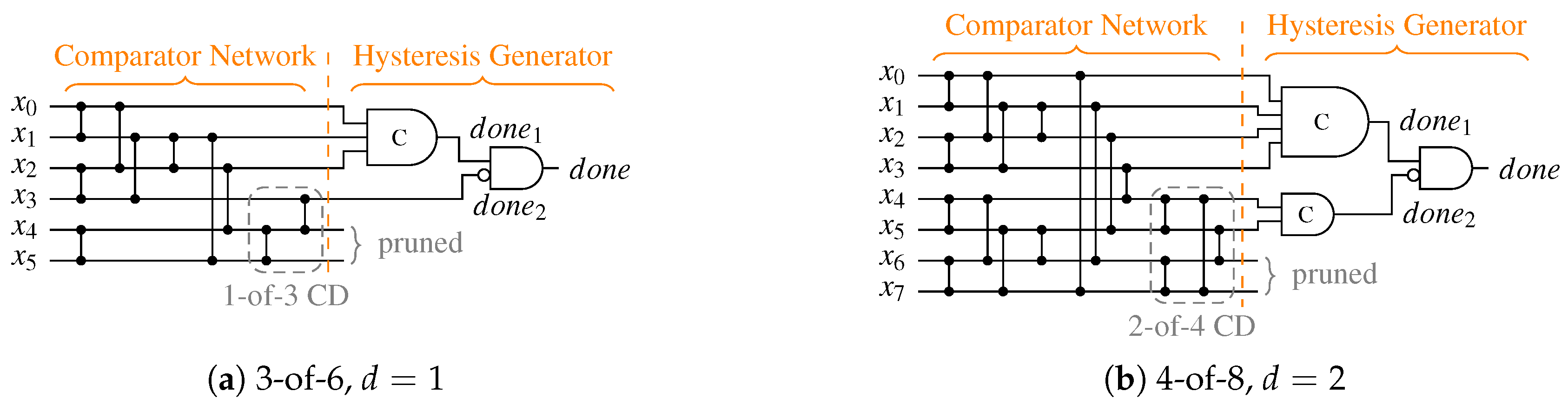
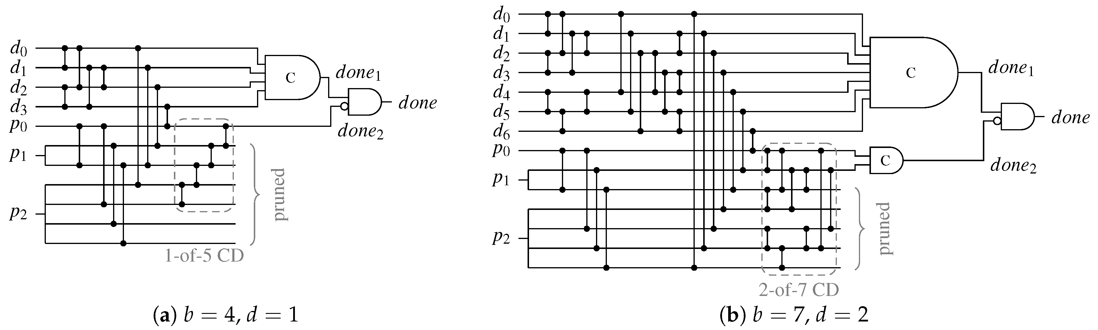
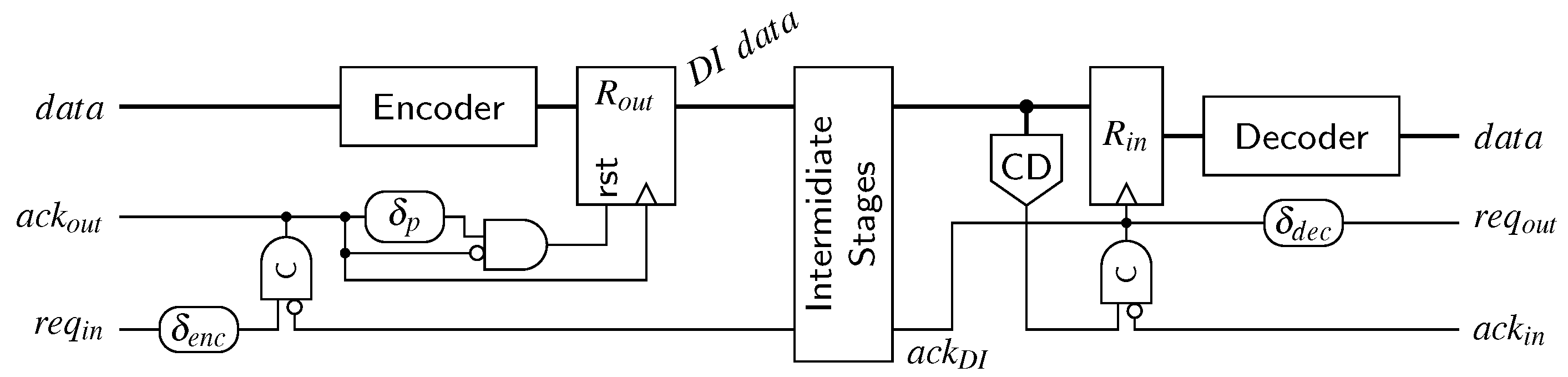
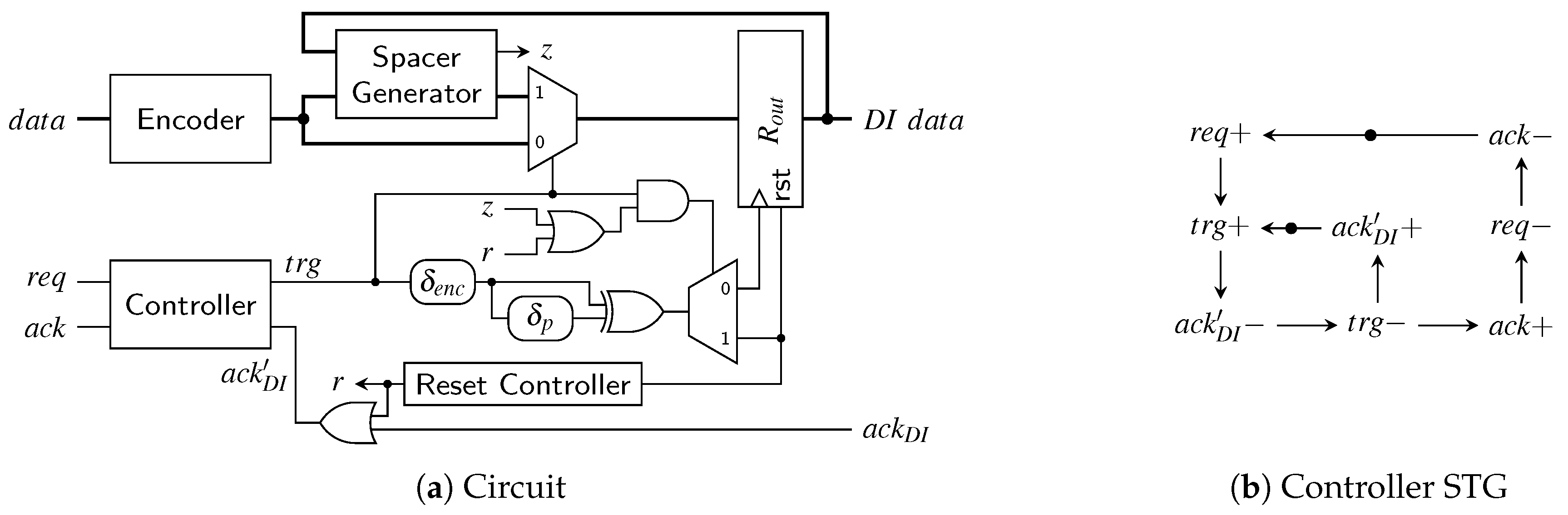
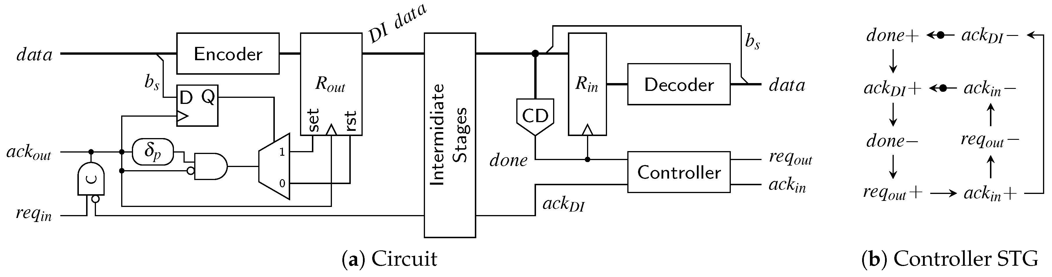
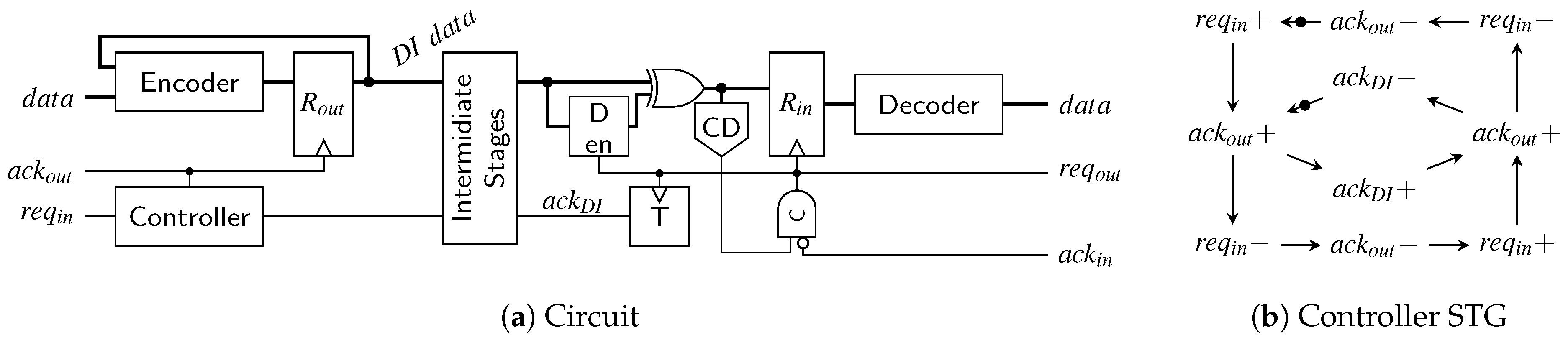
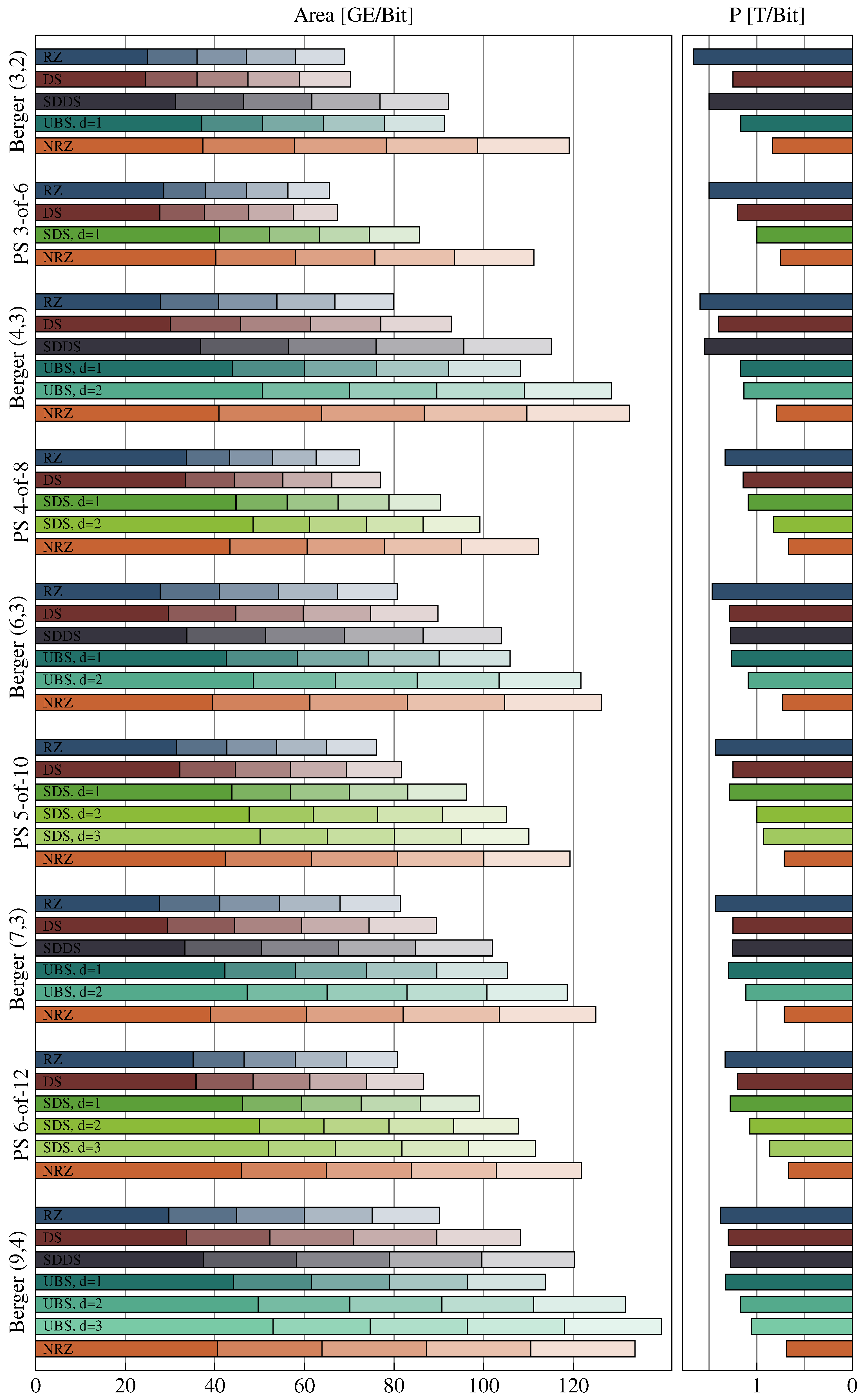
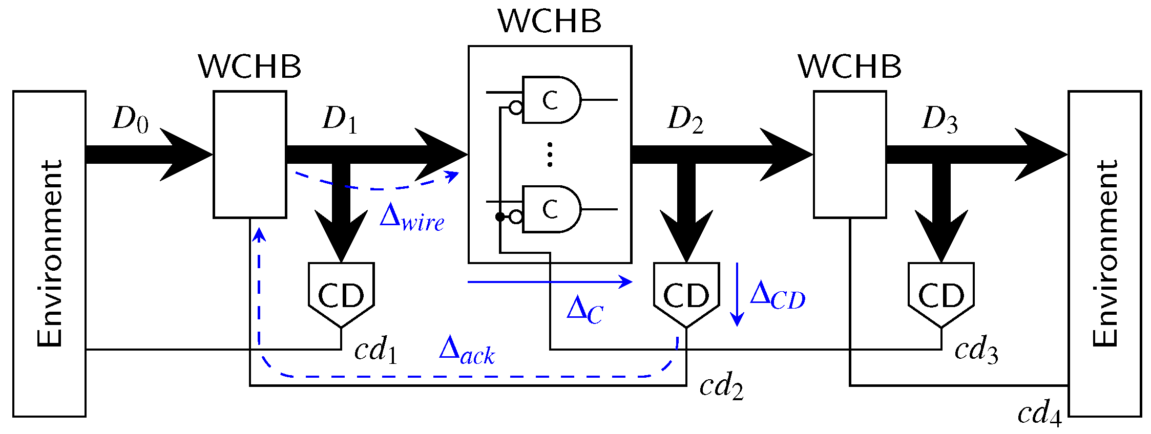
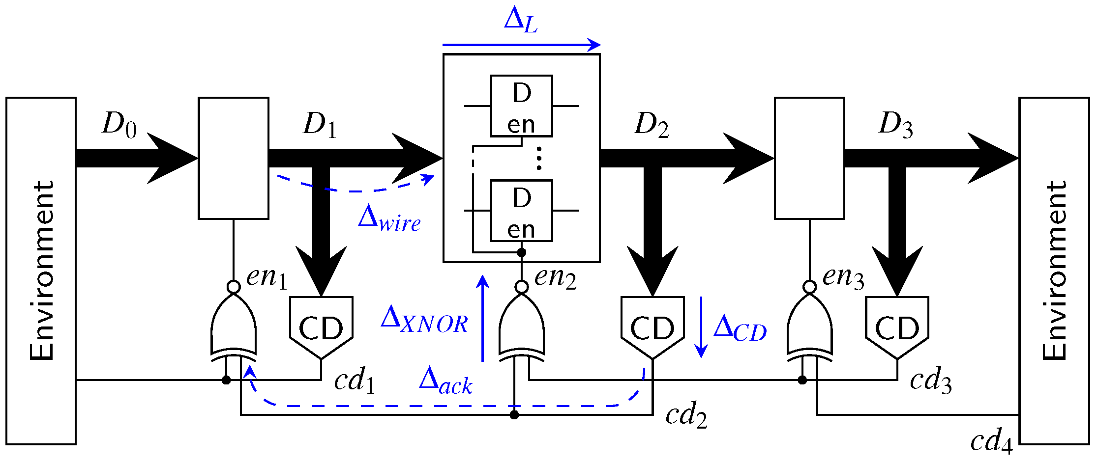
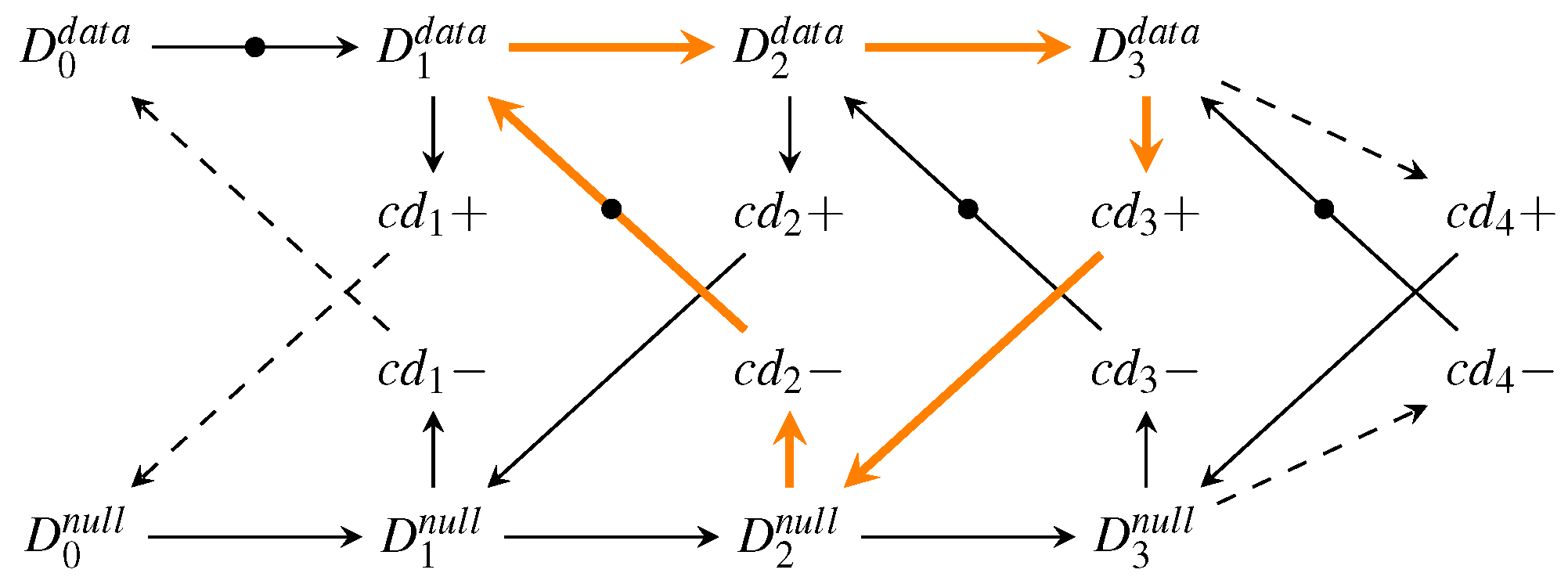
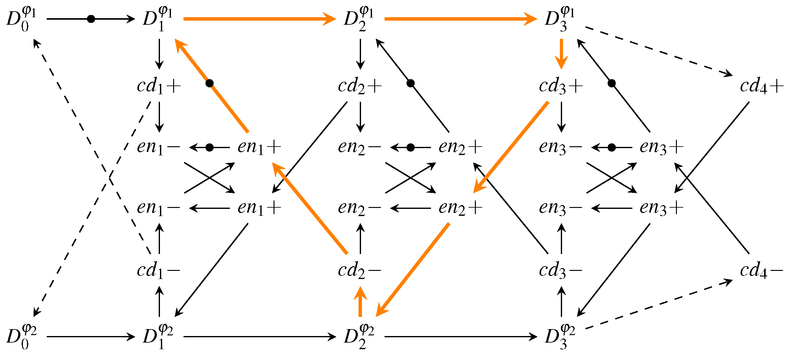
Table 1.
Examples for Partially Systematic Codes.
| Code | # Systematic Bits | # Non-Systematic Bits |
|---|---|---|
| 3-of-6 | 2 | 2 |
| 4-of-8 | 1 | 5 |
| 5-of-10 | 3 | 4 |
| 6-of-12 | 3 | 6 |
Table 2.
{1,2,3}-of-4 multi-encoder for the PS 3-of-6 code .
| Condition | |||
|---|---|---|---|
| 2 | 1-of-4 | - | |
| 1 | 2-of-4 | - | |
| 0 | 3-of-4 | - |
Table 3.
{3,4}-of-7 multi-encoder for PS 4-of-8 code .
| Condition | |||||
|---|---|---|---|---|---|
| 1 | 3-of-7 | 000 | |||
| 0 | 4-of-7 | 111 | |||
| ) | |||||
Table 4.
{2,3,4,5}-of-7 multi-encoder for the PS 5-of-10 code .
| Condition | ||||
|---|---|---|---|---|
| 3 | 2-of-7 | 000 | ||
| 2 | 3-of-7 | 000 | ||
| 1 | 4-of-7 | 111 | ||
| 0 | 5-of-7 | 111 | ||
Table 5.
{3,4,5,6}-of-9 multi-encoder for the PS 6-of-12 code .
| Condition | ||||
|---|---|---|---|---|
| 3 | 3-of-9 | 00 | ||
| 2 | 4-of-9 | - | ||
| 1 | 5-of-9 | - | ||
| 0 | 6-of-9 | 11 | ||
Table 6.
d values used for the power metric evaluation of the UBS protocol.
| b | 3 | 20 | |||||
| d | 1 | 2 | 3 | 5 | 6 | 7 | 10 |
Table 7.
SN implementation costs (minimal depth).
| n | 3 | 4 | 5 | 6 | 7 | 8 | 9 | 10 | 11 | 12 | 13 | 14 | 15 | 16 |
|---|---|---|---|---|---|---|---|---|---|---|---|---|---|---|
| 3 | 5 | 9 | 12 | 16 | 19 | 25 | 31 | 35 | 40 | 47 | 52 | 57 | 61 | |
| 3 | 3 | 5 | 5 | 6 | 6 | 7 | 7 | 8 | 8 | 9 | 9 | 9 | 9 |
Table 8.
Hardware overhead for encoders and decoders.
| Code | # Rails | # Bits | R | Encoder Overhead [GE/bit] | Decoder Overhead [GE/bit] | |||||
|---|---|---|---|---|---|---|---|---|---|---|
| RZ | SDS/UBS (d) | SDDS | NRZ | |||||||
| 1 | 2 | 3 | ||||||||
| PS 3-of-6 | 6 | 4 | 0.67 | 3.67 | 14.67 | – | – | – | 7.33 | 1.67 |
| PS 4-of-8 | 8 | 6 | 0.75 | 6.61 | 16.44 | 18.94 | – | – | 9.28 | 4.89 |
| PS 5-of-10 | 10 | 7 | 0.70 | 5.33 | 16.14 | 18.67 | 20.52 | – | 8.52 | 1.71 |
| PS 6-of-12 | 12 | 9 | 0.75 | 6.63 | 16.33 | 18.78 | 20.48 | – | 10.33 | 4.63 |
| Berger (3,2) | 5 | 3 | 0.60 | 2.22 | 12.33 | – | – | 2.56 | 5.67 | 0.00 |
| Berger (4,3) | 7 | 4 | 0.57 | 2.75 | 16.33 | 19.58 | – | 3.42 | 6.50 | 0.00 |
| Berger (5,3) | 8 | 5 | 0.62 | 2.87 | 15.40 | 17.93 | – | 3.33 | 6.47 | 0.00 |
| Berger (6,3) | 9 | 6 | 0.67 | 3.39 | 16.06 | 19.67 | – | 3.56 | 7.11 | 0.00 |
| Berger (7,3) | 10 | 7 | 0.70 | 3.33 | 16.05 | 18.90 | – | 3.86 | 7.00 | 0.00 |
| Berger (8,4) | 12 | 8 | 0.67 | 4.04 | 17.04 | 19.62 | 20.88 | 5.25 | 7.25 | 0.00 |
| Berger (9,4) | 13 | 9 | 0.69 | 3.67 | 16.30 | 18.63 | 20.85 | 4.41 | 6.85 | 0.00 |
Table 9.
Hardware overhead [GE/bit] for completion detectors (combinational/sequential costs).
| Code | RZ | SDS/UBS (d) | SDDS | DS | NRZ | ||
|---|---|---|---|---|---|---|---|
| 1 | 2 | 3 | |||||
| PS 3-of-6 | 3.25/1.50 | 4.67/1.50 | – | – | – | 3.53/2.40 | 6.25/6.50 |
| PS 4-of-8 | 4.11/1.56 | 5.39/1.56 | 6.17/2.06 | – | – | 4.43/2.67 | 6.78/6.00 |
| PS 5-of-10 | 5.43/1.43 | 6.90/1.43 | 7.76/1.86 | 7.95/2.29 | – | 5.71/2.50 | 8.29/6.19 |
| PS 6-of-12 | 6.07/1.33 | 7.44/1.33 | 8.37/1.67 | 8.44/2.00 | – | 6.30/2.40 | 8.74/5.78 |
| Berger (3,2) | 4.00/2.00 | 6.00/2.00 | – | – | 5.67/4.00 | 4.25/3.00 | 7.33/7.56 |
| Berger (4,3) | 5.42/2.33 | 7.92/2.33 | 10.58/3.08 | – | 8.25/5.50 | 6.60/4.40 | 8.92/8.17 |
| Berger (5,3) | 6.53/2.00 | 8.53/2.00 | 11.53/2.60 | – | 8.73/4.53 | 7.28/3.78 | 9.73/7.33 |
| Berger (6,3) | 6.72/2.00 | 8.83/2.00 | 10.78/2.50 | – | 8.44/4.11 | 7.24/3.52 | 9.72/7.00 |
| Berger (7,3) | 7.33/1.81 | 9.19/1.81 | 10.86/2.24 | – | 8.76/3.62 | 7.67/3.17 | 10.19/6.57 |
| Berger (8,4) | 8.38/1.67 | 10.42/1.67 | 12.96/2.04 | 14.42/2.42 | 11.08/4.71 | 9.85/4.19 | 11.38/6.67 |
| Berger (9,4) | 9.22/1.56 | 11.04/1.56 | 13.81/1.89 | 14.63/2.22 | 11.63/4.26 | 10.47/3.83 | 12.11/6.37 |
Table 10.
Parameters for the delay estimations of m-of-n CDs for the RZ and SDS protocols.
| Code | ||||
|---|---|---|---|---|
| 1 | 2 | 3 | ||
| PS 3-of-6 | 4 | 5/0.50 | – | – |
| PS 4-of-8 | 4 | 6/0.24 | 6/0.76 | – |
| PS 5-of-10 | 6 | 8/0.12 | 9/0.5 | 9/0.88 |
| PS 6-of-12 | 6 | 8/0.05 | 10/0.29 | 10/0.71 |
Table 11.
Parameters for the delay estimations of Berger CDs for the RZ and UBS protocols.
| Code | ||||
|---|---|---|---|---|
| 1 | 2 | 3 | ||
| Berger (3,2) | 4 | 5/0.50 | – | – |
| Berger (4,3) | 4 | 6/0.38 | 8/0.65 | – |
| Berger (5,3) | 6 | 8/0.27 | 10/0.53 | – |
| Berger (6,3) | 6 | 8/0.18 | 10/0.44 | – |
| Berger (7,3) | 7 | 9/0.12 | 11/0.36 | – |
| Berger (8,4) | 7 | 9/0.07 | 12/0.29 | 13/0.48 |
| Berger (9,4) | 8 | 10/0.05 | 13/0.22 | 14/0.45 |
© 2019 by the authors. Licensee MDPI, Basel, Switzerland. This article is an open access article distributed under the terms and conditions of the Creative Commons Attribution (CC BY) license (http://creativecommons.org/licenses/by/4.0/).
Share and Cite
MDPI and ACS Style
Huemer, F.; Steininger, A. Novel Approaches for Efficient Delay-Insensitive Communication. J. Low Power Electron. Appl. 2019, 9, 16. https://doi.org/10.3390/jlpea9020016
AMA Style
Huemer F, Steininger A. Novel Approaches for Efficient Delay-Insensitive Communication. Journal of Low Power Electronics and Applications. 2019; 9(2):16. https://doi.org/10.3390/jlpea9020016
Chicago/Turabian StyleHuemer, Florian, and Andreas Steininger. 2019. "Novel Approaches for Efficient Delay-Insensitive Communication" Journal of Low Power Electronics and Applications 9, no. 2: 16. https://doi.org/10.3390/jlpea9020016
Note that from the first issue of 2016, this journal uses article numbers instead of page numbers. See further details here.