Article

An Improved Proposed Single Phase Transformerless Inverter with Leakage Current Elimination and Reactive Power Capability for PV Systems Application †

Department of Electrical and Computer Engineering, University of Denver, 2155 East Wesley Avenue, Denver, CO 80208, USA
*
Author to whom correspondence should be addressed.
This paper is an extended version of our paper published in the 2017 IEEE International Conference on Electro Information Technology (EIT), Lincoln, NE, USA, 14–17 May 2017.
J. Low Power Electron. Appl. 2018, 8(3), 29; https://doi.org/10.3390/jlpea8030029
Submission received: 16 July 2018 / Revised: 22 August 2018 / Accepted: 25 August 2018 / Published: 6 September 2018

Abstract

:
Single-phase transformerless inverters are broadly studied in literature for residential-scale PV applications due to their great advantages in reducing system weight, cost and elevating system efficiency. The design of transformerless inverters is based on the galvanic isolation method to eliminate the generation of leakage current. Unfortunately, the use of the galvanic isolation method alone cannot achieve constant common mode voltage (CMV). Therefore, a complete elimination of leakage current cannot be achieved. In addition, modulation techniques of single-phase transformerless inverters are designed for the application of the unity power factor. Indeed, next-generation PV systems are required to support reactive power to enable connectivity to the utility grid. In this paper, a proposed single-phase transformerless inverter is modified with the clamping method to achieve constant CMV during all inverter operating modes. Furthermore, the modulation technique is modified by creating a new current path in the negative power region. As a result, a bidirectional current path is created in the negative power region to achieve reactive power generation. The simulation results show that the CMV is completely clamped at half the DC link voltage and the leakage current is almost completely eliminated. Furthermore, a reactive power generation is achieved with the modified modulation techniques. Additionally, the total harmonic distortion (THD) of the grid current with the conventional and a modified modulation technique is analyzed. The efficiency of the system is enhanced by using wide-bandgap (WBG) switching devices such as SiC MOSFET. It is observed that the efficiency of the system decreased with reactive power generation due to the bidirectional current path, which leads to increasing conduction losses.

1. Introduction

Several transformerless inverter topologies have been presented and published [1,2,3,4,5,6,7]. One of the drawbacks of PV transformerless inverters is the generating of leakage current due to the absence of a transformer. High generation of leakage current increases system losses, total harmonic distortion (THD), electromagnetic interference (EMI) and can cause personal safety issues [8,9,10,11]. The literature cites various modulation techniques that have been used to eliminate or minimize leakage current.
Many transformerless inverter topologies with unipolar modulation technique have been introduced to increase system efficiency and reduce the leakage current by disconnecting the AC and DC sides during the freewheeling modes; this is known as galvanic isolation. Many topologies have been derived and developed based on this method, including a highly efficient and reliable inverter concept (HERIC), the H5 inverter and the H6 topology [12,13]. However, complete elimination of leakage current cannot be achieved with the galvanic isolation method alone because common mode voltage (CMV) during freewheeling periods cannot be identified by the switching state, which means that it is not constant. Therefore, modulation strategies and converter structures must be modified so that CMV becomes constant during all inverter operating modes.
Most of the modulation techniques are designed for the application of a unity power factor. Indeed, next-generation PV inverters are required to support reactive power to allow for the high penetration of PV inverters to be connected to the utility grid [14,15,16,17,18,19]. Several international standards have been reviewed to achieve reactive power support. As reported by VDE-AR-N4105, PV grid connected inverters must have the ability to generate reactive power.
Considering all this, a traditional bipolar modulation technique is proposed as a possible candidate to be used in next-generation PV inverters, because it has the ability to generate reactive power and eliminate leakage current. Nevertheless, using bipolar modulation techniques to generate reactive power will increase switching losses and degrade system efficiency as it is a two-level modulation.
The Si MOSFET-based transformerless inverter is highly efficient in generating reactive power, but the inverter design must be optimized to address the fact that the Si MOSFET’s body diode has poor reverse recovery performance, which may lead to device failure [20,21]. These inverters are based on the idea of avoiding the conduction of an anti-parallel diode, which will result in a more complicated and complex inverter that in turn increases costs. On the other hand, the SiC MOSFET’s body diode has superior reverse recovery performance because it has a shorter minority carrier lifetime [22,23,24,25,26,27,28,29,30]. Therefore, reactive power generation with SiC MOSFET can be achieved without any alteration to the converter structure or adding any additional freewheeling diodes (FWD).
In this paper, WBG power devices such as SiC MOSFET are used to achieve reactive power generation without altering or modifying the structure of the circuit. Furthermore, the total losses (switching and conduction) are significantly reduced with SiC MOSFET due to its superior characteristics. additionally, high efficiency and low THD is achieved when operating the system at high switching frequency of 100 kHz with SiC MOSFET.

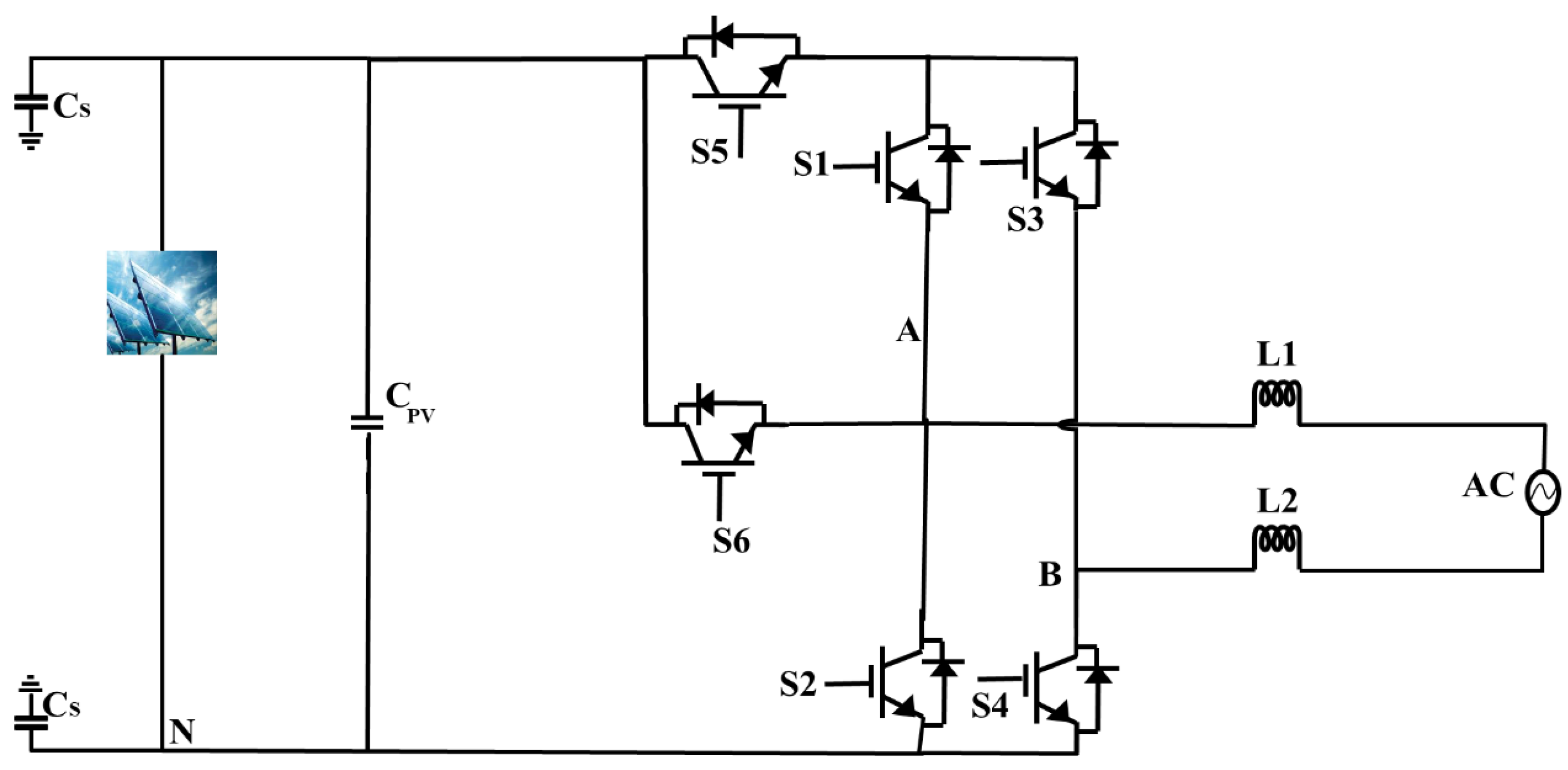
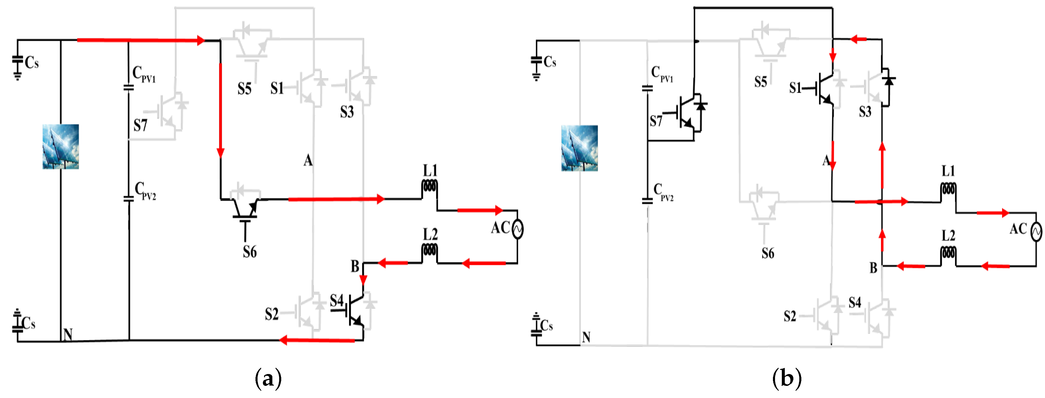
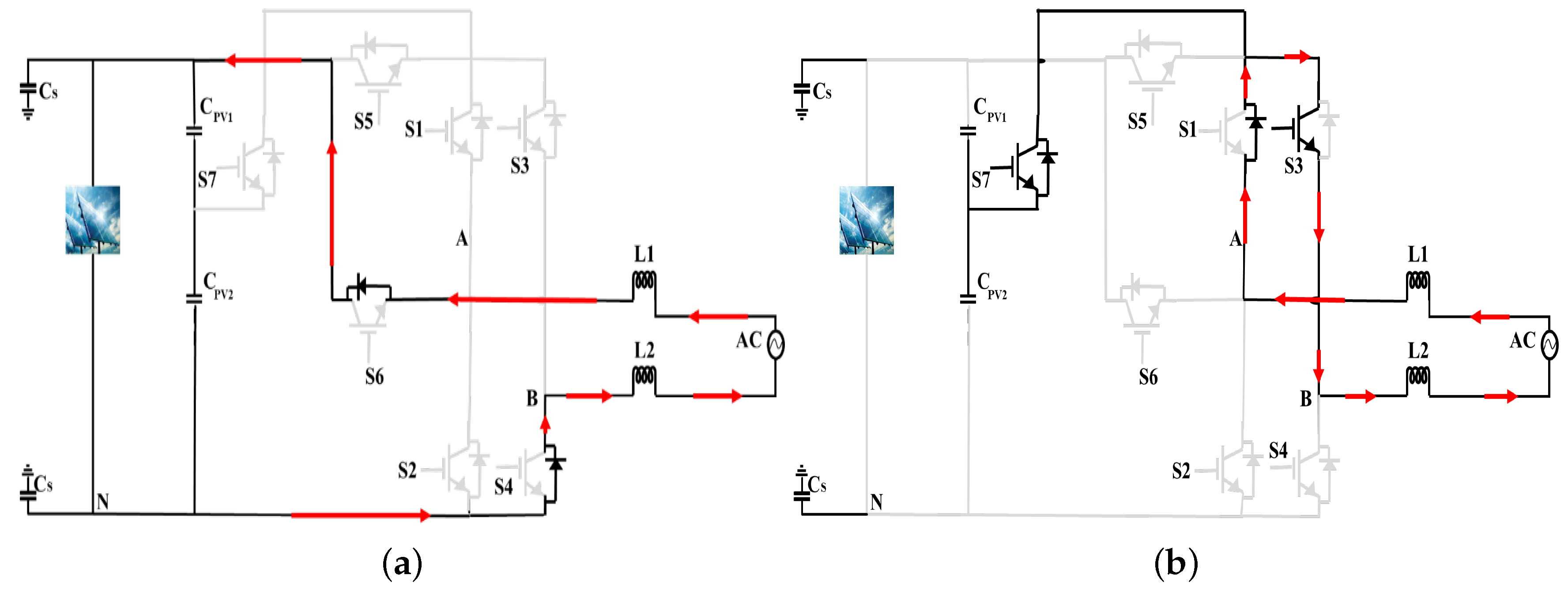
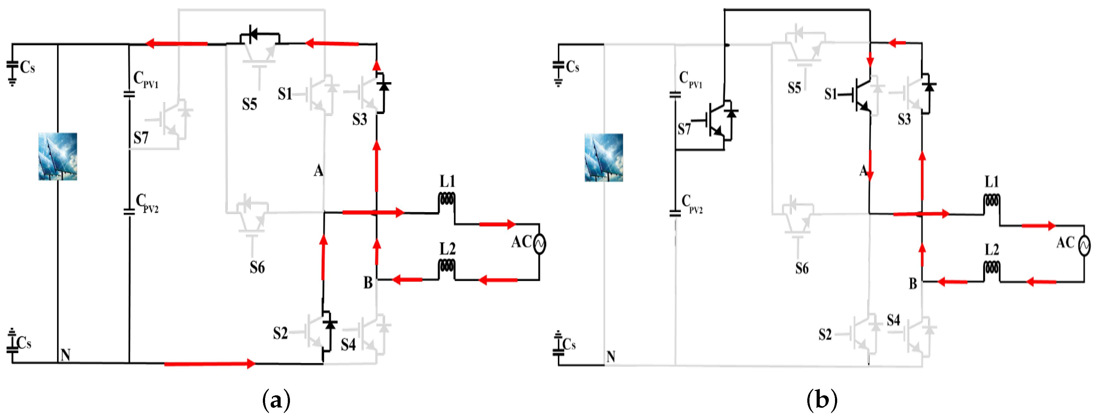
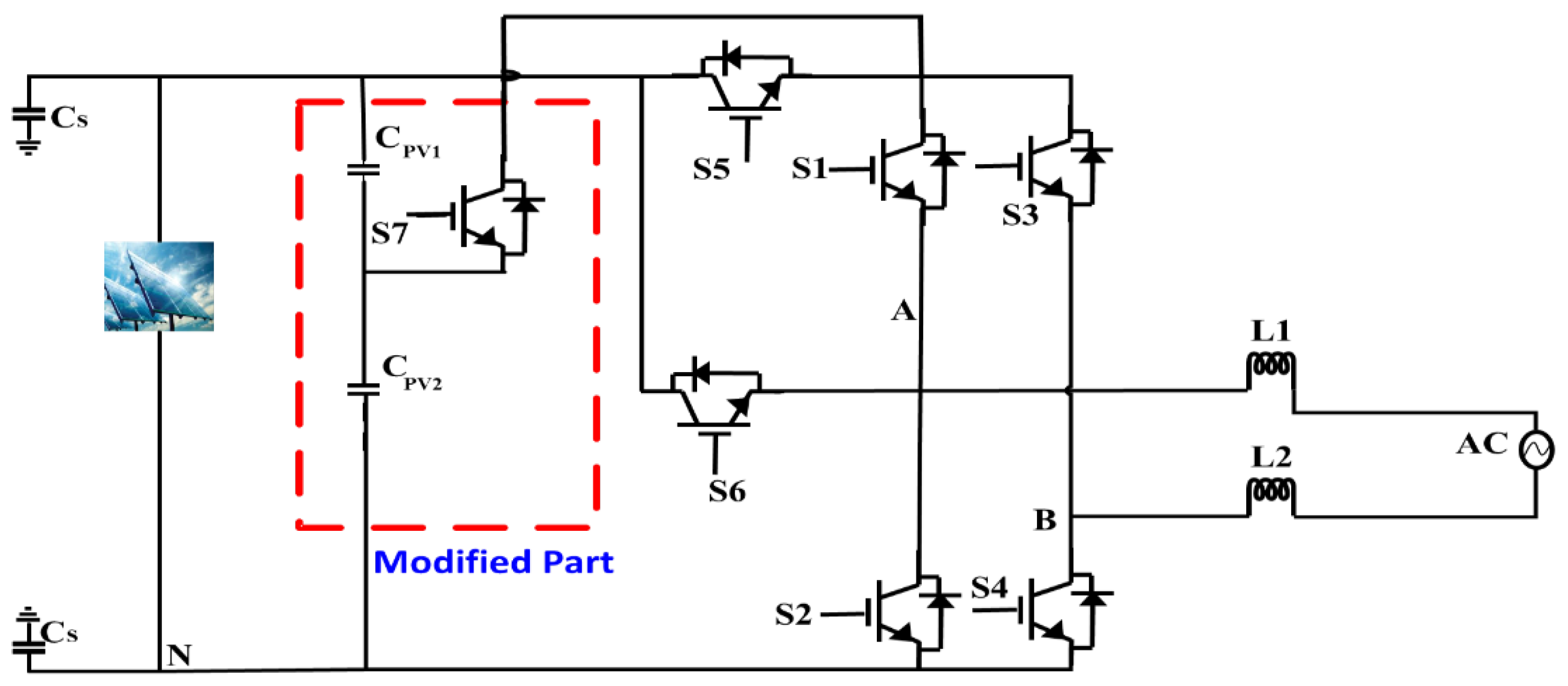
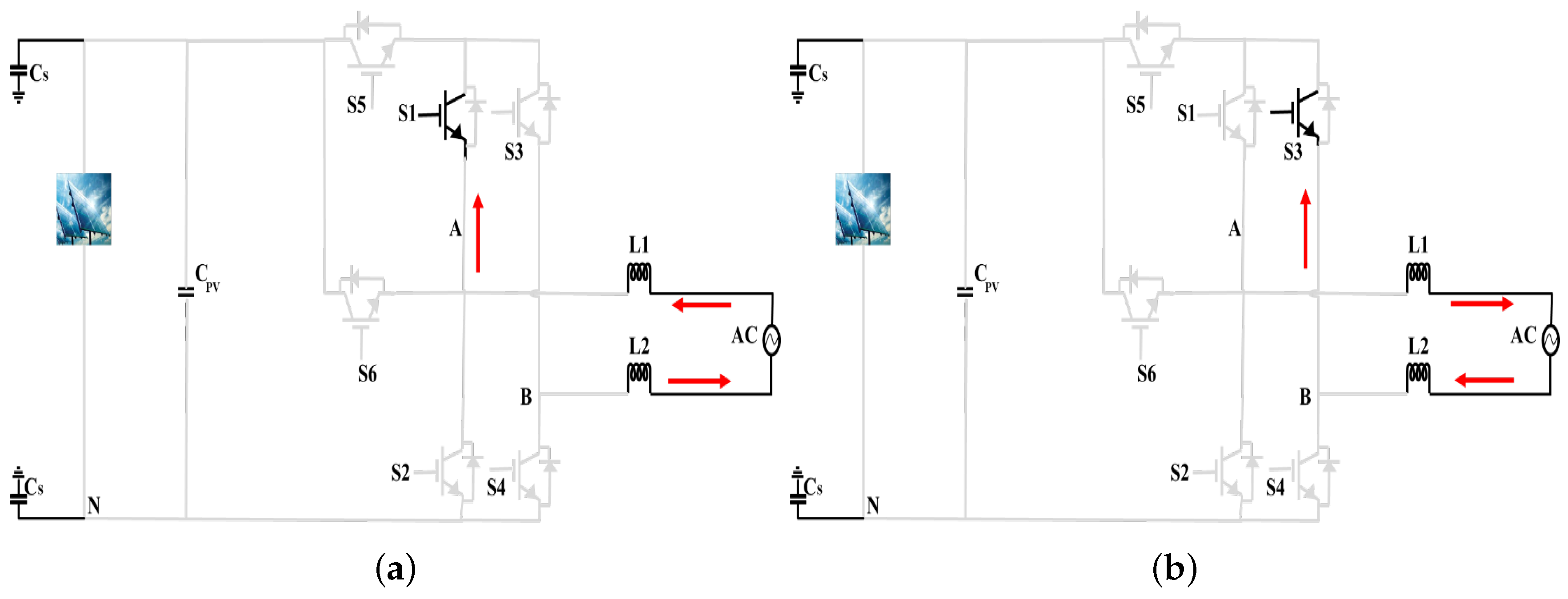
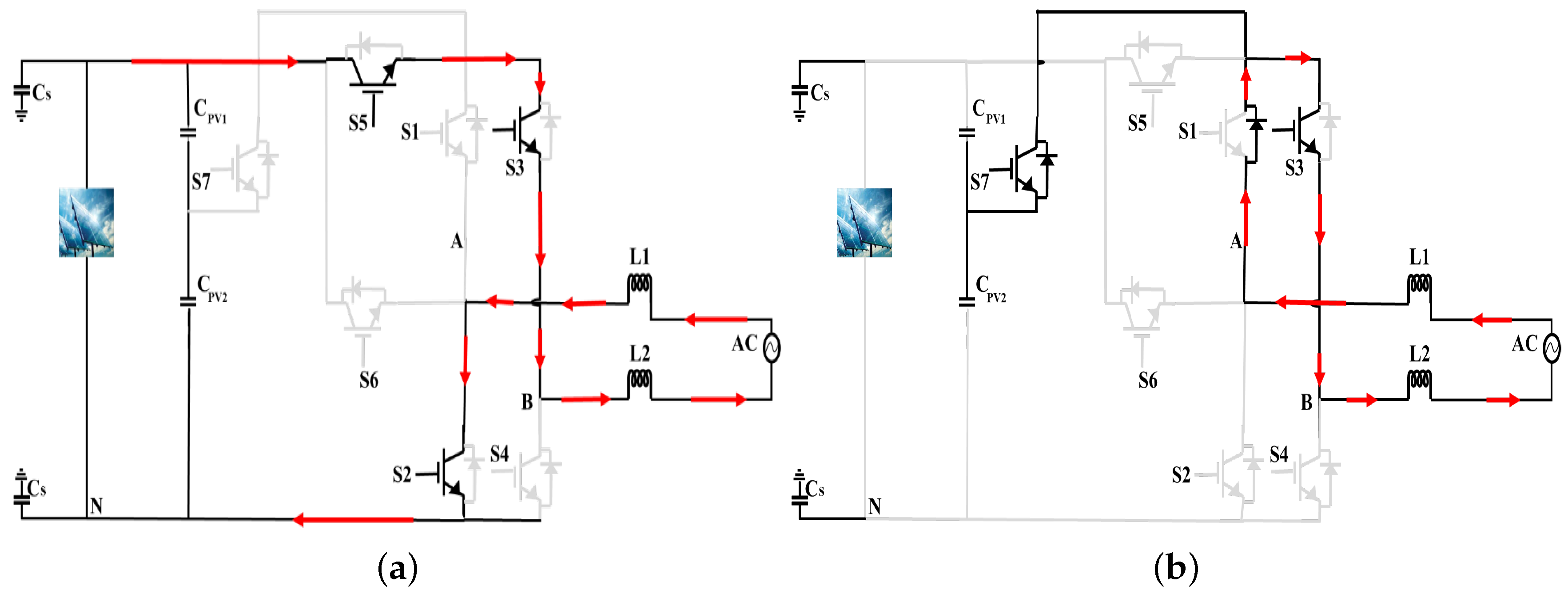
2. Proposed Topology with Leakage Current Elimination and Reactive Power Generation

The proposed H6 topology is derived from the conventional H6 topology where the sixth switch is repositioned and connected to the A terminal [31,32]. The proposed topology and its switching pattern are presented in Figure 1 and Figure 2. The proposed topology has low conduction loss compared to traditional topologies, such as H5 and H6, because the number of conducting switches is reduced from six switches to five switches.
On the other hand, only using galvanic isolation will not maintain the desired constant CMV during the freewheeling period. Since the inverter output terminals A and B are floating during the freewheeling periods with respect to the DC side, this means that CMV cannot be determined from the switching states. Accordingly, the generation of leakage current cannot be fully controlled with the galvanic isolation method. Therefore, the proposed topology is improved by incorporating the clamped method technique to eliminate the leakage current and achieve constant CMV during the freewheeling period, as shown in Figure 3. The DC link capacitor is divided into two series capacitors to achieve the voltage divider. In the clamping method, an extra active switch is added to the proposed topology. This switch is known as a clamping switch and is placed between the midpoint of the freewheeling switches and the midpoint of the DC link capacitors.
The generation of reactive power cannot be accomplished in single-phase transformerless inverter topologies because the existing modulation techniques are not adopted for a freewheeling path in the negative power region. To use unipolar PWM in the negative power region, the line to line voltage (VAB) must have three values, +VDC, −VDC and zero. It is observed that zero voltage states cannot be achieved in the negative power regions because there is no current path established, as illustrated in Figure 4. The modulation method is modified to achieve leakage current elimination and reactive power generation, as shown in Figure 5.

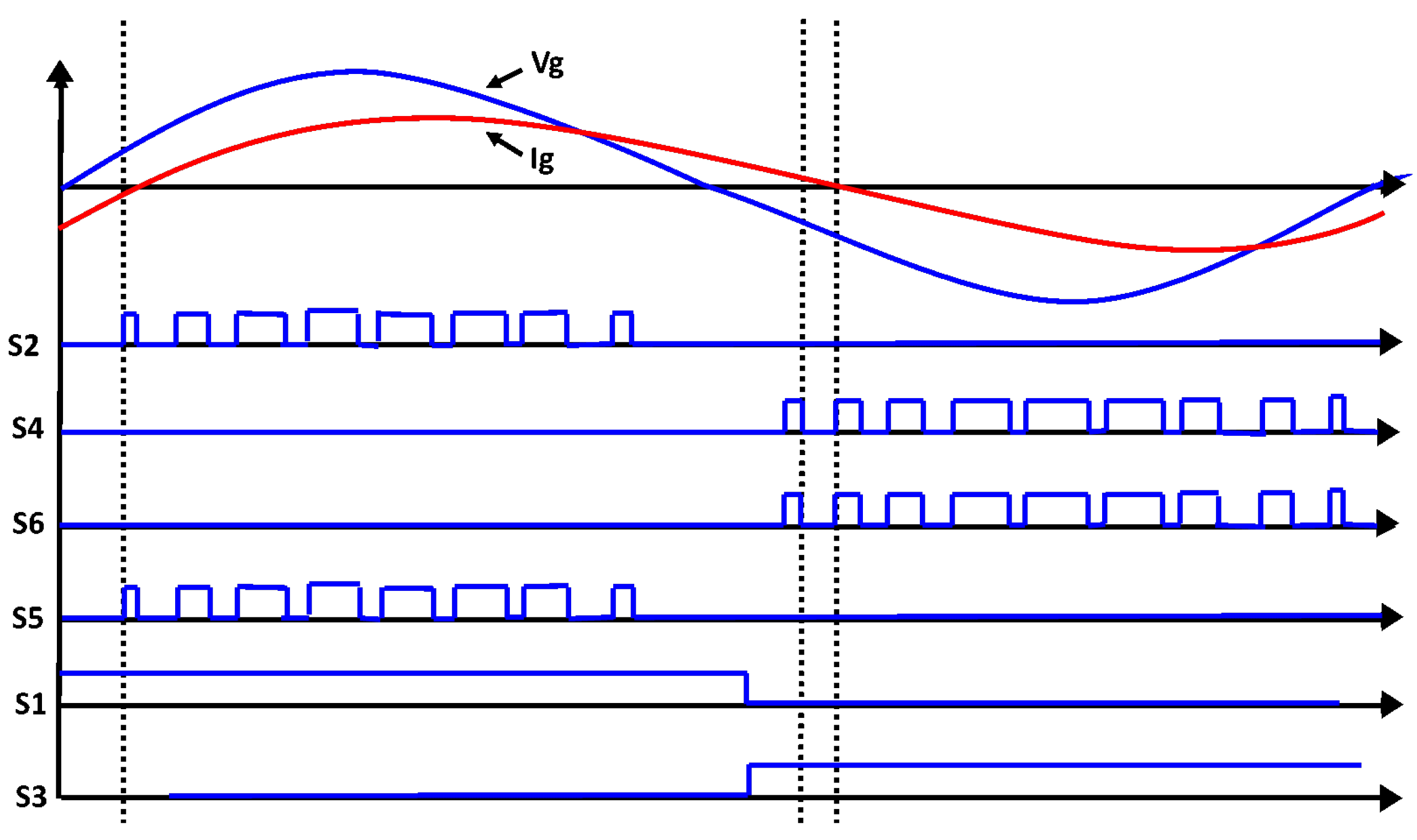
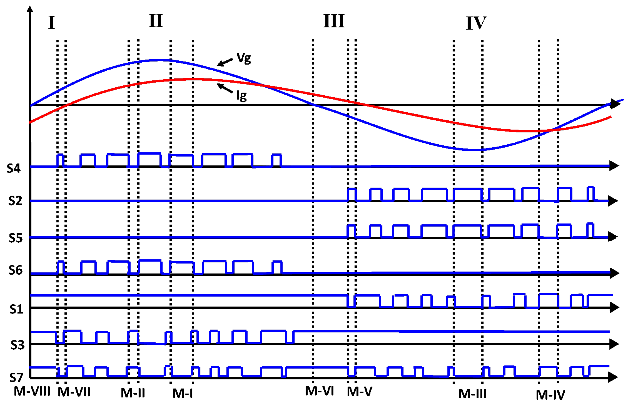
3. Modulation Technique for Reactive Power Generation

The proposed PWM technique is divided into four regions and eight modes, as shown in Figure 5. In Regions II and IV, the power is positive where I g and V g have the same polarity. The power is negative in Regions I and III where I g and V g have an opposite sign. The operation modes are described as follows.
Mode-I is the active mode in the positive power region (both I g and V g are positive). In this mode, S1, S6 and S4 are turned ON, and the other switches are turned OFF, as shown in Figure 6a. The inductor current is flowing through S4 and S6. Even though S3 is turned ON, there is no current flowing through it, which means that the S1 switch has no conduction loss in this mode. The common mode voltage in Mode-I is calculated as follows:
v A N = U P V
v B N = 0
v C M = v A N + v B N 2 = 0.5 U P V
Mode-II is the freewheeling mode in the positive power region (both I g and V g are positive). In this mode, S1, S3 and S7 are turned ON and the other switches are turned OFF, as shown in Figure 6b. The inductor current is flowing through S1 and the antiparallel diode of S3. The common mode voltage in Mode-II is given as:
v A N = v B N = 0.5 U P V
v C M = v A N + v B N 2 = 0.5 U P V
Mode-III is the active mode in the positive power region (both I g and V g are negative). In this mode, S5, S3 and S2 are turned ON and the other switches are turned OFF, as shown in Figure 7a.
The inductor current is flowing through S2, S3 and S5. The common mode voltage in Mode-III is expressed as:
v A N = 0
v B N = U P V
v C M = v A N + v B N 2 = 0.5 U P V
Mode-IV is the freewheeling mode in the positive power region (both I g and V g are negative). In this mode, S1, S3 and S7 are turned ON, and the other switches are turned OFF, as shown in Figure 7b. The inductor current is flowing through S3 and the antiparallel diode of S1. The common mode voltage in Mode-IV is calculated as follows:
v A N = v B N = 0.5 U P V
v C M = v A N + v B N 2 = 0.5 U P V
Mode-V is the active mode in the negative power region ( I g is positive and V g is negative). In this mode S4 and S6 are OFF, while S2, S5 and S3 are ON; thus, inductor current freewheels through the anti-parallel diodes of S2, S5 and S3, as given in Figure 8a where V A N = 0 and V B N = V D C ; thus, V C M and V D M are determined as:
v D M = v A B = U P V
v C M = v A N + v B N 2 = 0.5 U P V
Mode-VI is the freewheeling mode in the negative power region ( I g is positive and V g negative). In this mode, S1 commutates complementarily to S2 and S5 at the switching frequency instead of being OFF for the whole negative period as in the conventional unipolar PWM. In this arrangement, a new current path is created to generate zero-voltage by turning OFF S2, S4, S5 and S6 and turning ON S1, S3 and S7. Thus, the inductor current passes over S1 and the antiparallel diode of S3 as depicted in Figure 8b, where V A N = V D C / 2 and V B N = V D C / 2 ; thus, V C M and V D M are determined as:
v D M = v A B = 0
v C M = v A N + v B N 2 = 0.5 U P V
Mode-VII is the active mode in the negative power region (Ig is negative and Vg is positive). In this mode, S2, S5 and S3 are OFF, while S4, S6 and S1 are ON; thus, inductor current freewheels through the anti-parallel diodes of S4 and S6, as shown in Figure 9a, where V A N = V D C and V B N = 0 ; thus, V C M and V D M are determined as:
v D M = v A B = U P V
v C M = v A N + v B N 2 = 0.5 U P V
Mode VIII is the freewheeling mode in the negative power region (Ig is negative and Vg is positive). In this mode, S3 commutates complementarily to S4 and S6 at the switching frequency instead of being OFF for the whole positive period, as in the conventional unipolar PWM. In this arrangement, a new current path is created to generate zero-voltage by turning OFF S2, S4, S5 and S6 and turning ON S1, S3 and S7. Thus, the inductor current passes over S3 and the antiparallel diode of S1 as depicted in Figure 9b, where V A N = V D C / 2 and V B N = V D C / 2 ; thus, V C M and V D M are determined as:
v D M = v A B = 0
v C M = v A N + v B N 2 = 0.5 U P V
By implementing the proposed modulation, a new current path is created in Regions I and III to achieve a zero-voltage state. Therefore, the three output voltages are generated + V D C , zero and V D C , which satisfy the principle operation of the unipolar PWM technique. The main concept of the proposed modulation technique is to create a bidirectional current path of S1 and S3 during the negative power region. As a result, reactive power generation can be achieved with the proposed modulation technique. Moreover, the proposed modulation technique maintains a constant common mode voltage at V D C / 2 over all the operation modes, which will result in eliminating leakage current. Consequently, the proposed H6 topology with the modified unipolar PWM technique is suitable for the next generation of PV transformerless inverter applications.

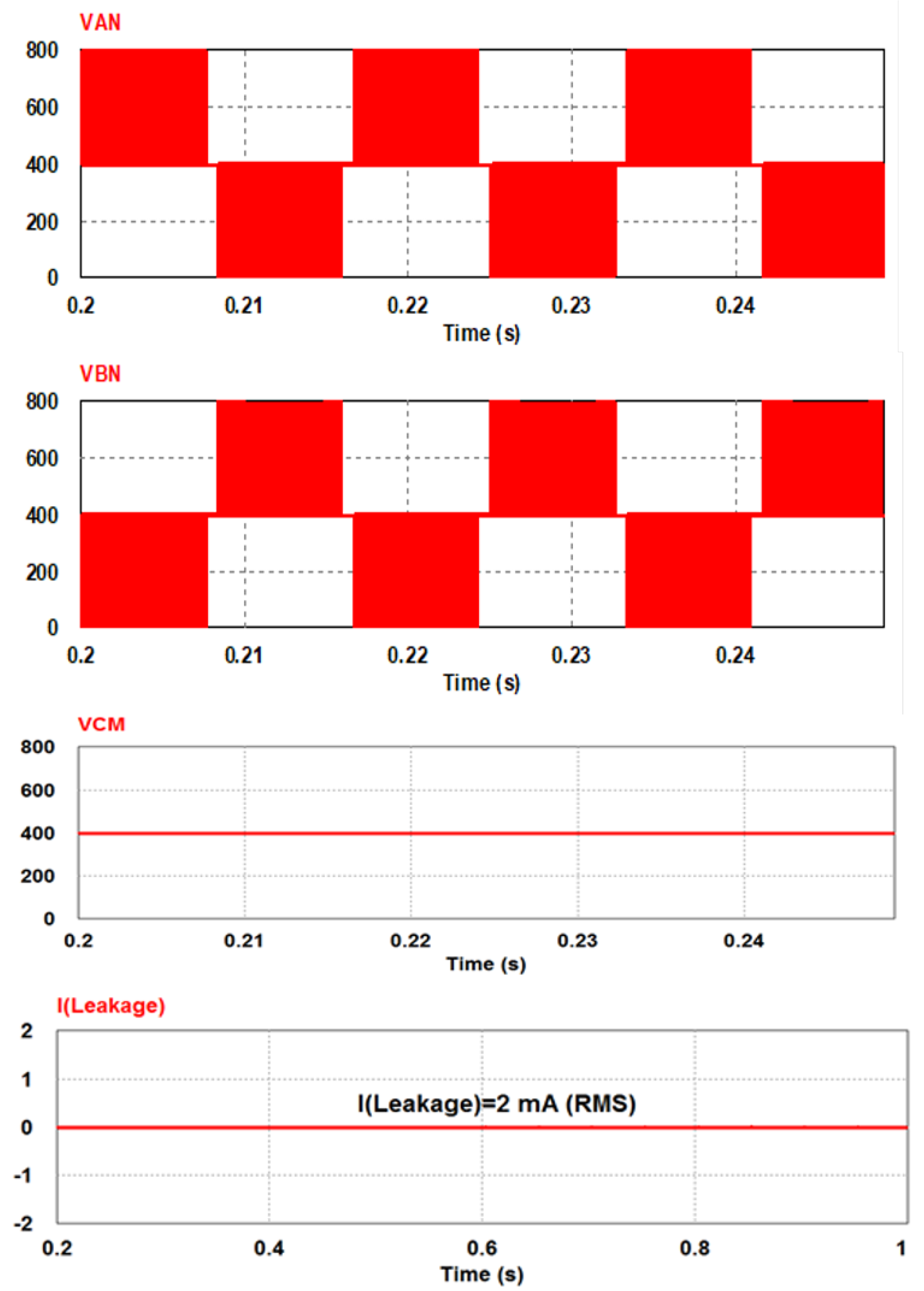
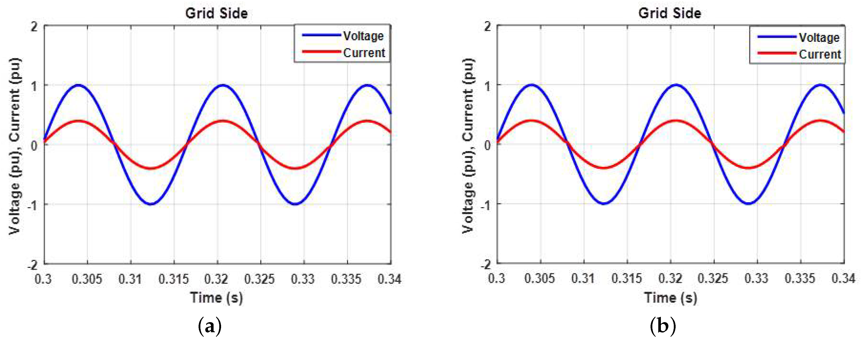
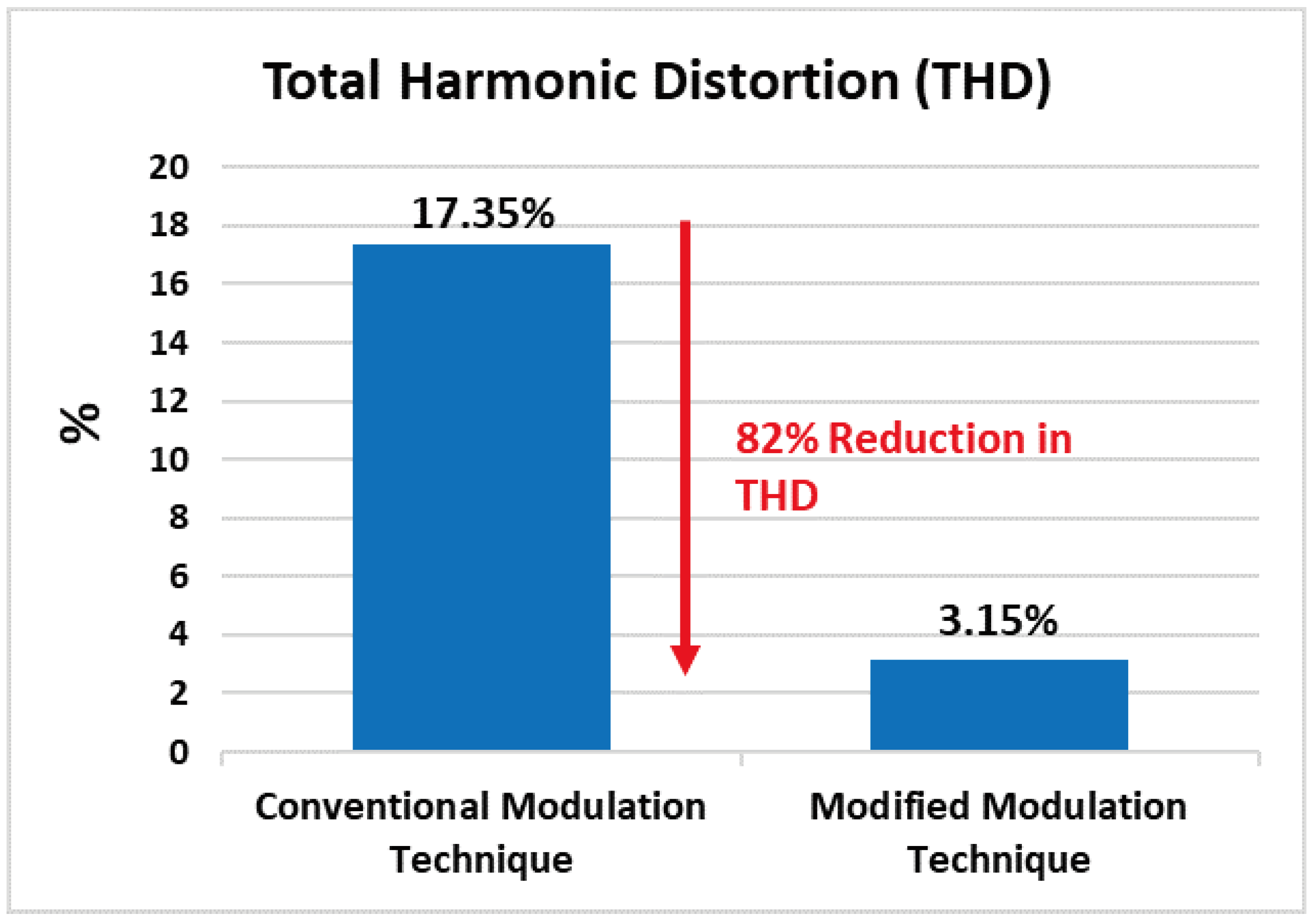
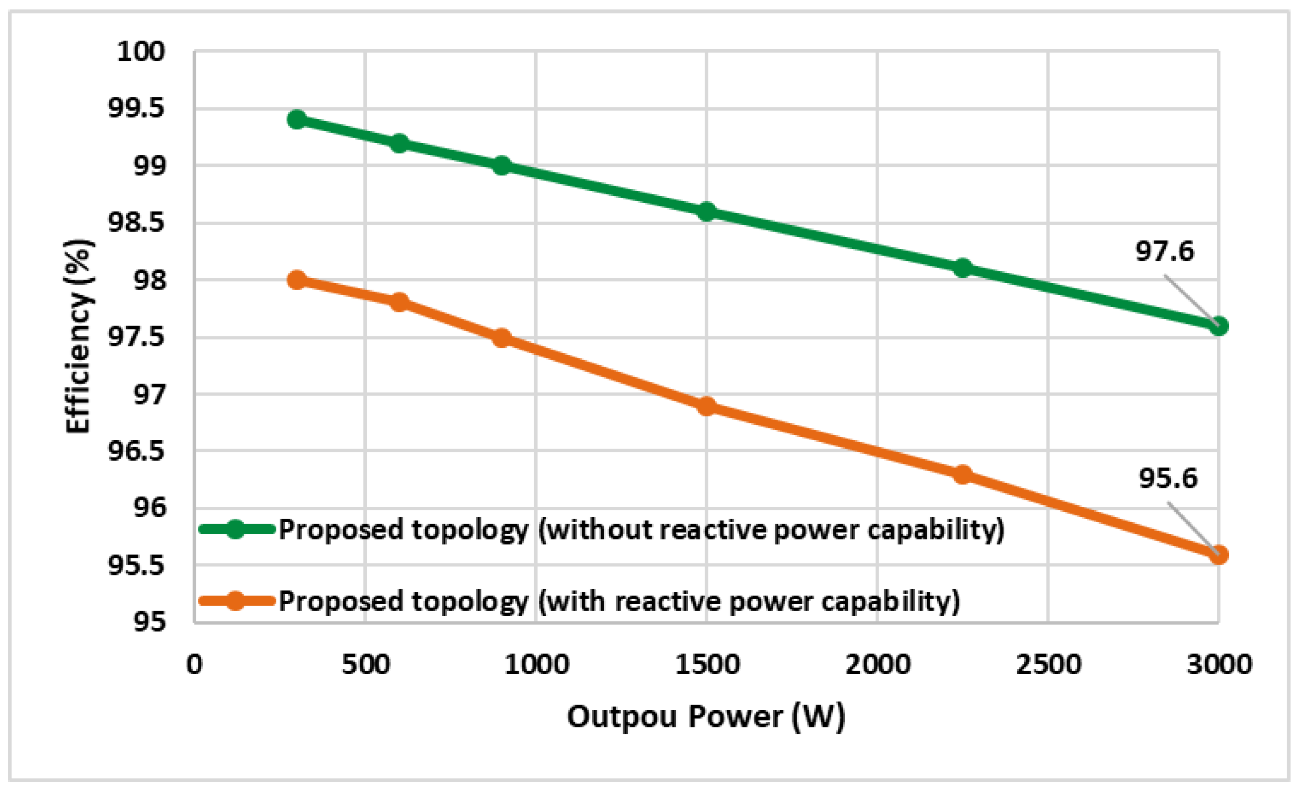
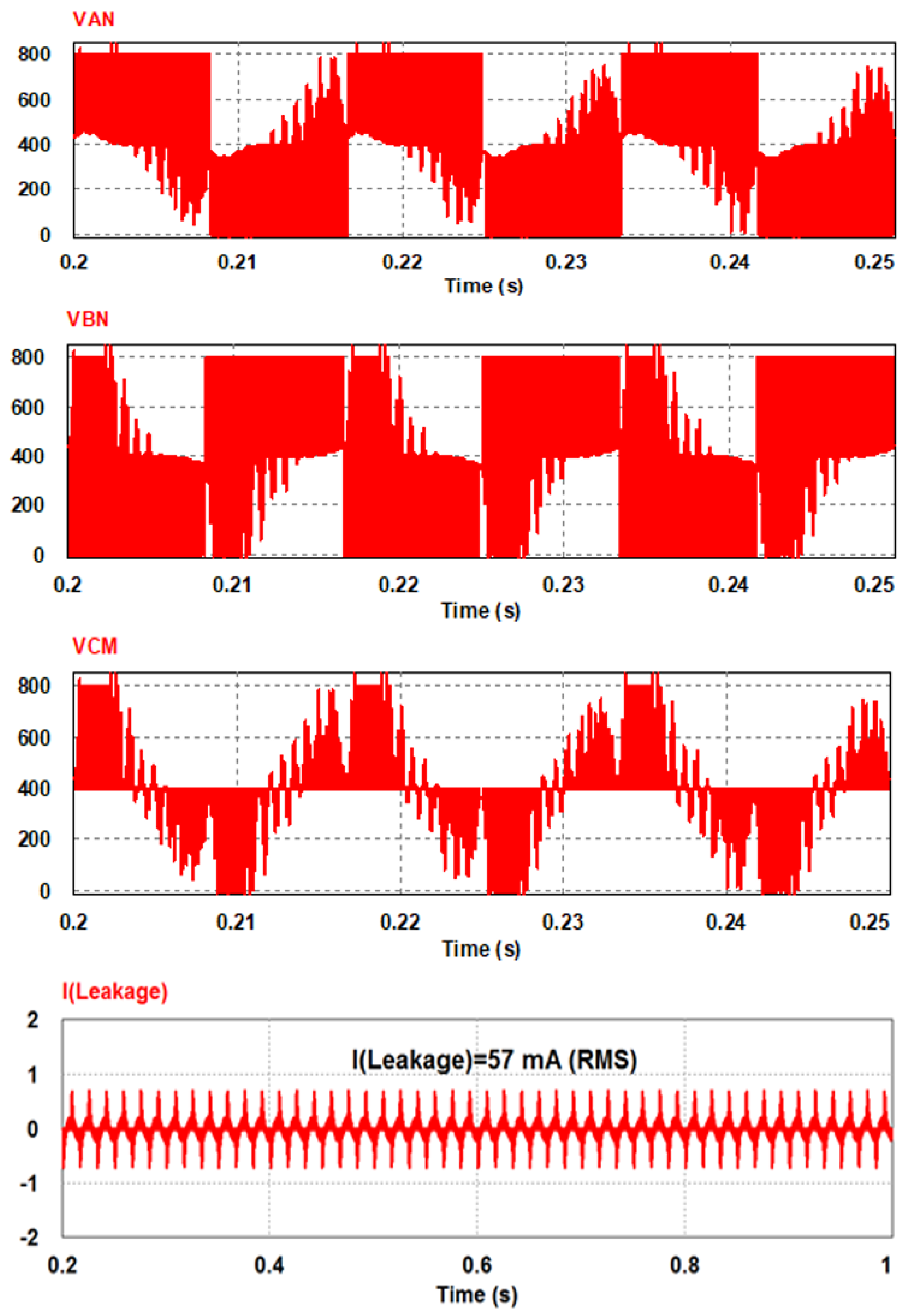
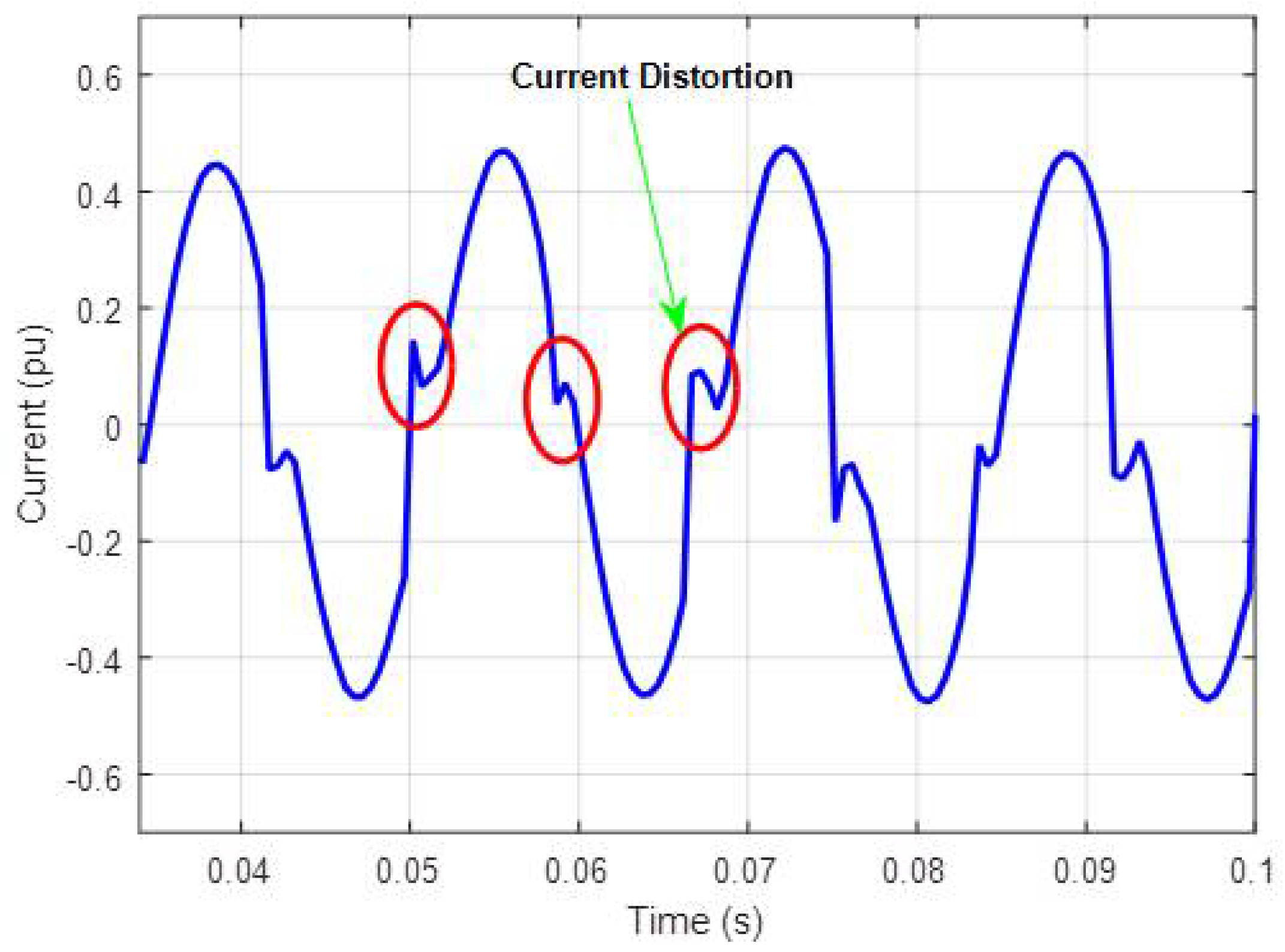
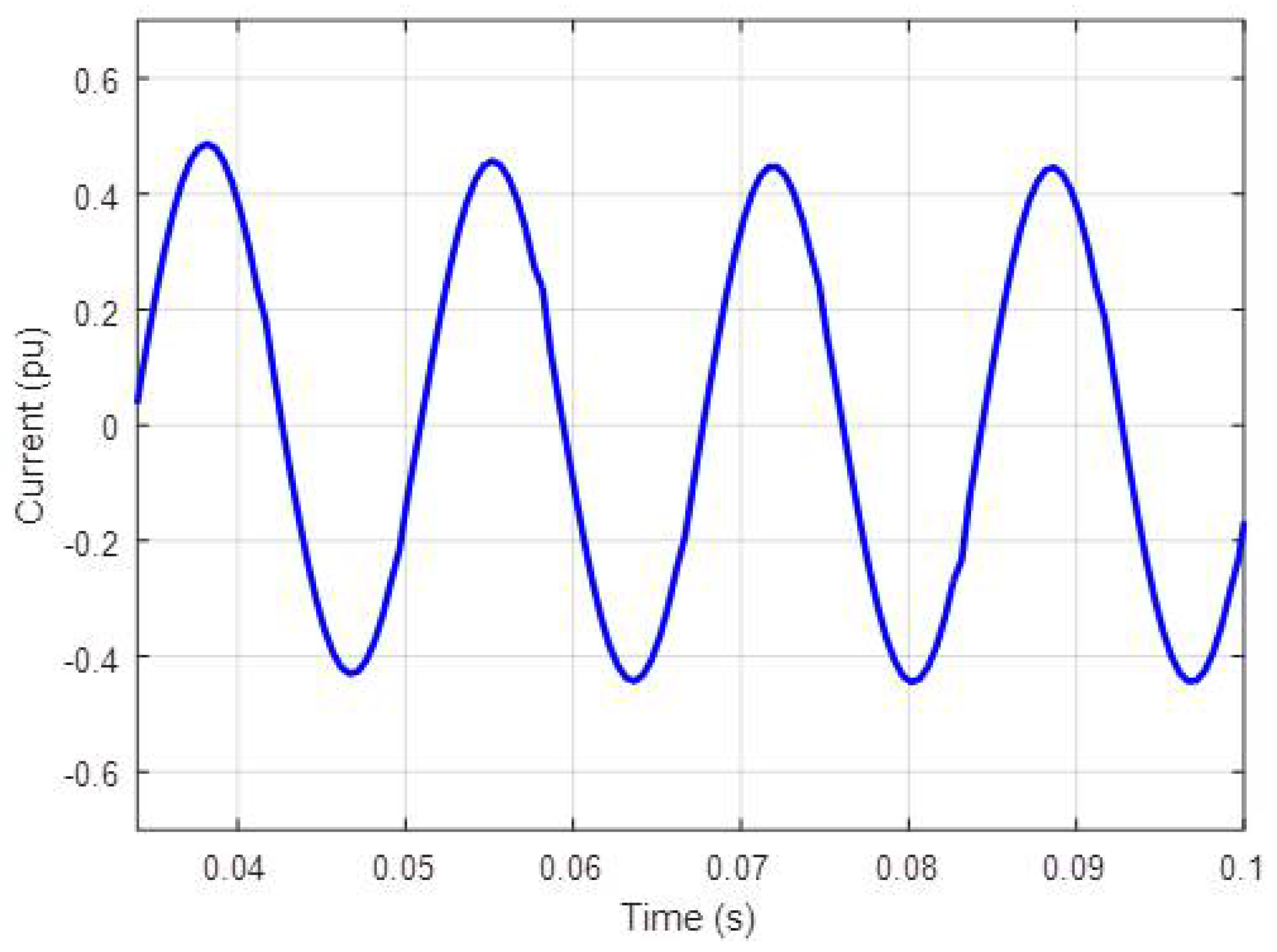
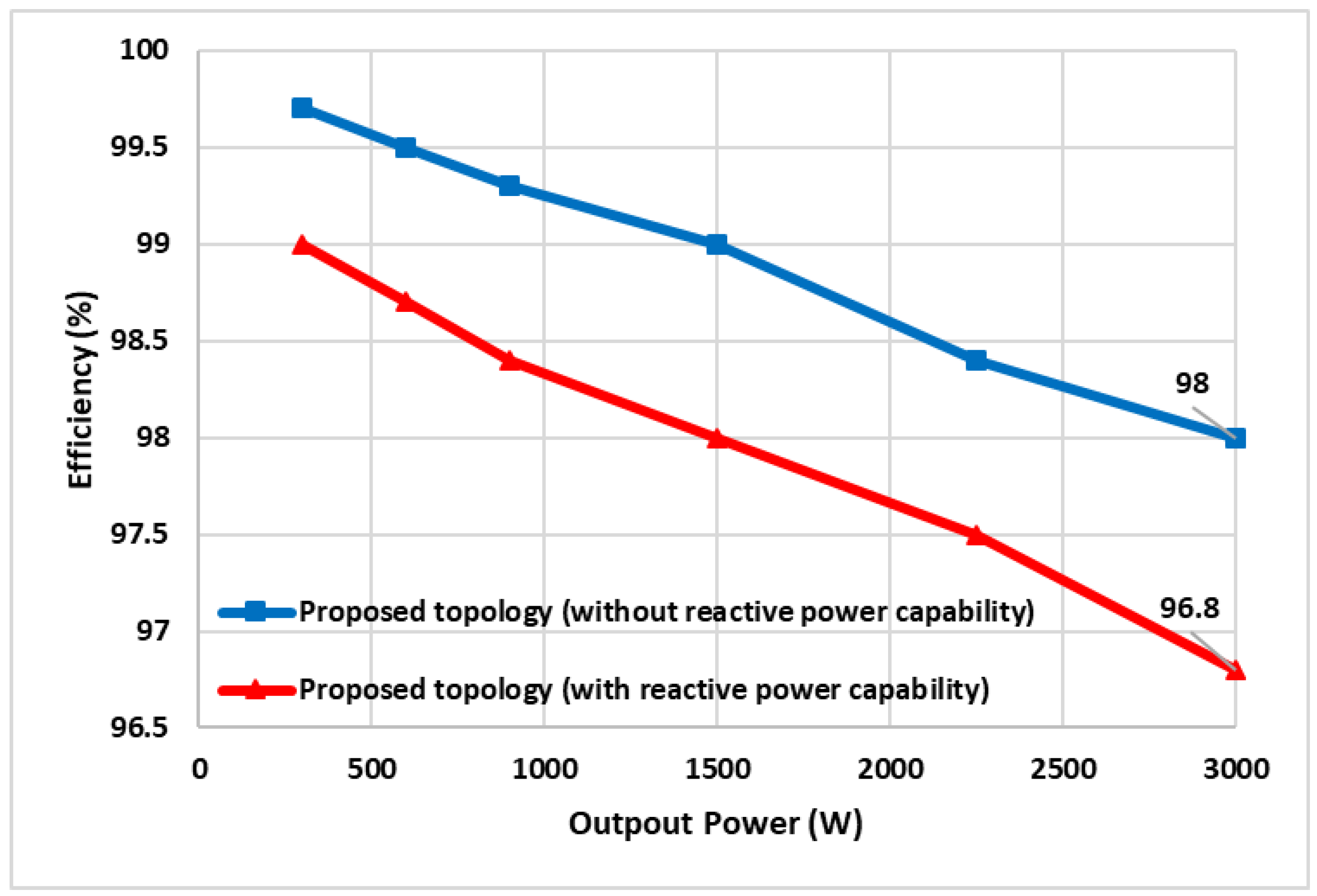
4. Simulation Results

PSIM and MATLAB/SIMULINK simulation software programs were used to design the proposed topology to evaluate its performance. The parameters of the system design are shown in Table 1. The simulation included two switching frequencies: 16 kHz and 100 kHz.
The CM characteristics of the proposed topology, with only galvanic isolation, are given in Figure 10.
It is observed that the voltage waveforms of V A N and V B N are oscillating. Furthermore, the common mode voltage V C M is oscillating and not constant at 400 V. Therefore, there is a flow of leakage current that cannot be eliminated. To resolve this problem, the proposed topology is modified with a clamping method and the CM characteristics, such as V A N , V B N , V C M and leakage, that are shown in Figure 11. It is also noted that the voltage waveforms of V A N and V B N are smooth and complementary to each other. As a result, the V C M is totally clamped to 400 V over the whole period, which will lead to a total elimination of leakage current.
The simulated waveform of the proposed H6 inverter at unity power factor with the traditional and proposed unipolar PWM is presented in Figure 12. Both modulation techniques are expected to perform properly for purely active power of a unity power factor. On the other hand, with the non-unity power factor (reactive power generation), the traditional unipolar PWM does not work correctly.
Figure 13 shows a current distortion in the negative power region because there is no current path to realize a zero-voltage through the negative power region. However, the issue of current distortion with conventional unipolar PWM can be resolved with the proposed unipolar PWM. The proposed modulation technique works optimally with a lagging or leading power factor where the simulated waveform has free current distortion as depicted in Figure 14. Hence, the proposed modulation technique supports the proposed H6 inverter for reactive power generation.
It is noted that the proposed topology with the modified modulation method succeeded in handling reactive power with 3.15% THD, as shown in Figure 15. However, the proposed topology incorporating the conventional modulation method generates high THD that does not comply with the IEEE 1547 Standard (THD < 5%) due to the absence of current path in the negative power region. The THD is reduced by 82% with the modified modulation. The efficiency of the proposed topology with and without reactive power capability is measured with SiC MOSFET switching devices. The efficiency is determined according to the California Energy Commission (CEC), as shown in the following:
η C E C = 0.04 η 10 % + 0.05 η 20 % + 0.12 η 30 % + 0.21 η 50 % + 0.53 η 75 % + 0.05 η 100 %
Two switching frequencies using 16 kHz and 100 kHz and the calculated efficiency are given on Table 2 and Table 3. The efficiency of the proposed inverter without reactive power capability at 16 kHz and 100 kHz is 98% and 97.6%, respectively. On the other hand, the efficiency of the proposed inverter with reactive power capability at 16 kHz and 100 kHz is 96.8% and 95.6%, respectively. These items are presented in Figure 16 and Figure 17. Therefore, the cost of adding reactive power capability to the proposed inverter requires a reduction in system efficiency of about 1.2% and 2% for 16 kHz and 100 kHz, respectively. This reduction of system efficiency is due to the bidirectional flow of the current during reactive power generation, which leads to an increase in conduction loss.

5. Conclusions

When operating at high switching frequency, the stray capacitors will be charged and discharged by the common mode voltage (CMV). As a result, a resonant circuit is formed that includes PV stray capacitors, grid impedance and output filter inductances. Therefore, the resonant circuit will be excited and the leakage current will flow through the parasitic capacitances between the PV panel and the ground. There are many disadvantages associated with the circulating of leakage current in the system, such as increased system losses, total harmonic distortion (THD) and serious safety and radiated interference problems. In this paper, a proposed topology is modified with an extra switch to achieve constant common mode voltage and eliminating leakage current. Moreover, the modulation method is modified so that reactive power generation can be achieved. Three voltages’ states must be generated in the negative power region to satisfy the requirement of unipolar PWM. However, conventional unipolar PWM cannot generate a zero-voltage in the negative power region. The proposed modulation technique helps to create a new current path in the negative power region where a zero-voltage state can be achieved. To this end, the proposed modulation technique enables the proposed inverter with reactive power generation without any changes to the inverter structure. Moreover, the proposed modulation achieved a constant common mode voltage that leads to eliminating leakage current. The results show that the proposed topology with the galvanic isolation method alone cannot completely eliminate leakage current. On the other hand, the common mode voltage is completely clamped at 400 V during the entire period, and a complete elimination of leakage current is achieved with the modified proposed topology. Moreover, there is current distortion in the negative power region with conventional PWM, while with the proposed modulation, a current path is created and the current distortion is eliminated. Furthermore, THD is reduced by 82% with the modified modulation method. The efficiency of the system is measured with SiC MOSFET to enhance system performance, especially with reactive power generation. It is observed that system efficiency decreased by 2% at 100 kHz due to the reactive power capability, because the increase in conducting switches also increases loss. In brief, the proposed modulation technique satisfies the requirement for a next-generation, single-phase, PV grid tied inverter where reactive power control is required.

Author Contributions

F.A. conceived of and organized this work. He also performed the energy and power simulations in the software PowerSim and MATLAB/Simulink and acquired and analyzed the data. M.M. provided the technical feedback and revised the manuscript. The manuscript was written by F.A. All authors proofread the manuscript.

Funding

This research received no external funding.

Conflicts of Interest

The authors declare no conflict of interest.

References

  1. Li, W.; Gu, Y.; Luo, H.; Cui, W.; He, X.; Xia, C. Topology review and derivation methodology of single-phase transformerless photovoltaic inverters for leakage current suppression. IEEE Trans. Ind. Electron. 2015, 62, 4537–4551. [Google Scholar] [CrossRef]
  2. Guo, X.; He, R.; Jian, J.; Lu, Z.; Sun, X.; Guerrro, M. Leakage current elimination of four-leg inverter for transformerless three-phase PV systems. IEEE Trans. Power Electron. 2016, 31, 1841–1846. [Google Scholar] [CrossRef]
  3. Kerekes, T.; Teodorescu, R.; Rodríguez, P.; Vázquez, G.; Aldabas, E. A new high-efficiency single-phase transformerless PV inverter topology. IEEE Trans. Ind. Electron. 2011, 58, 184–191. [Google Scholar] [CrossRef] [Green Version]
  4. Dutta, S.; Debnath, D.; Chatterjee, K. A grid-connected single-phase transformerless inverter controlling two solar PV arrays operating under different atmospheric conditions. IEEE Trans. Ind. Electron. 2018, 65, 374–385. [Google Scholar] [CrossRef]
  5. Knabben, G.C.; Schmitz, L.; Coelho, R.F.; Martins, D.C.; Custódio, O.J.; de Medeiros, R.Z.; Bettiol, A.L. Transformerless micro-inverter for grid-connected photovoltaic systems. In Proceedings of the 52nd International Universities Power Engineering Conference (UPEC), Heraklion, Greece, 28–31 August 2017; pp. 1–6. [Google Scholar] [CrossRef]
  6. AZhao, T.; Bhavaraju, V.; Nirantare, P.; Xu, J. Evaluation of commercial scale transformerless solar inverter technology. In Proceedings of the 2015 IEEE Energy Conversion Congress and Exposition (ECCE), Montreal, QC, Canada, 20–24 September 2015; pp. 5342–5348. [Google Scholar] [CrossRef]
  7. Chen, B.; Lai, J.S. A family of single-phase transformerless inverters with asymmetric phase-legs. In Proceedings of the 2015 IEEE Applied Power Electronics Conference and Exposition (APEC), Charlotte, NC, USA, 15–19 March 2015; pp. 2200–2205. [Google Scholar] [CrossRef]
  8. Lee, J.; Lee, K. New modulation techniques for a leakage current reduction and a neutral-point voltage balance in transformerless photovoltaic systems using a three-level inverter. IEEE Trans. Power Electron. 2014, 29, 1720–1732. [Google Scholar] [CrossRef]
  9. Freddy, T.; Rahim, N.; Hew, W.; Che, H. Modulation techniques to reduce leakage current in three-phase transformerless H7 photovoltaic inverter. IEEE Trans. Ind. Electron. 2015, 62, 322–331. [Google Scholar] [CrossRef]
  10. Cha, W.; Kim, K.; Cho, Y.; Lee, S.; Kwon, B. Evaluation and analysis of transformerless photovoltaic inverter topology for efficiency improvement and reduction of leakage current. IET Power Electron. 2014, 8, 255–267. [Google Scholar] [CrossRef]
  11. Ardashir, F.; Siwakoti, P.; Sabahi, M.; Hosseini, S.; Blaabjerg, F. S4 grid-connected single-phase transformerless inverter for PV application. In Proceedings of the IECON 2016—42nd Annual Conference of the IEEE Industrial Electronics Society, Florence, Italy, 3–26 October 2016; pp. 2384–2389. [Google Scholar]
  12. Gotekar, P.; Muley, S.; Kothari, D.; Umre, B. Comparison of full bridge bipolar, H5, H6 and HERIC inverter for single phase photovoltaic systems—A review. In Proceedings of the 2015 Annual IEEE India Conference (INDICON), New Delhi, India, 17–20 December 2015; pp. 1–6. [Google Scholar] [CrossRef]
  13. Zhang, L.; Sun, K.; Xing, Y.; Xing, M. H6 Transformerless Full-Bridge PV Grid-Tied Inverters. IEEE Trans. Power Electron. 2014, 29, 1229–1238. [Google Scholar] [CrossRef]
  14. Yang, Y.; Blaabjerg, F.; Wang, H. Low-voltage ride-through of single-phase transformerless photovoltaic inverters. IEEE Trans. Ind. Appl. 2014, 50, 1942–1952. [Google Scholar] [CrossRef]
  15. Wu, T.; Kuo, C.; Sun, K.; Hsieh, H. Combined unipolar and bipolar PWM for current distortion improvement during power compensation. IEEE Trans. Power Electron. 2013, 29, 1702–1709. [Google Scholar] [CrossRef]
  16. Bojoi, R.; Limongi, L.; Roiu, D.; Tenconi, A. Enhanced Power Quality Control Strategy for Single-Phase Inverters in Distributed Generation Systems. IEEE Trans. Power Electron. 2011, 26, 798–806. [Google Scholar] [CrossRef]
  17. Zong, X. A Single Phase Grid Connected DC/AC Inverter with Reactive Power Control for Residential PV Application. Master’s Dissertation, University of Toronto, Toronto, ON, USA, 2011. Available online: https://tspace.library.utoronto.ca/bitstream/1807/31665/1/Zong_Xiangdong_201111_MASC_thesis.pdf (accessed on 11 March 2018).
  18. Chen, B.; Gu, B.; Zhang, L.; Lai, J. A novel pulse-width modulation method for reactive power generation on a CoolMOS-and SiC-diode-based transformerless inverter. IEEE Trans. Ind. Electron. 2016, 63, 1539–1548. [Google Scholar] [CrossRef]
  19. Islam, M.; Afrin, N.; Mekhilef, S. Efficient single-phase transformerless inverter for grid-tied PVG system with reactive power control. IEEE Trans. Sustain. Energy. 2016, 7, 1205–1215. [Google Scholar] [CrossRef]
  20. Jahdi, S.; Alatise, O.; Bonyadi, R.; Alexakis, P.; Fisher, C.A.; Gonzalez, J.A.O.; Ran, L.; Mawby, P. An Analysis of the Switching Performance and Robustness of Power MOSFETs Body Diodes: A Technology Evaluation. IEEE Trans. Power Electron. 2015, 30, 2383–2394. [Google Scholar] [CrossRef] [Green Version]
  21. Chen, B.; Gu, B.; Zhang, L.; Zahid, Z.U.; Lai, J.S.J.; Liao, Z.; Hao, R. A high-efficiency MOSFET transformerless inverter for nonisolated microinverter applications. IEEE Trans. Power Electron. 2015, 30, 3610–3622. [Google Scholar] [CrossRef]
  22. Castellazzi, A.; Fayyaz, A.; Romano, G.; Riccio, M.; Irace, A.; Urresti-Ibanez, J.; Wright, N. Transient out-of-SOA robustness of SiC power MOSFETs. Proceeings of the 2017 IEEE International Reliability Physics Symposium (IRPS), Monterey, CA, USA, 2–6 April 2017. [Google Scholar] [CrossRef]
  23. Jordan, J.; Esteve, V.; Sanchis-Kilders, E.; Dede, E.J.; Maset, E.; Ejea, J.B.; Ferreres, A. A comparative performance study of a 1200 V Si and SiC MOSFET intrinsic diode on an induction heating inverter. IEEE Trans. Power Electron. 2014, 29, 2550–2562. [Google Scholar] [CrossRef]
  24. Wang, Z.; Zhang, J.; Wu, X.; Sheng, K. Evaluation of reverse recovery characteristic of silicon carbide metal–oxide–semiconductor field-effect transistor intrinsic diode. IET Power Electron. 2016, 9, 969–976. [Google Scholar] [CrossRef]
  25. Kusumoto, O.; Ohoka, A.; Horikawa, N.; Tanaka, K.; Niwayama, M.; Uchida, M.; Kanzawa, Y.; Sawada, K.; Ueda, T. Reliability of Diode-Integrated SiC Power MOSFET(DioMOS). Microelectron. Reliab. 2016, 58, 158–163. [Google Scholar] [CrossRef]
  26. Chen, K.; Zhao, Z.; Yuan, L.; Lu, T.; He, F. The Impact of Nonlinear Junction Capacitance on Switching Transient and Its Modeling for SiC MOSFET. IEEE Trans. Electron Devices 2015, 62, 333–338. [Google Scholar] [CrossRef]
  27. Fayyaz, A.; Romano, G.; Castellazzi, A. Body diode reliability investigation of SiC power MOSFETs. Microelectron. Reliab. 2016, 64, 530–534. [Google Scholar] [CrossRef] [Green Version]
  28. Wang, Z.; Ouyang, J.; Zhang, J.; Wu, X.; Sheng, K. Analysis on reverse recovery characteristic of SiC MOSFET intrinsic diode. In Proceedings of the 2014 IEEE Energy Conversion Congress and Exposition (ECCE), Pittsburgh, PA, USA, 4–18 September 2014; pp. 2832–2837. [Google Scholar] [CrossRef]
  29. Liu, H.; Wu, H.; Lu, Y.; Xing, Y.; Sun, K. A high efficiency inverter based on SiC MOSFET without externally antiparalleled diodes. In Proceedings of the 2014 IEEE Applied Power Electronics Conference and Exposition—APEC 2014, Fort Worth, TX, USA, 16–20 March 2014; pp. 163–167. [Google Scholar] [CrossRef]
  30. Hou, X.; Boroyevich, D.; Burgos, R. Characterization on latest-generation SiC MOSFET’s body diode. In Proceedings of the 2016 IEEE 4th Workshop on Wide Bandgap Power Devices and Applications (WiPDA), Fayetteville, AR, USA, 7–9 November 2016; pp. 247–252. [Google Scholar] [CrossRef]
  31. Almasoudi, F.; Alatawi, K.; Matin, M. High efficiency three level transformerless inverter based on SiC MOSFETs for PV applications. In Proceedings of the 2017 IEEE International Conference on Electro Information Technology (EIT), Lincoln, NE, USA, 14–17 May 2017; pp. 617–622. [Google Scholar] [CrossRef]
  32. Almasoudi, F.M.; Alatawi, K.S.; Matin, M. High efficiency H6 single-phase transformerless grid-tied PV inverter with proposed modulation for reactive power generation. In Proceedings of the Wide Bandgap Power Devices and Applications II, San Diego, CA, USA, 7–8 August 2017. [Google Scholar]
Figure 1. Circuit diagram of the proposed transformerless inverter topology.
Jlpea 08 00029 g001
Figure 2. Modulation strategy of the proposed transformerless inverter.
Jlpea 08 00029 g002
Figure 3. Modified proposed transformerless inverter.
Jlpea 08 00029 g003
Figure 4. Operation modes of the negative power region during freewheeling periods: (a) V g is positive and I g is negative; (b) V g is negative and I g is positive.
Jlpea 08 00029 g004
Figure 5. Modified modulation strategy for leakage current elimination and reactive power generation.
Jlpea 08 00029 g005
Figure 6. Operation modes of the proposed topology: (a) I g and V g are positive; (b) the zero state during this interval.
Jlpea 08 00029 g006
Figure 7. Operation modes of the proposed topology: (a) I g and V g are negative; (b) the zero state during this interval.
Jlpea 08 00029 g007
Figure 8. Operation modes of the proposed topology: (a) Vg is positive and Ig is negative; (b) the zero state during this interval.
Jlpea 08 00029 g008
Figure 9. Operation modes of the proposed topology: (a) V g is negative and I g is positive; (b) the zero state during this interval.
Jlpea 08 00029 g009
Figure 10. Common mode (CM) characteristics of the proposed topology.
Jlpea 08 00029 g010
Figure 11. CM characteristics of the modified topology.
Jlpea 08 00029 g011
Figure 12. V g and I g for the proposed H6 inverter with the unity power factor: (a) traditional unipolar PWM is positive; (b) proposed unipolar PWM.
Jlpea 08 00029 g012
Figure 13. Grid current for the proposed inverter with conventional unipolar PWM.
Jlpea 08 00029 g013
Figure 14. Grid current for the proposed inverter with modified conventional unipolar PWM.
Jlpea 08 00029 g014
Figure 15. Total harmonic distortion (THD) of the proposed topology with the conventional and modified modulation technique.
Jlpea 08 00029 g015
Figure 16. Efficiency of the proposed topology with SiC MOSFET at 16 kHz.
Jlpea 08 00029 g016
Figure 17. Efficiency of the proposed topology with SiC MOSFET at 100 kHz.
Jlpea 08 00029 g017
Table 1. System design parameters.
ParameterValue
Input Voltage800 V
Grid Voltage120 V
Grid Frequency60 Hz
Switching Frequency16 kHz and 100 kHz
DC Bus Capacitor ( C D C )970 μ F
Stray Parasitic Capacitance300 nF
Output Power3 kW
Table 2. SCEC efficiency of proposed topology with SiC MOSFET at 16 kHz.
Output Power300 W600 W900 W1500 W2250 W3000 WCEC
Proposed Topology (without reactive power capability)99.7%99.5%99.3%99%98.4%98%98.7%
Proposed Topology (with reactive power capability)99.2%99%98.6%98.2%97.5%96.8%97.7%
Table 3. SCEC efficiency of proposed topology with SiC MOSFET at 100 kHz.
Output Power300 W600 W900 W1500 W2250 W3000 WCEC
Proposed Topology (without reactive power capability)99.4%99.3%99%98.6%98.1%97.6%98.3%
Proposed Topology (with reactive power capability)98%97.8%97.5%96.9%96.3%95.6%96.6%

