Multi-Vdd Design for Content Addressable Memories (CAM): A Power-Delay Optimization Analysis

 ,
,
Abstract
:1. Introduction
2. Background
3. Related Work
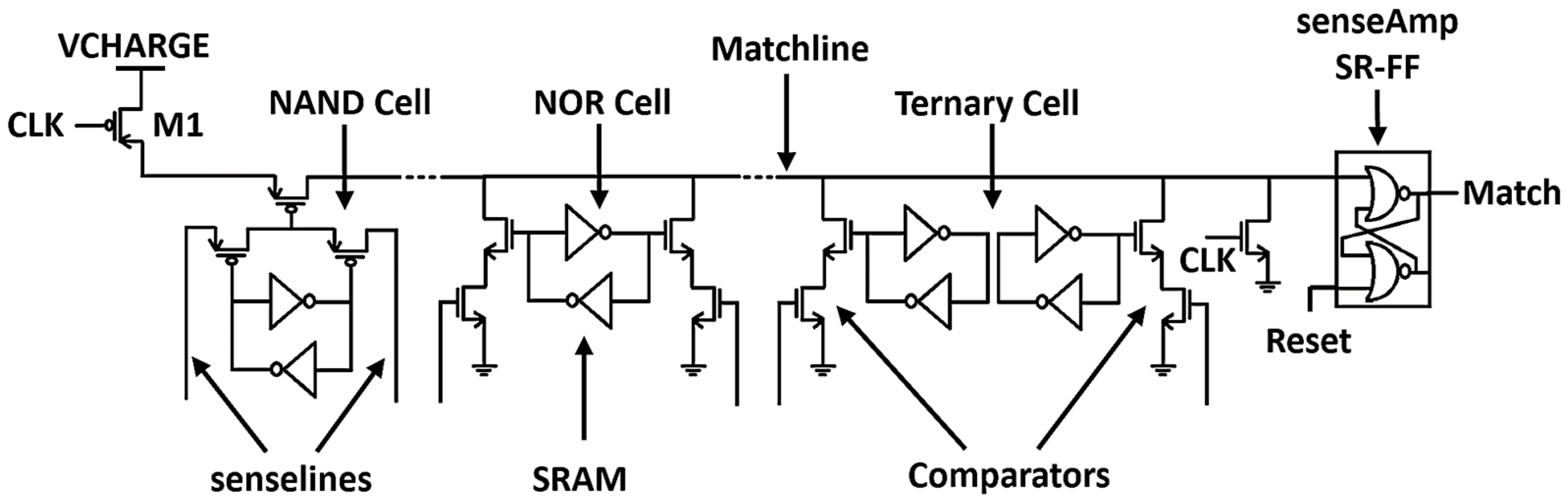
4. Multi-Vdd CAM Design
5. Power Consumption Behavior of Matchline Based Content Addressable Memories
6. Multi-Vdd CAM Behavior
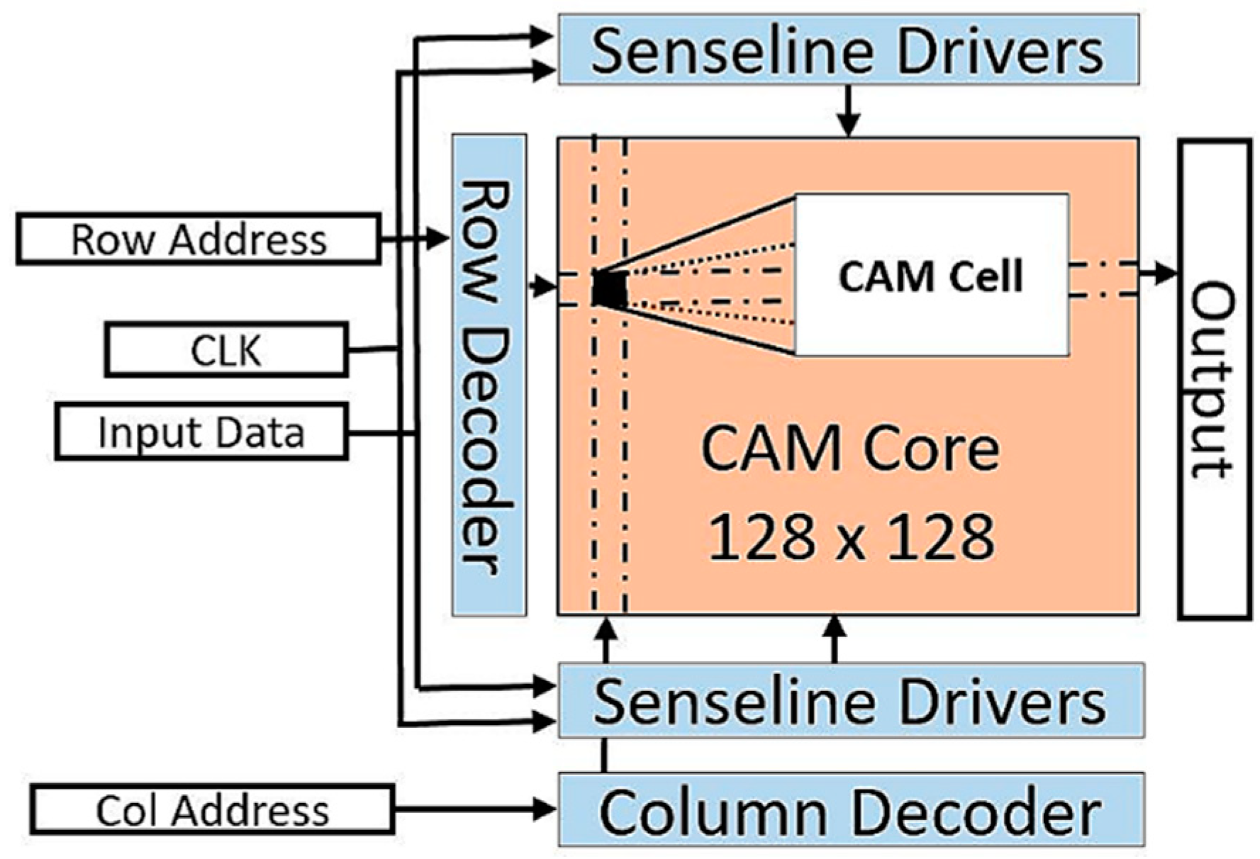
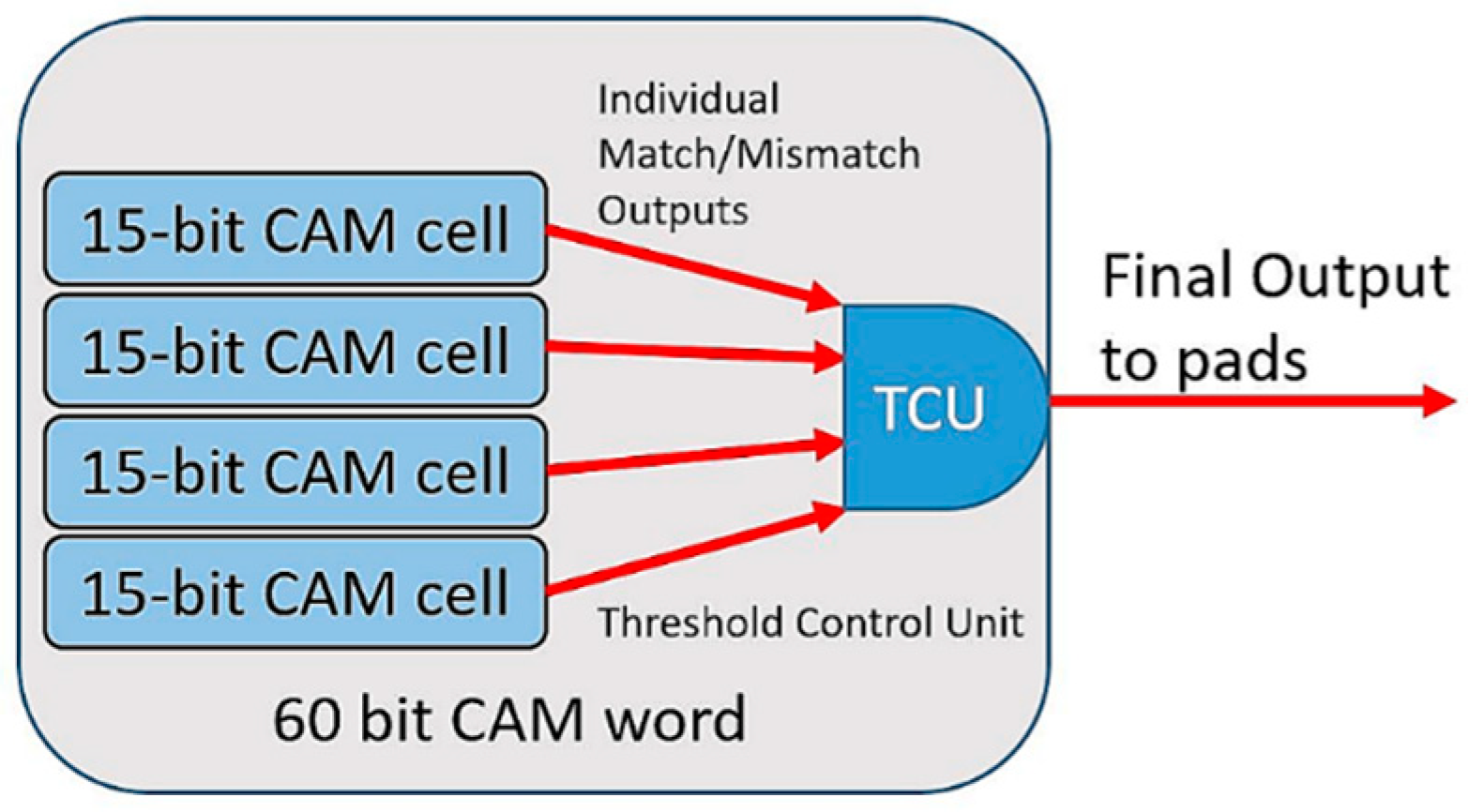
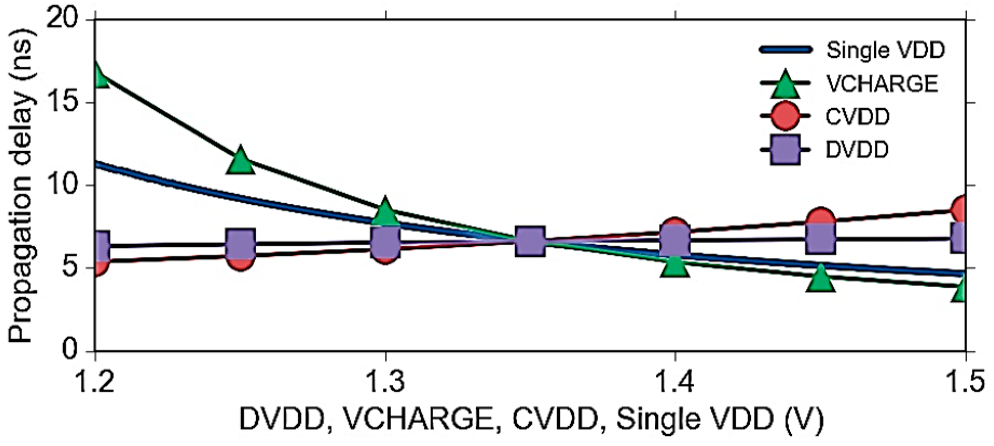
6.1. Unit CAM Cell
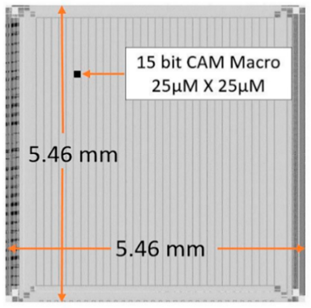
6.2. Full CAM Chip
6.3. Noise-Margin Analysis
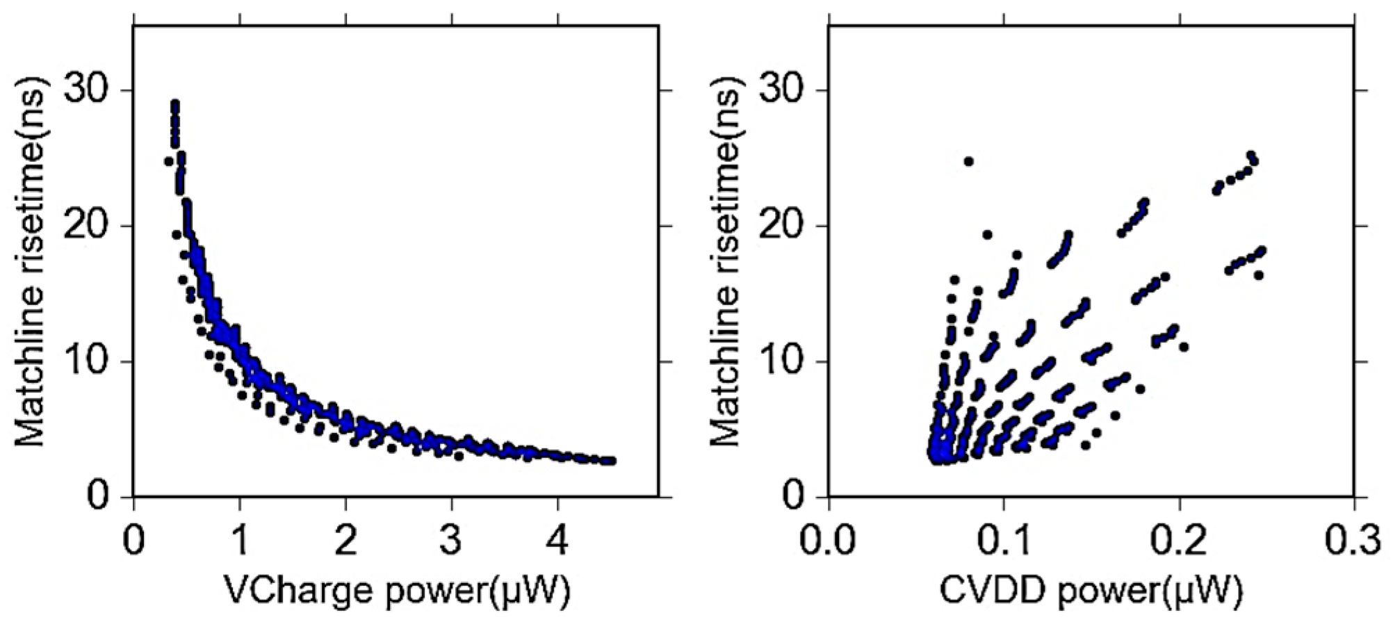
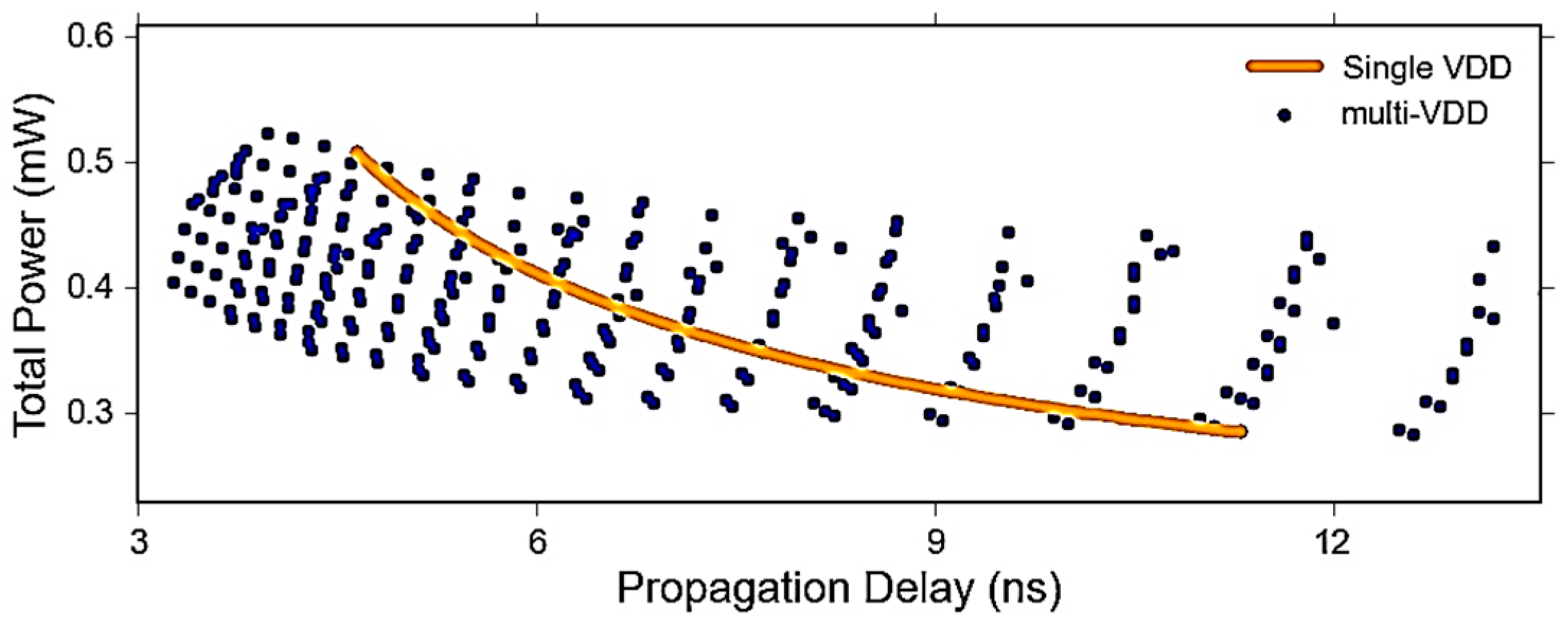
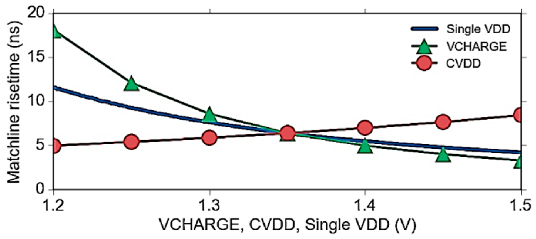
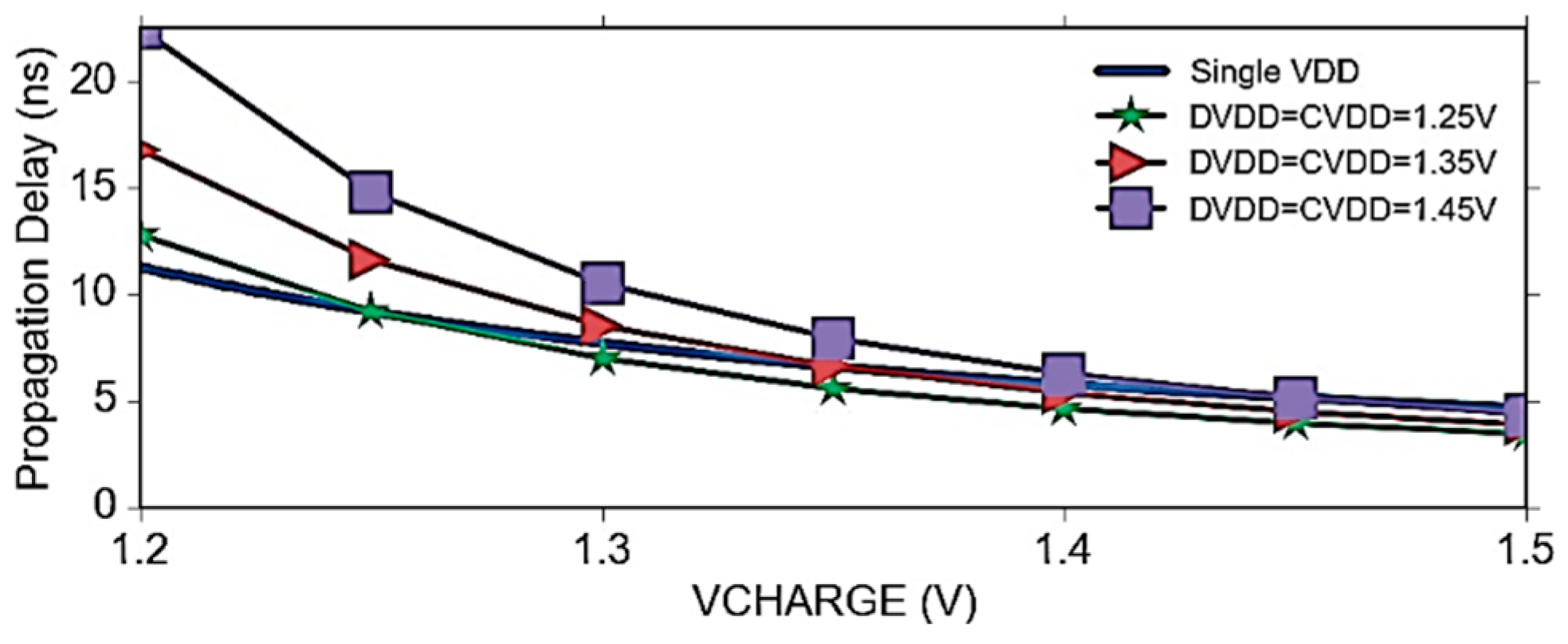
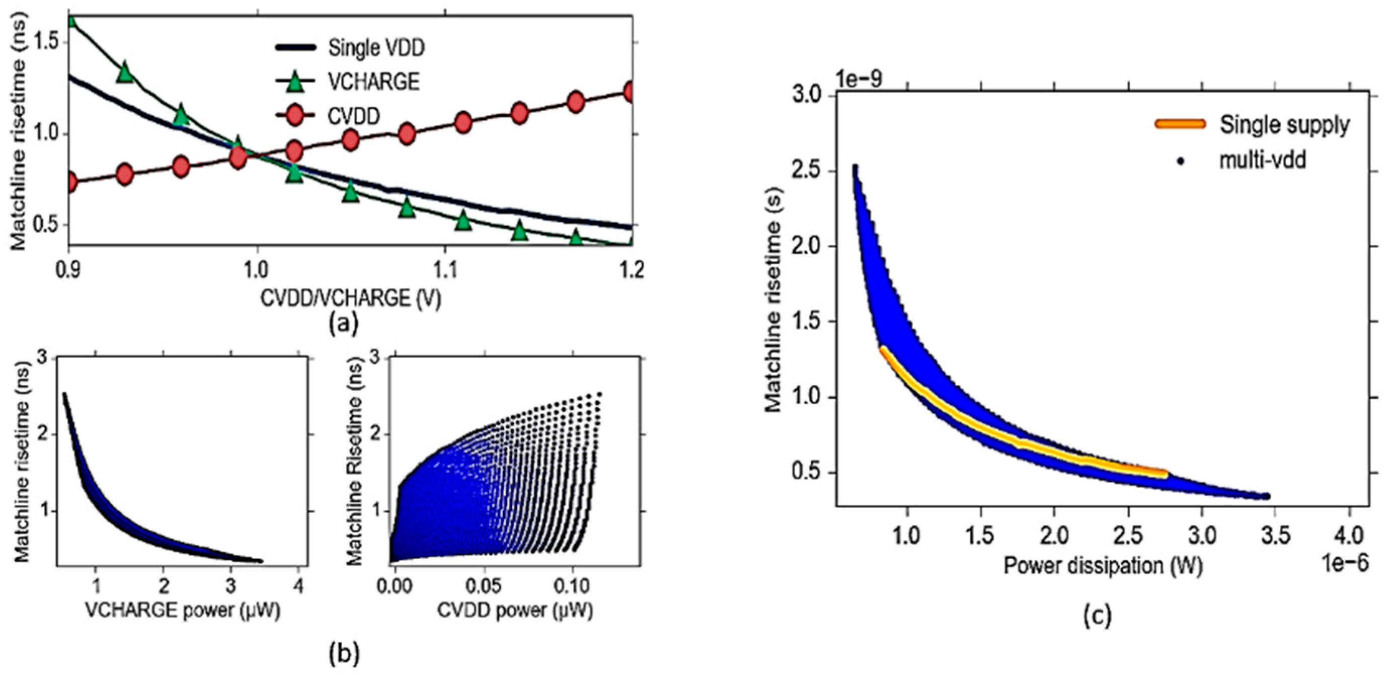
6.4. Power-Delay Optimization
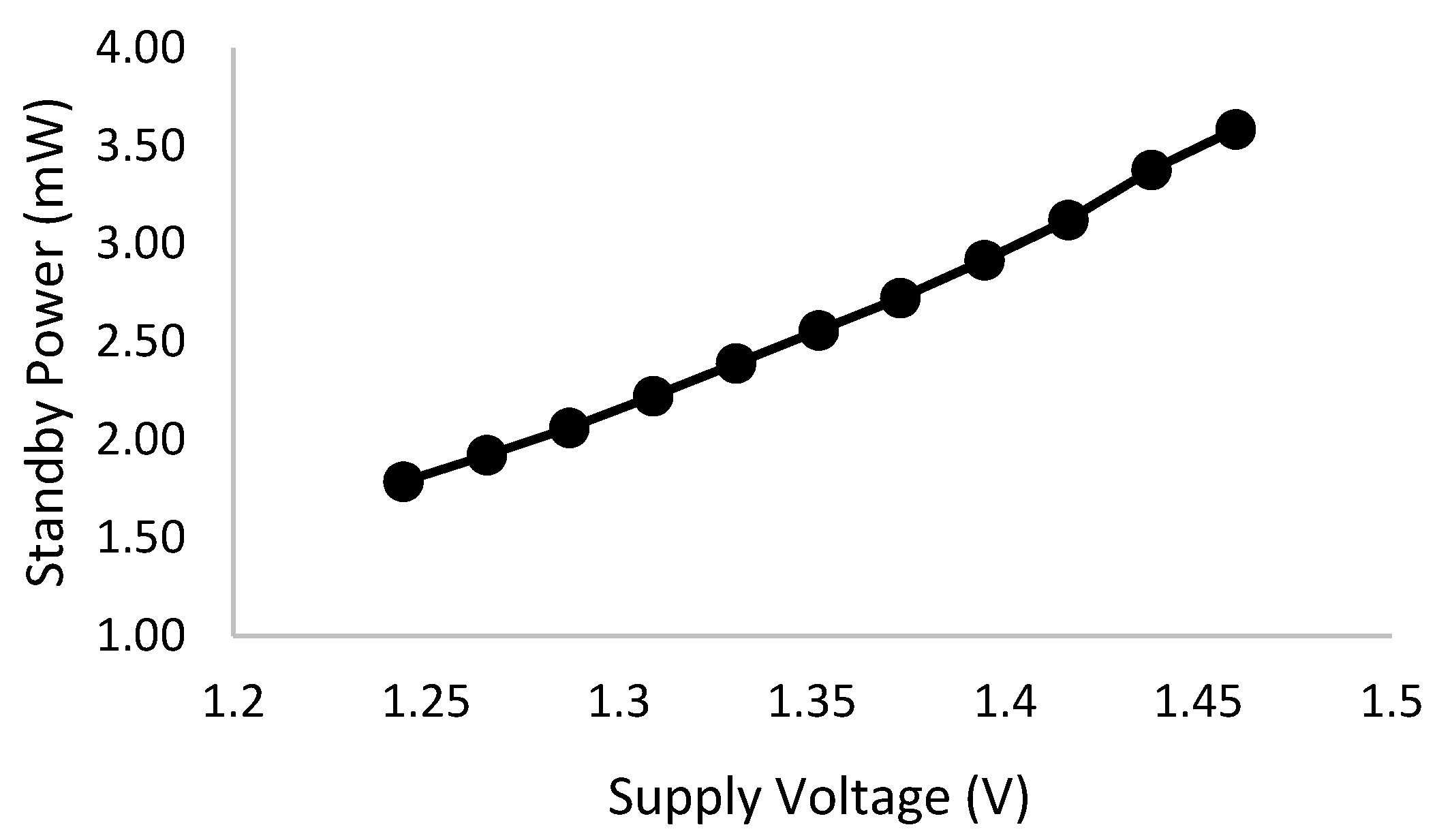
6.5. Standby Power Consumption
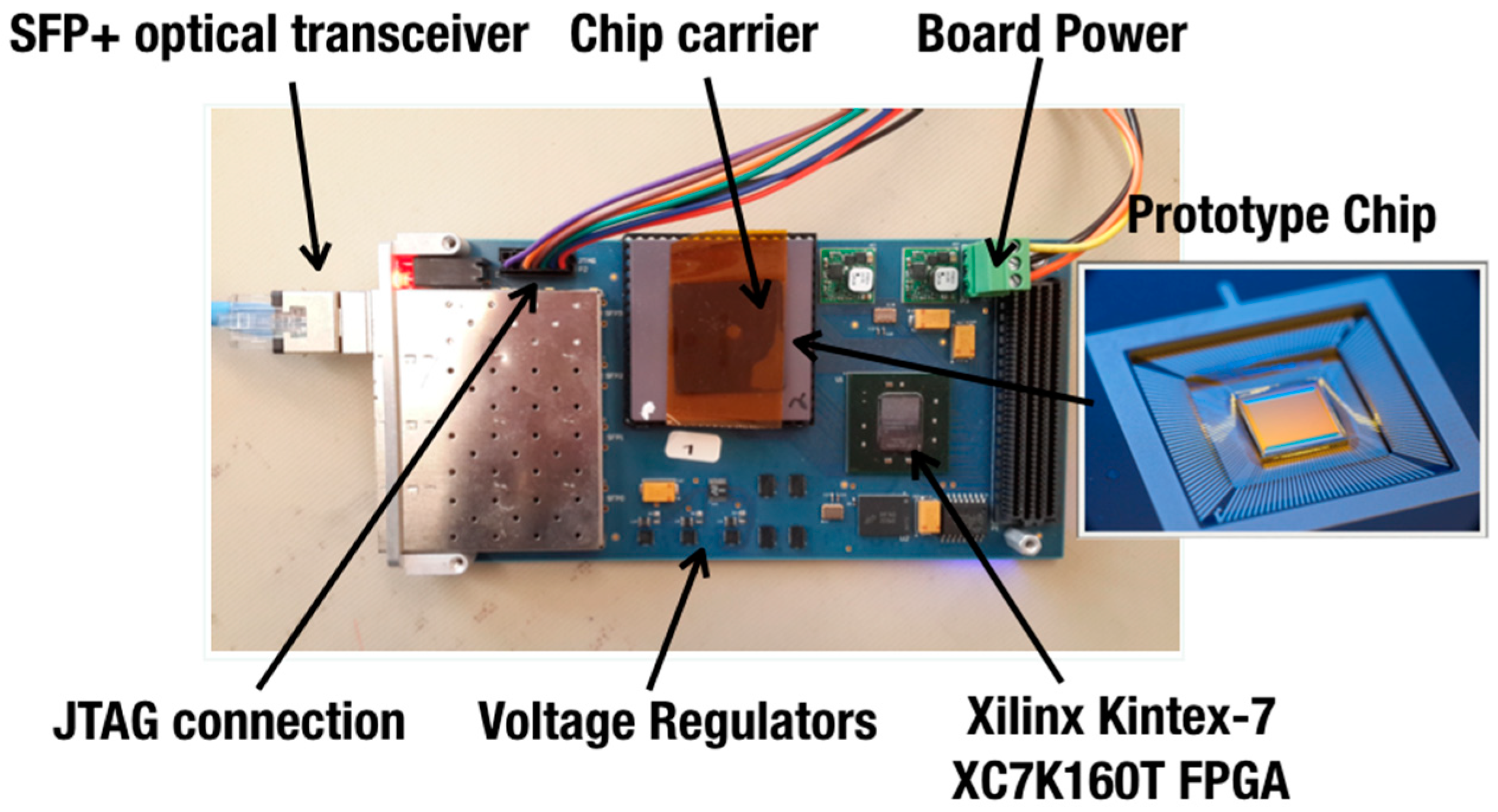
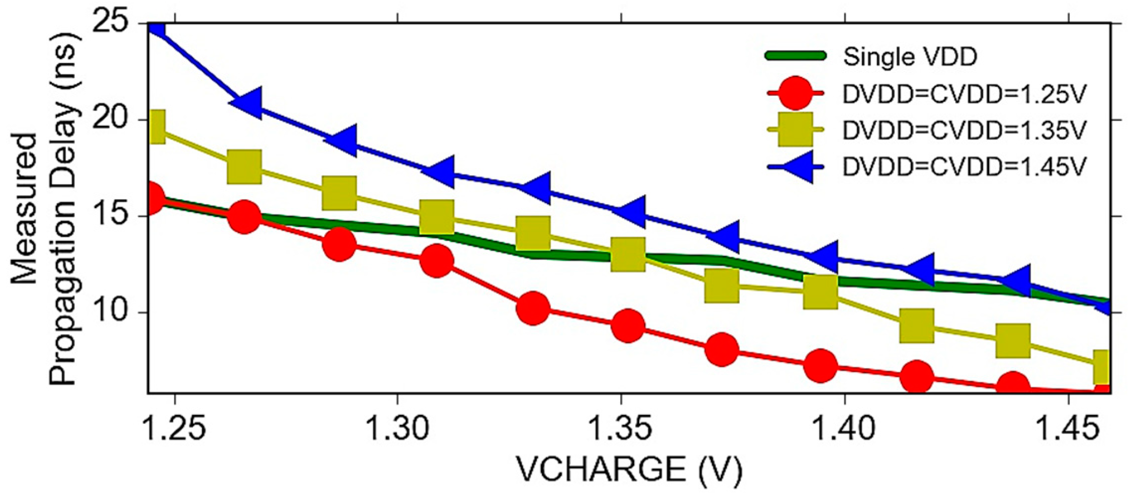
7. Experimental Results
8. Conclusions
Author Contributions
Funding
Conflicts of Interest
References
- Karam, R.; Puri, R.; Ghosh, S.; Bhunia, S. Emerging Trends in Design and Applications of Memory-Based Computing and Content-Addressable Memories. Proc. IEEE 2015, 103, 1311–1330. [Google Scholar] [CrossRef]
- Pagiamtzis, K.; Sheikholeslami, A. Content-Addressable Memory (CAM) Circuits and Architectures: A Tutorial and Survey. IEEE J. Solid-State Circuits 2006, 41, 712–727. [Google Scholar] [CrossRef] [Green Version]
- Hoff, J.R.; Deptuch, G.W.; Joshi, S.; Liu, T.; Olsen, J.; Shenai, A. VIPRAM_L1CMS: A 2-Tier 3D Architecture for Pattern Recognition for Track Finding. In Proceedings of the 2016 IEEE Nuclear Science Symposium, Medical Imaging Conference and Room-Temperature Semiconductor Detector Workshop (NSS/MIC/RTSD), Strasbourg, France, 29 October–6 November 2016; pp. 1–7. [Google Scholar]
- Tony, S.M.; Wu, F.; Li, H.; Huang, P.; Rahimi, A.; Rabaey, J.M.; Wong, H.-S.P.; Shulaker, M.M. Brain-Inspired Computing Exploiting Carbon Nanotube FETs and Resistive RAM: Hyperdimensional Computing Case Study. In Proceedings of the 2018 IEEE International Solid-State Circuits Conference, San Francisco, CA, USA, 11–15 February 2018; pp. 492–494. [Google Scholar]
- Li, H.; Wu, T.F.; Rahimi, A.; Li, K.-S.; Rusch, M.; Lin, C.-H.; Hsu, J.-L.; Sabry, M.M.; Eryilmaz, S.B.; Sohn, J.; et al. Hyperdimensional computing with 3D VRRAM in-memory kernels: Device-architecture co-design for energy-efficient, error-resilient language recognition. In Proceedings of the 2016 IEEE International Electron Devices Meeting (IEDM), San Francisco, CA, USA, 3–7 December 2016; pp. 16.1.1–16.1.4. [Google Scholar]
- Liu, T.; Hoff, J.; Deptuch, G.; Yarema, R. A New Concept of Vertically Integrated Pattern Recognition Associative Memory. Phys. Procedia 2012, 37, 1973–1982. [Google Scholar] [CrossRef]
- Hu, Y.J.; Li, J.F.; Huang, Y.J. 3-D content addressable memory architectures. In Proceedings of the 2009 IEEE International Workshop on Memory Technology, Design, and Testing, Hsinchu, Taiwan, 31 August–2 September 2009; pp. 59–64. [Google Scholar]
- Mathan, K.; Ravichandran, T. Data Intelligent Low Power High Performance TCAM for IP-Address Lookup Table. Circuits Syst. 2016, 7, 3734–3745. [Google Scholar] [CrossRef]
- Guo, Q.; Guo, X.; Bai, Y.; İpek, E. A Resistive TCAM Accelerator for Data-Intensive Computing Categories and Subject Descriptors. In Proceedings of the 2011 44th Annual IEEE/ACM International Symposium on Microarchitecture (MICRO), Porto Alegre, Brazil, 3–7 December 2011; pp. 339–350. [Google Scholar]
- Rahimi, A.; Ghofrani, A.; Cheng, K.; Benini, L.; Gupta, R.K. Approximate Associative Memristive Memory for Energy-Efficient GPUs. In Proceedings of the 2015 Design, Automation & Test in Europe Conference & Exhibition (DATE), Grenoble, France, 9–13 March 2015; pp. 1497–1502. [Google Scholar]
- Ghofrani, A.; Rahimi, A.; Lastras-Montano, M.A.; Benini, L.; Gupta, R.K.; Cheng, K.T. Associative Memristive Memory for Approximate Computing in GPUs. IEEE J. Emerg. Sel. Top. Circuits Syst. 2016, 6, 222–234. [Google Scholar] [CrossRef]
- Imani, M.; Rahimi, A.; Rosing, T.S. Resistive Configurable Associative Memory for Approximate Computing. In Proceedings of the 2016 Design, Automation & Test in Europe Conference & Exhibition (DATE), Dresden, Germany, 14–18 March 2016; pp. 1327–1332. [Google Scholar]
- Wade, J.P.; Sodini, C.G. A Ternary Content Addressable Search Engine. IEEE J. Solid-State Circuits 1989, 24, 1003–1013. [Google Scholar] [CrossRef]
- Deptuch, G.; Hoff, J.; Jndariani, S.; Liu, T.; Olsen, J.; Tran, N.; Joshi, S.; Li, D.; Ogrenci-Memik, S. Performance Study of the First 2D Prototype of Vertically Integrated Pattern Recognition Associative Memory (VIPRAM). arXiv, 2017; arXiv:1709.08303. [Google Scholar]
- Liu, T.; Deptuch, G.; Hoff, J.; Jndariani, S.; Joshi, S.; Olsen, J.; Tran, N.; Trimpl, M. Design and testing of the first 2D Prototype Vertically Integrated Pattern Recognition Associative Memory. J. Instrum. 2015, 10, 1–8. [Google Scholar] [CrossRef]
- Annovi, A.; Bertolucci, F.; Biesuz, N.; Calabro, D.; Calderini, G.; Citraro, S.; Crescioli, F.; Dimas, D.; Dell’Orso, M.; Donati, S.; et al. Highly parallelized pattern matching execution for the ATLAS experiment. In Proceedings of the 2015 IEEE Nuclear Science Symposium and Medical Imaging Conference (NSS/MIC), San Diego, CA, USA, 31 October–7 November 2015; pp. 15–17. [Google Scholar]
- CMS Collaboration. Technical Proposal for the Phase-II Upgrade of the CMS Detector. CERN-LHCC-2015-010, LHCC-P-008. 2015. Available online: https://cds.cern.ch/record/2020886 (accessed on 28 July 2018).
- Annovi, A.; Beretta, M.M.; Calderini, G.; Crescioli, F.; Frontini, L.; Liberali, V.; Shojaii, S.R.; Stabile, A. AM06: The Associative Memory chip for the Fast TracKer in the upgraded ATLAS detector. J. Instrum. 2017, 12. [Google Scholar] [CrossRef]
- Lehtonen, E.; Poikonen, J.H.; Laiho, M.; Kanerva, P. Large-scale memristive associative memories. IEEE Trans. Very Large Scale Integr. Syst. 2014, 22, 562–574. [Google Scholar] [CrossRef]
- Joshi, S.; Li, D.; Ogrenci-Memik, S.; Deptuch, G.; Hoff, J.; Jindariani, S.; Liu, T.; Olsen, J.; Tran, N. A Content Addressable Memory with Multi-Vdd Scheme for Low Power Pattern Recognition. In Proceedings of the 60th IEEE International Midwest Symposium on Circuits and Systems, Boston, MA, USA, 6–9 August 2017. [Google Scholar]
- Zackriya, M.; Kittur, H.M. Content Addressable Memory—Early predict and terminate precharge of Match-Line Content Addressable Memory. IEEE Trans. Very Large Scale Integr. Syst. 2016, 25, 385–387. [Google Scholar] [CrossRef]
- Pagiamtzis, K.; Sheikholeslami, A. A low-power content-addressable memory (CAM) using pipelined hierarchical search scheme. IEEE J. Solid-State Circuits 2004, 39, 1512–1519. [Google Scholar] [CrossRef] [Green Version]
- Mahendra, T.V.; Mishra, S.; Dandapat, A. Self-Controlled High-Performance Precharge-Free Content-Addressable Memory. IEEE Trans. Very Large Scale Integr. Syst. 2017, 25, 2388–2392. [Google Scholar] [CrossRef]
- Mohan, N.; Sachdev, M. Low-Leakage Storage Cells for Ternary Content. IEEE Trans. Very Large Scale Integr. Syst. 2009, 17, 604–612. [Google Scholar] [CrossRef]
- Arsovski, I.; Chandler, T.; Sheikholeslami, A. A ternary content-addressable memory (TCAM) based on 4T static storage and including a current-race sensing scheme. IEEE J. Solid-State Circuits 2003, 38, 155–158. [Google Scholar]
- Zukowski, C.; Wang, S.-Y. Use of selective precharge for low-power content-addressable memories. In Proceedings of the 1997 IEEE International Symposium on Circuits and Systems. Circuits and Systems in the Information Age ISCAS’97, Hong Kong, China, 12 June 1997; pp. 1788–1791. [Google Scholar]
- Do, A.; Yin, C.; Velayudhan, K.; Lee, Z.; Yeo, K.; Kim, T. 0.77 fJ/bit/search Content Addressable Memory Using Small Match Line Swing and Automated Background Checking Scheme for Variation Tolerance. IEEE J. Solid-State Circuits 2014, 49, 1487–1498. [Google Scholar] [CrossRef]
- Mohan, N.; Sachdev, M. A Static Power Reduction Technique for Ternary Content Addressable Memories. In Proceedings of the Canadian Conference on Electrical and Computer Engineering 2004, Niagara Falls, ON, Canada, 2–5 May 2004; pp. 711–714. [Google Scholar]
- Agarwal, A.; Hsu, S.K.; Kaul, H.; Anders, M.A.; Krishnamurthy, R.K. A Dual-Supply GHz 13 fJ/bit/search 64 × 128b CAM in 65 nm CMOS. In Proceedings of the 2006 32nd European Solid-State Circuits Conference, Montreux, Switzerland, 19–21 September 2006; pp. 4–7. [Google Scholar]
- Mohan, N.; Sachdev, M. Low-capacitance and charge-shared match lines for low-energy high-performance TCAMs. IEEE J. Solid-State Circuits 2007, 42, 2054–2060. [Google Scholar] [CrossRef]
- Yang, B.D.; Lee, Y.K.; Sung, S.W.; Min, J.J.; Oh, J.M.; Kang, H.J. A low power content addressable memory using low swing search lines. IEEE Trans. Circuits Syst. I Regul. Pap. 2011, 58, 2849–2858. [Google Scholar] [CrossRef]
- Arsovski, I.; Sheikholeslami, A. A mismatch-dependent power allocation technique for match-line sensing in content-addressable memories. IEEE J. Solid-State Circuits 2003, 38, 1958–1966. [Google Scholar] [CrossRef]
- Igarashi, M.; Usami, K.; Nogami, K.; Minami, F.; Kawasaki, Y.; Aoki, T.; Takano, M.; Sonoda, S.; Ichida, M.; Hatanaka, N. A low-power design method using multiple supply voltages. In Proceedings of the 1997 International Symposium on Low Power Electronics and Design, Monterey, CA, USA, 18–20 August 1997; pp. 36–41. [Google Scholar]
- Usami, K.; Horowitz, M. Clustered voltage scaling technique for low-power design. In Proceedings of the 1995 International Symposium on Low Power Design, Dana Point, CA, USA, 23–26 April 1995; pp. 3–8. [Google Scholar]
- Mondal, H.K.; Gade, S.H.; Kishore, R.; Deb, S. Adaptive Multi-Voltage Scaling in Wireless NoC for High Performance Low Power Applications. In Proceedings of the 2016 Design, Automation & Test in Europe Conference & Exhibition (DATE), Dresden, Germany, 14–18 March 2016; pp. 1315–1320. [Google Scholar]
- Friedman, E.G.; Kursun, V. Multi-Voltage CMOS Circuit Design; John Wiley & Sons: Hoboken, NJ, USA, 2006. [Google Scholar]
- Shibata, N.; Watanabe, M.; Okiyama, H. A high-speed low-power multi-VDD CMOS/SIMOX SRAM with LV-TTL level input/output pins-write/read assist techniques for 1-V operated memory cells. IEEE J. Solid-State Circuits 2010, 45, 1856–1869. [Google Scholar] [CrossRef]
- Kulkarni, J.; Khellah, M.; Tschanz, J.; Geuskens, B.; Jain, R.; Kim, S.; De, V. Dual-VCC 8T-bitcell SRAM Array in 22 nm tri-gate CMOS for energy-efficient operation across wide dynamic voltage range. In Proceedings of the 2013 Symposium on VLSI Circuits, Kyoto, Japan, 12–14 June 2013; pp. 352–353. [Google Scholar]
- Koo, K.-H.; Wei, L.; Keane, J.; Bhattacharya, U.; Karl, E.A.; Zhang, K. A 0.094 um2 High Density and Aging Resilient 8T SRAM with 14 nm FinFET Technology Featuring 560 mV VMIN with Read and Write Assist. In Proceedings of the 2015 Symposium on VLSI, Kyoto, Japan, 17–19 June 2015. [Google Scholar]
- Takeda, K.; Hagihara, Y.; Aimoto, Y.; Nomura, M.; Nakazawa, Y.; Ishii, T.; Kobatake, H. A Read-Static-Noise-Margin-Free SRAM Cell for low-VDD high speed applications. IEEE J. Solid-State Circuits 2006, 41, 113–121. [Google Scholar] [CrossRef]
- Mondal, S.; Memik, S.O. A low power FPGA routing architecture. In Proceedings of the 2005 IEEE International Symposium on Circuits and Systems, Kobe, Japan, 23–26 May 2005; pp. 1222–1225. [Google Scholar]
- Mukherjee, R.; Memik, S. Evaluation of dual VDD fabrics for low power FPGAs. In Proceedings of the 2005 Design Automation Conference, Anaheim, CA, USA, 13–17 June 2005; pp. 1240–1243. [Google Scholar]
- Mukherjee, R.; Liu, S.; Merik, S.O.; Mondal, S. A high-level clustering algorithm targeting dual Vdd FPGAs. ACM Trans. Des. Autom. Electron. Syst. 2008, 13, 57. [Google Scholar] [CrossRef]
- Li, F.; Lin, Y.; He, L. FPGA power reduction using configurable dual-vdd. In Proceedings of the 2004 Design Automation Conference, San Diego, CA, USA, 7–11 June 2004. [Google Scholar]
- Mondal, S.; Memik, S.O. Power optimization techniques for SRAM-based FPGAS. In Proceedings of the 2006 International Conference on Field Programmable Logic and Applications, Madrid, Spain, 28–30 August 2006; pp. 959–960. [Google Scholar]
- Mukherjee, R.; Memik, S.O. Power-Driven Design Partitioning. In Proceedings of the International Conference on Field Programmable Logic and Applications, Leuven, Belgium, 30 August–1 September 2004. [Google Scholar]
- Do, A.T.; Chen, S.; Kong, Z.H.; Yeo, K.S. A low-power CAM with efficient power and delay trade-off. In Proceedings of the 2011 IEEE International Symposium of Circuits and Systems (ISCAS), Rio de Janeiro, Brazil, 15–18 May 2011; pp. 2573–2576. [Google Scholar]
- Augsburger, S.; Nikolić, B. Combining Dual-Supply, Dual-Threshold and Transistor Sizing for Power Reduction. In Proceedings of the IEEE International Conference on Computer Design: VLSI in Computers and Processors, Freiberg, Germany, 18 September 2002. [Google Scholar]
- Chandrakasan, A.P.; Sheng, S.; Brodersen, R.W. Low-power CMOS digital design. IEEE J. Solid-State Circuits 1992, 27, 473–484. [Google Scholar] [CrossRef] [Green Version]
- Gonzalez, R.; Gordon, B.M.; Horowitz, M.A. Supply and Threshold Voltage Scaling for Low Power CMOS. IEEE J. Solid-State Circuits 1997, 32, 1210–1216. [Google Scholar] [CrossRef]
- Bijansky, S.; Lee, S.K. TuneLogic: Post-Silicon Tuning of Dual-Vdd Designs. In Proceedings of the 2009 10th International Symposium on Quality Electronic Design, San Jose, CA, USA, 16–18 March 2009. [Google Scholar]
- Usami, K.; Igarashi, M. Low-power design methodology and applications utilizing dual supply voltages. In Proceedings of the Design Automation Conference, Yokohama, Japan, 25–28 January 2000; pp. 123–128. [Google Scholar]
- Li, D.; Joshi, S.; Ogrenci-Memik, S.; Hoff, J.; Jindariani, S.; Liu, T.; Olsen, J.; Tran, N. A methodology for power characterization of associative memories. In Proceedings of the 2015 33rd IEEE International Conference on Computer Design (ICCD), New York, NY, USA, 18–21 October 2015; pp. 491–498. [Google Scholar]
- Qin, H.; Cao, Y.; Markovic, D.; Vladimirescu, A.; Rabaey, J. SRAM leakage suppression by minimizing standby supply voltage. In Proceedings of the 2003 International Symposium on Signals, Circuits and Systems, San Jose, CA, USA, 22–24 March 2004; pp. 2–7. [Google Scholar]
- Frazier, R.; Iles, G.; Newbold, D.; Rose, A. Software and firmware for controlling CMS trigger and readout hardware via gigabit Ethernet. Phys. Procedia 2012, 37, 1892–1899. [Google Scholar] [CrossRef]


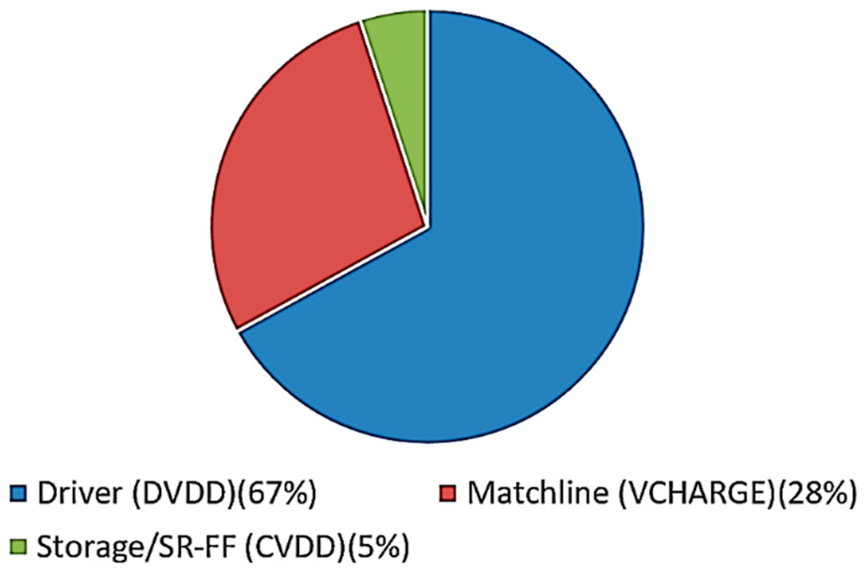
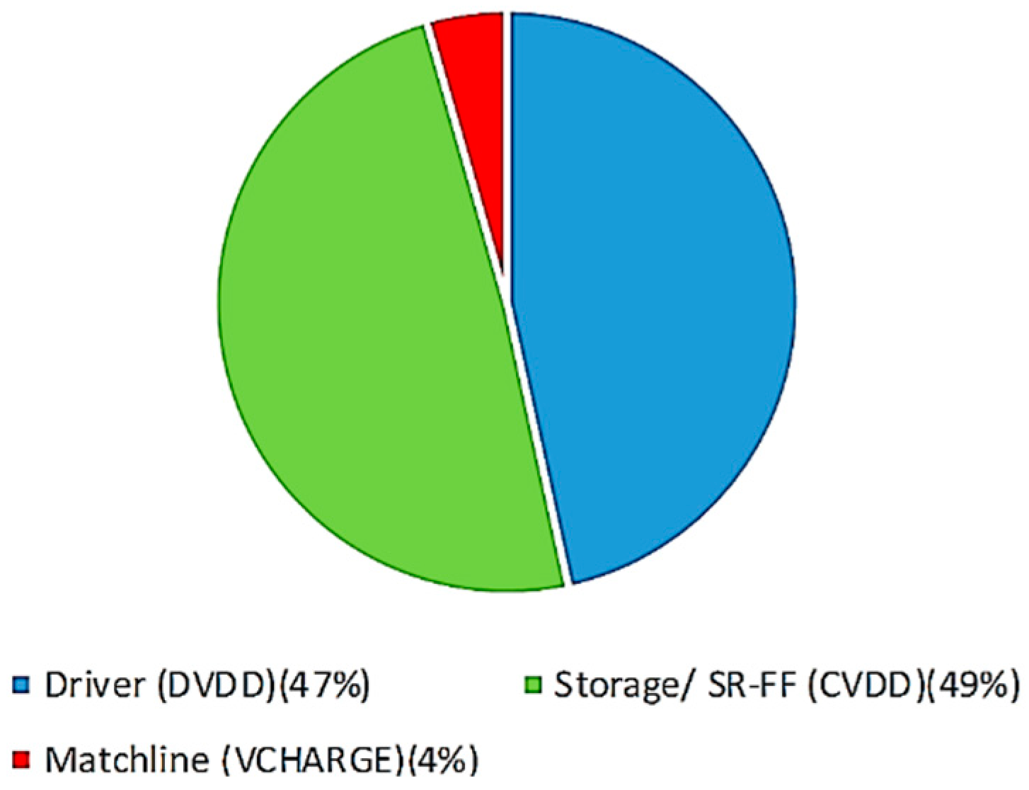
| Supply | Components Supplied |
|---|---|
| VCHARGE | Matchline |
| CVDD | SRAM, sense-amplifier (SR-FF) |
| DVDD (Driver-Vdd) | Data (Senseline) and Clock (CLK) Drivers |
© 2018 by the authors. Licensee MDPI, Basel, Switzerland. This article is an open access article distributed under the terms and conditions of the Creative Commons Attribution (CC BY) license (http://creativecommons.org/licenses/by/4.0/).
Share and Cite
Joshi, S.; Li, D.; Ogrenci-Memik, S.; Deptuch, G.; Hoff, J.; Jindariani, S.; Liu, T.; Olsen, J.; Tran, N. Multi-Vdd Design for Content Addressable Memories (CAM): A Power-Delay Optimization Analysis. J. Low Power Electron. Appl. 2018, 8, 25. https://doi.org/10.3390/jlpea8030025
Joshi S, Li D, Ogrenci-Memik S, Deptuch G, Hoff J, Jindariani S, Liu T, Olsen J, Tran N. Multi-Vdd Design for Content Addressable Memories (CAM): A Power-Delay Optimization Analysis. Journal of Low Power Electronics and Applications. 2018; 8(3):25. https://doi.org/10.3390/jlpea8030025
Chicago/Turabian StyleJoshi, Siddhartha, Dawei Li, Seda Ogrenci-Memik, Grzegorz Deptuch, James Hoff, Sergo Jindariani, Tiehui Liu, Jamieson Olsen, and Nhan Tran. 2018. "Multi-Vdd Design for Content Addressable Memories (CAM): A Power-Delay Optimization Analysis" Journal of Low Power Electronics and Applications 8, no. 3: 25. https://doi.org/10.3390/jlpea8030025