Opportunistic Design Margining for Area and Power Efficient Processor Pipelines in Real Time Applications

1
VIRTUS, IC Design Centre of Excellence, School of Electrical and Electronic Engineering, Nanyang Technological University, Singapore 639798, Singapore
2
NXP Semiconductors Singapore Pte Ltd., 1 Fusionopolis Walk, #12-01/02 South Tower, Solaris, Singapore 138628, Singapore
*
Author to whom correspondence should be addressed.
J. Low Power Electron. Appl. 2018, 8(2), 9; https://doi.org/10.3390/jlpea8020009
Submission received: 9 February 2018
/
Revised: 13 March 2018
/
Accepted: 18 March 2018
/
Published: 21 March 2018
Abstract
:The semiconductor industry is strategically focusing on automotive markets, and significant investment is targeted to addressing these markets. Runtime better-than-worst-case designs like Razor lead to massive timing errors upon breaching the critical operating point and have significant area overheads. As we scale to higher-reliability automotive and industrial markets we need alternative techniques that will allow full extraction of the power benefits without sacrificing reliability. The proposed method utilizes positive slack available in the pipeline stages and re-distributes it to the preceding critical logic stage using Slack Balancing Flip-Flops (SBFFs). We use opportunistic under designing to get rid of the area, power and error correction overheads associated with the speculative hardware of runtime techniques. The proposed logic reshaping results in 12 percent and eight percent power and area savings respectively compared to the worst-case design approach. Compared to runtime better-than-worst-case designs, we get 51 percent and 10 percent power and area savings, respectively. In addition, the timing budgeting and timing correction using opportunistic slack eliminate critical operating point behavior, metastability issues and hold buffer overheads encountered in existing runtime resilience techniques.
1. Introduction
Technology scaling has benefited integrated circuits by meeting their power, performance and area goals over generations. However, it has also aggravated circuits and system failures creating major cost and reliability impacts in nanoscale designs [1,2]. Advanced technology nodes show a significant amount of intra-die variations due to process inaccuracies [3,4,5]. Dynamic variations caused by voltage and temperature fluctuations also cause reliability issues [6]. These reliability issues shrink the design life cycle. The impacts of variations continue to increase with process technology scaling, which leads to pessimistic delay margins in processor pipelines. This stretches the timing guard bands in traditional designs. The worst-case design margins result in overdesign and wastage of chip resources. Therefore, we need opportunistic design techniques to improve the chip yield without compromising performance and energy efficiency, which are highly demanded.
Digital circuits do not always face the worst operating conditions. Several alternative techniques have been proposed to dynamically tune the operating conditions in real time to recover the design margins. Sensor-based adaptive techniques help to combat static and dynamic variations [7,8]. Hardware signatures from sensors are used to tune the circuit operating point [9,10]. However, sensors may not respond fast enough to dynamic variations. In addition, sensors need to be calibrated to determine safe operation regions through post-silicon tuning. Another technique is to use critical path replicas to monitor variations [11]. However, they fail to detect the actual amount of variation due to the mismatch between the actual path and the replica path.
In situ error correction techniques illustrated in Figure 1 help to overcome the drawbacks of the sensor-based designs. They tune supply voltage to the point of failure to minimize design margins and reclaim power. Timing errors due to dynamic variations are then detected and corrected using special flip-flops. However, the dynamic tuning of the operating point makes the in situ schemes vulnerable to metastability issues in data paths and/or error paths, which affects the overall system recovery. Razor I [12] illustrated in Figure 1a has a metastability issue in the data path since data are allowed to change very close to the clock (CLK) edge. Razor II [13] in Figure 1b overcomes the metastability in the data path using a latch. Double Sampling with Time Borrowing (DSTB) [14] and Transition Detection with Time Borrowing (TDTB) [14] are similar to Razor II, employing a latch as the data path. However, the delayed sampling leads to short path violations and buffer overheads. Bubble Razor [15] uses two-phase latch timing to overcome the short path violations. However, there is a performance penalty for error recovery during heavy workloads.
Runtime techniques come with high-cost overheads, latency issues and the risk of runtime error handling. In the Razor approach, the voltage adaptation is based on the measured timing error rate. As errors have to be accepted, architectural recovery circuits are necessary, which increases design time and cost. Besides the undesirable increase in complexity, error recovery also leads to variable and unpredictable latency, which causes catastrophic failures. Error masking techniques in Figure 1c like soft edge flip-flops [16] and Time Borrowing and Error Relay (TIMBER [17]) mask timing errors by borrowing time from the subsequent pipeline stages with zero latency overheads. However, they have limited design margin reduction and metastability and hold buffer overheads. Runtime techniques reclaim power, area and performance by using dynamic/adaptive voltage/frequency scaling and Better-than-Worst-Case (BTWC) design techniques [18,19,20].
Design margins are also recovered by redistributing slack to the critical pipeline stages using combinatorial and sequential optimizations. Sequential optimizations like retiming help to minimize clock period, achieve low power and maximize tolerance to variations [21,22]. However, it restricts the space of possible retiming and may result in unnecessary area overheads. Useful skew and clock skew scheduling [23] combined with gate sizing [24,25] help to compensate variations and speed up the processor pipelines. EVAL (Environment for Variation-Afflicted Logic) speeds up the timing of critical paths through Adaptive Body Bias (ABB), as well as Adaptive Supply Voltage (ASV) [26], but it has significant area overheads. Blue Shift uses On-demand Selective Biasing (OSB) and Path Constrained Tuning (PCT) [27] to achieve performance gains at the cost of significant power overheads. Such design optimizations worsen the critical operating point of the design [28], which limits the effectiveness of the voltage scaling. Power-aware slack distribution (SlackOptimizer) [29] uses cell sizing together with Razor voltage scaling to distribute slack evenly in a power- and cost-efficient manner. However, they retain metastability and hold buffer overheads of the speculative pipelines. Pulsed latches [30,31] are used as a means to reduce power consumption, but just like other latch-based systems, it is difficult to verify the design timing. Moreover, pulse width integrity issues and pulse generation overheads need to be taken care of while using such systems. The latency issues inherent in run time techniques makes them unsuitable for real-time applications [32,33]. For higher-reliability automotive markets, we need alternative techniques that will allow full extraction of the power benefits without sacrificing reliability [34].
Techniques that trade off critical path slack with non-critical slack such as path constraint tuning [27] and SlackOptimizer [29] over constrain the critical logic and reclaim the power by under constraining the non-critical logic. Our methodology is different in the fact that we under-design the critical logic and thereby get more power and area reductions from the usual over constrained counterparts. Compared to the existing speculative slack exploitation techniques like soft edge flip-flops [16] and TIMBER, we use available slack in the design, thereby achieving PPA reductions independent of timing error rates. The reclaimed slack for the proposed method remains constant independent of the error rate, as shown in Figure 2. Moreover, the existing optimizations based on retiming [22], skew scheduling [23] and gate sizing [25] do not fully reclaim the available slack to be traded off with power/performance. They also limit the amount of time borrowed due to hold violations. The proposed approach has significant slack gain compared to the existing techniques, as shown in Figure 2. Our paper uses a design-time method, which uses a speculative hardware similar to the runtime methods to allow better-than-worst-case operation. We use opportunistic under designing to get rid of the area, power and error correction overheads associated with the speculative hardware of runtime techniques. Runtime techniques show significant area overhead [33]. Table 1 compares the different cost-effective resilient design techniques, which shows that only the proposed technique has zero area overhead.
Our paper relies on opportunistic better-than-worst-case design, which differs significantly from traditional worst-case design and at the same time gives area and power savings. We use worst-case design margins with respect to the delayed clock edge as shown in Figure 3, which categorically makes it a better-than-worst-case technique. We take advantage of the opportunistic slack and translate it into better-than-worst-case design margins while still achieving variation tolerance. Opportunistic logic downsizing helps to reclaim power at design time rather than scaling voltage at runtime. Therefore, we use the term “Opportunistic Better-Than-Worst-Case design” (OBTWC) to differentiate it from traditional Worst-Case Design (WCD) and runtime Better-Than-Worst-Case (BTWC) techniques. The proposed solution works in a conservative manner that guarantees “always correct” computation and timing correctness of the circuit with respect to the delayed clock edge, even in the worst-case scenario.
The proposed approach, which is an extension of our previous work [35], leverages the underutilized slack present in processor pipelines after the tool-based optimizations. We use Static Timing Analysis (STA) to look for near critical endpoints with sufficient consecutive slack after placement and logic optimizations. The critical endpoints are then back annotated to the synthesis tool, and we relax the timing margins of all the paths in the critical stage proportionate to the available slack. After relaxing the path slacks, we resynthesize the critical fan-in logic and replace the endpoints with Slack Balancing Flip-Flops (SBFF). SBFFs are designed to sample data at a delayed clock edge. Re-synthesis with relaxed timing margins delays the long paths and pushes them towards the SBFF delayed clock edge. The delayed data still maintain safe design margins with respect to the delayed clock edge of the SBFF. This removes metastability issues prevalent in the speculative flip-flop pipelines. The methodology relies on the critical wall of slack issues from the data path. Unlike the in-situ techniques, the short paths converging to the SBFF also get delayed, which removes the hold buffer overheads resulting from delayed data sampling. Re-synthesis downsizes and restructures the logic gates in the critical fan-in stage, which gives significant power and area savings. This results in the optimal power-aware design of the processor pipeline from the ground up without the failure risks of runtime speculative operating point tuning. They are not limited by the gate sizing and skew optimization constraints in typical combinatorial optimizations, which results in the maximum slack power trade-off along the processor pipeline. The remainder of this paper is organized as follows. Section 2 presents the motivation to use the proposed technique. Section 3 presents the proposed design methodology. Section 4 describes our proposed power optimization techniques, and experimental results are illustrated in Section 5. Finally, Section 6 concludes the proposed work.
2. Motivation
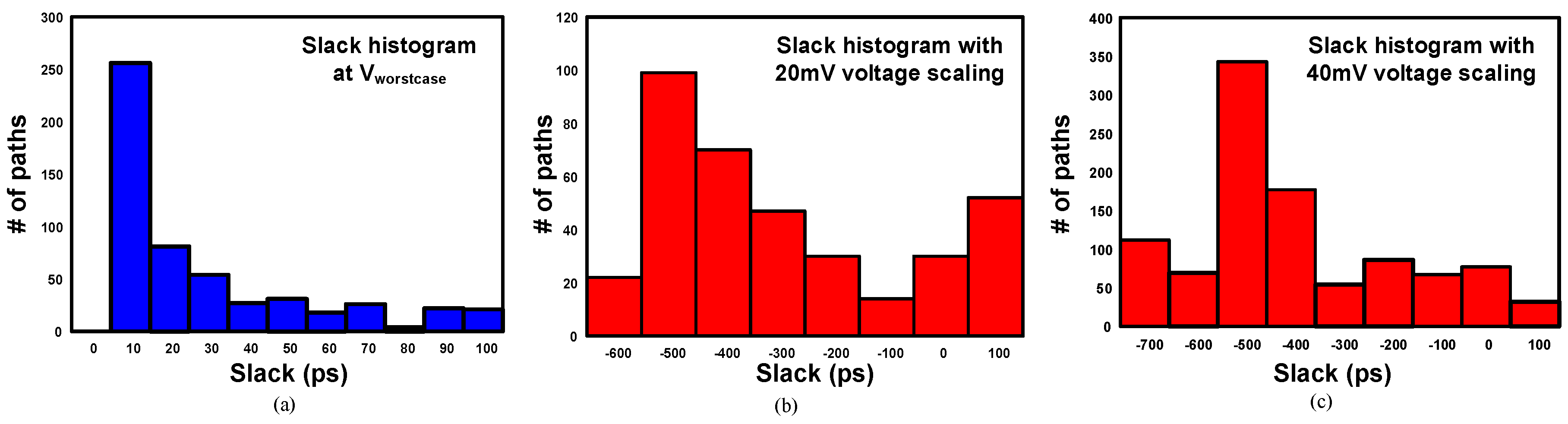
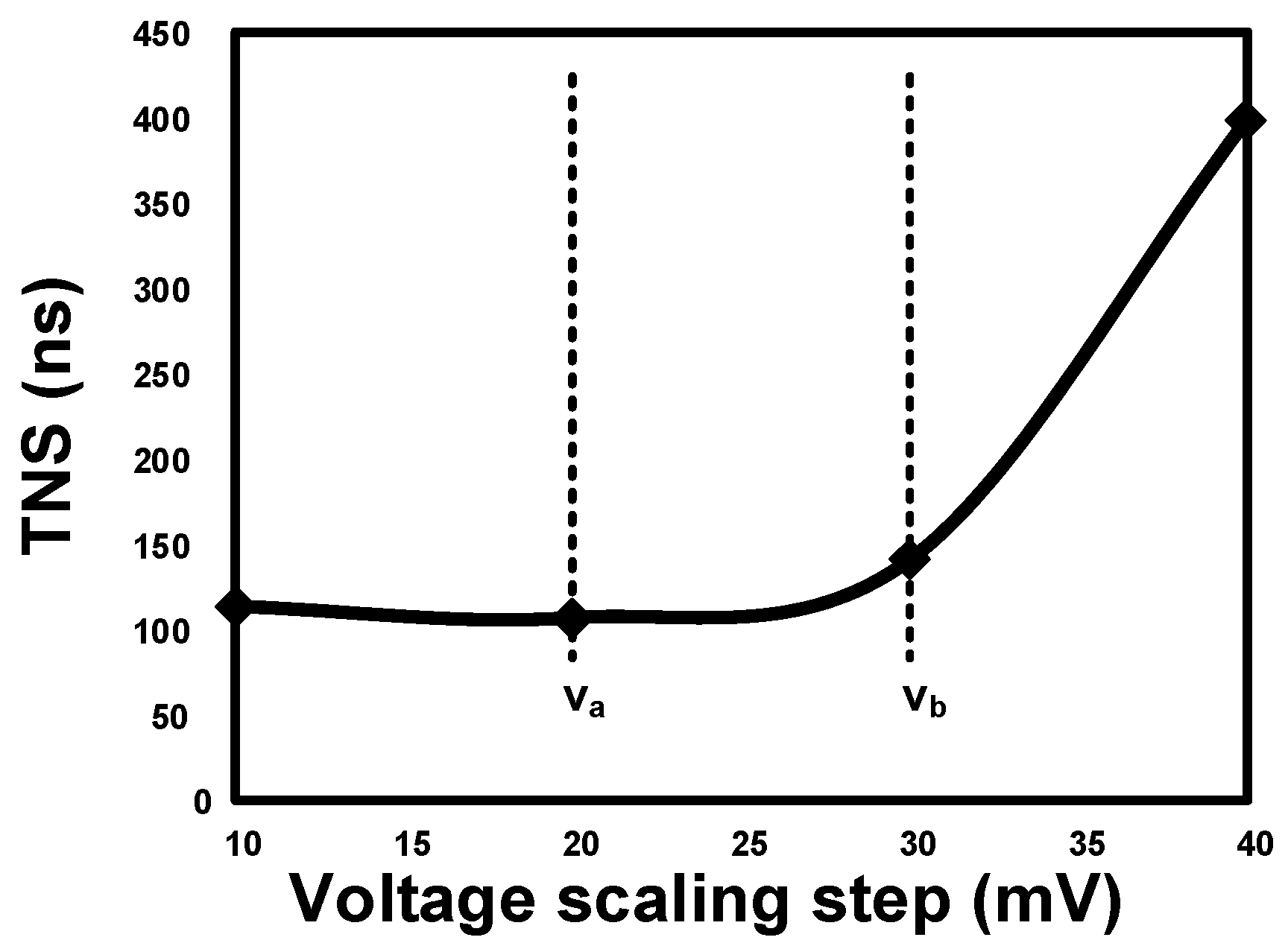
Conventional design margining approaches are based on dynamic operating point tuning and in situ error correction to trade off power and reliability. The operating conditions are tuned adaptively till Point of First Failure (PoFF), which makes the near critical paths also timing critical. Figure 3 shows the effect of voltage scaling on the slack histogram of critical paths in a processor pipeline. Figure 4a shows the baseline designed for the worst case with a Worst Negative Slack (WNS) of 10 ps. However, with the voltage scaling of 20 mV, 312 paths have negative slack, and the WNS becomes −600 ps (Figure 4b). Similarly, 985 paths have negative slack and the WNS becomes −700 ps when the supply voltage is scaled by 40 mV (Figure 4c). It is obvious that the paths with negative slack and the WNS increases with voltage scaling. The newly-created critical paths also need to be error resilient, which creates huge overheads in designs. Figure 5 plots the Total Negative Slack (TNS) of the processor pipeline against the voltage scaling steps. Voltage scaling down to Va does not increase TNS. TNS slightly increases between Va and Vb, but can be managed using in situ error correction techniques. Beyond Vb, TNS increases rapidly, and the increased number of critical paths makes the error correction cost enormous. In the event of high error rates, the system frequency has to be halved to recover from errors.
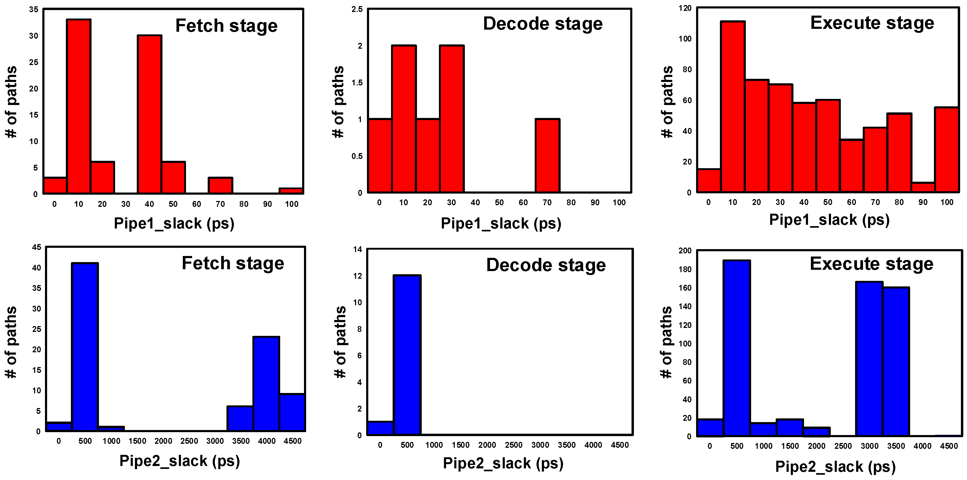
Traditional timing-driven optimizations focus on the combinational logic and do not support any tradeoffs between the logic paths separated by sequential elements. This results in a slack imbalance in the pipeline stages. Based on our timing analysis of a delay-optimized processor pipeline, we found that there is significant slack rebalance opportunity between the critical pipe_1 paths and the consecutive pipe_2 paths, as shown in Figure 6. We leverage this slack to relax and resynthesize the critical fan-in logic and sample the resulting delayed inputs using a slack balancing flip-flop. Instead of reducing design margins at runtime using adaptive techniques, the proposed approach downsizes the critical fan-in logic of the pipeline for power savings. Worst-case design margins are still met with respect to the delayed clock edge of the slack balancing flip-flop, which helps to eliminate metastability issue faced by adaptive in situ error correction schemes. Moreover, we also relax the short paths by the same design margin, which eliminates the need for SBFF-induced short path buffer insertions later in the design flow. In contrast to the existing slack redistribution techniques [21,22,23,24,25,26,27], we insert intentional clock delays to fully balance the available slack at the critical endpoints and redesign the whole critical logic stage with the relaxed time constraints. This results in a pipeline optimized for low power without the need for runtime voltage speculation, which is vulnerable to critical operating point behavior. The proposed method designs the processor to handle worst-case PVT margins. Logic downsizing pushes the critical data towards the delayed clock edge, which is timed to maintain worst-case margins with respect to the delayed clock edge. This makes the design resistant to static and dynamic variations similar to traditional worst-case corner designs, but with lower power and area. Razor and TIMBER depend on runtime voltage and frequency scaling to reclaim the design margins associated with dynamic variations. Therefore, they require error handling circuitry and need to tune the voltage or frequency back to the worst case operating corner depending on the error rate. There is a significant risk and architectural latency involved in this runtime adaption, especially when the error rate is high.
3. Proposed Variation Tolerant Pipeline Design
3.1. Slack Balancing Principle
To explain slack balancing, we consider a small circuit as shown in Figure 7 with four registers. The timing graph shows nodes corresponding to the registers and edges corresponding to the combinational paths. The maximum delay for each combinational path is shown beside the edges. This circuit is optimized for a minimum feasible clock period T = 11. The combinational path (d, b) has a maximum delay of 11. In this critical path, time can be borrowed from the consecutive stage (b, d) whose delay is nine. We replace the flip-flop b by the SBFF with a clock delay equal to the slack present in the consecutive stage (b, d), which is two. Now, for the same clock period T = 11, we have an extra margin of two in the fan-in paths (a, b) and (d, b). The extra margin is used to relax and downsize the logic in the fan-in paths, making sure it does not create other timing violations. This procedure also delays the short paths along the critical fan-in logic, thus eliminating the need for additional buffers compared to other timing speculation techniques.
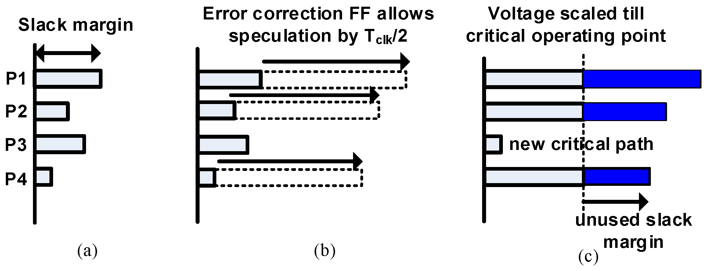
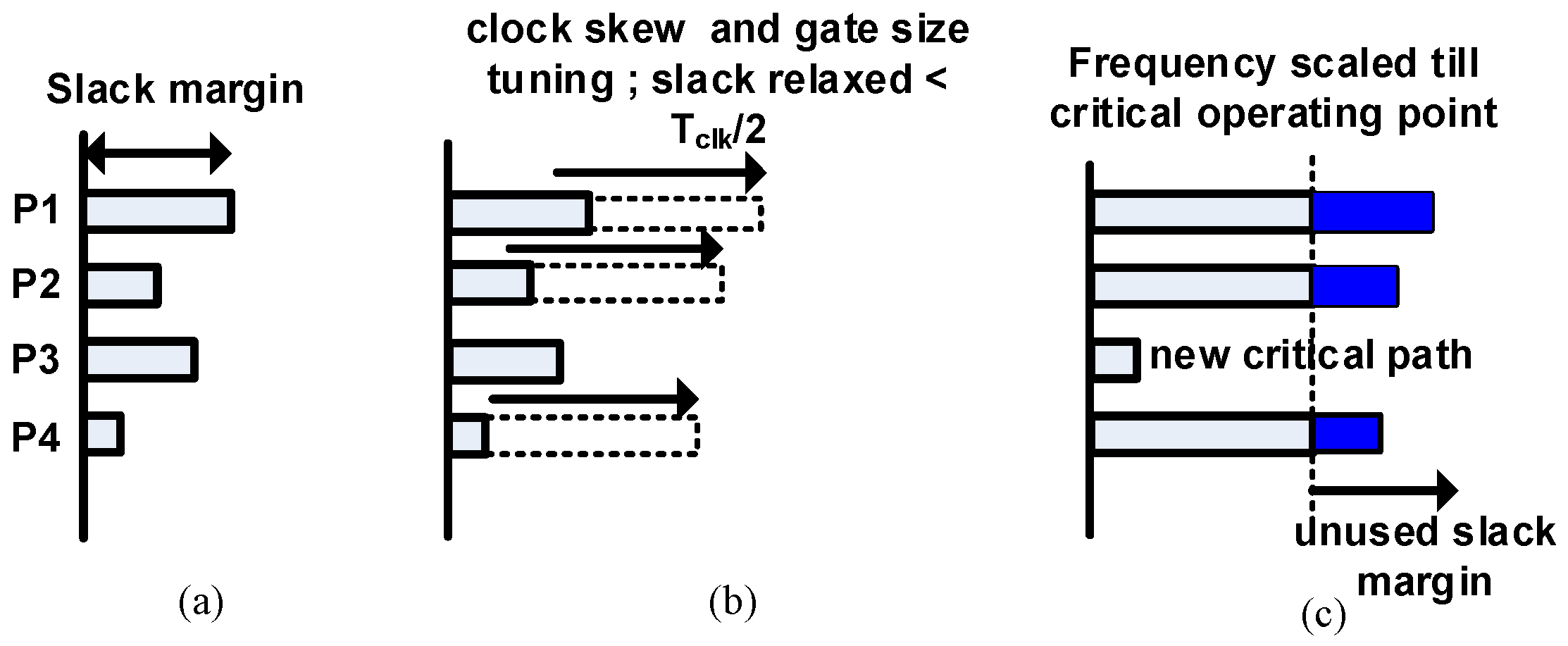
We compare the proposed technique with existing speculative error correction schemes. Figure 8a shows conceptually how the slack margins are relaxed in a typical voltage scaling-based error resilience scheme. We consider four timing paths P1, P2, P3 and P4 with different slack margins. Here, we assume P3 to be a part of a non-critical fan-in logic and P1, P2 and P4 in the critical fan-in logic with P1 being a critical short path. Energy can be reduced by scaling the supply voltage, which increases the delay along these paths. The timing speculation window for a typical speculative error resilience scheme is Tclk/2. Therefore, the paths are allowed to relax the delay margins by Tclk/2, as shown in Figure 8b. Voltage scaling is done beyond PoFF until the critical operating voltage near critical path P3 also becomes timing critical as depicted in Figure 8c. Moreover, runtime voltage scaling causes the inputs to change close to the clock edges, creating metastability issues. They also require additional buffers along P1 to ensure that it will not corrupt the delayed data and hence the error generated. Even if timing speculation is not done till Tclk/2, we still need to insert buffers for an equivalent delay of Tclk/2 to ensure that the error signal is not corrupted. Unless we use a fine-grain voltage scaling, even non-critical paths like P3 will become critical. Furthermore, for performance-driven design margin relaxation techniques, the slack relaxations are suboptimal as shown in Figure 9b. Frequency scaling results in new critical path formations in P3, as shown in Figure 9c, which makes the scaling bounded.
In our proposed technique, we use static time borrowing to trade off slack margin for power and area gains. Figure 10a shows the slack margins of the baseline worst-case design. We look for positive slack in the pipeline stages and replace the critical endpoints with SBFFs, which borrows a time TB proportional to the available slacks as depicted in Figure 10b. As a result, the critical fan-in paths P1, P2 and P4 are relaxed by TB. We re-synthesize the pipeline to downsize the fan-in logic of SBFF for power and area reductions (Figure 10c). After resizing the logic, timing closure is done on the data paths with respect to the delayed clock edges of SBFF. Our approach is deterministic and non-speculative, unlike the usual dynamic operating point scaling techniques. Safe design margins are kept with respect to the delayed clock edge of the SBFF, which prevents metastability issues in the pipeline. Unlike conventional resilience schemes, the short path P1 is also delayed by the corresponding TB window TB1. This eliminates the need for additional short path buffers along P1 to prevent it from corrupting the delayed data. Note that the time borrow window TB is fully utilized for power and area reduction compared to other optimization techniques. Unlike clock skew scheduling, which is mostly used for performance enhancements, the proposed method targets critical logic power minimization by utilizing maximum available slack to downsize all logic paths in the critical stage.
3.2. Slack Balancing Flip-Flop
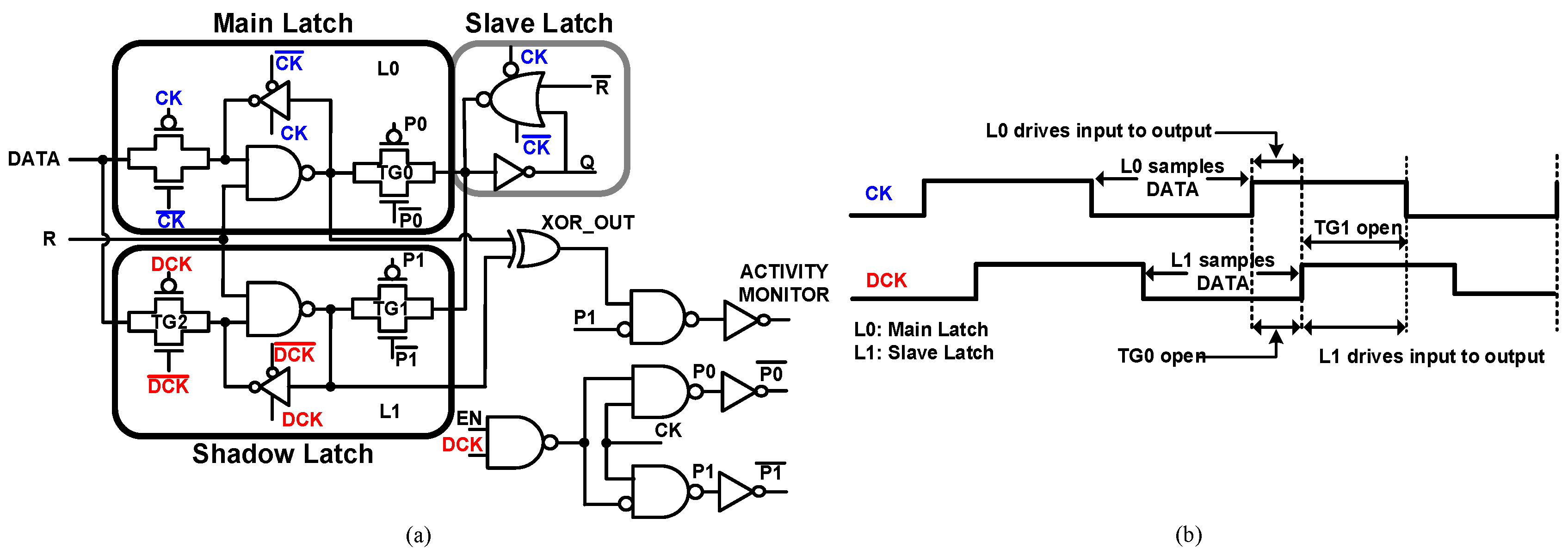
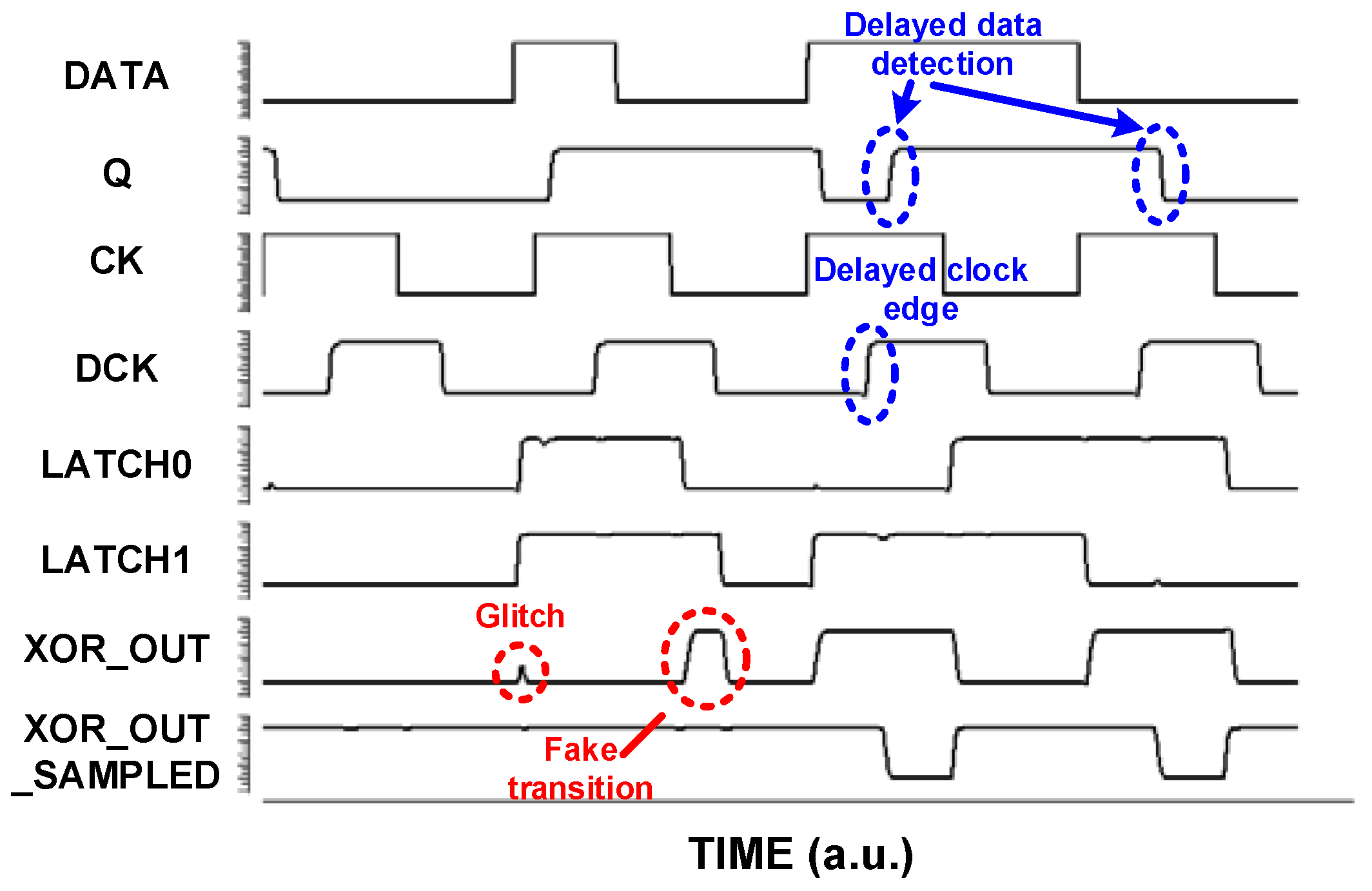
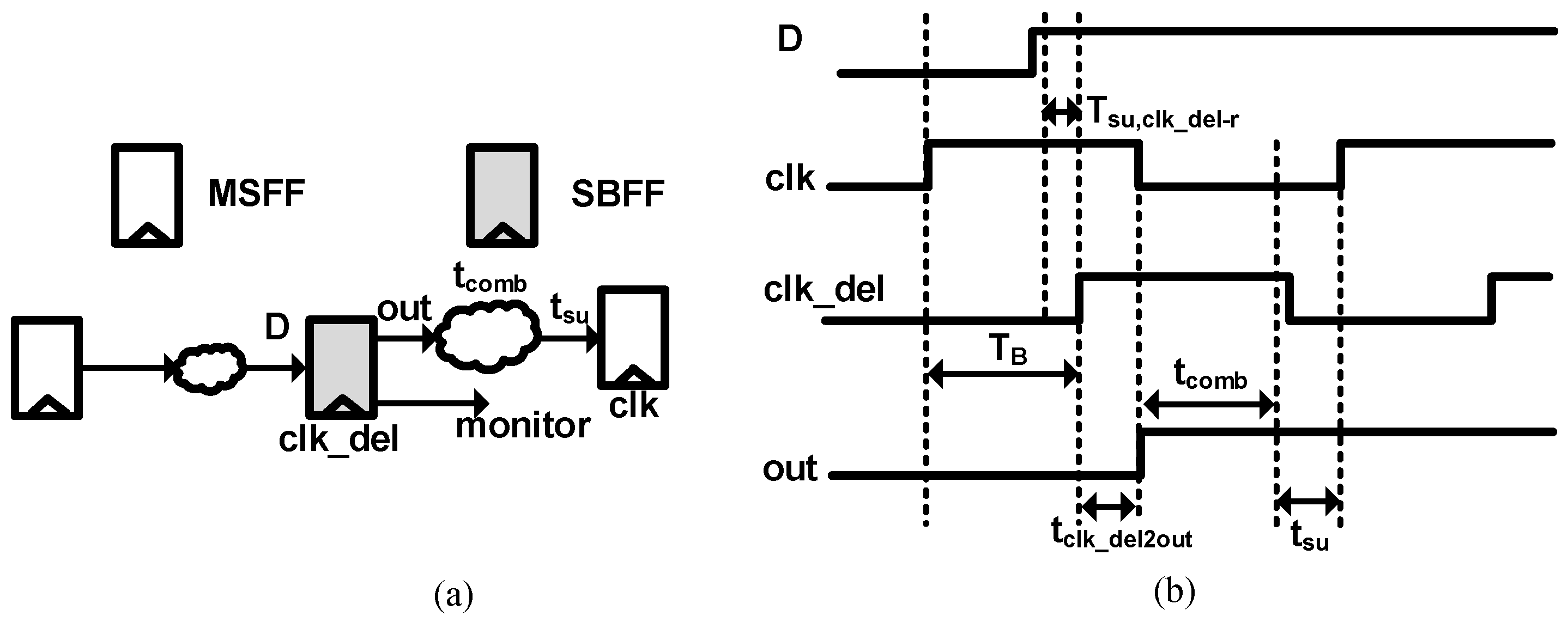
The SBFF and the timing diagram are illustrated in Figure 11. SBFF is a simplified version of TIMBER [17] without any error propagation logic. SBFF consists of the main latch, a shadow latch and a clock control circuit. The data path has a main latch and a slave latch forming an edge-triggered master-slave flip-flop. The proposed optimization technique downsizes the SBFF input logic for power reduction. This delays the input data signal DATA, which is detected by the shadow latch using a Delayed Clock (DCK). The delay amount decides the design margin improvement. The input to the slave latch is switched between the master path and the shadow path using the control signals (P0 and P1) to ensure that the delayed data pass through the slave latch. As shown in Figure 11, the main latch samples the input data and transfers them to the output (Q) at the positive Clock (CK) edge when TG0 is closed and TG1 is open. Similarly, the slave latch samples the data and passes them to the output at the Delayed Clock edge (DCK) when TG1 is closed and TG0 is open. The data in the master latch are compared with those in the slave latch by an XOR gate. The xor gate output signal XOR_OUT becomes ‘1’ when they are different. Figure 12 shows the simulation results of the SBFF. XOR_OUT is sampled by P1 to filter any glitches and fake transitions in the SBFF and generates a sampled signal XOR_OUT_SAMPLED. It shows that the delayed DATA are detected by the delayed clock DCK of the SBFF. The XOR output is also used to generate the monitor signal ACTIVITY MONITOR. Depending on whether a data transition happens in the clock cycle, the master latch and shadow latch will sample the same value or a different value. This will be handy in the pre-silicon or post-silicon stage to disable the time borrowing in the event of low data activity rates, which results in further power reduction. In Figure 13a, the monitor signal is triggered only once, which shows a low data rate. The monitor signal is triggered continuously in all the clock cycles as shown in Figure 13b for high data rates.
3.3. Pipeline Design Flow Using SBFF
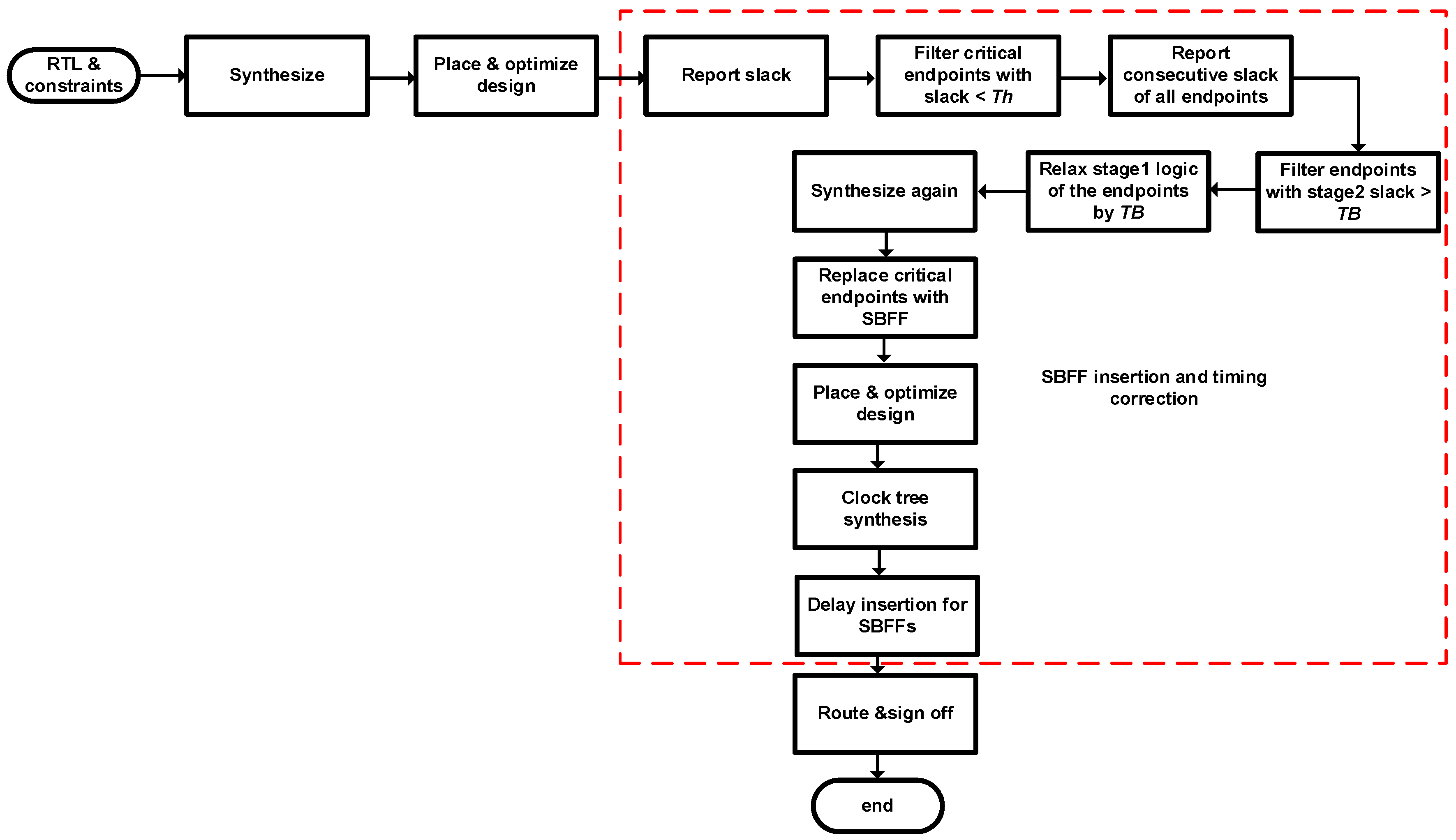
We use standard CAD tools and custom add-on scripts for SBFF insertion and logic optimization for the proposed pipeline design. A standard cell library with 20 different flavors of SBFFs was developed using library characterization tools to replace the normal flip-flops. The library has four sets of non-scan flip-flops with two different drive strengths and four sets of scan flip-flops with three different drive strengths. Custom scripts are used to enable slack analysis, time budgeting and SBFF replacement. Figure 14 shows the proposed design flow using SBFF. It starts with filtering the critical paths based on post-placement and optimization STA results. In this work, we consider ~10% of the total flip-flops that are most critical, whose slack is less than 2% of the clock period. In the next step, we search for the critical endpoints with sufficient consecutive slacks. These endpoints are back annotated to the synthesis engine. The timing for all the critical fan-in paths is relaxed proportionate to the available slack. The pipeline is then resynthesized with the new timing constraints. We then replace the endpoints by SBFFs and run the placement and clock tree. The clock delays for the SBFFs are inserted after the clock tree is built. This helps to preserve the traditional tool-based optimizations. We limit the inserted clock delay to TB1 = Tclk/8, TB2 = 2Tclk/8, TB3 = 3Tclk/8 and TB4 = 4Tclk/8 for simplicity. The pipeline is then signed off, keeping worst-case design margins.
3.4. Metastability and Hold Issues
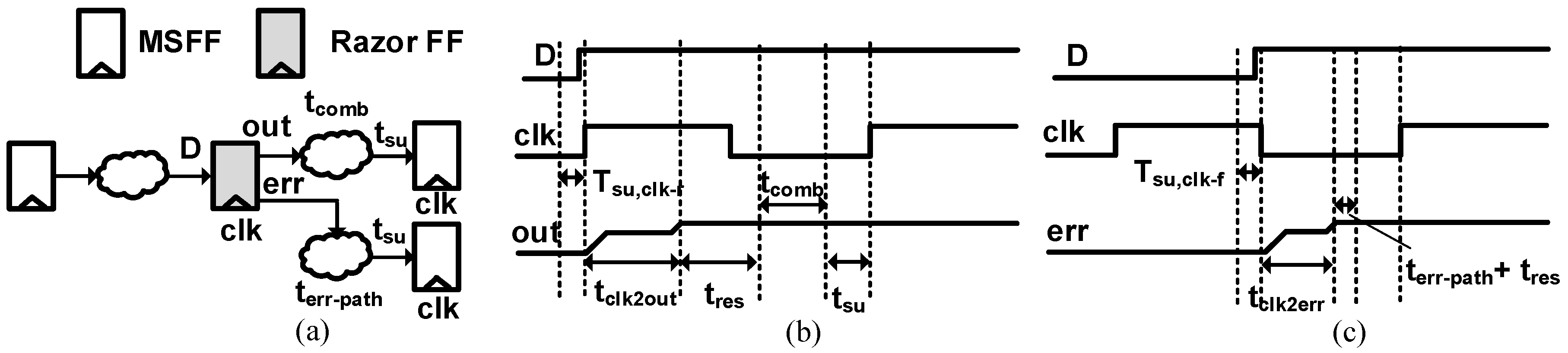
Speculative techniques relax max delay and constrain min delay by Tclk/2. The max delay savings is minimal if we consider error handling and min delay overheads. For a typical speculative pipeline shown in Figure 15, the max delay, Tmax can be speculated up to Tclk/2 till the falling edge of the clock and is calculated as:
where Tsu,clk-f represents the setup timing of the speculative flip-flop clock falling edge. The effective max delay improvement Tmax,eff is limited by the critical operating point and is calculated as:
where Tcop represents the effective amount by which max delay is relaxed till the critical operating point. The min delay requirement, Tmin, for Razor is tightened by Tclk/2 and is calculated as:
where Th,clk-f represents the hold timing requirement of the speculative clock falling edge. Thus, for a max delay improvement of Tcop, there is a min delay buffer overhead of Tclk/2.
Tmax = Tclk + Tclk/2 − Tsu,clk-f,
Tmax,eff = Tclk + Tcop − Tsu,clk-f,
Tmin = Tclk/2 + Th,clk-f,
SBFF relaxes the max delay and tightens the min delay of the critical fan-in logic by TB proportional to the consecutive stage slack as shown in Figure 16. The SBFF max delay, Tmax,SBFF, is calculated as:
where Tsu,clk_del-r represents the setup time constraint with respect to SBFF delayed clock rising edge. The max delay improvement of TB gives extra room for power, area and performance improvement. For high performance designs, the extra margin can be used to scale frequency. For low power designs, the extra margin can be used to under design the logic to achieve power and area savings. The logic downsizing makes sure that the short path delay also increases by TB, thus eliminating the need for additional hold buffers. The SBFF min delay, Tmin,SBFF, is calculated as:
where Th,clk_del-r represents the hold timing requirement with respect to the SBFF delayed clock edge. As long as the TB constraint is satisfied, the D input meets the worst-case setup timing of the delayed clock. This eliminates the need for error correction. We can represent the maximum delay constraint on TB as:
Tmax,SBFF = Tclk + TB − Tsu,clk_del-r,
Tmin,SBFF = TB + Th,clk_del-r,
TBmax,SBFF ≤ Tclk/2 − Tsu,clk_del-r,
Runtime dynamic timing speculation techniques have metastability risks at the clock edges along the data path and error path. Data path metastability will arise if D input changes too close to the positive clock edge due to voltage scaling or PVT variations, as depicted in Figure 15b. As a statistical measure of the reliability from metastable errors, we express the Mean time between failures, MTBFdata-path, as:
Here, tres represents the resolution time to exit the metastable state; T0 is the metastability window; τc is the metastability resolution time constant; fdat is the frequency of data transition; and fclk is the clock frequency. The metastability resolution time tres can be calculated as:
Here, tclk2out is the clock to output delay of the flip-flop; tcomb is the combinational logic delay of the succeeding stage; and tsu is the setup time constraint of the subsequent flip-flop as shown in Figure 15b. A higher tres amounts to better protection from metastable errors. For the speculative flip-flop, tclk2out is worse than the conventional flip-flops due to the redundant latch, which makes tres smaller. This introduces additional constraints on the combinational delay of the next pipeline stage. The error path is also prone to metastability because the dynamic voltage scaling pushes the data too close to the negative clock edge, as shown in Figure 15c. The corresponding mean time between failures, MTBFerr-path, is represented as:
Here, tres represents the resolution time to exit the metastable state; T0 is the metastability window; τc is the metastability resolution time constant; fdat is the frequency of data transition; and fclk is the clock frequency, all with respect to the error path. The error path metastability can be fatal especially since speculative designs rely on the error signal timing for proper error recovery. Here, the metastability resolution time tres can be expressed as:
Here, tclk2err is the clock to output delay for the error output signal with respect to the negative clock edge. As shown in Figure 15c, the tres window for the error path is too small, and this puts additional constraints on the error path delay terr-path. Resolution time can extend up to three clock cycles, which means the error signal will take three clock cycles to resolve fully in the event of metastability. Any timing issues along the error path will affect the error recovery process, and the system may not be able to get back to the normal error-free state. The mean time between failures for the SBFF data path can be represented as:
Here, tres represents the resolution time to come out of the metastable state; T0 is the metastability window of the delayed clock edge; τc is the metastability resolution time constant; fdata is the frequency of data transition; and fclk is the clock frequency. The metastability resolution time tres can be calculated as:
Here, tclk_del2out is the clock to output delay of the SBFF; tcomb is the combinational logic delay succeeding the SBFF; and tsu is the setup time constraint of the subsequent flip-flop, as shown in Figure 16b. Timing constraints in (6) make sure that the setup constraints are met with the delayed clock edge, and so, the probability of metastable errors is very low. The absence of metastability makes tclk_del2out smaller than tclk2out of speculative FF, which results in more resolution time for SBFF in the event of any timing upset. The design margin improvement using the proposed non-speculative approach is reliable and predictable, which results in less overhead compared to real-time design margin speculation.
MTBFdata-path = exp(tres/τc)/(fdata. T0. fclk),
tres = Tclk − tclk2out − tcomb − tsu,
MTBFerr-path = exp(tres/τc)/(fdata. T0. fclk),
tres = Tclk − TB − tclk2err − tcomb − tsu,
MTBFdata-path,SBFF = exp(tres/τc)/(fdata. T0. fclk),
tres,SBFF = Tclk − tclk_del2out − tcomb − tsu,
4. Power Optimization Algorithm
Slack balancing flip-flops help to redistribute available slack in the design to the critical stages. Once we replace the critical endpoints with SBFFs, we can leverage the additional slack to under design the critical fan-in logic. The proposed power optimization approach uses the available slack margin to downsize the critical fan-in logic. There is an area reduction and delay increase when we downsize the gates. However, the critical endpoints absorb this delay increase because the delayed data are safely captured by the delayed clock of the SBFF. This results in fewer resources along the critical fan-in logic, leading to power and area savings with respect to the baseline design. To realize this, we propose a slack analysis and downsizing (SizeOpt) algorithm as described in Algorithm 1. The procedure takes an input netlist to calculate slack available in the logic stages. Based on the timing analysis results, we filter the critical endpoints whose slack margin is less than a predefined threshold (Th). We set Th as two percent of the clock period in this work. Our timing analysis showed enormous slack presence in the logic stages. Here, the time borrowing capability of a critical path is solely based on the slack present in the consecutive stage. Therefore, we divided the available slack into four time borrow bands TB = {TB1, TB2, TB3, TB4}, which are multiples of Tclk/8 and take values TB1 = Tclk/8, TB2 = 2Tclk/8, TB3 = 3Tclk/8 and TB4 = 4Tclk/8, respectively. Depending on whether the consecutive slack in the second stage falls in TB1, TB2, TB3 or TB4, we relax the endpoint’s fan-in logic by the respective TB. This is done by adjusting the path delay during synthesis. Once the path delay is adjusted, we resynthesize the pipeline, which results in logic downsizing. The critical endpoints in the netlist are then replaced by an SBFF using custom scripts. Clock delays for the SBFFs are decided based on their time borrowing capability TB. For the best overall power/area savings, we start from the paths with the highest slack in the range of TB4. We replace those paths with SBFFs and relax their timing with path adjust commands in the synthesis stage. This process is continued until there is no more critical path that has at least TB1 slack from which to borrow. This makes sure that the design undergoes a path relaxation proportional to the maximum slack available.
| Algorithm 1: Slack Analysis and Downsizing (SizeOpt) |
| Input: Initial Netlist Output: Netlist with SBFF and optimized cells
|
5. Results and Analysis
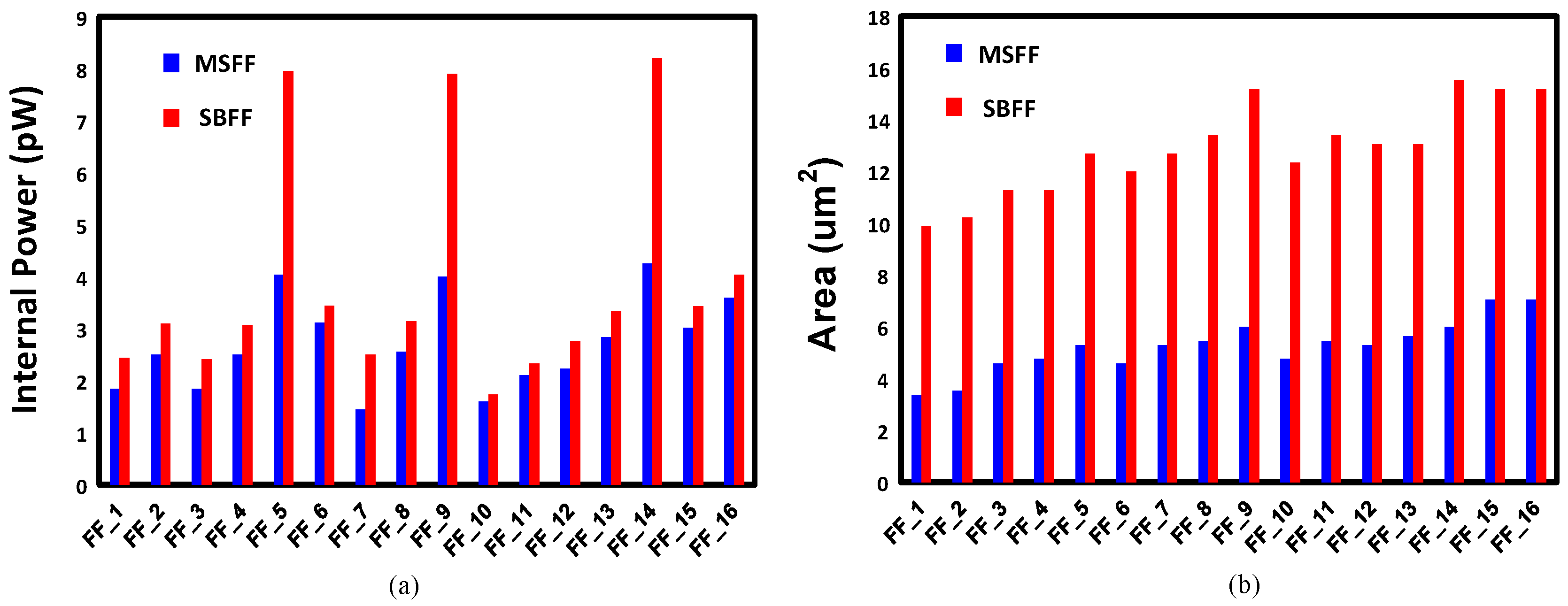
In order to enhance the processor pipeline, we developed 16 different flavors of SBFFs, as shown in Table 2. We characterized the SBFFs and compared the power, area and setup-hold time metrics with the corresponding master-slave flip-flops. Figure 17 shows the power and area comparison between the different flip-flop pairs from MSFF and SBFF library. It is evident that SBFFs consume higher power and area compared to their MSFF counterparts. However, the proposed logic downsizing helps to convert the power and area overheads to gains, unlike other resilient techniques. Figure 18 shows the timing comparison between the flip-flop pairs of the SBFF and MSFF library. The setup time and hold time are also slightly high for the SBFF cells.
Error resilience experiments were conducted on a 40-nm embedded processor with a three-stage pipeline. The whole design flow is carried out at the worst-case PVT corner using a 3σ process library, a temperature of 125 °C and a worst-case voltage of 0.99 V. The conventional worst-case corner design was used as the baseline to compare the power and area. The processor has a three-stage fetch-decode-execute pipeline, and it does more in each stage to increase the overall performance. There are no critical clock gates in the design. The processor implementation details and complexity are depicted in Table 3.
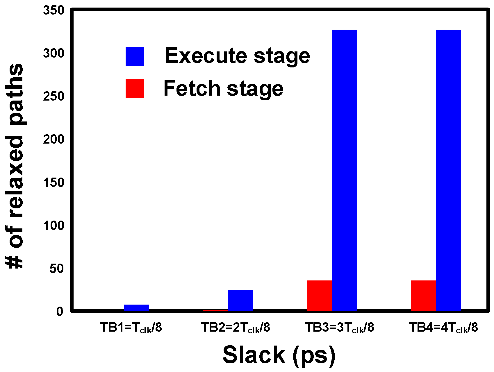
Based on the slack analysis, we found an opportunity to relax the slack margin in the data path modules shown in Figure 19. The design has ~20 K logic cells with 720 critical endpoints and 7000 flip-flops. Sixty percent of the critical endpoints have sufficient slack and can be replaced by SBFFs. The execute stage has the maximum number of critical endpoints, and ~326 paths in the execute stage are relaxed by a maximum slack margin of TB4.
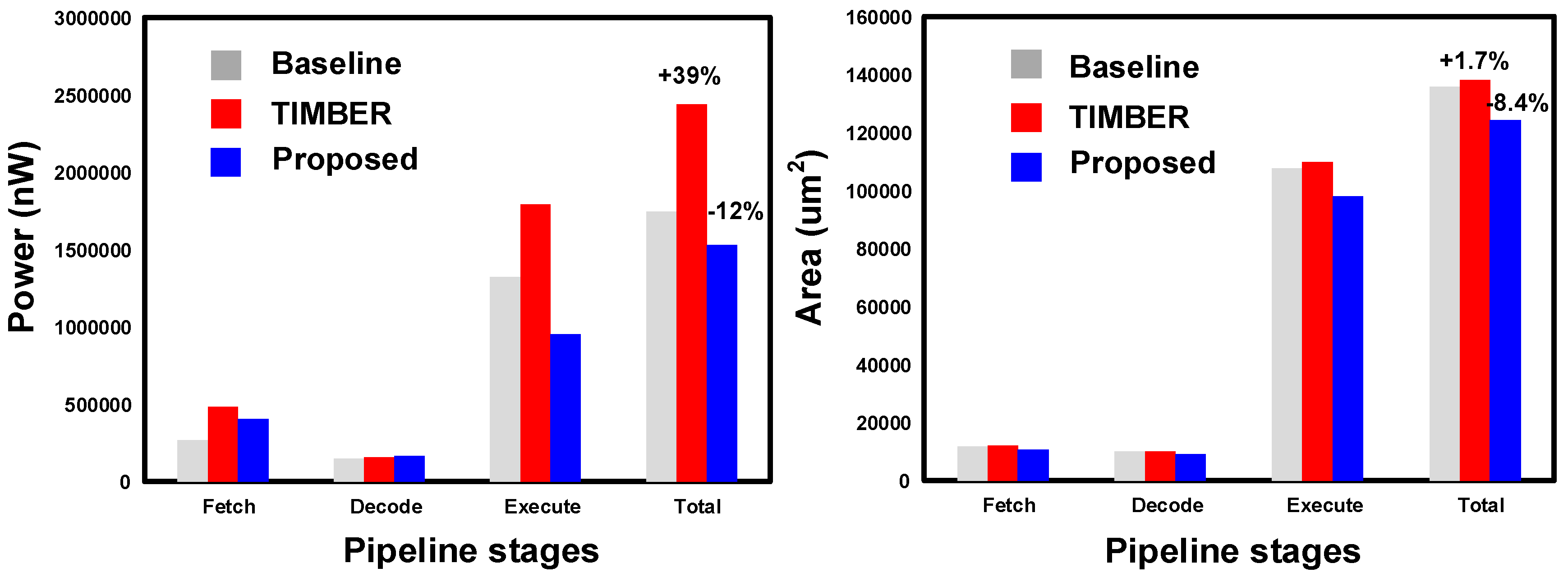
The proposed power optimization approach down-sizes the critical data paths that have SBFFs by a predefined set of relaxation margins. Here, the actual power and area savings depend on how many endpoints are relaxed and for which particular relaxation margin. Table 4 and Table 5 summarize the power and area savings of the proposed approach. Using our algorithm, we get a maximum power savings of ~12% as shown in Figure 20a. We get the maximum power savings in the execute stage, which has the maximum number of paths beings relaxed by TB4. On the contrary, a typical speculative error resilience approach like TIMBER [17] suffers from a power overhead of 39% due to the speculative hardware. We get an area savings of ~8% with the proposed approach, as shown in Figure 20b. TIMBER hardware has an area overhead of ~1.7%. Again, the area savings predominantly comes from the execute stage path relaxations. It is evident that the higher relaxation margins of TB4 give more optimization opportunity and reduce the overheads, which results in power and area savings.
6. Conclusions
In this paper, we propose a non-speculative pipe-line design methodology to relax the slack margins proportionate to the available slack using Slack Balancing Flip-Flops (SBFFs). The proposed design methodology handles worst-case variations by sampling the data at a delayed clock edge. The additional slack margin obtained from SBFFs is used to downsize the critical fan-in logic for power and area savings. Existing speculative error detection schemes have critical operating point behavior, and their effectiveness largely depends on the error rate at any given point of time. The proposed approach is non-speculative, which eliminates the critical wall of slack behavior. The speculative techniques need to be periodically tuned to adapt to the ambient operating conditions and workload. They rely on run-time voltage scaling, which results in metastability issues and compromises the functionality of the chip. The deterministic timing closure used in the proposed approach eliminates metastability and error correction overheads. Moreover, the proposed logic downsizing eliminates the need for hold buffers. Experimental results of the proposed design methodology show a power and area savings of 12% and 8%, respectively, compared to the worst-case design.
With the aim to maximize power and area benefits, the resilient design proposed can be improved using dynamic variation tolerance approaches. In the future, the proposed design time resilience technique can be combined with runtime voltage/frequency scaling to reap more benefits. Furthermore, we can train the circuit to enable or disable time borrowing depending on the data activity rates. This will help to reduce the redundancy overheads associated the with the time borrowing hardware.
Acknowledgments
This work was supported by EDB-Industrial Post-graduate Programme, Singapore, and NXP Semiconductors, Singapore.
Author Contributions
The main author, Mini Jayakrishnan, carried out the experiments and writing of the paper. Alan Chang recommended the idea/topic and provided the necessary platform to conduct the experiments. Tony Tae-Hyoung Kim guided the main author in the research and documentation.
Conflicts of Interest
The authors declare no conflict of interest.
References
- Borkar, S.; Karnik, T.; Narendra, S.; Tschanz, J.; Keshavarzi, A.; De, V. Parameter Variations and Impact on Circuits and Microarchitecture. In Proceedings of the 40th Annual Design Automation Conference (DAC), Anaheim, CA, USA, 2–6 June 2003. [Google Scholar]
- Ghosh, S.; Roy, K. Parameter variation tolerance and error resiliency: New design paradigm for the nanoscale era. Proc. IEEE 2010, 98, 1718–1751. [Google Scholar] [CrossRef]
- Asenov, A.; Brown, A.R.; Davies, J.H.; Kaya, S.; Slavcheva, G. Simulation of intrinsic parameter fluctuations in decananometer and nanometer-scale MOSFETs. IEEE Trans. Electron Devices 2003, 50, 1837–1852. [Google Scholar] [CrossRef]
- Nassif, S.R. Modeling and analysis of manufacturing variations. In Proceedings of the Custom Integrated Circuit Conference, San Diego, CA, USA, 9 May 2001. [Google Scholar]
- Borkar, S. Designing Reliable Systems from Unreliable Components: The Challenges of Transistor Variability and Degradation. IEEE Micro 2005, 25, 10–16. [Google Scholar] [CrossRef]
- Bowman, K.A.; Duvall, S.G.; Meindl, J.D. Impact of Die-to-Die and With-in-Die Parameter Fluctuations on the Maximum Clock Frequency Distribution for Gigascale Integration. IEEE J. Solid State Circuits 2002, 37, 183–190. [Google Scholar] [CrossRef]
- Dreslinski, R.G.; Wieckowski, M.; Blaauw, D.; Sylvester, D.; Mudge, T. Near-Threshold Computing: Reclaiming Moore’s Law through Energy Efficient Integrated Circuits. Proc. IEEE 2010, 98, 253–266. [Google Scholar] [CrossRef]
- Meijer, M.; Liu, B.; van Veen, R.; de Gyvez, J.P. Post-Silicon Tuning Capabilities of 45 nm Low-Power CMOS Digital Circuits. In Proceedings of the Symposium on VLSI Circuits, Kyoto, Japan, 16–18 June 2009. [Google Scholar]
- Kim, T.; Persaud, R.; Kim, C.H. Silicon odometer: An on-chip reliability monitor for measuring frequency degradation of digital circuits. In Proceedings of the Very Large Scale Integration (VLSI) Circuits Symposium, Kyoto, Japan, 14–16 June 2007. [Google Scholar]
- Gupta, P.; Agarwal, Y.; Dolecek, L.; Dutt, N.; Gupta, R.K.; Kumar, R.; Mitra, S.; Nicolau, A.; Rosing, T.S.; Srivastava, M.B.; et al. Underdesigned and Opportunistic Computing in Presence of Hardware Variability. IEEE Trans. Comput.-Aided Des. Integr. Circuits Syst. 2013, 32, 8–23. [Google Scholar] [CrossRef]
- Tschanz, J.; Bowman, K.; Walstra, S.; Agostinelli, M.; Karnik, T.; De, V. Tunable Replica Circuits and Adaptive Voltage-Frequency Techniques for Dynamic Voltage, Temperature, and Aging Variation Tolerance. In Proceedings of the Symposium on VLSI Circuits, Kyoto, Japan, 16–18 June 2009. [Google Scholar]
- Ernst, D.; Kim, N.S.; Das, S.; Pant, S.; Rao, R.; Pham, T.; Ziesler, C.; Blaauw, D.; Austin, T.; Mudge, T.; et al. Razor: A Low-Power Pipeline Based on Circuit-Level Timing Speculation. In Proceedings of the 36th Symposium on Microarchitecture (MICRO-36), San Diego, CA, USA, 3–5 December 2003. [Google Scholar]
- Das, S.; Tokunaga, C.; Pant, S.; Ma, W.; Kalaiselvan, S.; Lai, K.; Bull, D.; Blaauw, D. Razor II: In Situ Error Detection and Correction for PVT and SER Tolerance. IEEE J. Solid-State Circuits 2009, 44, 32–48. [Google Scholar] [CrossRef]
- Bowman, K.; Tschanz, J.; Kim, N.; Lee, J.; Wilkerson, C.; Lu, S.; Karnik, T.; De, V. Energy-Efficient and Metastability-Immune Resilient Circuits for Dynamic Variation Tolerance. IEEE J. Solid-State Circuits 2009, 44, 49–63. [Google Scholar] [CrossRef]
- Fojtik, M.; Fick, D.; Kim, Y.; Pinckney, N.; Harris, D.M.; Blaauw, D.; Sylvester, D. Bubble Razor: Eliminating timing margins in an ARM cortex-M3 processor in 45 nm CMOS using architecturally independent error detection and correction. IEEE J. Solid-State Circuits 2013, 48, 66–81. [Google Scholar] [CrossRef]
- Joshi, V.; Blaauw, D.; Sylvester, D. Soft-edge flip-flops for improved timing yield: Design and optimization. In Proceedings of the IEEF/ACM International Conference on Computer-Aided Design, San Jose, CA, USA, 5–8 November 2007. [Google Scholar]
- Choudhury, M.; Chandra, V.; Mohanram, K.; Aitken, R. TIMBER: Time borrowing and error relaying for online timing error resilience. In Proceedings of the Design, Automation & Test in Europe Conference & Exhibition (DATE), Dresden, Germany, 8–12 March 2010. [Google Scholar]
- Bull, D.; Das, S.; Shivashankar, K.; Dasika, G.; Flautner, K.; Blaauw, D. A power-efficient 32-bit ARM processor using timing-error detection and correction for transient-error tolerance and adaptation to PVT variation. IEEE J. Solid-State Circuits 2011, 46, 18–31. [Google Scholar] [CrossRef]
- Das, S.; Roberts, D.; Lee, S.; Pant, S.; Blaauw, D.; Austin, T.; Flautner, K.; Mudge, T.T. A self-tuning DVS processor using delay error detection and correction. IEEE J. Solid-State Circuits 2006, 41, 792–804. [Google Scholar] [CrossRef]
- Austin, T.; Bertacco, V.; Blaauw, D.; Mudge, T. Opportunities and Challenges for Better Than Worst-Case Design. In Proceedings of the Asia and South Pacific Design Automation Conference, Shanghai, China, 18–21 January 2005. [Google Scholar]
- Liu, X.; Papaefthymiou, M.C.; Friedman, E.G. Maximizing performance by retiming and clock skew scheduling. In Proceedings of the 36th Design Automation Conference, New Orleans, LA, USA, 21–25 June 1999. [Google Scholar]
- Monteiro, J.; Devadas, S.; Ghosh, A. Retiming sequential circuits for low power. In Proceedings of the IEEE/ACM International Conference on Computer-Aided Design, Santa Clara, CA, USA, 7–11 November 1993. [Google Scholar]
- Neves, J.L.; Friedman, E.G. Optimal clock skew scheduling tolerant to process variations. In Proceedings of the 33rd Annual Design Automation Conference, Las Vegas, NV, USA, 3–7 June 1996. [Google Scholar]
- Sathyamurthy, H.; Sapatnekar, S.; Fishburn, J. Speeding up pipelined circuits through a combination of gate sizing and clock skew optimization. IEEE Trans. Comput. Aided Des. Integr. Circuits Syst. 1998, 17, 173–182. [Google Scholar] [CrossRef]
- Xi, J.G.; Dai, W.W.M. Useful-skew clock routing with gate sizing for low power design. In Proceedings of the 33rd Annual Design Automation Conference, Las Vegas, NV, USA, 3–7 June 1996. [Google Scholar]
- Sarangi, S.R.; Greskamp, B.; Tiwari, A.; Torrellas, J. EVAL: Utilizing processors with variation-induced timing errors. In Proceedings of the International Symposium on Microarchitecture, Lake Como, Italy, 8–12 November 2008. [Google Scholar]
- Greskamp, B.; Wan, L.; Karpuzcu, W.R.; Cook, J.J.; Torrellas, J.; Chen, D.; Zilles, C. BlueShift: Designing Processors for Timing Speculation from the Ground Up. In Proceedings of the IEEE International Symposium on High Performance Computer Architecture, Raleigh, NC, USA, 14–18 February 2009. [Google Scholar]
- Patel, J. CMOS Process Variations: A Critical Operation Point Hypothesis. Available online: https://web.stanford.edu/class/ee380/Abstracts/080402-jhpatel.pdf (accessed on 19 March 2018).
- Kahng, A.B.; Kang, S.; Li, J. A New Methodology for Reduced Cost of Resilience. In Proceedings of the GLSVLSI, Houston, TX, USA, 21–23 May 2014. [Google Scholar]
- Alidash, H.K.; Oklobdzija, V.G. Low-power soft error hardened latch. J. Low Power Electron. Appl. 2010, 6, 218–226. [Google Scholar] [CrossRef]
- Paik, S.; Nam, G.J.; Shin, Y. Implementation of pulsed-latch and pulsed-register circuits to minimize clocking power. In Proceedings of the International Conference on Computer-Aided Design, San Jose, CA, USA, 7–10 November 2011. [Google Scholar]
- Sartori, J.; Kumar, R. Characterizing the Voltage Scaling Limitations of Razor-Based Designs; Technical Report; Coordinated Science Laboratory, The University of Illinois at Urbana-Champaign: Champaign, IL, USA, 2009. [Google Scholar]
- Wirnshofer, M. A Variation-Aware Adaptive Voltage Scaling Technique Based on In-Situ Delay monitoring. In Proceedings of the IEEE International Symposium on Design and Diagnostics of Electronic Circuits and Systems, Cottbus, Germany, 13–15 April 2012. [Google Scholar]
- Ghosh, S.; Martin, S.; Stelmach, S. Reliability for IoT and Automotive markets. In Proceedings of the System-on-Chip Conference (SOCC), Munich, Germany, 5–8 September 2017. [Google Scholar]
- Jayakrishnan, M.; Chang, A.; De Gyvez, J.P.; Hyoung, K.T. Slack-aware Timing Margin Redistribution Technique Utilizing Error Avoidance Flip-Flops and Time Borrowing. In Proceedings of the IFIP/IEEE International Conference on Very Large-Scale Integration (VLSI-SoC), Daejeon, Korea, 5–7 October 2015. [Google Scholar]
Figure 1.
Speculative techniques: (a) Razor I error detection with flip-flop as the data path [12]; (b) Razor II error detection with latch as the data path [13] and (c) TIMBER error masking with flip-flop as the data path [17].
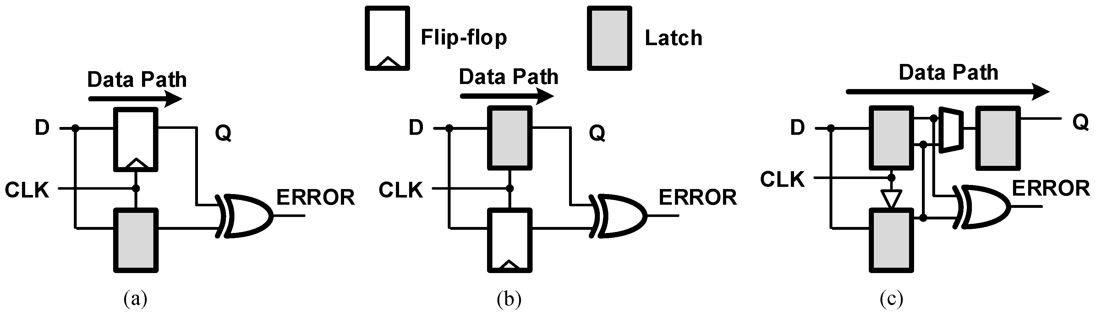
Figure 2.
Reclaimed slack vs. error rate for various resilience techniques.
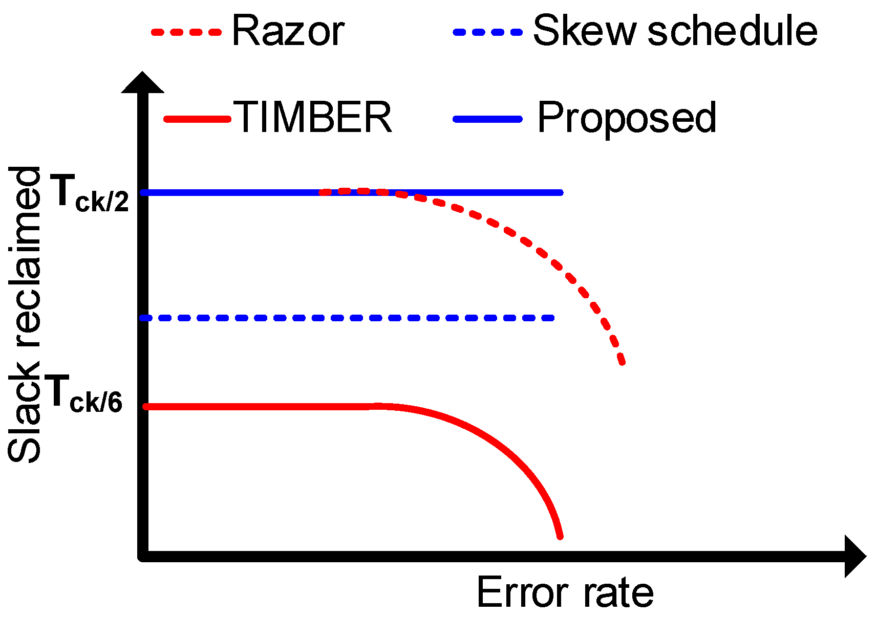
Figure 3.
Comparison of design margining techniques: (a) Worst-Case Design (WCD) margining and (b) Opportunistic Better-Than-Worst-Case (OBTWC) design margining.
Figure 3.
Comparison of design margining techniques: (a) Worst-Case Design (WCD) margining and (b) Opportunistic Better-Than-Worst-Case (OBTWC) design margining.
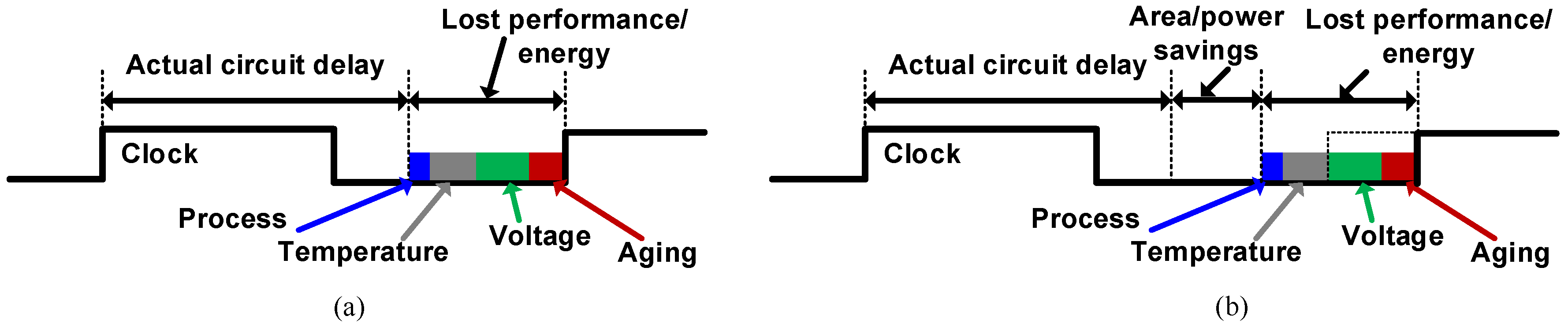
Figure 4.
Slack histogram of the processor pipeline (a) in the worst case, (b) with 20-mV voltage scaling and (c) with 40-mV voltage scaling.
Figure 4.
Slack histogram of the processor pipeline (a) in the worst case, (b) with 20-mV voltage scaling and (c) with 40-mV voltage scaling.

Figure 5.
Cost of resilience and voltage scaling trade-off.

Figure 6.
Critical path slacks (pipe_1) and consecutive stage slacks (pipe_2) of the processor.

Figure 7.
A circuit example and timing graph to explain slack balancing.
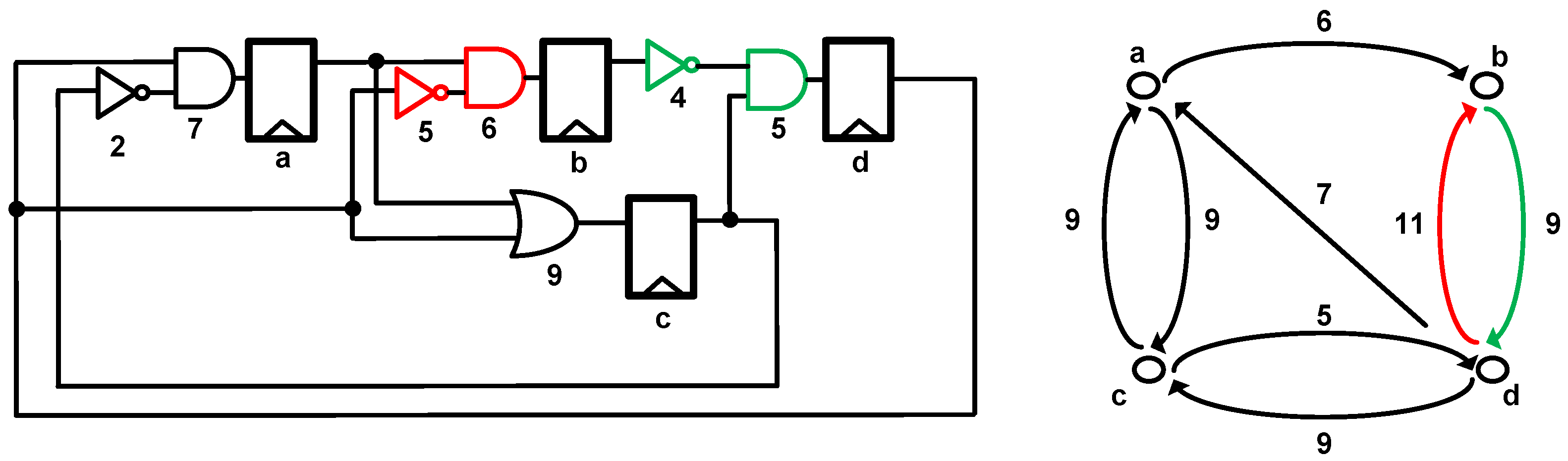
Figure 8.
Speculative power-aware flip-flop: (a) slack margin at sign off; (b) slack margin relaxed with timing speculation flip-flop and (c) slack margin traded off with power. P1, Path 1.
Figure 8.
Speculative power-aware flip-flop: (a) slack margin at sign off; (b) slack margin relaxed with timing speculation flip-flop and (c) slack margin traded off with power. P1, Path 1.

Figure 9.
Performance-aware optimizations: (a) slack margin at sign off; (b) slack margin relaxed with clock skew scheduling and gate sizing and (c) slack margin traded off with frequency.
Figure 9.
Performance-aware optimizations: (a) slack margin at sign off; (b) slack margin relaxed with clock skew scheduling and gate sizing and (c) slack margin traded off with frequency.

Figure 10.
Proposed SBFF: (a) slack margin at sign off, (b) slack margin relaxed with SBFF and (c) slack margin used to downsize logic.
Figure 10.
Proposed SBFF: (a) slack margin at sign off, (b) slack margin relaxed with SBFF and (c) slack margin used to downsize logic.
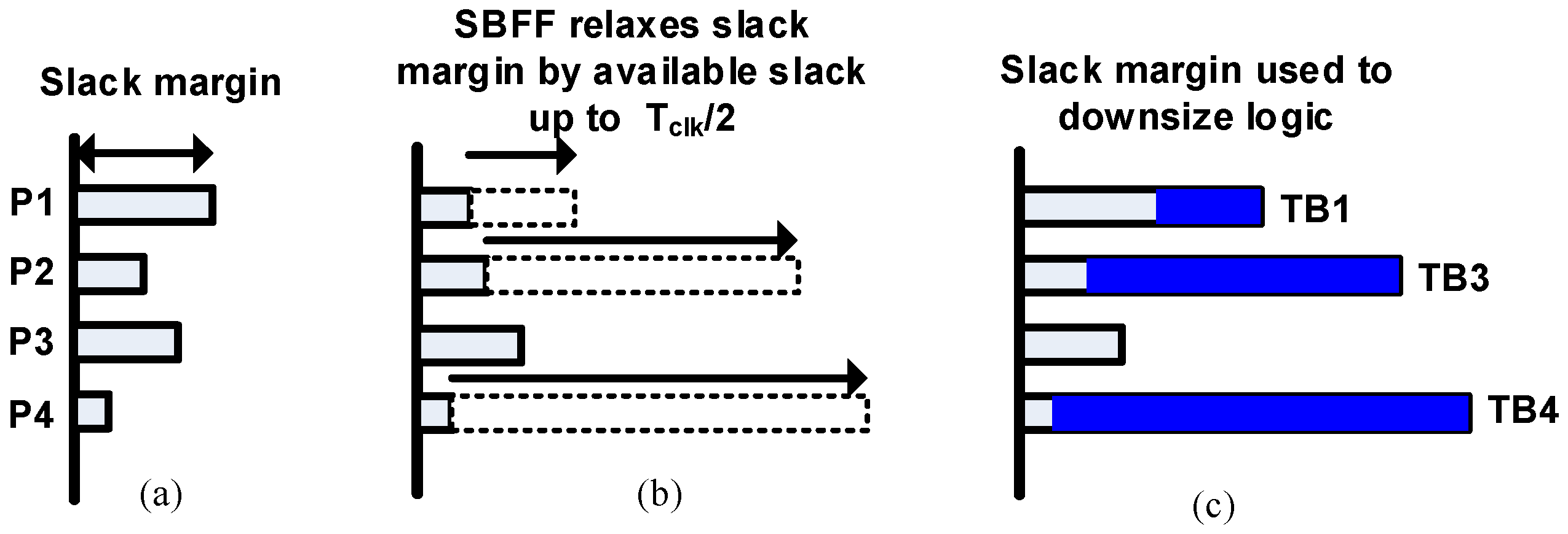
Figure 11.
(a) SBFF and (b) timing diagram. DCK, Delayed Clock.

Figure 12.
SBFF simulation result.

Figure 13.
Data activity monitoring in SBFF. (a) Intermittent triggering of the activity monitor with low data activity and (b) continuous triggering of activity monitor with high data activity.
Figure 13.
Data activity monitoring in SBFF. (a) Intermittent triggering of the activity monitor with low data activity and (b) continuous triggering of activity monitor with high data activity.
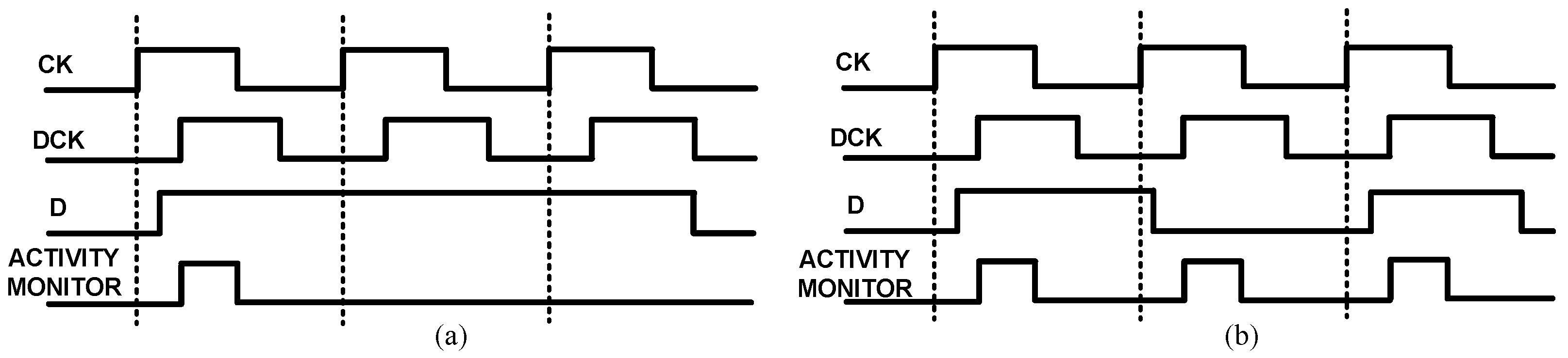
Figure 14.
Design flow using SBFF.

Figure 15.
(a) Speculative flip-flop pipeline, (b) data path metastability and (c) error path metastability.
Figure 15.
(a) Speculative flip-flop pipeline, (b) data path metastability and (c) error path metastability.

Figure 16.
(a) SBFF pipeline and (b) data path timing.

Figure 17.
(a) Power comparison between MSFF and SBFF standard cells and (b) area comparison between MSFF and SBFF standard cells.
Figure 17.
(a) Power comparison between MSFF and SBFF standard cells and (b) area comparison between MSFF and SBFF standard cells.

Figure 18.
(a) Setup time comparison between MSFF and SBFF standard cells and (b) hold time comparison between MSFF and SBFF standard cells.
Figure 18.
(a) Setup time comparison between MSFF and SBFF standard cells and (b) hold time comparison between MSFF and SBFF standard cells.
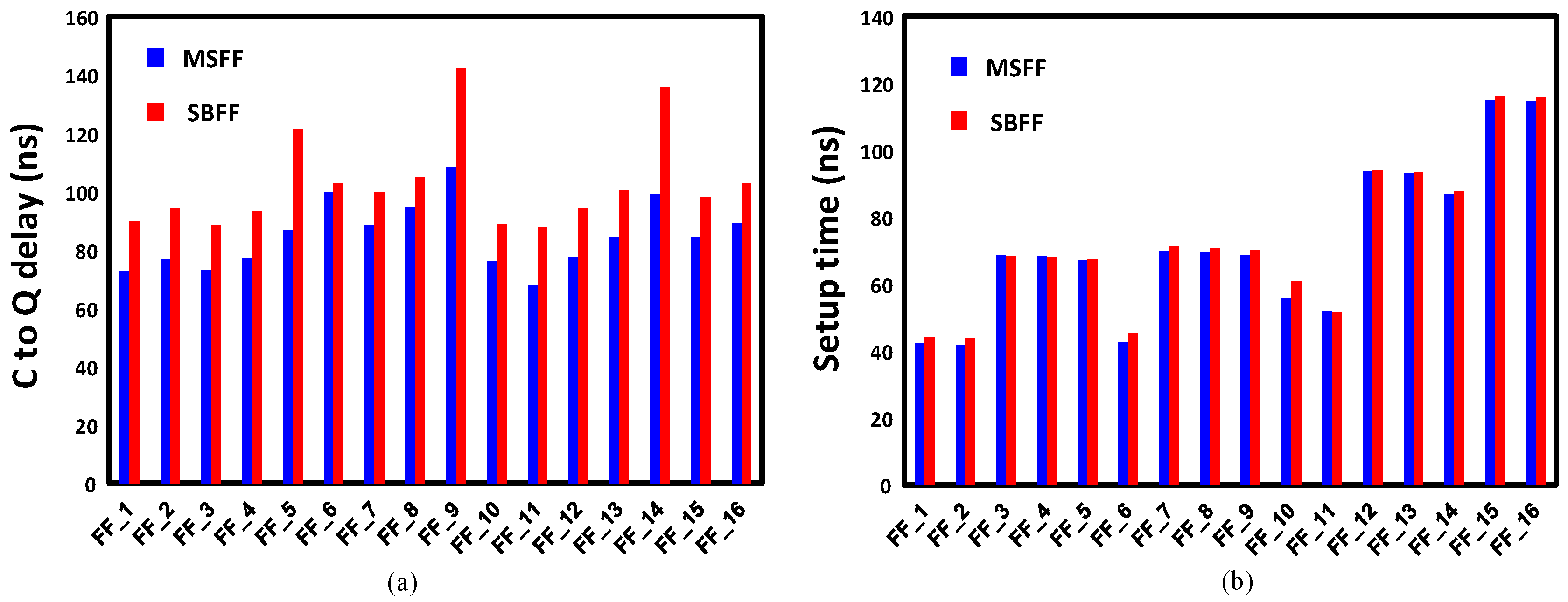
Figure 19.
Slack improvement in the pipeline stages.

Figure 20.
SizeOpt power optimization technique. (a) Power savings and (b) area savings with respect to the worst-case design.
Figure 20.
SizeOpt power optimization technique. (a) Power savings and (b) area savings with respect to the worst-case design.


Table 1.
Comparison of cost-effective resilient design techniques. DSTB, Double Sampling with Time Borrowing; TDTB, Detection with Time Borrowing; SBFF, Slack Balancing Flip-Flops.
Table 1.
Comparison of cost-effective resilient design techniques. DSTB, Double Sampling with Time Borrowing; TDTB, Detection with Time Borrowing; SBFF, Slack Balancing Flip-Flops.
| Feature | Speculative | Non-Speculative | |||
|---|---|---|---|---|---|
| Techniques | EVAL [26], Blueshift [27] | Razor [12], DSTB, TDTB [14], TIMBER [17], soft edge flip-flop [16] | SlackOptimizer, SkewOptimizer, CombOpt [29] | Retiming [21], skew scheduling [23], gate sizing [24] | Proposed SBFF + logic downsizing |
| Trade-off | Error rate vs. performance | Error rate vs. power | Error rate vs. power | No | No |
| Error handling | Duplicate paths | Duplicate Latch/FFs | Duplicate Latch/FFs | No error | No error |
| Clock tree loading | No | Yes | Yes | No | Yes |
| Short path padding | No | Yes | Yes | Yes | No |
| Metastability | Yes | Yes | Yes | No | No |
| Sequential overhead | Large | Large | Large | Small | Large |
| Combinational overhead | Large | Small | Large | Small | Small |
| Area overhead | Yes | Yes | Yes | Yes | No |
| Margin relaxation | Small | Up to Tck/2 | Tck/2 | Small | Tck/2 |
MS = Meta Stability, Tck = clock period.
Table 2.
SBFF flavors used in the proposed design methodology.
| Reference | Drive Strength | Description |
|---|---|---|
| FF_1, FF_2 | 1X, 2X | D-flip-flop, positive-edge triggered, q-only |
| FF_3, FF_4, FF_5 | 1X, 2X, 8X | D-flip-flop, positive-edge triggered, q-only |
| FF_6 | 1X | D-flip-flop, positive-edge triggered, low-asynchronous-clear, q-only |
| FF_7, FF_8, FF_9 | 1X, 2X, 8X | D-flip-flop, positive-edge triggered, low-asynchronous-clear, q-only |
| FF_10, FF_11 | 1X, 2X | D-flip-flop, positive-edge triggered, low-asynchronous-clear/set, q-only |
| FF_12, FF_13, FF_14 | 1X, 2X, 8X | D-flip-flop, positive-edge triggered, low-asynchronous-clear/set, q-only |
| FF_15, FF_16 | 1X, 2X, 8X | D-flip-flop, positive-edge triggered, low-asynchronous-clear/set, sync hold, q-only |
Table 3.
Implementation details of the proposed design.
| Technology Node | 40 nm |
|---|---|
| Std. cells: | ~50 K-gates |
| Flip-flops | ~7000 |
| Memory: | 32 KB ISRAM, 32 KB DSRAM |
| 4 KB ROM | |
| Max. Frequency | 180 MHz |
| Typ. Voltage | 1.1 Volts |
Table 4.
Power savings of the proposed design methodology.
| Power (nW) | Baseline | TIMBER [17] | Proposed | |||||||||
|---|---|---|---|---|---|---|---|---|---|---|---|---|
| #Cells | Leakage | Dynamic | Total | #Cells | Leakage | Dynamic | Total | #Cells | Leakage | Dynamic | Total | |
| Fetch | 1976 | 1463 | 265,127 | 266,590 | 2014 | 1481 | 482,389 | 483,870 | 1751 | 1103 | 401,268 | 402,372 |
| Decode | 1874 | 920 | 149,114 | 150,034 | 1900 | 805 | 154,762 | 155,567 | 1796 | 573 | 162,912 | 163,485 |
| Execute | 16,414 | 14,825 | 1,307,869 | 1,322,695 | 16,356 | 14,714 | 1,777,447 | 1,792,162 | 15,053 | 11,039 | 941,299 | 952,339 |
Table 5.
Area savings of the proposed design methodology.
| Area (µm2) | Baseline | TIMBER [17] | Proposed | |||||||||
|---|---|---|---|---|---|---|---|---|---|---|---|---|
| #Cells | Cell Area | Net Area | Total | #Cells | Cell Area | Net Area | Total | #Cells | Cell Area | Net Area | Total | |
| Fetch stage | 1976 | 4980 | 6714 | 11,695 | 2014 | 5217 | 6928 | 12,145 | 1751 | 4391 | 6236 | 10,627 |
| Decode stage | 1874 | 3316 | 6640 | 9955 | 1900 | 3264 | 6677 | 9940 | 1796 | 2768 | 6430 | 9199 |
| Execute stage | 16,414 | 44,741 | 62,899 | 107,639 | 16,356 | 46,919 | 62,784 | 109,702 | 15,053 | 39,790 | 58,245 | 98,034 |
© 2018 by the authors. Licensee MDPI, Basel, Switzerland. This article is an open access article distributed under the terms and conditions of the Creative Commons Attribution (CC BY) license (http://creativecommons.org/licenses/by/4.0/).
Share and Cite
MDPI and ACS Style
Jayakrishnan, M.; Chang, A.; Kim, T.T.-H. Opportunistic Design Margining for Area and Power Efficient Processor Pipelines in Real Time Applications. J. Low Power Electron. Appl. 2018, 8, 9. https://doi.org/10.3390/jlpea8020009
AMA Style
Jayakrishnan M, Chang A, Kim TT-H. Opportunistic Design Margining for Area and Power Efficient Processor Pipelines in Real Time Applications. Journal of Low Power Electronics and Applications. 2018; 8(2):9. https://doi.org/10.3390/jlpea8020009
Chicago/Turabian StyleJayakrishnan, Mini, Alan Chang, and Tony Tae-Hyoung Kim. 2018. "Opportunistic Design Margining for Area and Power Efficient Processor Pipelines in Real Time Applications" Journal of Low Power Electronics and Applications 8, no. 2: 9. https://doi.org/10.3390/jlpea8020009
Note that from the first issue of 2016, this journal uses article numbers instead of page numbers. See further details here.