Review

Mastering the Art of High Mobility Material Integration on Si: A Path towards Power-Efficient CMOS and Functional Scaling

Imec, Kapeldreef 75, 3001 Heverlee, Belgium
J. Low Power Electron. Appl. 2016, 6(2), 9; https://doi.org/10.3390/jlpea6020009
Submission received: 31 March 2016 / Revised: 16 May 2016 / Accepted: 6 June 2016 / Published: 14 June 2016
(This article belongs to the Special Issue Selected Papers from IEEE S3S Conference 2015)

Abstract

:
In this work, we will review the current progress in integration and device design of high mobility devices. With main focus on (Si)Ge for PMOS and In(Ga)As for NMOS, the benefits and challenges of integrating these materials on a Si platform will be discussed for both density scaling (“more Moore”) and functional scaling to enhance on-chip functionality (“more than Moore”).

1. Introduction

Over the last years, new trends and applications have emerged which will have large economical and societal impact: new computing paradigms like neuromorphic [1] and quantum computing [2], big data and internet-of-things (IoT) [3]. New functionalities will be needed and the key enabling circuits and systems will require a variety of different devices and technologies co-integrated on the same platform. At the core of the hardware innovations will be new process technologies that not only allow for more power-efficient CMOS transistors but also specialized devices to enable new on-chip functionality, e.g., RF/analog, near-threshold Logic, high-speed I/O, optoelectronics, etc. At the most detailed level, co-integration of different beyond-Si materials like Ge, III-V, SiGe, etc., with Si will require significant innovations in defect, stress, and process thermal budget management. In this paper, we will address these challenges and the progress made to overcome them. Moreover, we will elaborate on the advantages of using these materials for both extending density scaling and increasing on-chip functionality.

2. High Mobility Materials

(Si)Ge and III-V materials can intrinsically deliver higher hole and electron mobilities than Si: a bulk hole mobility of 1900 cm2/Vs [4] has been reported for Ge (versus 500 cm2/Vs in Si) and electron mobilities in InGaAs and InAs can be as high as 70,000 cm2/Vs [5]. This is especially important when scaling down the supply voltage and thus reducing the power density in advanced technologies while still being able to increase the performance at these reduced voltages [6]. The replacement of Si by high mobility materials is not without challenges: to be economically viable and since co-integration with Si devices will be necessary, these materials need to be integrated on a Si platform. The mismatch between Si and Ge is about 4%, and for III-V this can go up to 12% in the case of InAs. As such, achieving material with low defectivity is one of the key concerns. Next to that, finding a gate stack with low interface and high-k dielectric defects could be one of the show stoppers. Finally, the trade-off between performance, leakage and as such scalability will also need to be addressed for the high mobility devices.
In the next sections, we will discuss the challenges related to gate stack, material integration and device scalability. In the last technical section, we will demonstrate that beyond the typical CMOS scaling these materials could also play a very important role in enhancing the system functionality by providing very specific key components.

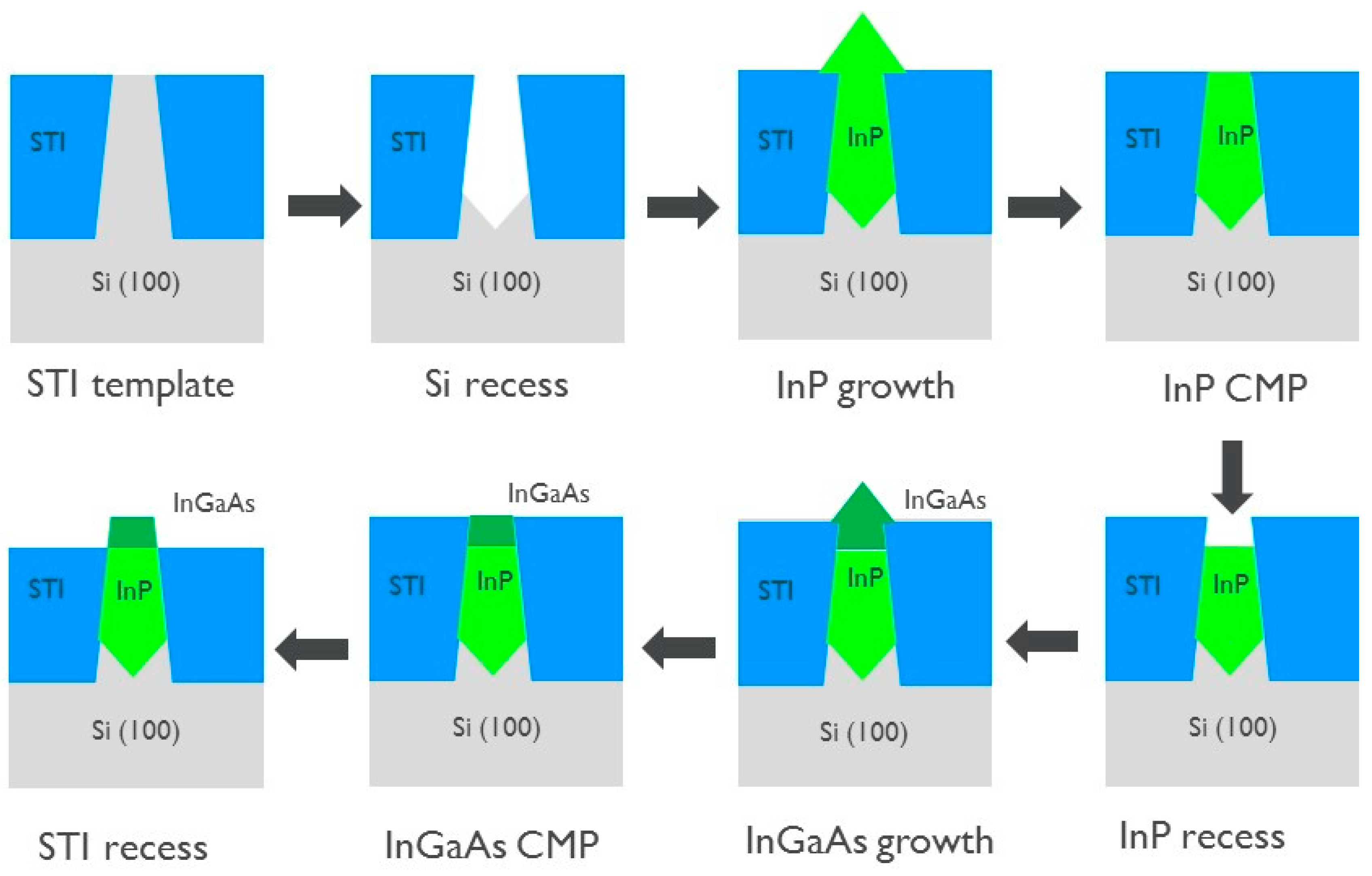
3. Ge and III-V Integration on Si Substrates

The lattice mismatch between Si and Ge is 4%. As such growing Ge directly on Si will give rise to the formation of defects which can impact both the leakage and the performance of the devices [7]. The lattice mismatch between InP and In(Ga)As with Si is even higher than for Ge, about 8% and up to 12% for InAs. Specifically, for III-V, the presence of anti-phase boundaries (APB), which occur at the interface between the non-polar (group IV) and polar (group III-V) semiconductors, can pose an even higher challenge for hetero-epitaxy of III-V on Si.
Virtual SiGe [8], Ge and III-V [9] buffer layers on bulk Si wafers have been demonstrated. Typically, 1–2 µm thick layers need to be grown and post-deposition TDD (threading dislocation density) anneals are required to lower the defect density. To date, defect densities as low as 106 cm−2 have been reported for SiGe [8]. Reported defect levels for III-V on 300 mm Si are, however, significantly higher: 1–2 × 109 cm−2 [9]. The latter substrates also require a more complex stack consisting of combinations of GaAs, InP and InAlAs to fabricate the required top InGaAs channels.
Starting from these virtual Si1-xGex buffers, either a Ge or Si1-yGey (y > x) top layer can be grown for the PMOS, thereby introducing compressive strain in the channel, while for NMOS, using the same buffer layer (common buffer), a tensile strained Si layer can be grown, thereby allowing integration of both NMOS and PMOS on the same substrate. In [10], Kian-Hui et al. demonstrated the co-integration of InAs NMOS and GaSb PMOS using an ultra-thin III-V buffer on Si. As the channel layers are introduced from the very beginning in the process flow, the thermal budget needs to be well controlled, thereby necessitating a lowering of the temperature for the Shallow Trench Isolation (STI) when planar or bulk FinFET devices are considered. In [11], 15 nm wide strained Ge FinFET devices on Si0.25Ge0.75 substrates were demonstrated using a novel low temperature STI process.
However, the high substrate cost and potential concerns with self-heating make the virtual buffer approach a lesser viable option for large scale integration. Reports [12] have shown that strained Ge FinFET devices fabricated on SiGe buffers can show up to 115% increase in temperature as compared to Si at scaled dimensions and realistic operating conditions.
An alternative way of introducing these materials is by GeOI/IIIVOI (Germanium-on-Insulator/III-V-on-Insulator) substrates [13,14]. In the case of Ge, these substrates can be fabricated either by bonding of a Ge donor wafer to an oxidized Si handle wafer or by the Ge condensation method, where a SiGe layer grown on a standard SOI (Silicon-On-Insulator) wafer is oxidized thereby turning the SiGe layer into a Ge-rich layer. Recent work by P. Hashemi et al. shows that highly performing SiGe-on-Insulator FinFET devices with fin widths below 10 nm and hole mobility around 300 cm2/Vs can be achieved for a Ge content of 71% [15]. Co-integration of III-V NMOS and Ge PMOS [16] has been demonstrated, starting from a Ge wafer and using wafer bonding to transfer the III-V layer on the common Ge substrate. Specifically, for III-V, L. Czornomaz et al. have demonstrated the Confined Epitaxial Lateral Overgrowth (CELO) technique as an alternative way to fabricate III-V on insulator substrates [17].
The latter technique is partially based on the fin replacement technique which is a more elegant solution to grow the different materials selectively in specific areas where needed. This integration scheme can be used for both (Si)Ge and III-V devices. A typical process flow, in this case for III-V, is shown in Figure 1 [18]. The process flow starts from 300 mm Si substrates. In a next step, a standard STI is fabricated, which as such makes this overall integration scheme also compatible with more advanced Self-Aligned Double (SADP) and Quadruple (SAQP) patterning schemes. The Si is then recessed using TMAH and the InP buffer layer is grown using Metal Organic Vapor Phase Epitaxy (MOVPE). The function of this layer is two-fold: firstly, all defects need to be confined in this layer in order to allow the growth of a low defective InGaAs channel layer and secondly it can be used to improve the electrostatic control because the band-offset between InP and InGaAs allows us to confine the carriers more effectively in the channel. When the InP is grown on a {111} plane after the TMAH etch, a 10 nm thick complex network of twins is formed at the interface with Si. Above this twinned region, the InP lattice is already aligned with that of the underlying Si and the generation of misfit dislocations along the channel are also avoided by initiating the growth on these Si {111} planes of the V-groove. Next to that, no vertical defects such as anti-phase boundaries are observed despite the starting substrates being on-axis Si (001) substrates. This is again attributed to the use of the V-groove [19]. Apart from the introduction of V-grooves, optimization of the nucleation layer is key to grow lowly defective InP in trenches smaller than 50 nm [18]. In a next step, Chemical Mechanical Polishing (CMP) is used to reduce the thickness and planarize the structures. A wet HCl-based etch is then used to recess the InP and subsequently the InGaAs channel is grown. When keeping the indium content to 53%, the channel is lattice-matched to the underlying InP layer and the amount of defects in the channel can be significantly reduced. A second CMP step is used to planarize the channel. The STI is recessed prior to gate patterning to form the fin. Using a modified version of this fin, replacement flow has been used for Ge-based devices and strained Ge FinFETs with fin widths down to 13 nm and a fin pitch of 45 nm have been demonstrated using this technique [20].

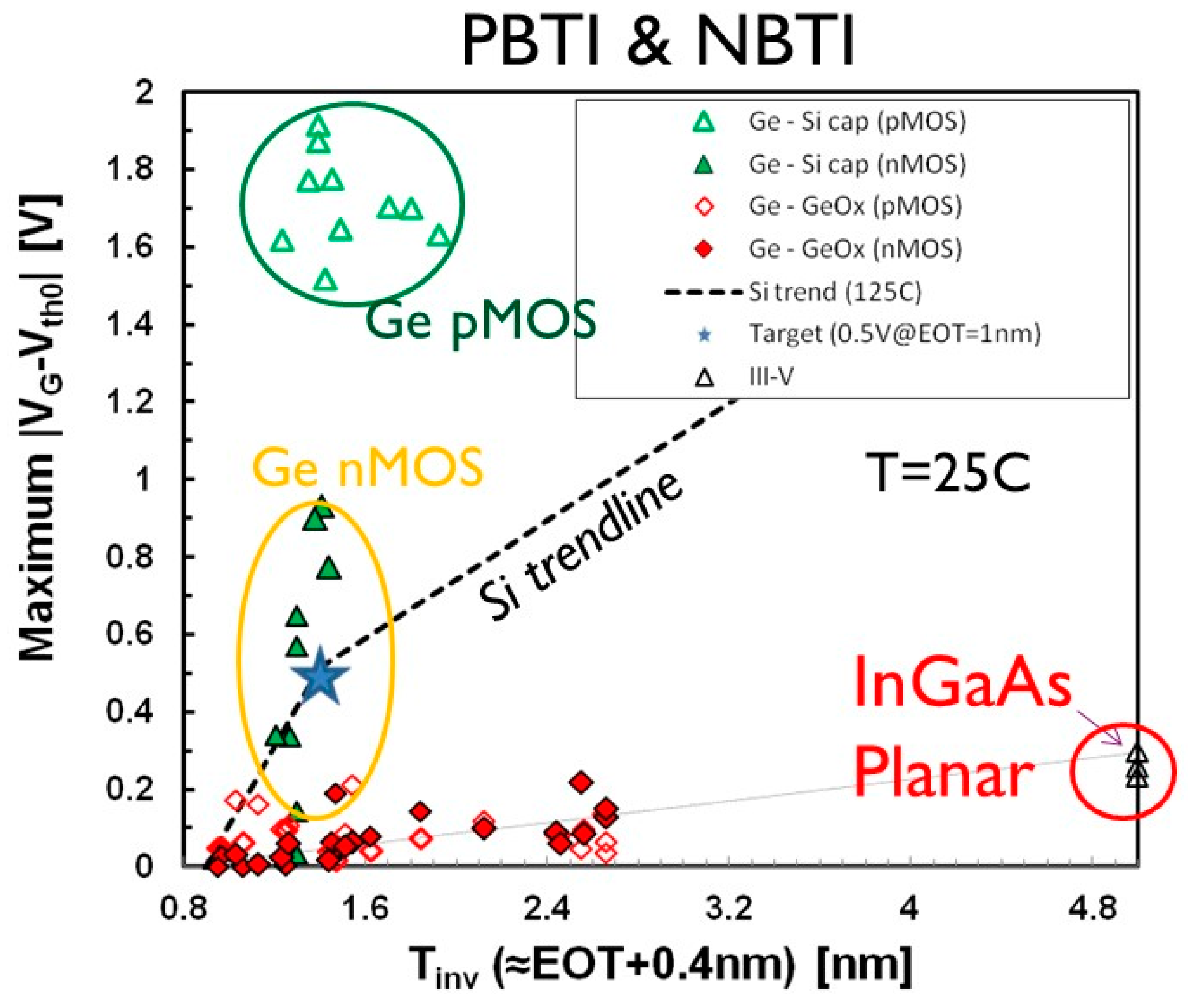
4. Innovations in Gate Stack

Whereas Si has a stable oxide, the passivation of (Si)Ge and III-V is much more complex and the formation of a gate stack with low interface and gate dielectric defects is one of the major challenges for high mobility materials. Reduction of the defects at the interface and in the dielectric is key to improve performance and electrostatic behavior, next to achieving the required reliability performance.
In the case of Ge, the GeO2 interface layer is thermodynamically unstable and the layer decomposes in sub-oxides GeyOx at temperatures higher than 400 °C [21]. Dangling bonds at the interface cannot be H-passivated by typical Si-based forming gas anneals. Although a lot of research has been spent on trying to find a reliable and scalable gate stack, only a few routes are being pursued at this moment for Ge and SiGe channels. The first approach uses the growth of a thin Si cap layer on top of the high mobility material, which is then subsequently partially or fully oxidized [22]. This can be combined with standard high-k materials like HfO2 and the approach is compatible with FinFET topography and can be used on both Ge and SiGe. For SiGe, the pre-clean before Si cap growth is more challenging [15] than in the Ge case. Using this approach, extremely good Bias Temperature Instability (BTI) has been shown [23] for Ge PMOS devices (Figure 2). BTI is responsible for a significant shift in device parameters and as such limits the overall device lifetime, represented by the maximum overdrive voltage. This improvement can be attributed to the fact that only a part or small amount of the oxide traps in the high-κ layer is accessible by the carriers in the channel. The main concern remaining for this gate stack is its scalability: the depleted Si layer contributes to the inversion capacitance, making the Capacitance Equivalent Thickness (CET) or Tinv larger.
The second approach uses plasma oxidation through a thin Al2O3 layer, using Atomic Layer Deposition (ALD). This has been demonstrated for both Ge PMOS and NMOS [24]. The idea behind the approach is that the Al2O3 acts a protecting layer to prevent subsequent damage to the GeOx interface layer and also acts as an oxygen barrier to form ultrathin GeOx layers with high thickness controllability. However, while this seems to be a more scalable approach, the reliability performance of this gate stack has so far not been shown to outperform the Si-cap based gate stack (Figure 2).
The latter approach has also been tried on III-V [25]. While reduction in interface traps and hysteresis has been shown, significant improvements in gate stack performance are needed to show the real potential of III-V [26]. In general, the passivation of the III-V/high-k interface is even more challenging than (Si)Ge as several defect states can be found in the band gap, related to Ga-O, As-O, Ga- or As-dangling bonds. Ga-O and Ga-dangling bonds are responsible for defect states close to the conduction band while As-O and As-dangling bonds are responsible for the states close to the valence band [27]. The midgap states originate from the As and Ga vacancies coming from the surface oxidation itself [28] and are different from the former defects, which cannot be removed by wet chemical treatment or the self-cleaning effect of the ALD deposition of the high-k layer [29]. For InGaAs, a large defect peak is observed close to the valence band edge and a smaller peak exists at mid gap [27]. Both peaks are donor peaks and are uncharged when the Fermi level is close to the conduction band edge. As such, this is beneficial for the on-state but can lead to degradation of the subthreshold swing and higher off-state leakage. Fermi-level pinning by acceptor-like traps in the conduction band, however, severely degrades the on-state performance of the devices.
Next to that, the interaction of the carriers with traps in the gate dielectric can lead to frequency dispersion in both the CV and the MOSFET transconductance curves, leading to hysteresis. The charging of slow traps leads to stress-time dependent threshold voltage shifts and can impact the overall device reliability significantly (Figure 2). J. Franco et al. showed that larger median shifts and aging-induced variance are seen in InGaAs FinFETs w.r.t. their Si counterparts. The latter can be attributed to a larger stochastic impact of single defects on the device characteristics [30], showing that suppressing the defectivity in the channel, at the interface, and in the gate oxide is crucial for the successful introduction of III-V devices.

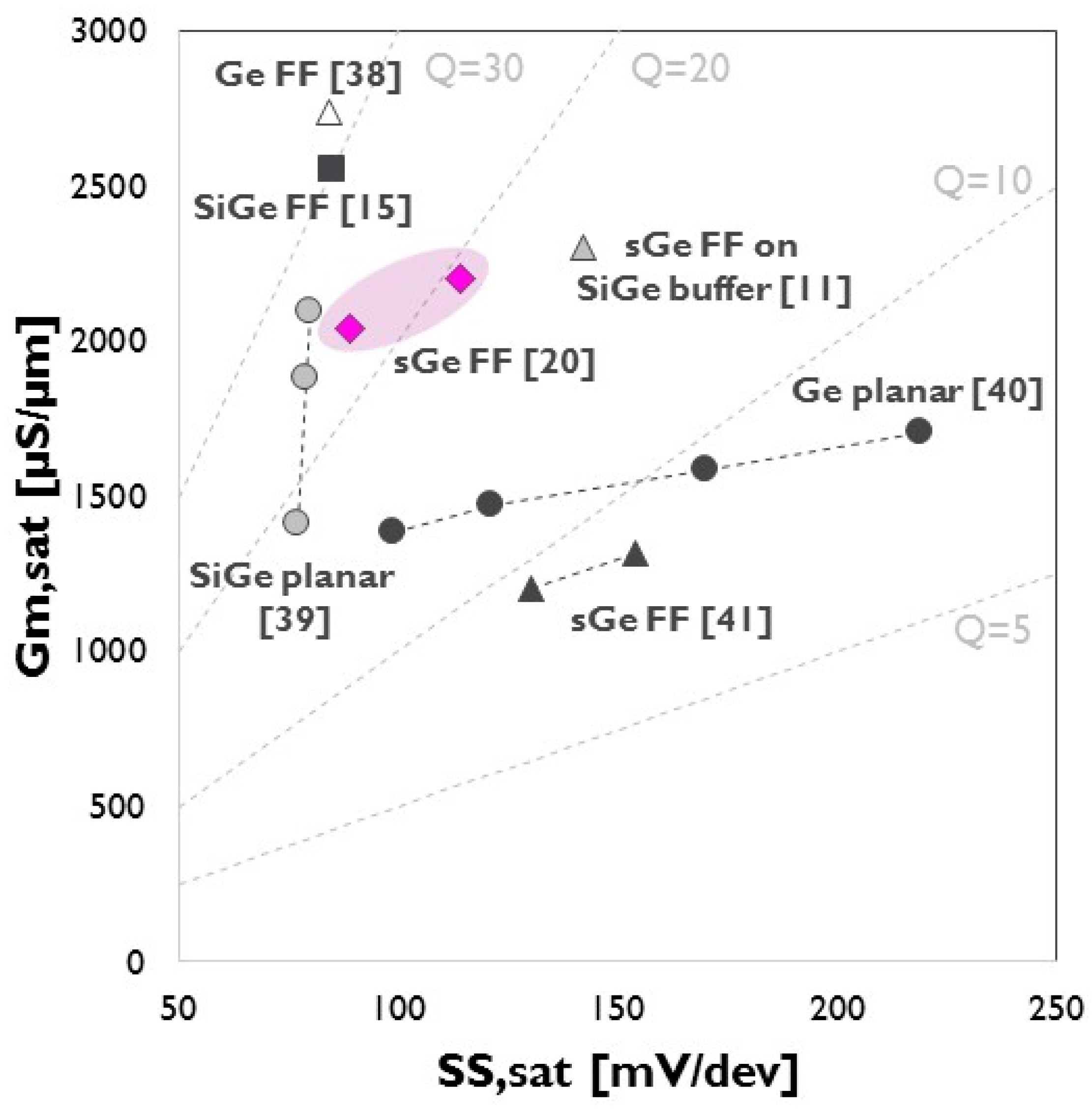
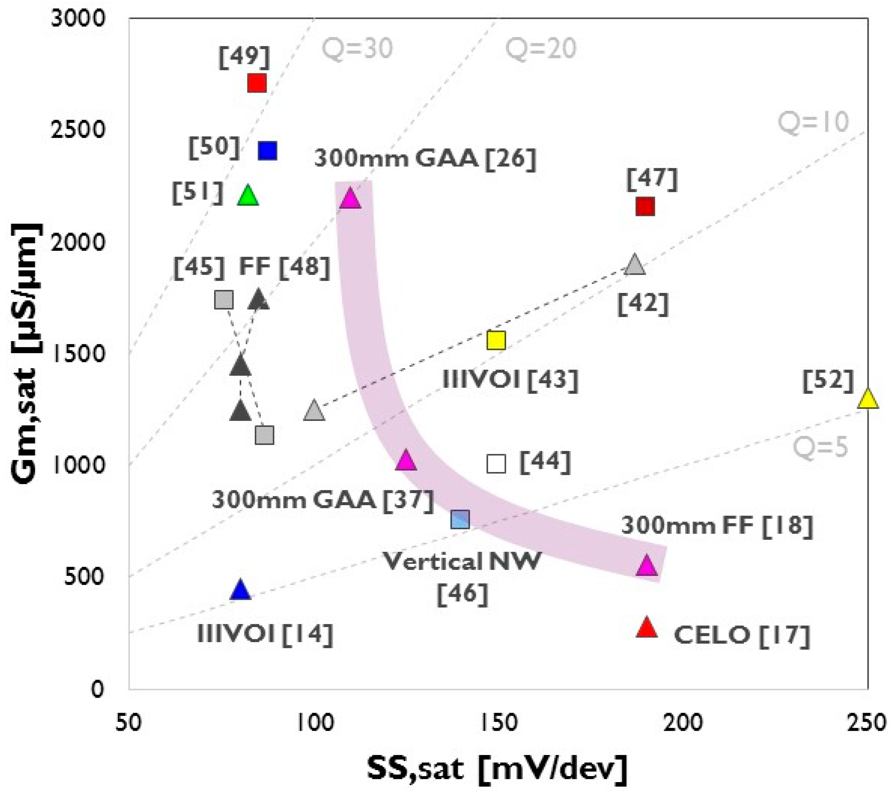
5. Performance of Scaled High Mobility Devices

The overall concern with high mobility materials is their lower bandgap as compared to Si. This reduced bandgap can give rise to an increased off-state leakage, even at lower supply voltage. Next to that, the reduced scalability as compared to Si, gives rise to higher subthreshold leakage for a given gate length and fin width. The main concern is, however, the higher junction leakage and especially the extension leakage. It was already shown that this extension leakage is dominated by the band-to-band tunneling (BTBT) at the extension/channel side, which is intrinsic to the low bandgap of these materials and cannot be impacted by, e.g., reducing the amount of defects [31,32]. Junction engineering and reduction of the supply voltage can help to reduce the electric field at the drain junction. In [31], it is also shown that for supply voltages below 0.7 V, extension leakage currents below 100 nA/μm can be obtained, thereby fulfilling the high performance (HP) targets. LOP (low operating power) and LSTP (low standby power) specifications will require much higher reduction of the electric fields and as a consequence this will limit the drive current significantly. In that respect, SiGe is an interesting material for PMOS [33]: while the hole mobility is not as high as for Ge, up to 85% Ge its bandgap is very Si-like, thereby allowing us to control the BTBT leakage more effectively.
While for future technology nodes the fin width or the nanowire diameter will need to be scaled down well below 10 nm, the increased quantization effects will give rise to an increase of the bandgap which might be beneficial to reduce this BTBT leakage [34,35]. However, this will go at a cost of decreased mobility as was already shown in [36] for III-V channels and trade-off between leakage and performance will be needed.
Finally, Figure 3 and Figure 4 show the maximum saturation transconductance, a measure for mobility, as function of subthreshold swing, measure for short channel behavior, for different (Si)Ge and III-V devices reported in the literature.
Scaled Ge and SiGe PMOS devices with high performance have been shown at reduced supply voltage, demonstrating the clear potential of these alternative materials. In the case of III-V, the highest Q-factors (Q = Gm,sat/SSsat) are found for devices with higher In-content channels showing the benefit of the higher electron mobility, and fabricated on small size InP or Si substrates, using either thick buffer layers or III-V on insulator substrates, indicating the importance of defect control. The subthreshold swing can be kept under control by using either a Quantum Well (QW), FinFET or nanowire structure. However, over the last years, also significant improvement in performance has been shown for the InGaAs/InP FinFET [18] and nanowire devices [26,37], monolithically integrated on 300 mm Si substrates.

6. Towards Functional Scaling

Standard density scaling is going through rough times with increasing difficulties of reducing the metal and gate pitch. Instead of scaling the gates and devices, there is increasing interest in adding more functionalities to the system rather than reducing the overall footprint of the devices. In particular, applications like IoT, new computing technologies and 5G will require the combination of analog/RF, mixed signal, memory, sensors and digital technologies. While this brings along new challenges, novel power-efficient circuits and systems can be designed in this way. Especially in the context of high mobility materials, one can think of the co-integration of III-V and (Si)Ge photonics for off-chip/on-chip optical interconnections and sensors [53] with high mobility CMOS. Arrays of InP lasers monolithically integrated on 300 mm Si have recently been demonstrated [54], essentially using the fin replacement technique to grow the InP layer in V-grooved Si trenches.
Even more interesting is the use of III-V for RF. III-V High Electron Mobility Transistors (HEMT) are already in standard use for high frequency applications where cutoff frequencies exceeding 1THz [55] have been demonstrated. The RF performance of these devices significantly outperforms that of standard CMOS devices, especially when considering FinFET which suffers from intrinsically higher parasitics. Next to that, III-V and (Si)Ge heterojunction bipolar transistors (HBT) have also shown great potential when high speed requirements need to be fulfilled [56].
So far, Si and III-V circuits have always been fabricated and packaged separately, and then later assembled on the same carrier substrate, which does not really allow the optimization of performance, reduction of power, cost and form factor, and increase in the complexity of the circuit [57]. Circuits that could benefit from a Si/III-V hybrid approach are power amplifiers (PA) [58], low noise amplifiers (LNA) and voltage controlled oscillators (VCO).
Different integration schemes can be considered: apart from the co-integration in the same plane, 3D monolithic integration is being considered where the III-V devices are built on top of the Si CMOS [59]. As the III-V processing requires much reduced temperatures, these are perfect materials to process on top of Si CMOS.

7. Conclusions

For the 7 nm technology node and beyond, high mobility materials like (Si)Ge and III-V are being considered for high performance devices at reduced supply voltage. While high electron and hole mobilities can be achieved using these materials, surface passivation, the design of a reliable and scalable gate stack and the fabrication of substrates with low defectivity are still the major challenges for this technology where both wide bandgap materials and low bandgap high mobility materials need to be co-integrated on the same wafer.
Beyond the standard density scaling, these materials will play a key role in enhancing the functionality of future electronic systems, allowing the co-integration of Si CMOS with specialized components like III-V HEMT or HBT.

Acknowledgments

This work is supported by the imec (sub-)10-nm IIAP program members and the European Community’s Seventh Framework Program (FP7/2007-2013) under Grant Agreement III-V-MOS Project No. 619326. Finally, the author would also like to acknowledge the outstanding contributions of the Ge and III-V research teams.

Conflicts of Interest

The author declares no conflict of interest.

References

  1. Eryilmaz, S.B.; Kuzum, D.; Yu, S.; Wong, H.S.P. Device and System Level Design Considerations for Analog-Non-Volatile-Memory Based Neuromorphic Architectures. In Proceedings of the 2015 IEEE International Electron Devices Meeting, Washington, DC, USA, 7–9 December 2015; pp. 64–67.
  2. Simmons, M.Y. Quantum computing in Silicon. In Proceedings of the 2015 IEEE International Electron Devices Meeting, Washington, DC, USA, 7–9 December 2015; pp. 6–9.
  3. Steegen, A. Technology innovation in an IoT Era. In Proceedings of the 2015 Symposium on VLSI Circuits, Kyoto, Japan, 17–19 June 2015; pp. C170–C171.
  4. Golikova, O.A.; Moizhez, B.Y.; Stilbans, L.S. Hole mobility of germanium as a function of concentration and temperature. Sov. Phys. Solid State 1962, 3, 2259–2265. [Google Scholar]
  5. Rode, D.L. Semiconductors and Semimetals; Willardson, R.K., Beer, A.C., Eds.; Academic Press: Cambridge, MA, USA, 1975; Volome 10, p. 1. [Google Scholar]
  6. Magnone, P.; Crupi, F.; Alioto, M.; Kaczer, B.; de Jaeger, B. Understanding the Potential and the Limits of Germanium pMOSFETs for VLSI Circuits from Experimental Measurements. IEEE Trans. VLSI Syst. 2011, 19, 1569–1582. [Google Scholar] [CrossRef]
  7. Ghosh, S.; Leonhardt, D.; Han, S.M. Effect of threading dislocation density and dielectric layer on temperature-dependent electrical characteristics of high-hole-mobility metal semiconductor field effect transistors fabricated from wafer-scale epitaxially grown p-type germanium on silicon substrates. J. Appl. Phys. 2014, 115, 094507. [Google Scholar]
  8. Koslowski, G.; Fursenko, O.; Zaumseil, P.; Schroeder, T.; Vorderwestner, M.; Storck, P. The epitaxial growth of low defect SiGe buffer layers for integration of new materials on 300 mm silicon wafers. ECS Trans. 2012, 50, 613–621. [Google Scholar] [CrossRef]
  9. Huang, M.L.; Chang, S.W.; Chen, M.K.; Fan, C.H.; Lin, H.T.; Lin, C.H.; Chu, R.L.; Lee, K.Y.; Khaderbad, M.A.; Chen, Z.C.; et al. In0.53Ga0.47As MOSFETs with high channel mobility and gate stack quality fabricated on 300 mm Si substrate. In Proceedings of the 2015 Symposium on VLSI Technology (VLSI Technology), Kyoto, Japan, 16–18 June 2015; p. T205.
  10. Goh, K.H.; Tan, K.H.; Yadav, S.; Yoon, S.F.; Liang, G.; Gong, X.; Yeo, Y.C. Gate-All-Around CMOS (InAs n-FET and GaSb p-FET) based on Vertically-Stacked Nanowires on a Si Platform, Enabled by Extremely-Thin Buffer Layer Technology and Common Gate Stack and Contact Modules. In Proceedings of the 2015 IEEE International Electron Devices Meeting, Washington, DC, USA, 7–9 December 2015; pp. 394–397.
  11. Mitard, J.; Witters, L.; Loo, R.; Lee, S.H.; Sun, J.W.; Franco, J.; Ragnarsson, L.Å.; Brand, A.; Lu, X.; Yoshida, N.; et al. 15 nm-WFIN high-performance low-defectivity strained-germanium pFinFETs with low temperature STI-last process. In Proceedings of the 2014 Symposium on VLSI Technology (VLSI-Technology): Digest of Technical Papers, Honolulu, HI, USA, 9–12 June 2014; pp. 1–2.
  12. Bury, E.; Kaczer, B.; Mitard, J.; Collaert, N.; Khatami, N.S.; Aksamija, Z.; Vasileska, D.; Raleva, K.; Witters, L.; Hellings, G.; et al. Characterization of Self-Heating in High-Mobility Ge FinFET pMOS devices. In Proceedings of the 2015 Symposium on VLSI Technology (VLSI Technology), Kyoto, Japan, 16–18 June 2015; p. T60.
  13. Nakaharai, S.; Tezuka, T.; Sugiyama, N.; Moriyama, Y.; Takagi, S. Characterization of 7-nm-thick strained Ge-on-insulator layer fabricated by Ge-condensation technique. Appl. Phys. Lett. 2003, 83, 3516–3518. [Google Scholar] [CrossRef]
  14. Djara, V.; Deshpande, V.; Uccelli, E.; Daix, N.; Caimi, D.; Rossel, C.; Sousa, M.; Siegwart, H.; Marchiori, C.; Hartmann, J.M.; et al. An InGaAs on Si Platform for CMOS with 200 mm InGaAs-OI Substrate, Gate-first, Replacement Gate Planar and FinFETs Down to 120 nm Contact Pitch. In Proceedings of the 2015 Symposium on VLSI Technology (VLSI Technology), Kyoto, Japan, 16–18 June 2015; pp. T176–T177.
  15. Hashemi, P.; Balakrishnan, K.; Engelmann, S.U.; Ott, J.A.; Khakifirooz, A.; Baraskar, A.; Hopstaken, M.; Newbury, J.S.; Chan, K.K.; Leobandung, E.; Mo, R.T.; et al. First demonstration of high-Ge-content strained-Si1-xGex (x = 0.5) on insulator PMOS FinFETs with high hole mobility and aggressively scaled fin dimensions and gate lengths for high-performance applications. In Proceedings of the 2014 IEEE International Electron Devices Meeting, San Francisco, CA, USA, 15–17 December 2014; pp. 16.1.1–16.1.4.
  16. Yokoyama, M.; Kim, S.H.; Zhang, R.; Taoka, N.; Urabe, Y.; Maeda, T.; Takagi, H.; Yasuda, T.; Yamada, H.; Ichikawa, O.; et al. CMOS integration of InGaAs nMOSFETs and Ge pMOSFETs with self-align Ni-based metal S/D using direct wafer bonding. In Proceedings of the 2011 Symposium on VLSI Technology (VLSIT), Honolulu, HI, USA, 14–16 June 2011; pp. 60–61.
  17. Czornomaz, L.; Uccelli, E.; Sousa, M.; Deshpande, V.; Djara, V.; Caimi, D.; Rossell, M.D.; Erni, R.; Fompeyrine, J. Confined Epitaxial Lateral Overgrowth (CELO): A Novel Concept for Scalable Integration of CMOS-compatible InGaAs-on-insulator MOSFETs on Large-Area Si Substrates. In Proceedings of the 2015 Symposium on VLSI Technology (VLSI Technology), Kyoto, Japan, 16–18 June 2015; pp. T172–T173.
  18. Waldron, N.; Merckling, C.; Guo, W.; Ong, P.; Teugels, L.; Ansar, S.; Tsvetanova, D.; Sebaai, F.; van Dorp, D.H.; Milenin, A.; et al. An InGaAs/InP Quantum Well FinFet Using the Replacement Fin Process Integrated in an RMG Flow on 300 mm Si Substrates. In Proceedings of the 2014 Symposium on VLSI Technology (VLSI-Technology): Digest of Technical Papers, Honolulu, HI, USA, 9–12 June 2014; pp. 1–2.
  19. Merckling, C.; Waldron, N.; Jiang, S.; Guo, W.; Ryan, P.; Collaert, N.; Caymax, M.; Barla, K.; Heyns, M.; Thean, A.; et al. Selective-Area Metal Organic Vapor-Phase Epitaxy of InGaAs/InP Heterostrucures on Si For Advanced CMOS Devices. ECS Trans. 2014, 61, 107–112. [Google Scholar] [CrossRef]
  20. Witters, L.; Mitard, J.; Loo, R.; Demuynck, S.; Chew, S.A.; Schram, T.; Tao, Z.; Hikavyy, A.; Sun, J.W.; Milenin, A.P.; et al. Strained germanium quantum well p-finFETs fabricated on 45 nm fin pitch using replacement channel, replacement metal gate and germanide-free local interconnect. In Proceedings of the 2015 Symposium on VLSI Technology (VLSI Technology), Kyoto, Japan, 16–18 June 2015; pp. T56–T57.
  21. Kita, K.; Suzuki, S.; Nomura, H.; Takahashi, T.; Nishimura, T.; Toriumi, A. Direct Evidence of GeO Volatilization from GeO2/Ge and Impact of Its Suppression on GeO2/Ge Metal-Insulator-Semiconductor Characteristics. Jpn. J. Appl. Phys. 2008, 47, 2349. [Google Scholar] [CrossRef]
  22. Leys, F.E.; Bonzom, R.; Kaczer, B.; Janssens, T.; Vandervorst, W.; De Jaeger, B.; Van Steenbergen, J.; Martens, K.; Hellin, D.; Rip, J.; et al. Thin epitaxial Si films as a passivation method for Ge(001): Influence of deposition temperature on Ge surface segregation and the high-k/Ge interface quality. Mater. Sci. Semicond. Process. 2006, 9, 679–684. [Google Scholar] [CrossRef]
  23. Groeseneken, G.; Franco, J.; Cho, M.; Kaczer, B.; Toledano-Luque, M.; Roussel, Ph.; Kauerauf, T.; Alian, A.; Mitard, J.; Arimura, H.; et al. BTI reliability of advanced gate stacks for Beyond-Silicon devices: Challenges and opportunities. In Proceedings of the 2014 IEEE International Electron Devices Meeting, San Francisco, CA, USA, 15–17 December 2014; pp. 34.4.1–34.4.4.
  24. Zhang, R.; Taoka, N.; Huang, P.C.; Takenaka, M.; Takagi, S. 1-nm-thick EOT High Mobility Ge n- and p-MOSFETs with Ultrathin GeOx/Ge MOS Interfaces Fabricated by Plasma Post Oxidation. In Proceedings of the 2011 IEEE International Electron Devices Meeting, Washington, DC, USA, 5–7 December 2011; pp. 642–645.
  25. Sun, Y.; Kiewra, E.W.; de Souza, J.P.; Bucchignano, J.J.; Fogel, K.E.; Sadana, D.K.; Shahidi, G.G. High-Performance In0.7Ga0.3As-Channel MOSFETs with High-κ Gate Dielectrics and α-Si Passivation. IEEE Electron. Device Lett. 2009, 30, 5–7. [Google Scholar] [CrossRef]
  26. Waldron, N.; Sioncke, S.; Franco, J.; Nyns, L.; Vais, A.; Zhou, X.; Lin, H.C.; Boccardi, G.; Maes, J.W.; Xie, Q.; et al. Gate-All-Around InGaAs Nanowire FETs with Peak Transconductance of 2200µA/µm at 50 nm Lg using a Replacement Fin RMG Flow. In Proceedings of the 2015 IEEE International Electron Devices Meeting, Washington, DC, USA, 7–9 December 2015; pp. 799–802.
  27. Brammertz, G.; Lin, H.C.; Martens, K.; Alian, A.; Merckling, C.; Penaud, J.; Kohen, D.; Wang, W.E.; Sioncke, S.; Delabie, A.; et al. Electronic properties of III-V/oxide interfaces. ECS Trans. 2009, 19, 375–386. [Google Scholar]
  28. Scarrozza, M.; Pourtois, G.; Houssa, M.; Caymax, M.; Stesmans, A.; Meuris, M.; Heyns, M.M. A first-principles study of the structural and electronic properties of III-V/thermal oxide interfaces. Microelectron. Eng. 2009, 86, 1747–1750. [Google Scholar] [CrossRef]
  29. Ye, P.D.; Wilk, G.D.; Kwo, J.; Yang, B.; Gossmann, H.J.L.; Frei, M.; Chu, S.N.G.; Mannaerts, J.P.; Sergent, M.; Hong, M.; Ng, K.K.; Bude, J. GaAs MOSFET with oxide gate dielectric grown by atomic layer deposition. IEEE Electron. Device Lett. 2003, 24, 209–211. [Google Scholar] [CrossRef]
  30. Franco, J.; Kaczer, B.; Waldron, N.; Roussel, Ph.J.; Alian, A.; Pourghaderi, M.A.; Ji, Z.; Grasser, T.; Kauerauf, T.; Sioncke, S.; Collaert, N.; Thean, A.; Groeseneken, G. RTN and PBTI-induced Time-Dependent Variability of Replacement Metal-Gate High-k InGaAs FinFETs. In Proceedings of the 2014 IEEE International Electron Devices Meeting, San Francisco, CA, USA, 15–17 December 2014; pp. 506–509.
  31. Eneman, G.; De Jaeger, B.; Simoen, E.; Brunco, D.P.; Hellings, G.; Mitard, J.; De Meyer, K.; Meuris, M.; Heyns, M. Quantification of Drain Extension Leakage in a Scaled Bulk Germanium PMOS Technology. IEEE Trans. Electron. Devices 2009, 56, 3115–3121. [Google Scholar] [CrossRef]
  32. Lin, J.; Zhao, X.; Antoniadis, D.A.; del Alamo, J.A. A New Self-aligned Quantum-Well MOSFET Architecture Fabricated by a Scalable Tight-Pitch Process. In Proceedings of the 2013 IEEE International Electron Devices Meeting, Washington, DC, USA, 9–11 December 2013; pp. 421–424.
  33. Crupi, F.; Alioto, M.; Franco, J.; Magnone, P.; Kaczer, B.; Groeseneken, G.; Mitard, J.; Witters, L.; Hoffmann, T.Y. Buried Silicon-Germanium pMOSFETs: Experimental Analysis in VLSI Circuits under Aggressive Voltage Scaling. IEEE Trans. VLSI Syst. 2012, 20, 1487–1495. [Google Scholar] [CrossRef]
  34. Krishnamohan, T.; Kim, D.; Nguyen, C.D.; Jungemann, C.; Nishi, Y.; Saraswat, K.C. High-mobility low band-to-band-tunneling strained-Germanium double-gate heterostructure FETs: Simulations. IEEE Trans. Electron. Devices 2006, 53, 1000–1009. [Google Scholar] [CrossRef]
  35. Zerveas, G.; Caruso, E.; Baccarani, G.; Czornomaz, L.; Daix, N.; Esseni, D.; Gnani, E.; Gnudi, A.; Grassi, R.; Luisier, M.; et al. Comprehensive comparison and experimental validation of band-structure calculation methods in III-V semiconductor quantum wells. Solid-State Electron. 2016, 115 Pt B, 92–102. [Google Scholar] [CrossRef] [Green Version]
  36. Alian, A.; Pourghaderi, M.A.; Mols, Y.; Cantoro, M.; Ivanov, T.; Collaert, N.; Thean, A. Impact of the channel thickness on the performance of ultrathin InGaAs channel MOSFET devices. In Proceedings of the 2013 IEEE International Electron Devices Meeting, Washington, DC, USA, 9–11 December 2013; pp. 16.6.1–16.6.4.
  37. Waldron, N.; Merckling, C.; Teugels, L.; Ong, P.; Ibrahim, S.A.U.; Sebaai, F.; Pourghaderi, A.; Barla, K.; Collaert, N.; Thean, A.V.Y. InGaAs Gate-All-Around Nanowire Devices on 300 mm Si Substrates. IEEE Electron. Device Lett. 2014, 35, 1097–1099. [Google Scholar] [CrossRef]
  38. Duriez, B.; Vellianitis, G.; van Dal, M.J.H.; Doornbos, G.; Oxland, R.; Bhuwalka, K.K.; Holland, M.; Chang, Y.S.; Hsieh, C.H.; Yin, K.M.; et al. Scaled p-channel Ge FinFET with optimized gate stack and record performance integrated on 300 mm Si wafers. In Proceedings of the 2013 IEEE International Electron Devices Meeting, Washington, DC, USA, 9–11 December 2013; pp. 522–525.
  39. Mitard, J.; Witters, L.; Eneman, G.; Hellings, G.; Pantisano, L.; Hikavyy, A.; Loo, R.; Eyben, P.; Horiguchi, N.; Thean, A. 85 nm-Wide 1.5mA/μm-ION IFQW SiGe-pFET: Raised vs. Embedded Si0.75Ge0.25 S/D Benchmarking and in-Depth Hole Transport Study. In Proceedings of the 2012 Symposium on VLSI Technology (VLSIT), Honolulu, HI, USA, 12–14 June 2012; pp. 163–164.
  40. Pillarisetty, R.; Chu-Kung, B.; Corcoran, S.; Dewey, G.; Kavalieros, J.; Kennel, H.; Kotlyar, R.; Le, V.; Lionberger, D.; Metz, M.; et al. High Mobility Strained Germanium Quantum Well Field Effect Transistor as the P-Channel Device Option for Low Power (Vcc = 0.5 V) III–V CMOS Architecture. In Proceedings of the 2010 IEEE International Electron Devices Meeting, San Francisco, CA, USA, 6–8 December 2010; pp. 6.7.1–6.7.4.
  41. Witters, L.; Mitard, J.; Loo, R.; Eneman, G.; Mertens, H.; Brunco, D.P.; Lee, S.H.; Waldron, N.; Hikavyy, A.; Favia, P.; et al. Strained Germanium Quantum Well pMOS FinFETs Fabricated on in situ Phosphorus-Doped SiGe Strain Relaxed Buffer Layers Using a Replacement Fin Process. In Proceedings of the 2013 IEEE International Electron Devices Meeting, Washington, DC, USA, 9–11 December 2013; pp. 534–537.
  42. Egard, M.; Ohlsson, L.; Borg, B.M.; Lenrick, F.; Wallenberg, R.; Wernersson, L.E.; Lind, E. High Transconductance Self-Aligned Gate-Last Surface Channel In0.53Ga0.47As MOSFET. In Proceedings of the 2011 IEEE International Electron Devices Meeting, Washington, DC, USA, 5–7 December 2011; pp. 303–306.
  43. Ko, H.; Takei, K.; Kapadia, R.; Chuang, S.; Fang, H.; Leu, P.W.; Ganapathi, K.; Plis, E.; Kim, H.S.; Chen, S.Y.; et al. Ultrathin compound semiconductor on insulator layers for high-performance nanoscale transistors. Nature 2010, 468, 286–289. [Google Scholar] [CrossRef] [PubMed]
  44. Hill, R.; Park, C.; Barnett, J.; Price, J.; Huang, J.; Goel, N.; Loh, W.Y.; Oh, J.; Smith, C.E.; Kirsch, P.; Majhi, P.; Jammy, R. Self-aligned III-V MOSFETs heterointegrated on a 200 mm Si substrate using an industry standard process flow. In Proceedings of the 2010 IEEE International Electron Devices Meeting, San Francisco, CA, USA, 6–8 December 2010; pp. 6.2.1–6.2.4.
  45. Thathachar, A.V.; Agrawal, N.; Bhuwalka, K.K.; Cantoro, M.; Heo, Y.C.; Lavallee, G.; Maeda, S.; Datta, S. Indium Arsenide (InAs) Single and Dual Quantum-Well Heterostructure FinFETs. In Proceedings of the 2015 Symposium on VLSI Technology (VLSI Technology), Kyoto, Japan, 16–18 June 2015; pp. T208–T209.
  46. Thelander, C.; Froberg, L.E.; Rehnstedt, C.; Samuelson, L.; Wernersson, L.E. Vertical enhancement-mode InAs nanowire field-effect transistor with 50-nm wrap gate. IEEE Electron Device Lett. 2008, 29, 206–208. [Google Scholar] [CrossRef]
  47. Lee, S.; Huang, C.Y.; Carter, A.D.; Elias, D.C.; Law, J.J.M.; Chobpattana, V.; Krämer, S.; Thibeault, B.J.; Mitchell, W.; Stemmer, S.; et al. Record Extrinsic Transconductance (2.45 mS/μm at VDS = 0.5 V) InAs/In0.53Ga0.47As Channel MOSFETs Using MOCVD Source-Drain Regrowth. In Proceedings of the 2015 Symposium on VLSI Technology (VLSIT), Kyoto, Japan, 11–13 June 2013; p. T247.
  48. Radosavljevic, M.; Chu-Kung, B.; Corcoran, S.; Dewey, G.; Hudait, M.K.; Fastenau, J.M.; Kavalieros, J.; Liu, W.K.; Lubyshev, D.; Metz, M.; et al. Advanced High-K Gate Dielectric for High-Performance Short-Channel In0.7Ga0.3As Quantum Well Field Effect Transistors on Silicon Substrate for Low Power Logic Applications. In Proceedings of the 2009 IEEE International Electron Devices Meeting (IEDM), Baltimore, MD, USA, 7–9 December 2009; pp. 319–322.
  49. Chang, S.W.; Li, X.; Oxland, R.; Wang, S.W.; Wang, C.H.; Contreras-Guerrero, R.; Bhuwalka, K.K.; Doornbos, G.; Vasen, T.; Holland, M.C.; et al. InAs N-MOSFETs with record performance of Ion = 600 μA/μm at Ioff = 100 nA/mm (Vd = 0.5 V). In Proceedings of the 2013 IEEE International Electron Devices Meeting, Washington, DC, USA, 9–11 December 2013; pp. 417–420.
  50. Lee, S.; Chobpattana, V.; Huang, C.-Y.; Thibeault, B.J.; Mitchell, W.; Stemmer, S.; Gossard, A.C.; Rodwell, M.J.W. Record Ion (0.50 mA/μm at VDD = 0.5 V and Ioff = 100 nA/μm) 25 nm-Gate-Length ZrO2/InAs/InAlAs MOSFETs. VLSI Technol. In Proceedings of the 2014 Symposium on VLSI Technology (VLSI-Technology): Digest of Technical Papers, Honolulu, HI, USA, 9–12 June 2014; pp. 64–65.
  51. Zhou, X.; Alian, A.; Mols, Y.; Rooyackers, R.; Eneman, G.; Lin, D.; Ivanov, T.; Pourghaderi, A.; Collaert, N.; Thean, A. In0.53Ga0.47As quantum-well MOSFET with source/drain regrowth for low power logic applications. In Proceedings of the 2014 Symposium on VLSI Technology (VLSI-Technology): Digest of Technical Papers, Honolulu, HI, USA, 9–12 June 2014; pp. 1–2.
  52. Wu, Y.Q.; Wang, R.S.; Shen, T.; Gu, J.J.; Ye, P.D. First Experimental Demonstration of 100 nm Inversion-mode InGaAs FinFET through Damage-free Sidewall Etching. In Proceedings of the 2009 IEEE International Electron Devices Meeting (IEDM), Baltimore, MD, USA, 7–9 December 2009; pp. 331–334.
  53. Takenaka, M.; Kim, Y.; Han, J.; Kang, J.; Ikku, Y.; Cheng, Y.; Park, J.K.; Kim, S.H.; Takagi, S. CMOS photonics technologies based on heterogeneous integration of SiGe/Ge and III-V on Si. In Proceedings of the 2015 IEEE International Electron Devices Meeting, Washington, DC, USA, 7–9 December 2015; pp. 815–818.
  54. Wang, Z.; Tian, B.; Pantouvaki, M.; Guo, W.; Absil, P.; Van Campenhout, J.; Merckling, C.; Van Thourhout, D. Room-temperature InP distributed feedback laser array directly grown on silicon. Nat. Photonics 2015, 9, 837–842. [Google Scholar] [CrossRef]
  55. Kim, D.H.; del Alamo, J.A.; Chen, P.; Ha, W.; Urteaga, M.; Brar, B. 50-nm E-mode In0.7Ga0.3As PHEMTs on 100-mm InP substrate with fmax > 1 THz. In Proceedings of the 2010 IEEE International Electron Devices Meeting, San Francisco, CA, USA, 6–8 December 2010; pp. 692–695.
  56. Ida, M.; Kurishima, K.; Watanabe, N. Over 300 GHz f/sub T/ and f/sub max/ InP/InGaAs double heterojunction bipolar transistors with a thin pseudomorphic base. IEEE Electron. Device Lett. 2002, 23, 694–696. [Google Scholar] [CrossRef]
  57. Hoke, W.E.; Chelakara, R.V.; Bettencourt, J.P.; Kazior, T.E.; LaRoche, J.R.; Kennedy, T.D.; Mosca, J.J.; Torabi, A.; Kerr, A.J.; Lee, H.S.; et al. Monolithic integration of silicon CMOS and GaN transistors in a current mirror circuit. J. Vac. Sci. Technol. B 2012, 30, 02B101. [Google Scholar] [CrossRef]
  58. Ge, T.; Guo, L.; He, H.; Yang, K.; Jia, Y.; Chang, J. Envelope Tracking RF Power Amplifiers: Fundamentals, Design Challenges, and Unique Opportunities Offered by LEES-SMART InGaAs-on-CMOS Process. Procedia Eng. 2016, 141, 94–97. [Google Scholar] [CrossRef]
  59. Desphande, V.; Djara, V.; O’Connor, E.; Caimi, D.; Sousa, M.; Czornomaz, L.; Fompeyrine, J.; Hashemi, P.; Balakrishnan, K. First RF Characterization of InGaAs Replacement Metal Gate (RMG) nFETs on SiGe-OI FinFETs Fabricated by 3D Monolithic Integration. In Proceedings of the EUROSOI/ULIS Conference, Vienna, Austria, 25–27 January 2016; pp. 127–130.
Figure 1. Schematic presentation of the fin replacement process; in this case demonstrated for the channel formation of InGaAs FinFETs.
Jlpea 06 00009 g001
Figure 2. Benchmark plot of maximum overdrive for advanced CMOS technologies. This maximum overdrive represents the maximum overdrive voltage |VGS-VT|, which is allowed to ensure 10 years of reliable continuous operation. Si-passivation of Ge channels yields extremely good reliability for PMOS and is also beneficial for NMOS. GeOx-based gate stacks, however, show much degraded reliability performance, similar to the InGaAs case using Al2O3 as gate dielectric, directly on the III-V channel.
Jlpea 06 00009 g002
Figure 3. Peak extrinsic transconductance as a function of subthreshold swing measured at VDS = −0.5 V comparing different (Si)Ge devices, both planar and FinFET (FF), reported in the literature [11,15,20,38,39,40,41].
Jlpea 06 00009 g003
Figure 4. Peak extrinsic transconductance as function of subthreshold swing measured at VDS = 0.5 V comparing different InGaAs (triangles) and InAs (rectangles) devices reported in the literature; FF = FinFET, GAA = Gate-All-Around and NW = nanowire [14,17,18,42,43,44,45,46,47,48,49,50,51,52].
Jlpea 06 00009 g004

