1. Introduction
The general power consumption equation can be divided into three parts: dynamic, static, and leakage power consumption, which is represented as follows: Ptotal = ItotalVdd = Pdynamic + Pstatic + Pleakage. The first part, Pdynamic = IavgVdd = CloadVdd2FCK, represents dynamic power consumption, where Iavg is the average current consumption, Cload is the circuit output loading, Vdd is the supply voltage, and FCK is the circuit working clock frequency. The second part is the static power consumption of Pstatic = IpeakVdd = TSCIpeakVddFCK, where TSC is the short current duration time, and Ipeak is the peak current during circuit transition time. The Pleakage is the leakage power consumption that includes the leakage current of Ileakage and Vdd.
From the equation Pdynamic = IavgVdd = CloadVdd2FCK, it can be seen that the chip’s power consumption is directly related to supply voltage (Vdd), the chip’s work frequency (FCK), and the chip’s load (Cload). The chip power consumption is directly related to the average current. Hence, the measurement current value (Iavg) will increase when accelerating the working frequency or increasing the supply voltage to the chip.
The Ipeak of a gate is dependent on two factors. The first factor is the input signal transition time. For the same output loading, the input signal with a large transition time (fast signal transition) results in a lower Ipeak. The second factor is that, for two signals with the same transition time, the circuit with the large output loading has a smaller Ipeak than the one with the small output loading. Most of the Iavg comes from the working frequency and the loading of the circuit.
The Ipeak and Iavg values can then be used as the tightened current bounds during the circuit testing phase. If the test circuit is functioning, the current consumption is over the setting bound and the voltage drop increases the circuit delay, which results in test circuit performance degradation. Accordingly, the upper bound is set for the test chip working at a target clock frequency, and the good chip outputs should all be functionally correct. By applying the lower bound to set a power supply current bound under the original design target clock frequency, the test chip output responses should be mostly incorrect. If the test clock frequency is degraded in this situation, there should be fewer incorrect output responses. The functions of the failed chip can then be quickly found by applying this screening technique.
This paper focuses on Ipeak and Iavg issues. This leakage issue is outside the scope of this discussion. The supply voltage (Vdd) and clock frequency (FCK) are not altered in the following discussion. As the Vdd and FCK are not altered, the Ipeak and Iavg current consumptions are not correlated with the supply voltage or clock frequency.
Using the Iavg and Ipeak to quickly detect faulty chips is a comparatively new idea. However, previous research has focused on discussing the testing impact without upper or lower current bounds to screen for faulty chips or use them as components in a statistical outlier analysis.
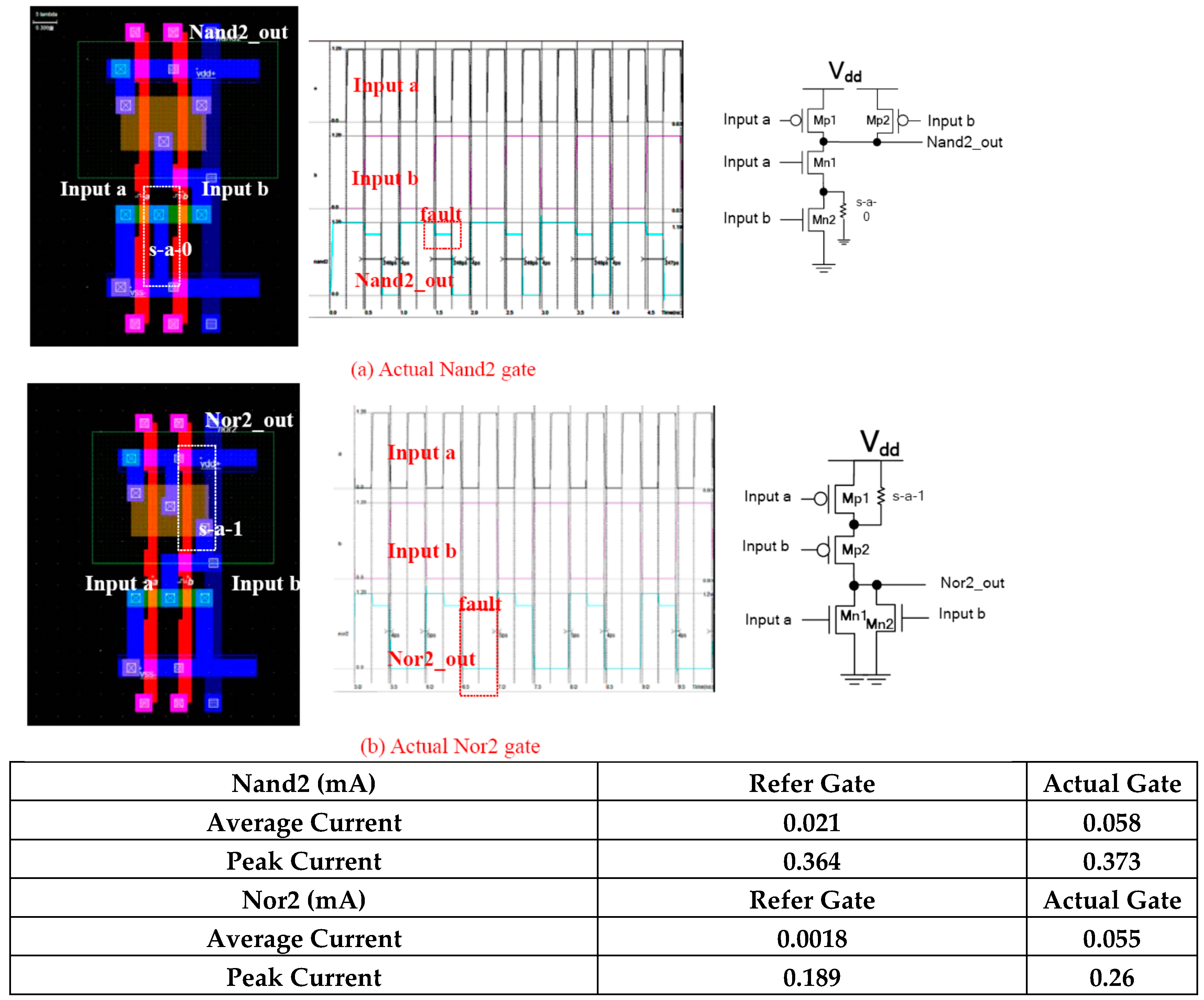
For example, to apply a stuck-fault in a generic CMOS logic gate,
Figure 1a shows a NAND gate with an NMOS transistor connection stuck-on-Vss (s-a-0). The referenced gate functions are without an obvious failure phenomenon. However, there is a nearly three times larger than average current consumption.
Figure 1b shows a NOR gate with a PMOS transistor connection stuck-on-Vdd (s-a-1). This referenced gate has failure functions, and there is a 30-fold larger than average current. The above simulations are based on 0.12-µm technology provided by Microwind [
1]. Although the SPICE-level simulation is in fact accurate, such simulations are not feasible for a large digital circuit.
The above simulations are used to demonstrate the motivation for this current research. Whenever some logic gates fail, they cannot operate and do not consume a normal current in faulty situations. As the above gate demonstrates in the simulation results, all of the functional logic gates in the circuit are activated simultaneously. Hence, the Iavg and Ipeak values are large. There is either a small or large amount of current consumption in abnormal functions. Hence, judging from the Iavg and Ipeak current value comparisons, the good and faulty chips can be detected.
For industry designed chips, faulty chips have abnormal (too large or small) current consumptions in comparison with good chips.
Table 1 shows an example of a large test chip evaluation. From the I
avg and I
peak values, the faulty and good chips show significant differences.
Defective chips exhibit abnormal currents, possibly due to failed or unrealizable designed circuits. This means that, for most normally tested chips, Ipeak and Iavg values are within the designed emulation bounds. Hence, using the designed chip’s emulated Iavg and Ipeak, functionally failed chips can be screened quickly.
It is difficult to accurately measure the Iavg and Ipeak in real time. Hence, there are two monitoring approaches that can be used after setting the limitation of maximum supplied current for the test chip. The first approach entails the monitoring of voltage variance, and the second entails the monitoring of the circuit delay time or functionalities of the circuit under testing.
The voltage drop level can be used to determine whether the designed chip’s consuming current is over the threshold during normal work status. This situation also occurs when the consumed current exceeds the power-rails limitation of the designed chip. Abnormal current consumption is due to the stuck-open and stuck-short faults when the CMOS circuit opens or shorts in relation to the Vdd and Vss (power sources). However, the voltage drops are not easily evaluated when there is an abnormal Iavg and Ipeak during the chip testing phase.
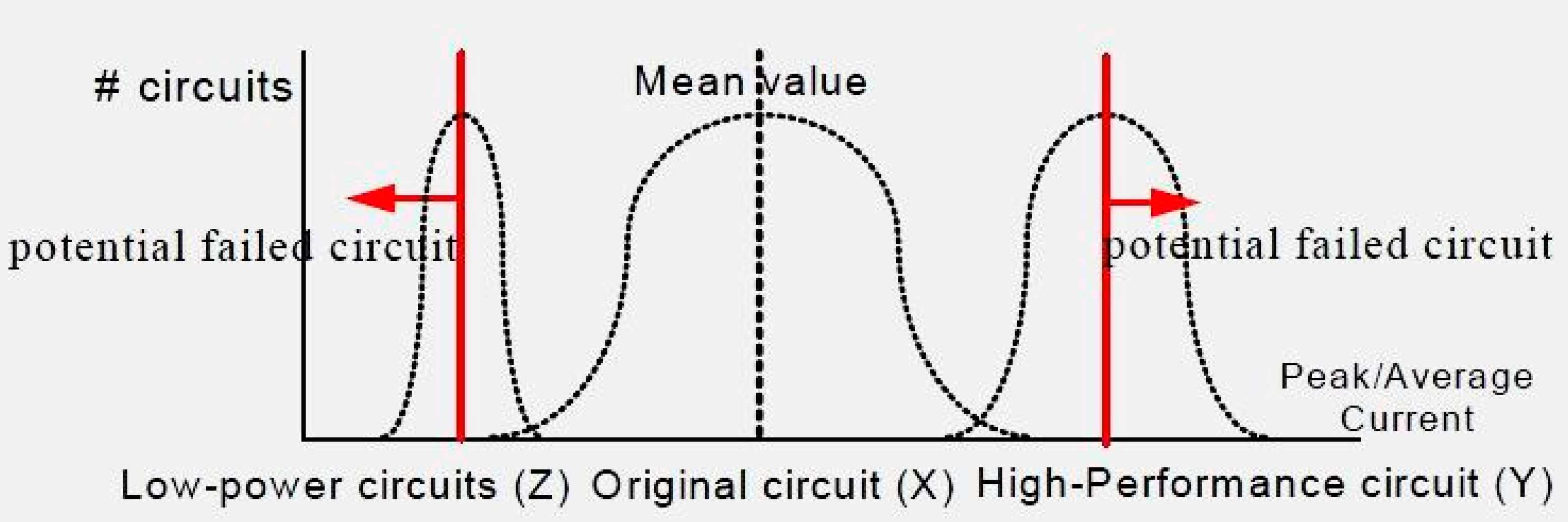
The current values may be in a uniform distribution waveform for most chips, and the waveforms differ for different chips. In order to clarify the current information for monitoring abnormal test chips, there needs to be a distribution waveform (outlier) with defined bounds. This is the current outlier for each design, and the ±3ó or ±6 deviation tolerance is considered during chip testing, as shown in
Figure 2. For such chips, the measured I
peak and I
avg are closed to the current outlier. A detailed retest is required to prevent the chip-testing quality problem.
The I
peak and I
avg screen concept is introduced in
Figure 2. The low-power design (LP-circuit) can be a lower bound of the original design (ORI-circuit). The high-performance design (HP-circuit) can be an upper bound of the original design (ORI-circuit). The current value of ORI-circuit is X, and its normal current value should not exceed the Y value of an HP-circuit, nor should it be less than the Z value of the LP-circuit reported value. The Y and Z values are the upper-bound and lower-bound references, respectively. The measured values I
peak (or I
avg) are between Y and Z.
Assuming that the current consumption is within the normal distribution range for the test chips, closed bounds need to be determined to screen the failed chips more accurately (to prevent over/under kill results). The proposed pretest stage technique can determine the current bounds for different types of designed circuits.
Our proposed technique provides reference bounds of the Iavg and Ipeak. As chips’ current consumption falls along a distribution, the referenced current-bound gap is not absolutely isolated. This means the current-bound regions might overlap. This type of situation leads potentially faulty results for the test chip, and therefore, it is necessary to carefully evaluate chips’ measurement results that are located in the boundary region of the distributed curve.
Before the chip testing phase, the Ipeak and Iavg information (values) may be obtained from the chip designer. However, when considering the fault coverage issue, the designer designated verification patterns might not be the same as the test patterns used during the chip testing stage. Hence, the Ipeak and Iavg need to be re-evaluated during the chip testing phase to identify abnormal peak and average currents of faulty chips.
The VT is the dominant source of circuit power consumption and circuit performance. The Ipeak and Iavg increases are linearly dependent on the quantity of normal VT gates. Multiple threshold voltage (MTCMOS) is a well-known, broadly-used design technique. Generic design technique proposes the gate VT-adjusting technique for low power consumption. The MTCMOS technique controls the thickness of the gate oxide (SiO2) of the CMOS transistor. This allows the transistor threshold voltage to be adjusted. There have not been any studies concerning the application of multiple threshold voltage CMOS (MTCMOS) circuit current consumption as bounds in order to evaluate other designed circuits under testing.
The drain-to-source current (I
DS) formula is shown in Equation (1). From the threshold voltage-adjusted technique, the lower V
T causes a higher I
DS for a shorter circuit delay time and higher power consumption designs. The higher V
T allows for the use of a lower I
DS current for lower power and longer circuit delay times. The high-threshold voltage can be used to design low-power and noise-immune circuits [
2]. Equation (1) shows that, by increasing the threshold voltage, the peak and average current values can be effectively reduced. Hence, the MTCMOS technique can be effectively used to reduce I
peak and I
avg:
The observations show that, when most of the logic gates use the normal-threshold voltage (VT) in the circuit, the current consumption increases and the circuit delay time decreases. When Tsize decreases, there are large current saving gains and the delay time increases. However, fewer gates using normal VT dominate the circuit performance (operation frequency). When most of the gates use high VT, the circuit current consumption is determined by these gates. Hence, the whole circuit current consumption is lower for most of the gates in an IE-circuit using high VT with small Tsize.
The circuit re-synthesis technique is adopted under a performance constraint in this proposed framework. The Ipeak and Iavg can be effectively reflected by adjusting the VT with gate transistor’s sizing (TSIZE) techniques. From the threshold voltage-adjusting and gate-resizing techniques, the Iavg, Ipeak, and area can all be reduced. The VT-adjusting and gate sizing techniques are under a positive delay slack time, and the circuit delay time does not increase.
The gate transistor’s resizing technique uses the greedy algorithm. By defining the logic gate slack time symbol as φ during the gate-resizing process, the gate with the largest φ is selected for replacement with a small driving gate in noncritical paths. The gate with the lowest φ is resized to a large driving gate in critical paths. This process maintains the circuit performance and decreases the transition current value. We show that the threshold voltage-adjusting and gate-resizing techniques can effectively estimate the Iavg and Ipeak.
The objective of the proposed software framework is to find an efficient methodology with in-house tools to analyze and degrade the Ipeak and Iavg concurrently. For example, if the synthesized circuit uses a low VT with a large transistor size, the Ipeak and Iavg currents increase. This framework has two purposes. For the test purpose, by applying dual threshold voltage and gate-resizing techniques, this proposed methodology can also be utilized to generate the peak and average current bounds while considering the circuit delay time and area. The second purpose is utilized to generate IE-circuit optimized design, which lowers the short, dynamic, and static leakage power consumptions without sacrificing system performance.
Each power rail can provide a limited current. When the gates consume a maximum current over the power rail design, then the power supply provides less current. This results in a voltage drop, and thus creates a gate delay. We propose that the circuit total Iavg and Ipeak need to be calculated from logic gates that transition at the same time interval, so accurate Iavg and Ipeak calculations should take the gate delay into consideration.
By using a quick incremental static timing analysis (STA), the slack time calculation speed increases. Nonlinear static or dynamic timing analysis techniques along with a dual VT cell library provide two kinds of accurate delay time calculation methods that are examined in this paper. The proposed technique has been divided into two parts: analysis and alleviation processes for Ipeak and Iavg.
Accurate Ipeak and Iavg information is needed for a transistor-level circuit simulation. However, this type of simulation requires a great deal of time and cannot be applied to large test circuits. The proposed frameworks can be used to solve the above problem for a large test chip. From gate-level estimation, this software framework has been proven to be highly accurate in comparison to a Nanosim (a transistor-level simulation tool).
The proposed methodology tries to toggle the logic gates as much as possible for emulating the real circuit operations. The input patterns are not as random as those of most conventional tools. Using this exhaustive technique to drive the tested circuit is unnecessary, as this is excessively time-consuming. In this proposed technique, the automatic test pattern generation (ATPG) is used to generate the essential and representative test patterns. This technique applies the generated evaluation patterns using the stuck-fault model from the ATPG and then applies the Ipeak and Iavg evaluated patterns into the circuit.
The reference current bound values need to cover the functional mode’s corner cases in order to be applied during testing phases. It also suggested that the test engineer needs to cooperate with the designer and apply the circuit’s functional test patterns during the testing phase. This method has the same design phase behavior as applying the circuit simulation pattern during the chip testing stage.
The static leakage current issue is not covered in this paper. However, the leakage current is an issue of genuine concern during chip testing. The leakage current measurement is found to be insufficiently accurate during the circuit simulation phase. The leakage current is postponed, while applying management requires a period of time when applying test patterns to the circuit during the practical chip testing stage. The duration depends on the characteristics of the circuit and applied process technology.
The focus of this framework is a rapid methodology for quickly estimating the Iavg and Ipeak current for normal chips. These proposed software tools effective screen potentially faulty chips and reduce the lengthy testing time for large circuits.
For deep submicron technology, manufacturing variation has a major impact on circuit performance and current consumption. When threshold voltage and transistor size are altered from the process variation, and the current distribution outlier is changed. The proposed reference circuit applies these variations to the simulation by altering the transistor high-/low-threshold voltage assignment and gate-resizing. Future work needs to integrate this consideration into simulations.
2. Literature Review
Figure 3 illustrates the function with respect to altering the transistors’ V
T and T
size for the 0.18-μm technology [
3].
An algorithm [
2] was proposed that determines the clock arrival time at each flip-flop in order to minimize the current peaks while respecting timing constraints, as shown in
Figure 4. Benchmark circuits show that current peaks can be reduced by more than a factor of two without penalty in terms of cycle time and average power dissipation.
An opposite-phase scheme for peak current reduction was proposed in [
4]. The basic idea is to divide the clock buffers at each level of the clock tree into two sets: Half the clock buffers operate at the same phase as the clock source, while the other half operate at the opposite phase of the clock source. Consequently, this technique can reduce the I
peak of the clock tree by nearly 50%, with the current waveforms shown in
Figure 5.
References [
2,
4] proposed an efficient I
peak reduction technique that uses the useful clock skew to shift the I
peak generation location. This technique does not take into account that the waveform dimension magnitude is similar. This leads to a reduction in the highest peak current, but not in power reduction.
Literature sources define CLUSTVAR (Cluster Inclined Supply and Threshold Voltage Scaling with Gate Resizing) [
5] as an algorithmic platform for power optimization by using dual supply voltages, gate sizing, and dual threshold voltages. CLUSTVAR can find a circuit status with the lowest dynamic and leakage power consumption on the premise that the circuit will not reduce performance or violate timing constraints. By demonstrating combinational circuits in the MCNC′85 benchmark suite, the savings of dynamic and leakage power are up to 42% and 67%, respectively.
The CLUSTVAR contributes to further power reduction. In CLUSTVAR, the algorithm is developed based on a maximal-weight independent set. However, the CLUSTVAR only considers the combinational circuit. The CLUSTVAR technique is STA-based. Conventional STA tools often provide pessimistic results and are only suitable for general-application designs. The traditional STA computations would require that all of the nodes in this circuit be recomputed due to the circuit delay time global impact, as shown in
Figure 6. This is due to the fact that simplifying the STA calculation reduces the gate-delay re-computation time.
In [
6], the methodology includes an explanation of how to set the quiescent current (IDDQ) bound to detect defective parts without rejecting defect-free parts. The proposed methodology increases design efforts for accurate standard cell library characterization with respect to power. The study does not consider that the accurate value is difficult to obtain, as the physical implementation issues (delay time, gate loading) cannot be accurately computed in the early design stage.
In [
7], tests for input threshold voltages are used to distinguish the characteristics of a device during validation, as well as the quality of a device during production testing. The paper focuses on the input threshold voltage issue, but does not take the internal core circuit into consideration.
Reference [
8] provides a survey of several outlier analysis techniques and compares their effectiveness in the context of delay testing.
A method is elucidated in [
9], in which the combinational circuit simultaneous switching operations are minimized. The delay slack times of the paths and clustered paths have similar slack values. The proposed register-transfer level (RTL) method takes advantage of the logic-path timing slack to reschedule circuit activities, thereby minimizing value within timing intervals.
Spreading the clock-tree drivers’ switching activity while maintaining a low clock skew at the clocked tree’s sink-nodes is proposed in [
10]. The clock-tree driver’s switching characterization has been used for fast computation of peak currents. A mix of high-threshold voltage and low-threshold voltage clock-drivers to minimize clock skew is employed in [
1].
In [
9], the objective is to reduce the number of glitches from the clock skew scheduling in a circuit, thus reducing dynamic power. The scheduling is formulated according to an integer linear programming problem, and the vector-independent clock skew schedule is derived to reduce glitches.
The studies [
9,
10,
11] are related to the proposed technique. However, their motivations are different. Contributions to the power reduction are made in [
9] and [
11], but not for the peaking current.
The above techniques most commonly used in the past only focus on Ipeak or Iavg reduction, i.e. one target in a circuit optimization stage. The generic low Iavg technique decreases the current waveform dimensions. However, the Ipeak reduction technique reduces the highest current value. Hence, the generic low Iavg technique cannot effectively reduce the Ipeak. The generic Ipeak reduction technique also cannot effectively reduce the Iavg.
For the Iavg and Ipeak estimation issues, the proposed technique is different from the above-mentioned studies and has several advantages. The proposed gate-level is approached after the circuit has finished the back-end synthesis stage and the gate-level information is extracted and calculated. This methodology will be more accurate if it is compared to the higher (RTL) design phase. Hence, the increased accuracy and computation time reduction targets are both achieved through the proposed framework.
3. The Proposed Current-Bound References Generation Technique
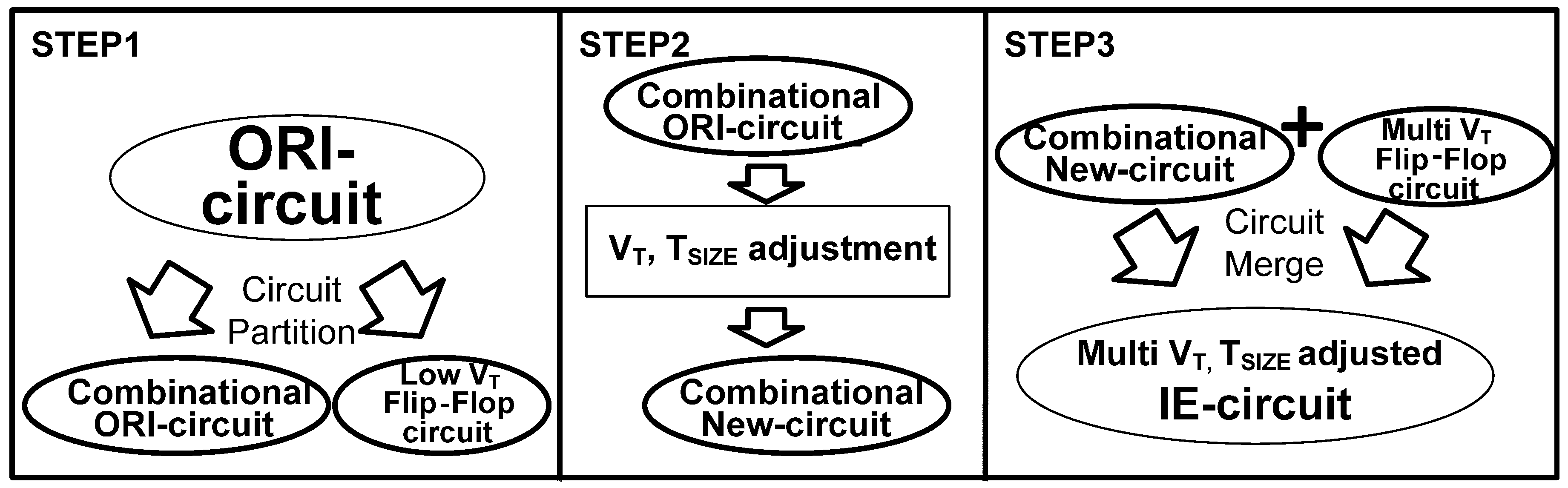
Circuit-testing engineers require an accurate and fast estimation tool to reprocess designed circuits into five reference circuits to find appropriate current bounds. In this paper, the proposed framework can quickly estimate the current bounds to support a fast screening technique to identify potentially faulty chips.
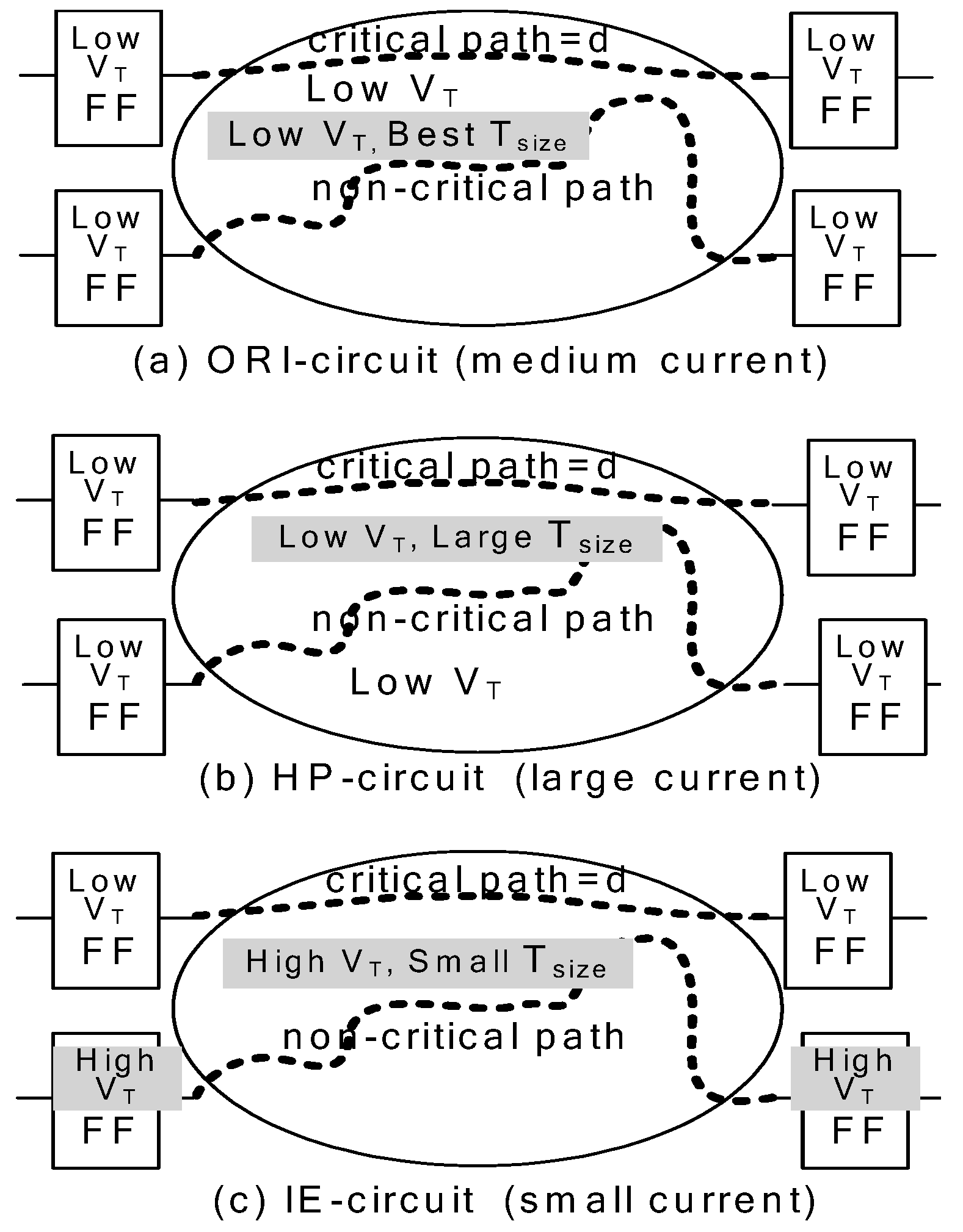
The proposed framework adopts threshold voltage-adjusting and gate-resizing techniques to re-synthesize five reference circuits, which are high-performance (HP-circuit). The large-TSIZE and low-VT transistors are used in this circuit. The ORI-circuit is an original-designed power-performance optimized circuit that uses best-TSIZE and low-VT transistors. The current reference design (IE-circuit) is a reference circuit for Ipeak and Iavg estimation, which is designed by using both TSIZE- and VT-adjusted transistors.
The re-synthesized IE-circuit can accurately estimate the Ipeak and Iavg and effectively perform Ipeak and Iavg reduction, using the threshold voltage (VT) adjustment with transistor sizing (Tsize) techniques under the same circuit’s performance constraint. The noise-immune design (NI-circuit) uses the best-TSIZE and high-VT transistors. The low-power design (LP-circuit) is a low-power designed circuit, which uses the small-TSIZE and high-VT transistors.
The low VT or high VT means the transistor is designed for low- or high-threshold voltage, respectively. The used TSIZE represents the circuit’s area; best-TSIZE means that the synthesized circuit uses the area-optimal constraint for a small area. Based on this synthesis methodology, if we design an LP-circuit, the IE-circuit’s reported value can serve as the reference upper bound, and the measured currents of the LP-circuit are not higher than the reported IE-circuit values. The Ipeak and Iavg closed lower bounds are the lowest Ipeak and Iavg values of the ORI-circuit working at the same clock frequency.
They are re-synthesized from the ORI-circuit. Once the original design (ORI-circuit) is ready, the test engineer utilizes the proposed framework to re-synthesize the ORI-circuit to the IE-circuit HP-circuit, NI-circuit, and LP-circuit. The IE-circuit is an adjusted VT and TSIZE circuit by adopting the MTCMOS approach from the ORI-circuit, IE-circuit current consumption serves as a reference for the other four designed circuits. After determining the Iavg and Ipeak current values of the IE-circuit from simulations, the obtained current values can then be used as a comparison value of the designed chips during the testing stage.
The IE-circuit is a power-performance optimized reference circuit. In IE-circuits, the gates that do not dominate performance are replaced with gates that have high-VT and small-TSIZE for lower Ipeak and Iavg. This technique uses the longest circuit delay time as the constraint. As the IE-circuit has low Ipeak and Iavg, without performance degradation, it can be applied as a closed lower bound for the ORI-circuit. The proposed IE-circuit with the VT and TSIZE adjustment technique does not increase the circuit delay time, and Ipeak and Iavg decreases concurrently.
In this paper, the proposed IE-circuit can be used during chip testing to classify faulty chips. The IE-circuit has the same performance as the original designed circuit under testing. Only the threshold voltage and transistor size are altered from NI, LP, or HP reference circuits.
4. The Current-Bound Reference Circuits Generation Method
The characteristics of the proposed framework are twofold. The first is a quick and accurate Iavg/Ipeak estimation technique. The second is the designed circuit Ipeak and Iavg alleviation technique to reduce the Iavg/Ipeak current values. The proposed dynamic timing incremental analysis methodology can quickly and accurately identify the Ipeak and Iavg of an application circuit.
There are five types of circuits adopted in this paper. The
ORI-circuit is the original circuit synthesized by using generic cells based on design flow. All gates use low-V
T and simplified logic circuits with optimal driving capabilities. The
HP-circuit is designed for high performance. It is synthesized by using low-V
T for all logic gates while enlarging the gate size for higher driving strength. The
LP-circuit with all high-V
T and minimized T
SIZE cells has the least power consumption and a low peak current. The
NI-circuit uses the best-T
SIZE and high-V
T transistors for higher signal noise tolerate ability. These circuits are shown in
Figure 7.
LP-circuit is designed with high-VT and uses a small driving ability gate (small-TSIZE) for the lowest Ipeak and Iavg consumption. NI-circuits use High-VT with the same TSIZE as ORI-circuits. The NI-circuit uses High-VT gates that have best-TSIZE. The Ipeak and Iavg decrease, and circuit delay time increases. The LP-circuit, in contrast to the NI-circuit, minimizes the TSIZE for lower Ipeak and Iavg, but also increases the delay time. The difference between the NI-circuit and the LP-circuit is TSIZE.
For the proposed technique, the first target is Iavg and Ipeak current estimations, and lowering the average power has also been taken into consideration. The proposed software framework target is to generate (re-synthesize) several reference NI-, LP- and HP-circuits as the measurement reference bounds to the original designed circuit (ORI-circuit) during the test-circuit testing stage.
The gate-resizing method is adopted to choose different driving capability cells in the library. The threshold voltage reassignment and gate-resizing techniques are executed from the ORI-circuit, and are then re-synthesized by applying the proposed framework.
We focus on the IE-circuit generation method in this paper. The IE-circuit is a multi-VT designed circuit that uses adjustable VT and gate sizes. The IE-circuit has optimal performance with Ipeak and Iavg consumption. The proposed framework is used to synthesize all of the above circuits for comparison purposes.
The VT- and TSIZE-adjusted technique impacts the Ipeak, Iavg, and power consumption. The IE-circuit uses the VT-adjusting and TSIZE sizing techniques. IE-circuits have larger-TSIZE than NI-circuits and LP-circuits under a certain delay requirement. Thus, the Ipeak and Iavg are larger.
As
Table 2 shows, the peak current and power consumption of IE-circuits are in the middle range of the five circuit types. The IE-circuit does not change the critical circuit path delay times. The IE-circuit is a good reference circuit under the same ORI-circuit performance constraint, but with the lower I
peak and I
avg current consumption.
After determining the average measured current from the sample’s physical ORI-designed test chip, simulation bound values can then be used to set the bounds for chip testing equipment. The software framework reported values are used as references to set the upper and lower current bounds during the chip testing phase.
The Reference IE-Circuit Generation
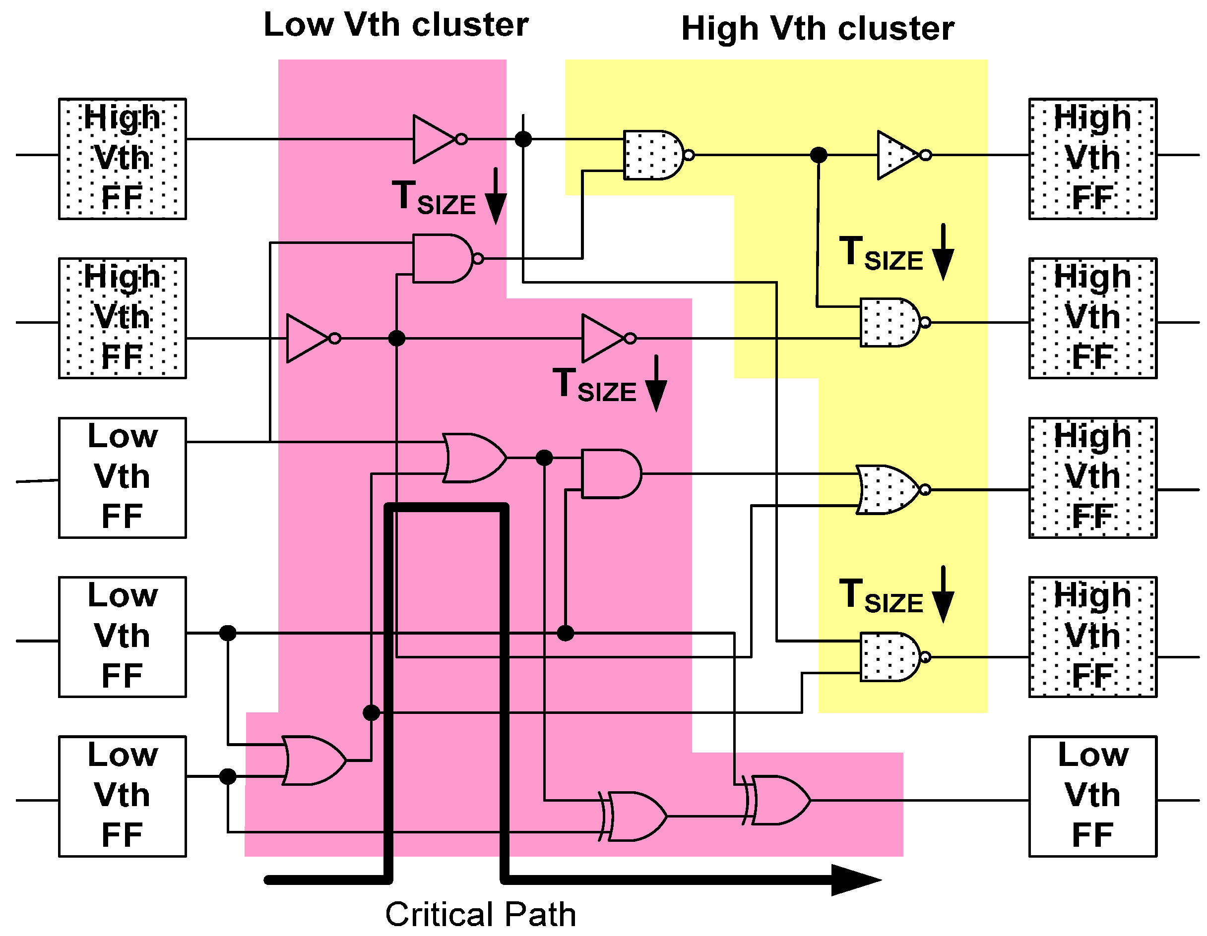
Most of the Ipeak and Iavg comes from the flip-flop (FF) state transition. In this proposed technique, both the FF and logic gate VT are simultaneously adjusted to reduce the Ipeak and Iavg.
This proposed efficient framework of peak-current alleviation with a power delay and area reduction uses adjusted transistor threshold voltage and gate-resizing. The largest I
peak is generated from the flip-flops with prior stages of the logic gates’ input transitions at the same time. A high V
T gate has a higher circuit delay time with a lower I
peak than a normal V
T gate. The IE-circuit allows the logic gates in a noncritical path with positive slack time to replace the high V
T gate, as shown in
Figure 8.
The IE-circuit uses both the gate-resizing and threshold voltage (VT)-adjusting techniques to simultaneously attain Ipeak and Iavg reduction, power savings, and a smaller area. Iavg and Ipeak can be effectively reduced by changing MTCMOS gates or by changing MTCMOS gates, which have the same function but different driving capabilities (Tsize). The nonlinear dynamic timing analyses with incremental delay time calculation techniques can quickly and accurately estimate Ipeak and Iavg.
5. The IE-Circuit Delay Time Calculation
We propose the circuit total Iavg and Ipeak need to be calculated from logic gates that transition at the same time interval, so accurate Iavg and Ipeak calculations should take the gate delay into consideration. This technique has considered the different gate delays when there are varying VT.
Most traditional circuit delay time evaluation techniques are computed using STA. The traditional STA is pattern-independent from the worst-case estimation technique. However, this STA technique provides an excessively pessimistic evaluation of the circuit delay times. It is not suitable for designs used in specific applications.
The conventional STA counts the path delay by summation of all individual gate delays. This conventional STA calculates the circuit delay by summation of all of the gates’ delays based on a single threshold voltage source. This is referred to as the linear STA, which does not consider the gate delay difference from the threshold voltage variance of each gate.
The traditional STA computations would require that all the nodes in this circuit be recomputed because of the circuit delay time global impact. Hence, most conventional STA tools provide overly pessimistic results and are only suitable for general-application designs.
The circuit’s consuming current is related to the timing of the gate’s transitions. Accurate timing analysis can efficiently estimate the consuming current. The proposed technique simplifies the STA calculation and reduces the gate-delay re-computation time. Compared with the other gate-level tools, the proposed incremental nonlinear STA was used for quick and accurate estimates.
In a traditional design strategy, the circuit performance analysis relies on the longest path delay calculation by using STA/DTA. The voltage drop may not induce circuit delays, as not all gates in the circuit are affected by voltage drops. The path delay will not increase if the consumed currents of all gates do not exceed the power supply. Moreover, the circuit total delay will not increase if the increasing gate delay (due to lower voltage) is not located on the critical path. Thus, repeat timing recalculation by STA/DTA is not necessary for all paths. The proposed incremental STA/DTA technique focuses on the paths of concern to avoid the re-computation of many path delay times.
Two timing calculations are proposed in this framework. The first nonlinear STA (NLSTA) uses the table-lookup method to estimate the gate delay time, which is pattern-dependent. As the NLSTA technique is based on real circuit transition times, the estimation results are more accurate than STA by specific dependent applications. The NLSTA technique is needed to design a reliable chip without specific applications, such as for a CPU.
The dynamic time analysis (DTA) estimation results are close to the real application results. The second proposed nonlinear dynamic time analysis (NLDTA) technique is used for the pattern-dependent delay time calculation. NLDTA achieves the highest accurate estimations in comparison with the STA, NLSTA, and DTA techniques. However, the calculation time is the longest. The accurate voltage induced delay is a dynamic behavior that is pattern-dependent. NLDTA is a real application transition current. It is suitable for specific application designs. The NLDTA verification input patterns provided by a circuit designer may have lower logic state transitions than those of NLSTA.
From comparisons with the conventional STA technique, the proposed NLSTA and NLDTA have good computation time saving results. The nonlinear STA and DTA need more time to compute the circuit delay. However, the incremental technique can save a great deal of re-computation time.
For a generic designed circuit, the Ipeak and Iavg are pattern- or timing-dependent. The proposed NLSTA and NLDTA are pattern-dependent estimation techniques. This can solve the problem of the pessimistic estimation of the traditional STA.
5.1. The Proposed NLSTA and NLDTA Delay Time Calculation Techniques
The proposed IE-circuit technique applies threshold voltage-adjusting and gate-resizing to reduce Iavg and Ipeak. The gate delay, Iavg and Ipeak need to be re-computed for accurate estimation when threshold voltage varies. Moreover, the proposed technique uses the estimation of the current bound setting and then induces a supply voltage drop and a circuit delay time increase. Hence, an accurate and quick delay calculation technique is an integral element of our approach.
Good Ipeak and Iavg estimation input patterns (testbench) can activate a large number of gate switches (transitions) at the same time. These patterns trigger the circuit to generate the largest voltage drop. Our proposed methodology can quickly estimate the worst-case Ipeak/Iavg of the circuit using NLSTA/NLDTA.
The first step in the process is to define the circuit level from the topological sort and then sort the level according to Ipeak and Iavg. This is followed by computation and sorting by cost (COST) for all gates at each level. The gate-resizing and VT-adjusting processes are applied using the cost function of each gate. The cost function of each gate is defined by the equation COSTg = (Ipeak-before − Ipeak-after)/(Slackbefore − Slackafter). The computation formula is the same for the average current process. This cost function is also applied by changing Ipeak to Iavg when calculating average current.
The large cost function means that the gate contributes more to Ipeak (Iavg) reduction, and needs to be processed first. Ipeak-before (Iavg-before) and Ipeak-after (Iavg-after) denote the Ipeak (Iavg) of this gate before and after sizing, respectively. Slackbefore and Slackafter denote the slack time of this gate before and after sizing, respectively.
The procedure for the I
peak (I
avg) reduction process is as follows:
Repeat the process for the highest remaining value among the remaining levels until all levels are processed.
5.2. The Incremental Calculation Technique for the Proposed NLSTA and NLDTA
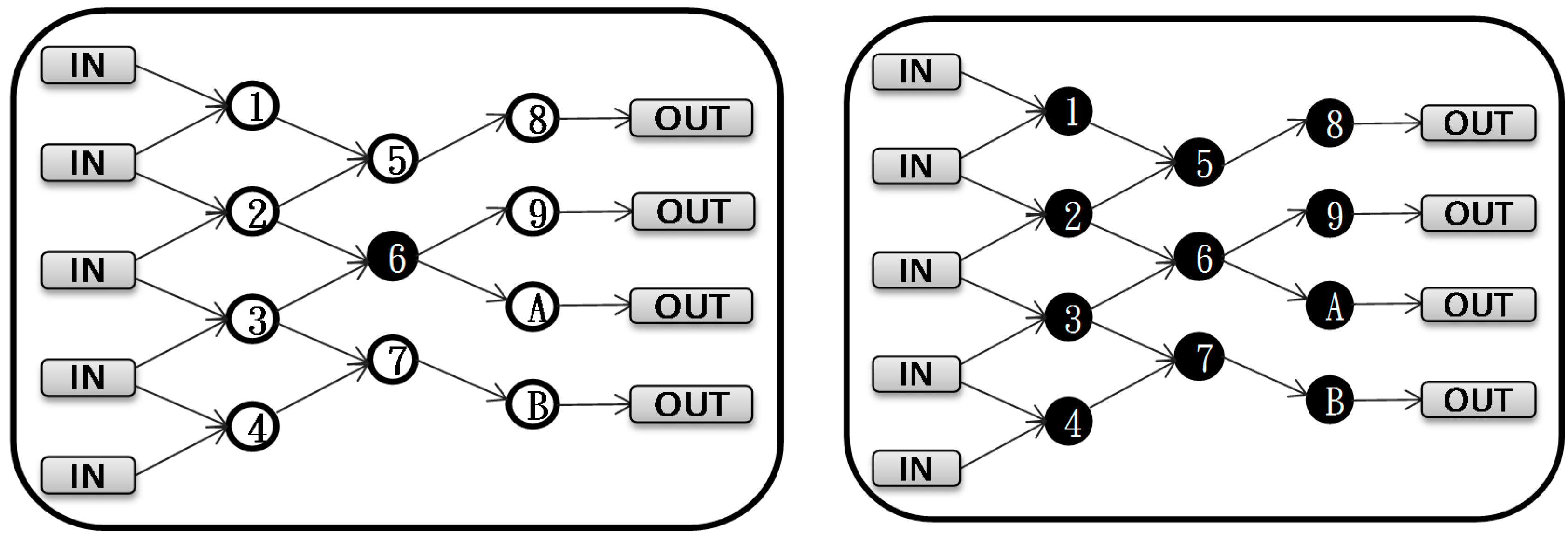
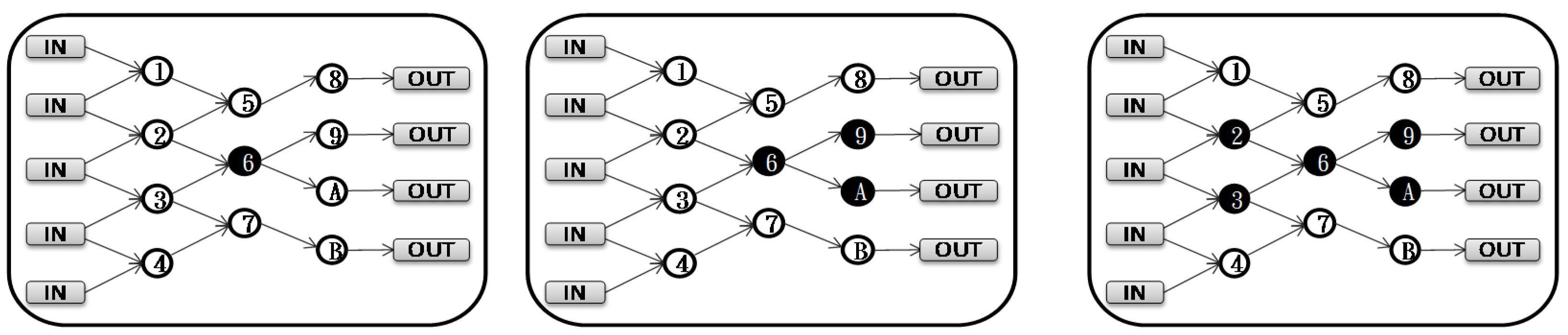
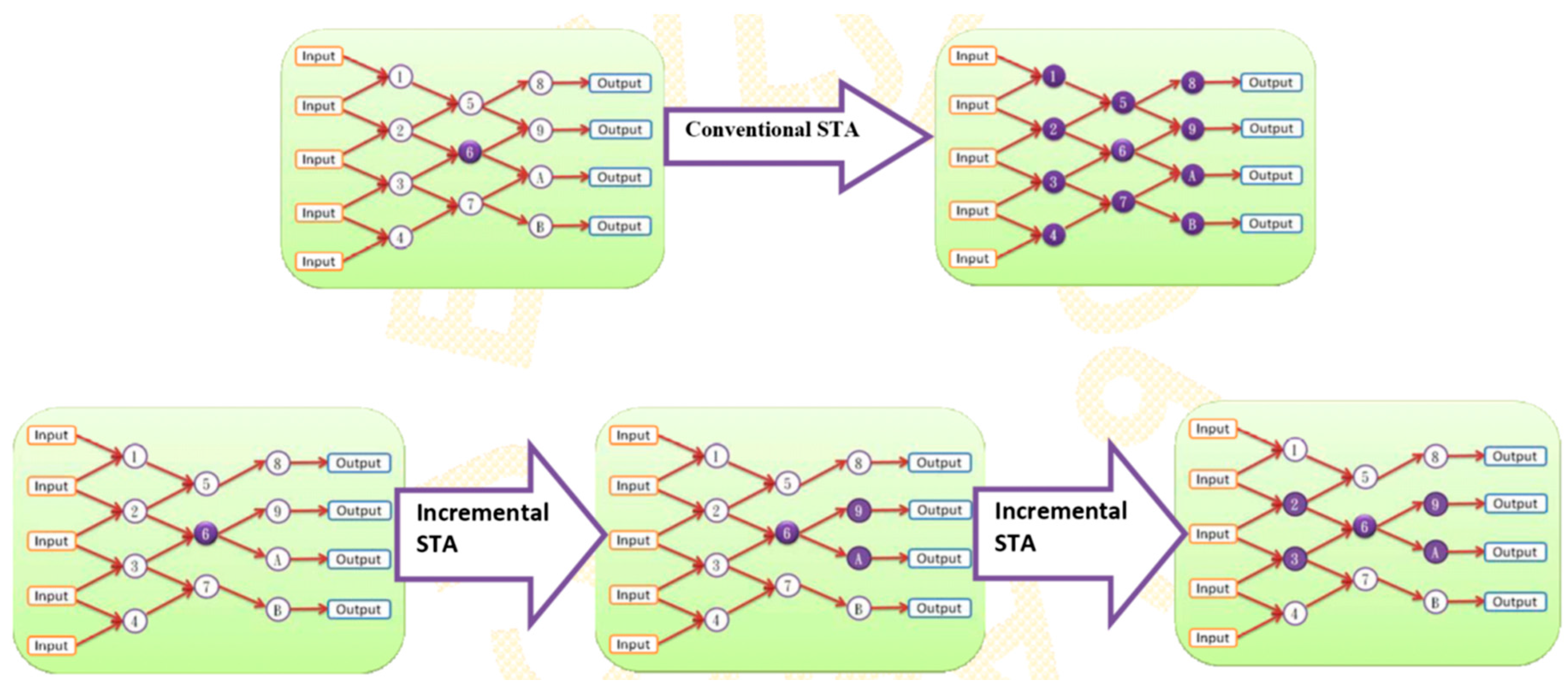
In conventional STA delay, timing re-computation is required if the node-6 gate information is changed. Due to the circuit delay time global impaction, the traditional STA computation modifies all nodes in this circuit that need to be recomputed. For the following incremental STA, the impaction is only on the fan-in and fan-out cones of this node, as shown in
Figure 9.
It is complex to dynamically recalculate the circuit’s delay by considering all gates using varied threshold voltage. This is due to the fact that VT adjustment will result in different gate delays. Then, the former estimated Ipeak and Iavg should be re-calculated due to the different gate delays (from varying VT). The re-computing process should be repeated until all of the gates are processed.
Dynamic timing analysis is required in order to consider the floating gate delay value under varying VT and Tsize. Dynamically re-calculating the circuit performance is time-consuming because of the high computation effort involved. This calculation time can be reduced by using the incremental NLSTA and NLDTA.
The proposed framework uses the non-linear STA to compute the accurate slack time, and the delay time can be found in the tables. From the execution time comparisons, there is less computation time for the large circuit.
The circuit tree data structure is mapped according to the timing-based gate topology. This tree can then be used for easy path tracing. The affected longer delay path can be easily found from the lowest leaf of the tree.
The proposed increment nonlinear DTA technique uses the table lookup technique to compute an accurate delay time. The proposed incremental technique only impacts the fan-in and fan-out cones of this node. Moreover, the dynamic nonlinear STA saves significant computation effort. The computation time comparisons are shown in
Figure 10.
6. The Proposed Software Framework of the IE-Circuit
IE-circuit is the only detailed discussed reference in this section. The functions of IE framework include the I
peak and I
avg alleviation process, which came from the close relationship between the I
peak, I
avg, and the gate delay. The V
T- and T
SIZE-adjusted techniques are used to reduce the current consumption with a lower I
peak, I
avg, and area, as demonstrated in
Section 5. After locating those logic gate levels with the largest I
peak and I
avg within the circuit gate forest, fast path delay calculation is carried out by combining NLSTA/NLDTA and the path sensitization algorithm. The largest I
peak and I
avg contributed gates are located by using Heap-Sort. When any gate V
T is varied or resized, the new path delay times are recomputed by applying an incremental timing analysis technique to the circuit hierarchy.
The Ipeak and Iavg alleviation and analysis tool includes two major functions. This software framework is written with C, sis, and Perl. The tools also combine the common interface with commercial tools, such as Synopsys and Nanosim.
The analysis feature includes the following functions:
gate-level function simulation;
consumption current report;
circuit delay timing report;
power consumption report; and
voltage/current waveforms.
The optimization feature includes the following techniques:
In this framework, the synthesis/analysis process of the cell delay uses the threshold voltage from the cell library, which is characterized from the TSMC 0.18-μm standard cell library. It is modified by calibrating the calculation formula and HSPICE simulation results. The intrinsic delay time is characterized by the gate simulation with no output load. The normal- and high-threshold voltages are 0.23 V and 0.44 V, respectively.
In
Figure 11, for a sequential circuit, the expanded combinational circuit part from the timing window and repeat the calculation process. Because the IE-circuit considers the delay time optimization of flip-flops, the circuit delay times do not increase after the flip-flop (high-V
T) replacement process.
For example, the LP-circuit is obtained from replacing the high-VT and small-Tsize logic gates for a lower Ipeak and Iavg. An optimization process is performed to minimize the Ipeak and the Iavg by substituting logic gates that have low VT and large Tsize instead of having logic gates that have a high VT and a small Tsize. High-VT and small-Tsize logic gates dissipate less Ipeak and Iavg, but also operate more slowly than low-VT and large-Tsize logic gates. Hence, multi-VT and Tsize optimizations are a trade-off between Ipeak, Iavg, and path timing.
As the Ipeak, Iavg computations have recursive relationships, they conform to the circuit’s path delay time. The optimization process is finished when the Ipeak and Iavg values are in a stable state. There is an approach utilized: When all circuit levels are evaluated and the range of delay times lies below a threshold (5%), the optimization recursive process is then halted.
The proposed software tool is not used to report the accurate values for the designed circuits. It is difficult to accurately compute the Ipeak and Iavg from a higher-level model. The software framework proposes the gate-level estimation and reduction methodology. This technique can also reduce the Ipeak and Iavg without the circuit delay time or area increase penalty. The proposed framework includes quick gate-level estimation functionality with transistor-level accuracy.
7. Experimental Results Analysis
The current-induced voltage drop not only induces circuit delay and power, but also reduces the circuit noise margin from a lower supply voltage and raises the issue of reliability from electro-migration. The framework proposes a fast gate-level estimation and reduction technique, which merges the Iavg, Ipeak, and nonlinear static/dynamic timing analysis. From the proposed framework, fast and accurate estimation results are determined for five types of re-synthesized circuits. There are ten test circuits used to demonstrate the efficiency of IE methodology. Among nine of the ISCAS89 benchmark circuits, the VLD circuit is the variable-length video decoder design.
The sizes of the tested circuits are listed in
Table 3. The experimental circuits are optimally synthesized by circuit synthesis tools (sis and
Synopsys). The sizes are different for all circuit logic gates.
The commercial circuit simulation tools are included as a reference for comparison and to allow us to evaluate our tool’s accuracy. The computation time information is shown in
Table 4; the computation time is very short when using our proposed tool.
Table 5 and
Table 6 show the gate-level circuit estimation results of peak and average current consumption for the five types of circuits. Based on the TSMC 0.18-μm process, the clock frequency is 20 MHz for all circuits. Two thousand ATPG test patterns are used for the test circuit.
Column 3 in
Table 5 and
Table 6 shows the peak current and power consumption of the ORI-circuit, respectively. Columns 2, 4, 5, and 6 show the ratios of comparisons for the four types of circuits with an ORI-circuit. These results are used as the basis for the following comparisons with the ORI-circuit. The following values mean that the specific circuit reference values are multiplied by the values of the ORI-circuit. As shown in the example in
Table 5, the reference I
peak for HP-S27, IE-S27, NI-S27, and LP-S27 are 2.78 mA (2.21 × 1.26 mA), 0.81 mA (0.64 × 1.26 mA), 0.72 mA (0.57 × 1.26 mA), and 0.39 mA (0.31 × 1.26 mA), respectively. The major contribution of this tool is to provide the tightened lower reference bound for the current outliers in the designed circuit.
Table 5 and
Table 6 indicate that the HP-circuit is a high-performance one. Its I
peak and I
avg current consumptions are larger than those of the other proposed circuits. These values can be referred to as the upper bounds of different circuits. IE-circuit optimization technique reduces the circuit I
peak and I
avg current consumption. The IE-circuit is closer in value to an ORI-circuit. For low-power (LP) and noise immune (NI) MTCMOS circuits, the IE-circuit can serve as the upper reference values of the I
peak and I
avg currents.
Table 5 and
Table 6 also indicate that the IE-circuit is the median value of the five types of circuits. IE-circuits can be good a reference during a circuit test phase and can quickly filter out the failed chips. The IE-circuit uses dual threshold voltage with gate-resizing for I
avg, I
peak, power, delay time, and area reductions without increasing overhead delay time.
The
Nanosim circuit simulation results are taken as the golden values. Although the IE-circuit uses the gate-level estimation method, we show high accuracy in comparison to
Nanosim, as presented in
Table 7. The software framework provides good estimations. The I
peak and I
avg consumption estimations are 1.87% and 9.66% lower than
Nanosim estimations, respectively. An efficient I
peak and I
avg reduction methodology and accurate in-house EDA analysis tools are proposed in this paper.
As shown in
Table 8, the computation time of the IE-circuit is 334 times faster on average than that of
Nanosim. The quick and accurate estimation results help designers to quickly predict a circuit voltage drop.
In this work, several benchmark circuits’ evaluation results have been provided. Practical chip measurement results are not shown in this manuscript. It is recommended that physical chip validations be examined in detail in a separate future study.
8. Discussion of Test Application Using the Proposed Techniques
A complicated preparation process is required to test the chip and to evaluate whether the chip is functionally workable. Furthermore, the proposed technique assists the test engineer to quickly screen out the failed chips from using the chip’s consuming current values and to determine the lower and higher current values for normal chips during the chip measurements. The proposed method can also be used for the chip binning situations.
In this research, both the Ipeak and Iavg values can serve as effective references for judging a failed chip during testing. Thus, current consumption observations can be helpful for quick screening of potentially failed chips in the testing phase. The current estimation technique generates current bounds suitable for reference from transistor threshold voltage and size adjustment. The feasibility of the proposed bounds will require further detailed examination, which could be addressed in a future work.
An abnormally large Iavg and Ipeak current induces a voltage-drop and impacts the circuit delay time and reliability. This paper presents Iavg and Ipeak estimation and reduction techniques based on TSIZE and VT selection. As a chip’s current consumption is a distribution, the proposed technique provides reference bounds for the Iavg and Ipeak, and these referenced current-bound gaps are not absolutely isolated within the HP-, NI-, and LP-circuits. This means that the current-bound region might overlap. This type of situation leads to potentially faulty results for the test chip; therefore, it is necessary to carefully evaluate chips’ measurement results that are located in the boundary region.
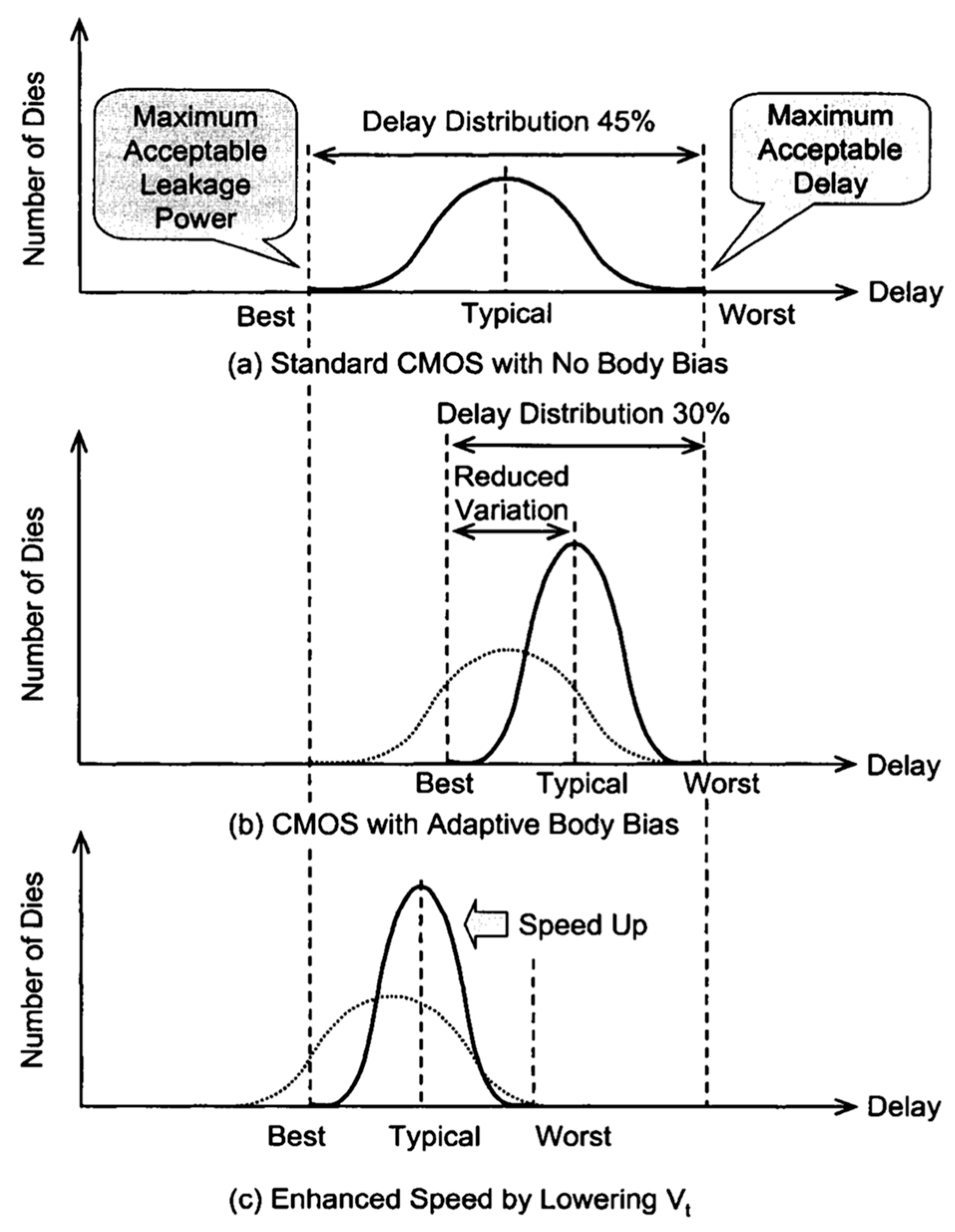
When the transistor’s body-bias is altered, there is the V
T disparity in the process variation, the wafer’s die-to-die delay time variations are shown in
Figure 12. Our study does not take the process variation into simulations. This also leads to the inaccuracy estimation, and a feasible methodology is needed to add ±3σ statistic variation parameters into the emulations.
The leakage should be accommodated for advanced process in a future study. The manufacturing variations in the circuit’s simulation have not been included here. These factors need to be included in a future study.
There are several claims addressed in this paper:
- (1)
The proposed technique identifies the transition gate and includes the gate’s timing and average- and peak-current in the calculation. When calculating the Iavg and Ipeak, the proposed method partitions a circuit level by level, and then sums the Ipeak at every level. However, due to the different delays of various gate types, gates of the same level do not necessarily switch at the same time.
- (2)
There are two steps during the testing chip operation with the proposed technique. In the first step, ATE quickly screens the tested chips by using current bounds. For chips that fail during the first step, the second step is conducted manually. We can view and retest the chips by monitoring the circuit function and current in detail to accurately recover any potentially good chips.
- (3)
In general, using TSIZE and VT change as a means of current reduction is more easily evaluated than other competing design constraints in low-power objectives, and it is suitable for advanced design technology. The input signal with a lower transition time (fast signal transition) has a lower Ipeak.
- (4)
The generic static timing analysis tool does not consider gate dual-delay for dual-VT cells for the path delay time calculation.
9. Conclusions
As the testing of chips requires a longer period of time, the proposed technique can assist an engineer in quickly screening for as many failed chips as possible. Using current bounds to screen for faulty chips is a comparatively novel idea, and the proposed schemes use it as a component in statistical outlier analysis. Observations of the Ipeak and Iavg currents are important for testing a circuit. However, previous research has focused on the discussion of the testing impact on power consumption, without upper or lower current bounds to screen for faulty chips. This paper proposes using the peak and average current bounds as the mechanism for a fast screening of potentially failed chips during the testing stage. The five proposed reference circuits provide Ipeak and Iavg references for an original designed circuit under testing. The IE-circuit shows that, from applications of the VT and TSIZE-adjusting techniques, the closed current bounds can be determined. There are less than 2% and 10% estimation errors, respectively, in the Ipeak and power (Iavg), with respect to the Nanosim (transistor-level) simulation results. The computation time of the proposed framework is 334 times faster on average than Nanosim. The software framework is a rapid methodology to estimate Ipeak and Iavg to solve the lengthy testing time problems for large circuits. The effectiveness of the proposed method for screening faulty chips needs to be justified in future studies.


