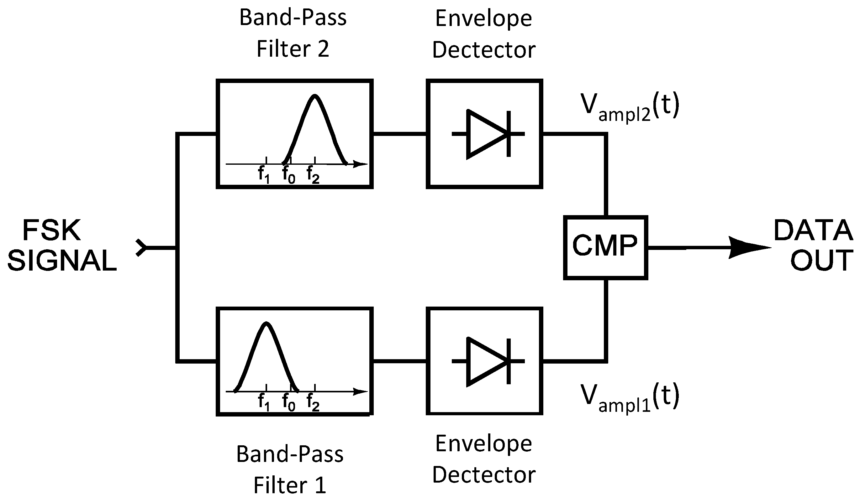
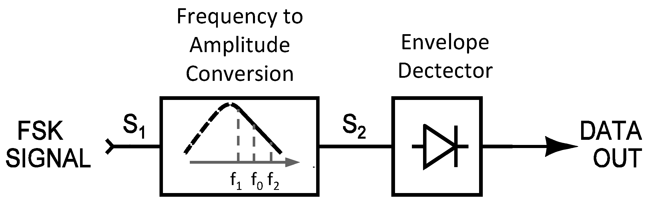
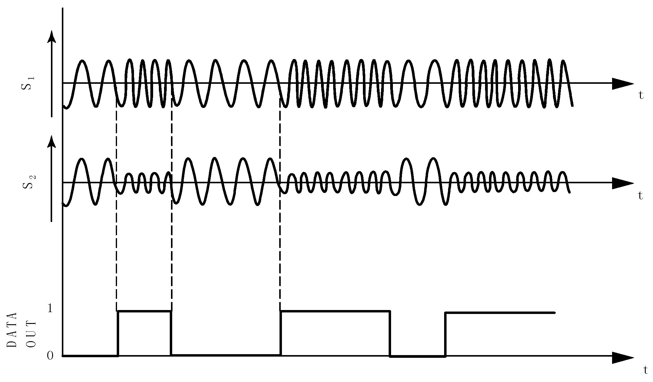
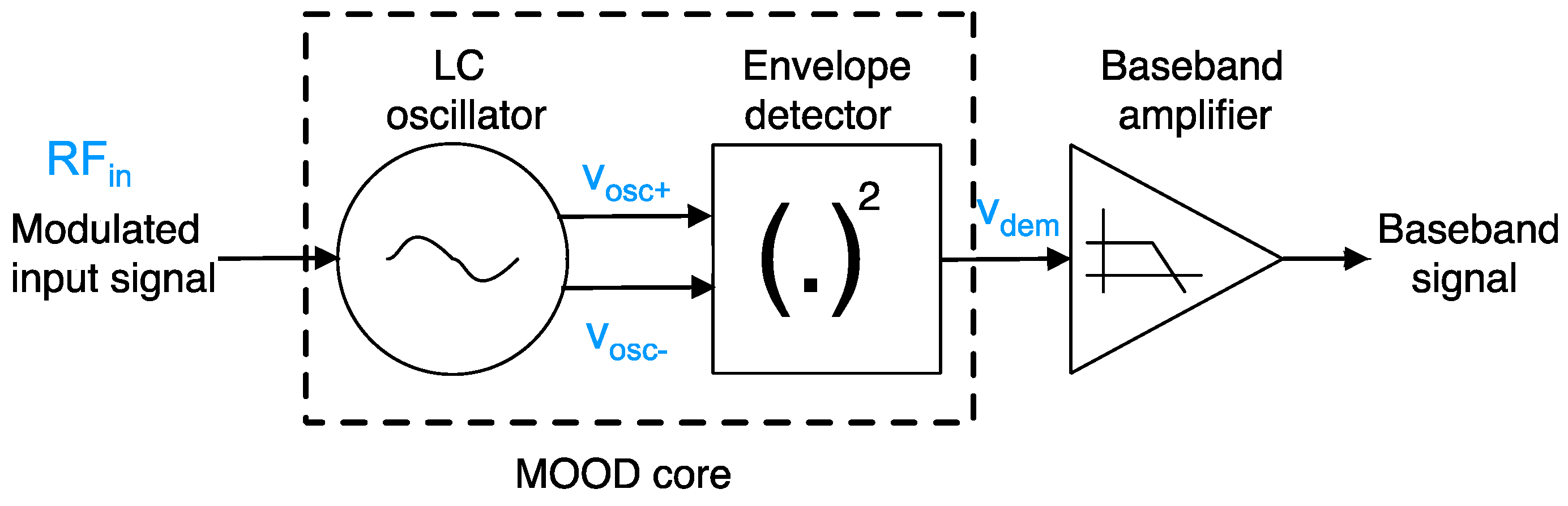
The demodulator architecture presented in
Figure 7, namely Modulated Oscillator for Envelope Detection (MOOD), exploits the principle of demodulation proposed in
Figure 4. It may be viewed as a Tuned RF receiver, where an LC oscillator is introduced before the envelope detector to perform an FM-to-AM conversion. It has been demonstrated this demodulation circuit is theoretically compatible with frequency and amplitude modulation schemes. As a proof of concept, this MOOD system is implemented in a 65 nm CMOS technology from ST Microelectronics, and is intended for 2.4 GHz ISM Band. This section further details the design strategy and the characterization of the main blocks featuring a MOOD receiver: the LC oscillator and the envelope detector.
Figure 7.
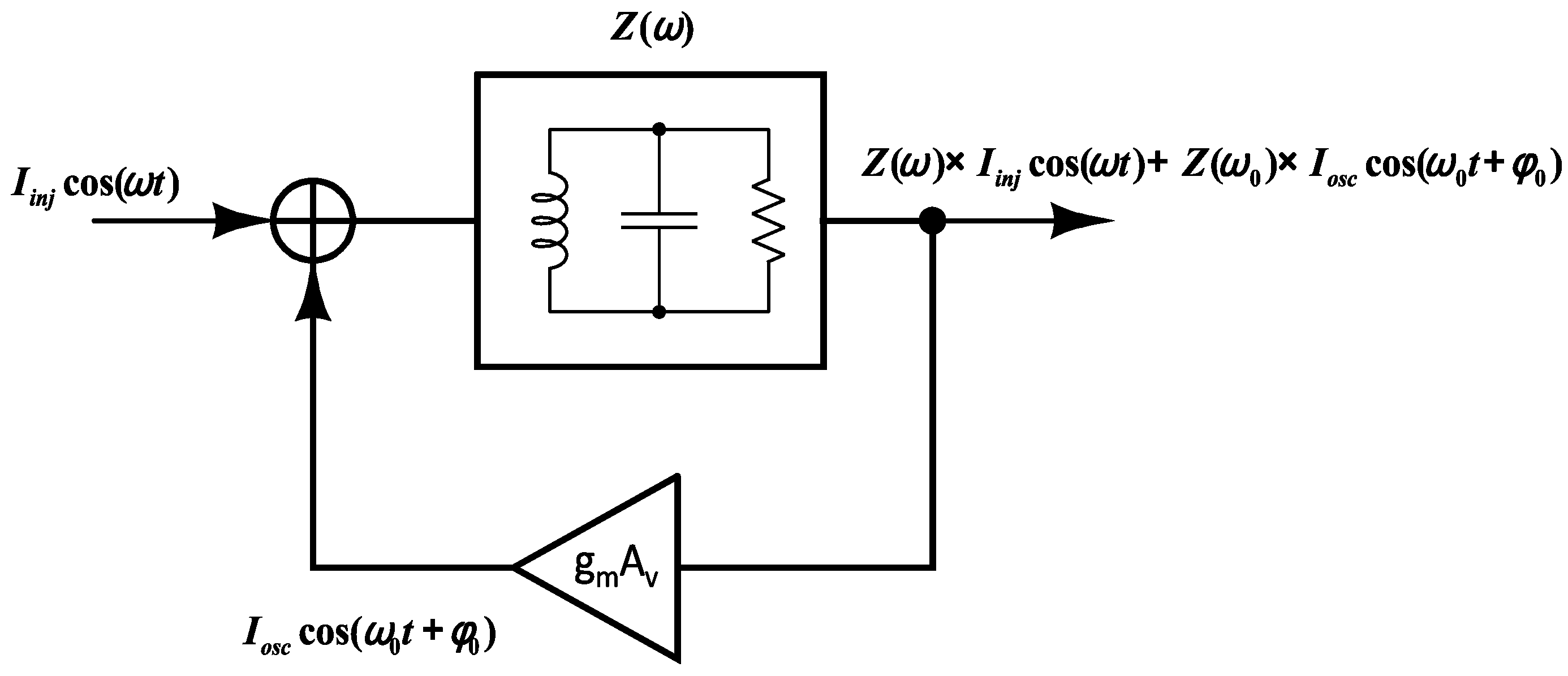
Simplified behavioral model for injection pulled oscillator.
3.1. Low Power LC Oscillator
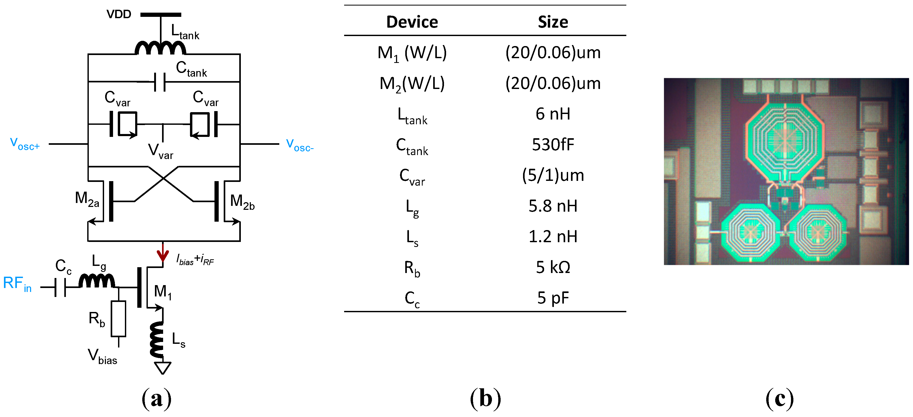
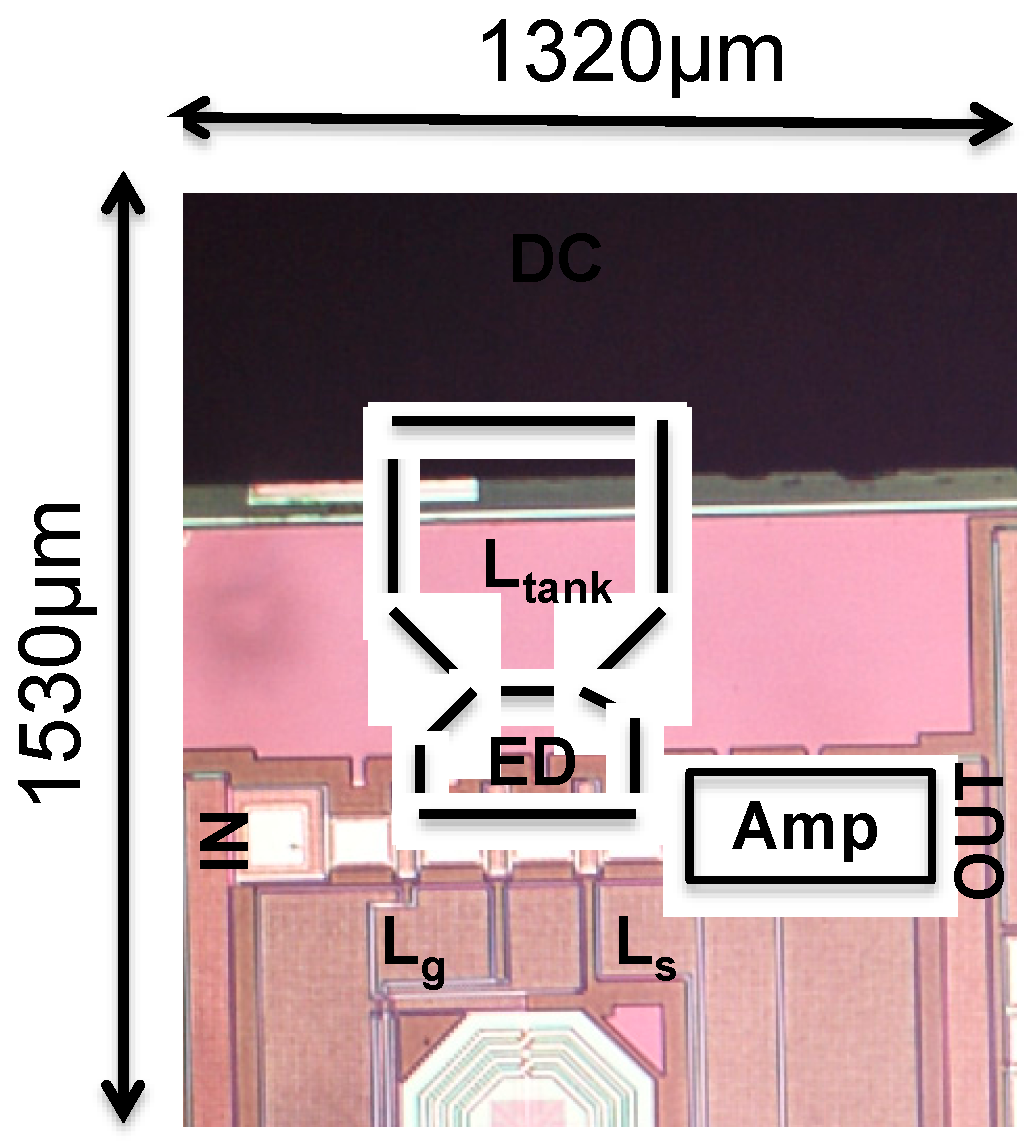
LC oscillators are very popular in wireless transceivers as they achieve a low phase noise due to the high energy-storage capability of LC tanks. A standard cross-coupled architecture is selected here for its immunity to supply common-mode disturbances. The schematic of the oscillator is presented in
Figure 8a and the device sizes are reported in
Figure 8b. The tank, formed by L
tank and C
tank, sets the free running oscillation of the oscillator, which is fine tuned by C
var. The cross-coupled pair (M
2a, M
2b) compensates for the loss of the tank and sustains the oscillation. The transistors M
2i are sized to operate in moderate inversion region to achieve a best trade-off between performances and current consumption according [
12]. The transistor M
1 steers the tail current and injects the external signal RF
in applied to its gate. The inductors L
g and L
s perform the 50 Ω input matching. A micrograph of the oscillator, implemented for a stand-alone characterization, is presented in
Figure 8c.
Figure 8.
Schematic of an LC cross-coupled oscillator with RF injection (a); device size (b); micrograph of the oscillator (c).
Figure 8.
Schematic of an LC cross-coupled oscillator with RF injection (a); device size (b); micrograph of the oscillator (c).
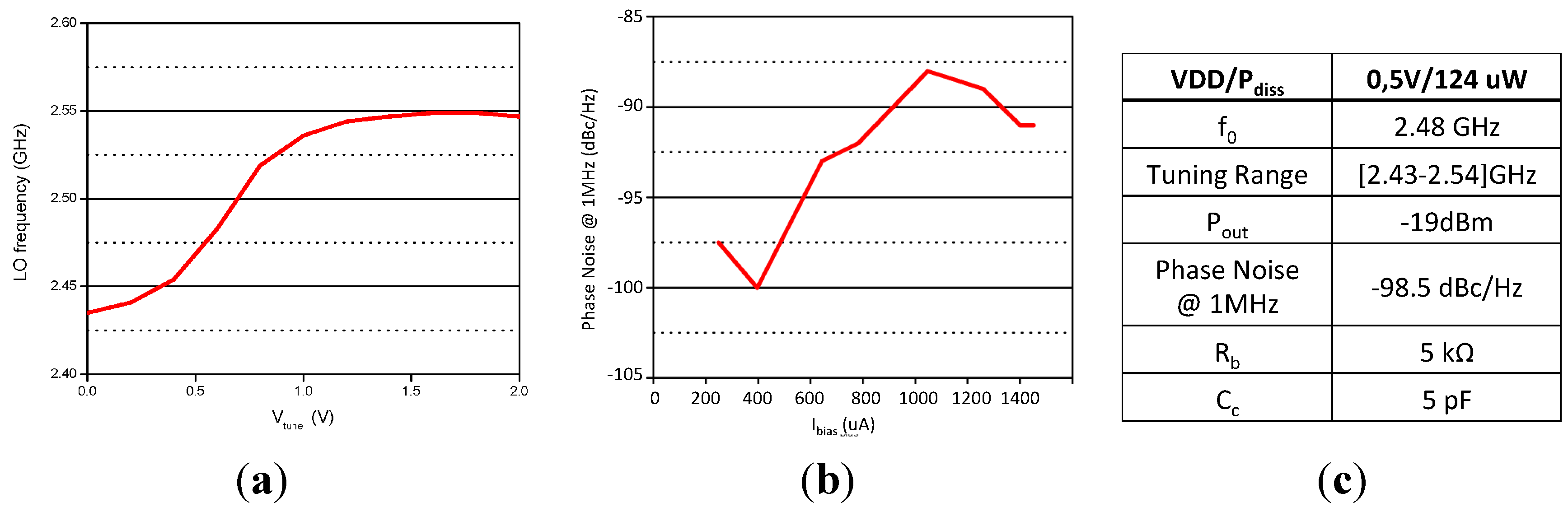
The tuning range of the oscillator is presented in
Figure 9a. The free running frequency is centered to 2.48 GHz, it can be adjusted from 2.43 GHz to 2.54 GHz. The phase noise (PN) is measured at 1 MHz from the carrier for different bias currents,
Figure 9b. A minimum PN of −100 dBc/Hz is achieved at 400uA. Below this value, the oscillator operates in current limited mode, the PN increases with the decrease of the current. Above 400 μA, the PN regrows as the oscillator operates in voltage limited mode. The oscillator is further exploited in a low power mode, and the bias current is fixed to 248 μA. The performances of the oscillator are reported in
Figure 9c for these conditions of operation.
Figure 9.
Oscillator Tuning Range versus Vtune (a); Phase Noise at 1MHz versus bias current (b) Oscillator performances at VDD = 0.5 V; & Ibias = 248 μA (c).
Figure 9.
Oscillator Tuning Range versus Vtune (a); Phase Noise at 1MHz versus bias current (b) Oscillator performances at VDD = 0.5 V; & Ibias = 248 μA (c).
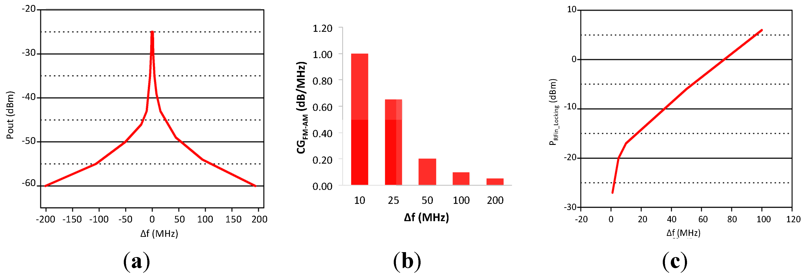
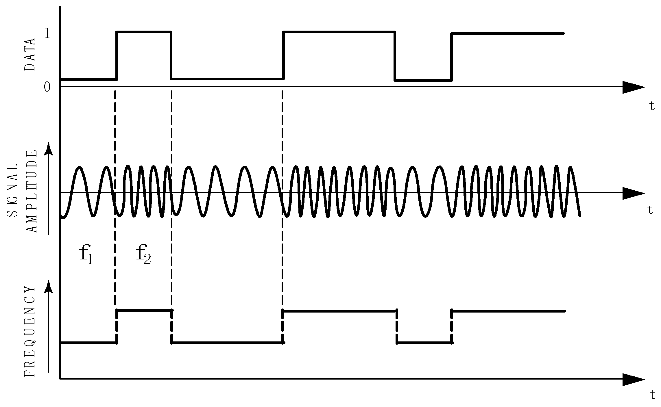
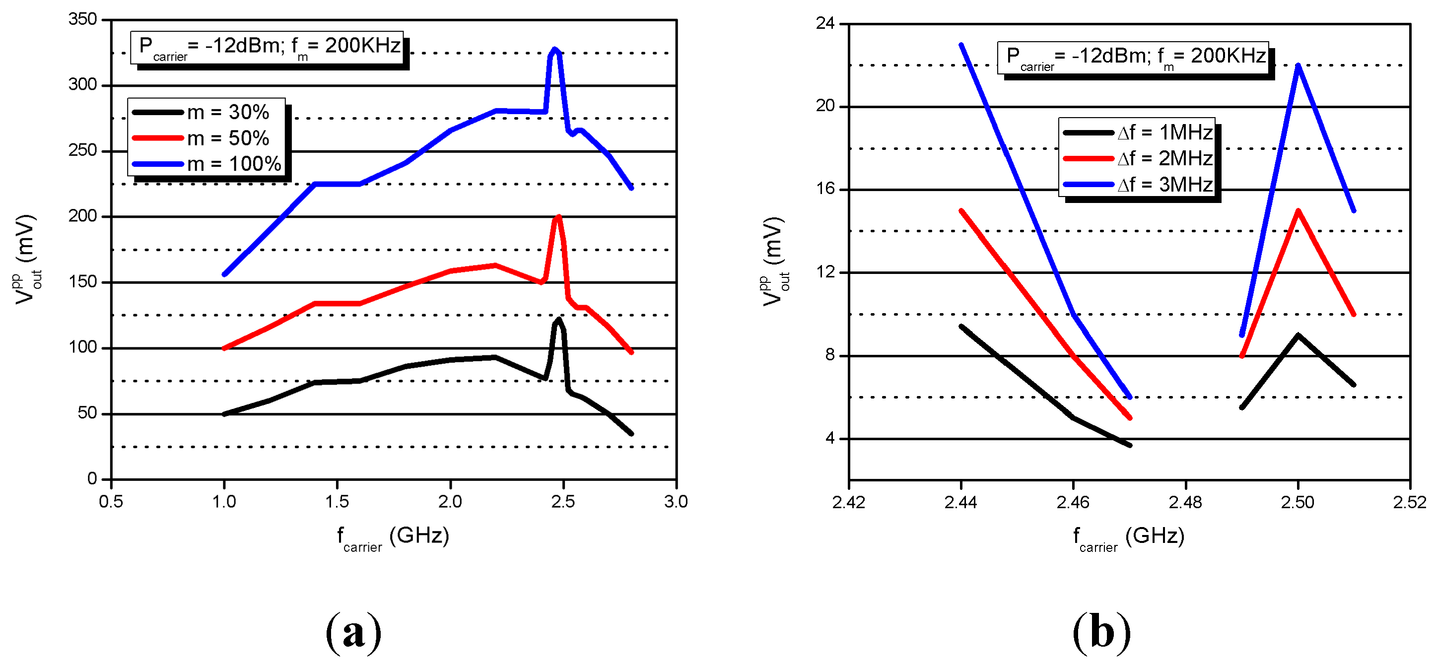
The two modes of operation, which will be further exploited in a MOOD receiver are pulled mode for FM to AM conversion and locked mode for AM to AM transfer. They are first characterized on the stand-alone 2.4 GHz LC-oscillator. To study the response in pulled mode, a continuous wave (CW) signal of −31 dBm is applied at the input node RF
in (
Figure 8a). The output power of the oscillator, P
out, is represented in
Figure 10a as a function of Δf, which is the deviation between the frequency of the CW signal and the free running frequency of the oscillator. For large frequency deviations, the output spectrum follows the free running response as it operates in pulled mode.
Figure 10b represents the maximum FM to AL conversion gain (CG
FM-AM) of the oscillator in pulled mode. The figures, extracted from
Figure 10a, are valid for a frequency shift of the FM signal equals to half of the corresponding frequency deviation Δf. CG
FM-AM strongly depends on the quality factor of the resonator, and it dramatically decreases when Δf exceeds 50 MHz. Within a frequency range of 2 MHz centered to the free running frequency, the oscillator is locked. The minimum power required to lock the oscillator is measured, and represented in
Figure 10b for different Δf. We can note the smaller the frequency deviation, the lower is the power required to lock the oscillator. At a Δf = 20 MHz, a minimum power of −15 dBm is needed to lock the oscillator, for larger frequency deviations the locking power linearly increases with Δf with a slope of 0.25 dB/MHz. This analysis figures out that the sensitivity of a MOOD demodulator operating in locking mode is improved when the free running frequency of the oscillator is tuned to the carrier frequency of the incoming AM signal.
Figure 10.
Pout in dBm versus Δf = |fLO − fRFin| with PRFin = −31 dBm & fLO = 2.48 GHz (a); FM to AM Conversion Gain (b); PRFin to lock the oscillator versus Δf = |fLO − fRFin| (c).
Figure 10.
Pout in dBm versus Δf = |fLO − fRFin| with PRFin = −31 dBm & fLO = 2.48 GHz (a); FM to AM Conversion Gain (b); PRFin to lock the oscillator versus Δf = |fLO − fRFin| (c).
3.2. Envelope Detector Design
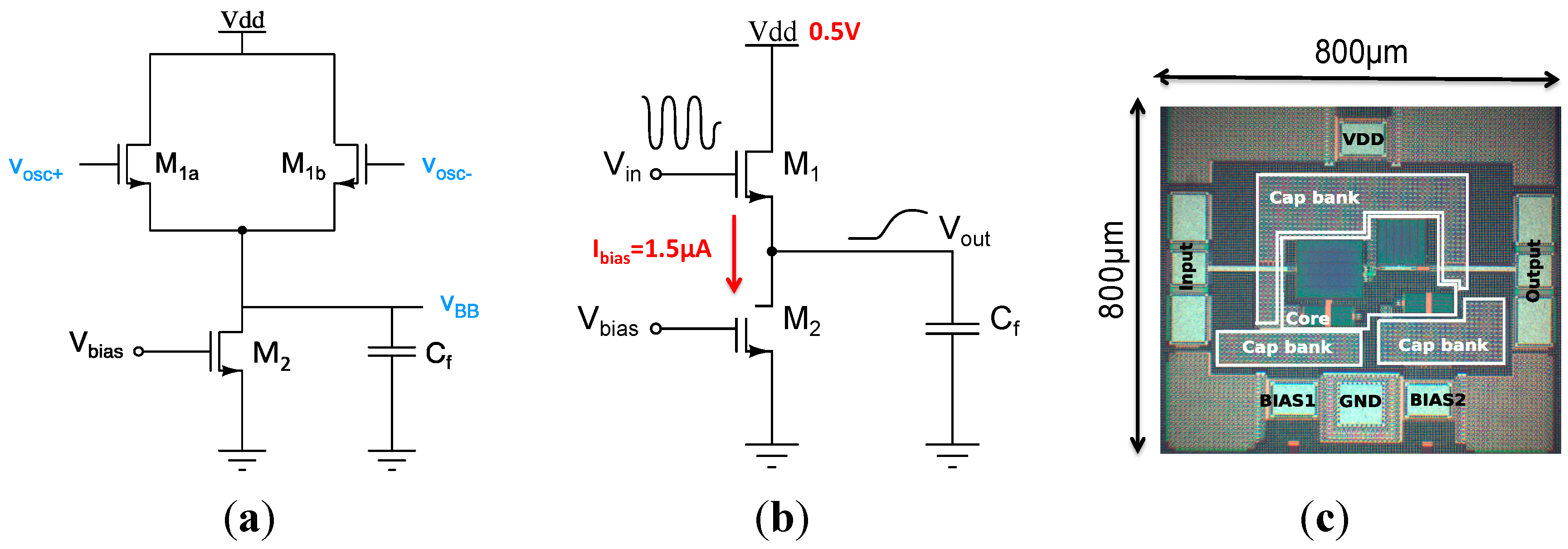
An envelope detector (ED) provides a simple and very low power solution to extract the data embedded in the amplitude of a signal. This detection circuit can be implemented using any non-linear element, such as a diode. However, in the CMOS process, it is convenient to use MOS transistors to perform the detection. The schematic of the envelope detector, included in the MOOD demodulator of
Figure 7, is presented in
Figure 11a. A single-ended version of the circuit,
Figure 11b,c, has been implemented for characterization.
The ED reported in
Figure 11 is a CMOS version of the standard bipolar topology described in [
13], and is basically a band-limited source follower. The operation of the circuit is similar to the bipolar version if the device M
1 is biased in weak inversion, as the drain current of a MOS transistor is an exponential function of gate-source voltage in this region. M
2 acts as a simple current source to bias M
1 with a constant current. A large capacitor C
f is connected to node V
out. The bandwidth at the output is derived in Equation (17). It is set by the pole f
p,det formed by C
f, and the output impedance of the detector which is approximately (1/g
m1) neglecting the body effect:
This pole is designed to be low enough to filter out any signal at the fundamental and higher harmonics but still affords enough bandwidth to avoid the attenuation of the baseband signal. For a typical OOK signal, the detected baseband waveform is a square wave, fp,det is adjusted to twice the maximum data rate of the demodulated signal.
Figure 11.
Differential ED implemented in the MOOD demodulator (a); single ED implemented as a standalone circuit for characterization (b); micrograph of the single ended ED in 65 nm CMOS (c).
Figure 11.
Differential ED implemented in the MOOD demodulator (a); single ED implemented as a standalone circuit for characterization (b); micrograph of the single ended ED in 65 nm CMOS (c).
An AC input signal is applied to the input, V
in in
Figure 11b. Since the output bandwidth is much smaller than the input signal frequency, the full signal appears across the gate-source terminal V
GS of M
1. M
1, biased in WI region, generates an output current that is an exponential function of the input voltage. To further investigate the circuit of
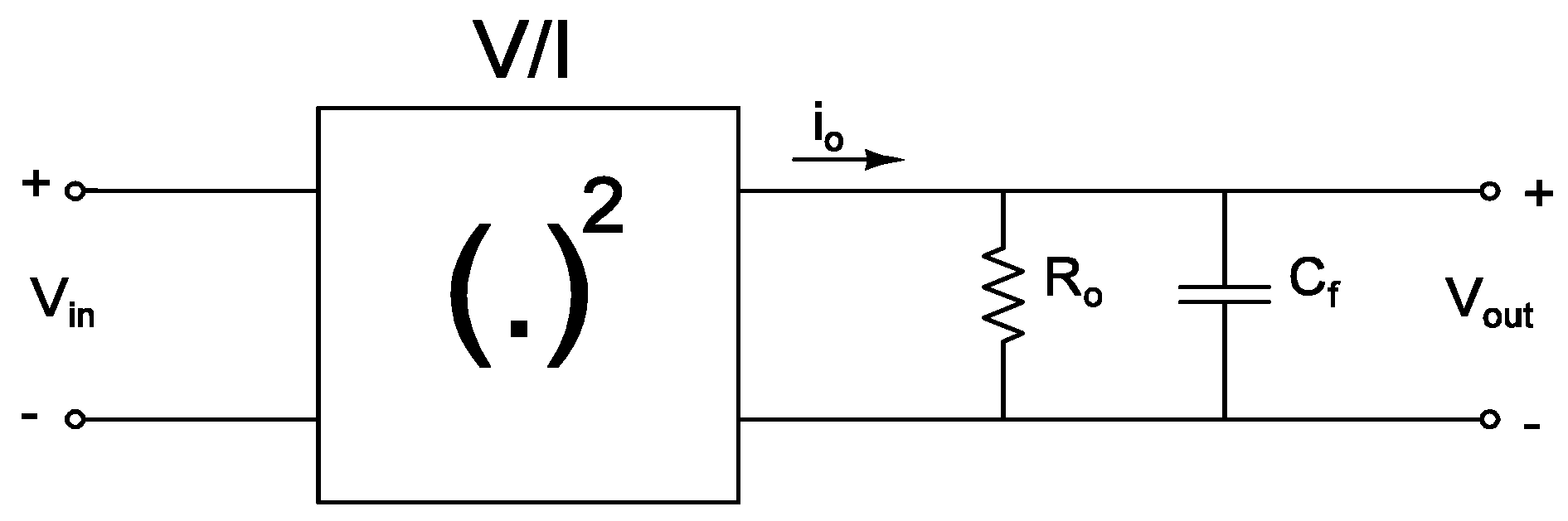
Figure 11b, an equivalent model is proposed in
Figure 12. The exponential function, expanded with Taylor series and dropping terms above the second order, acts as a squaring function. It actually transforms the AC amplitude of V
in into a DC current i
0. The fundamental frequency, along with higher order harmonics, of V
in will be filtered out by C
f. Although higher order terms will also generate DC components, these contributions are small compared to the squaring term. The output impedance R
o is simply 1/g
m1.
Figure 12.
Simple model of envelope detector to calculate conversion gain.
Figure 12.
Simple model of envelope detector to calculate conversion gain.
Referring to
Figure 11b, the large signal drain current of M
1 operating in weak inversion is modeled as [
14]:
where I’
0 is a constant depending on process and device size, V
th is the threshold voltage, V
t is the thermal voltage (kT/q), and n is the subthreshold slope factor. Expanding Equation (18) in Taylor series and focusing on the second order term, the DC component i
0 of I
D is expressed in Equation (19):
Substituting for V
in, the expression of a sine wave (V
s sin(ω
st)) with g
m = I
D/nV
t, the DC component i
0,
Figure 17, becomes:
The second harmonic term in Equation (20) is filtered out by the detector output pole f
p,det, and the output voltage of the detector V
out is expressed as Equation (21):
The conversion gain of the detector, GC
det, is finally the ratio of the output DC voltage V
out to the peak AC amplitude V
s of V
in:
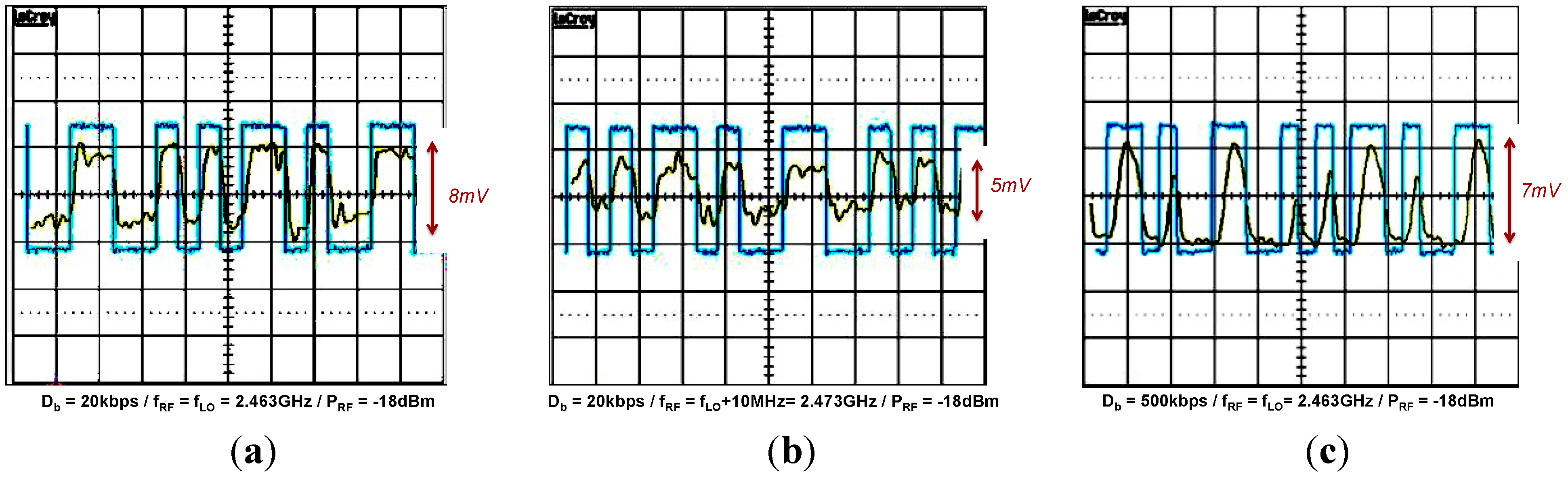
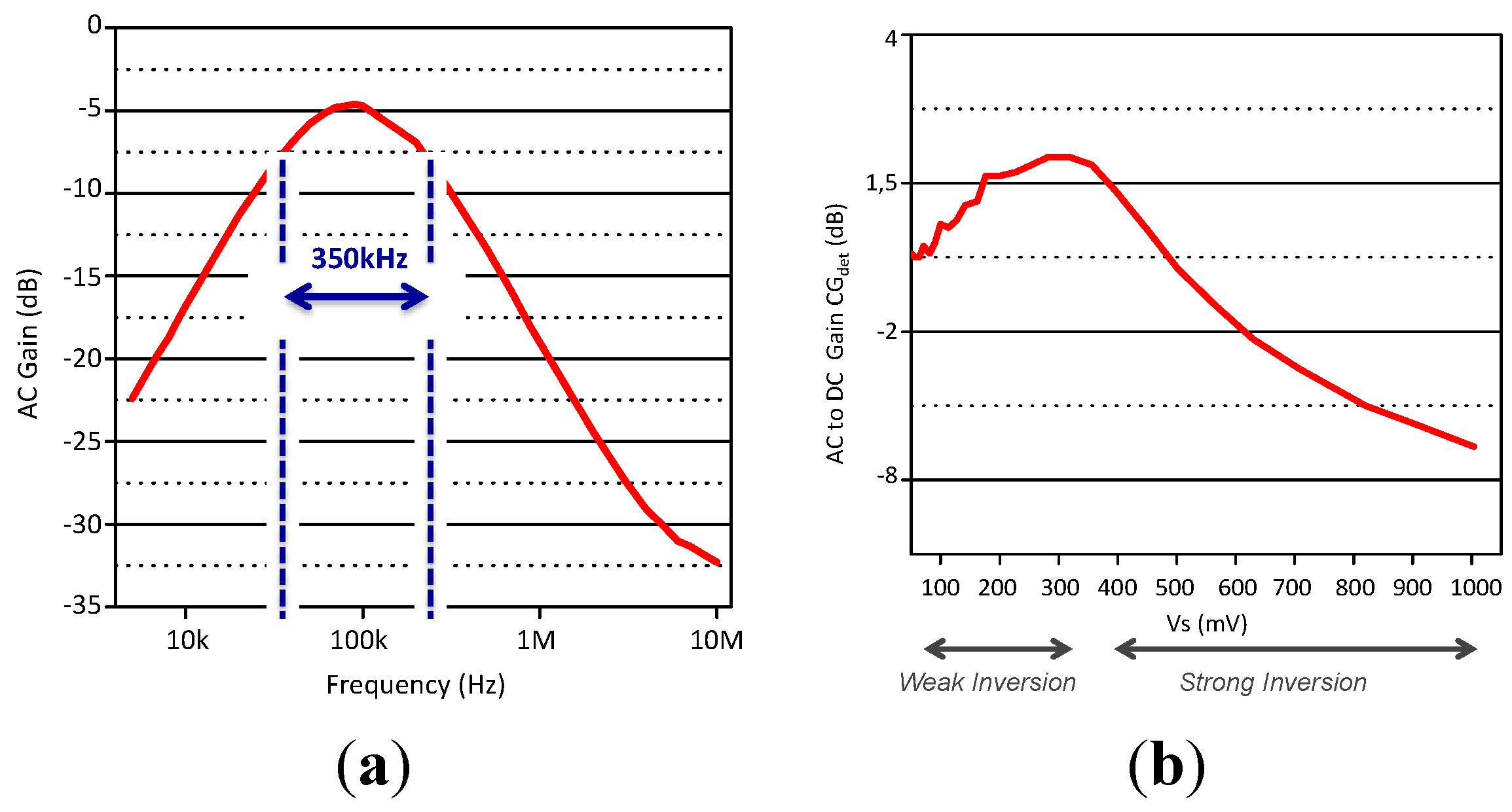
The measurement results of the single-ended detector are reported in
Figure 13. The circuit consumes 2 μW for a VDD of 0.5 V. The frequency response of the detector,
Figure 13a, exhibits a −3 dB bandwidth of 350 kHz, which allows a data rate demodulation up to 200 kb/s. According to Equation (22), the RF to DC conversion gain is a function of the input signal amplitude V
s. This analysis holds for small input signals where the response is dominated by the second order term and higher order effects are not significant. The measured conversion gain, GC
det, is illustrated in
Figure 13b. If the amplitude of the input signal is kept below 200 mV, GC
det is close to 0dB and the expression (Equation (22)) gives a good approximation of it. If the amplitude is larger than 400 mV the conversion gain rolls off, and the small signal analysis is no longer correct. To preserve the dynamic of demodulated data, the amplitude of the AM signal at the input of envelope detector would not exceed 500 mV.
Figure 13.
AC gain (a); AC to DC conversion gain CGdet versus the input amplitude Vs (b) of the envelope detector.
Figure 13.
AC gain (a); AC to DC conversion gain CGdet versus the input amplitude Vs (b) of the envelope detector.


