Review

Study of Back Biasing Schemes for ULV Logic from the Gate Level to the IP Level

ICTEAM institute, Université catholique de Louvain, Place du Levant 3, 1348 Louvain-la-Neuve, Belgium
*
Author to whom correspondence should be addressed.
J. Low Power Electron. Appl. 2014, 4(3), 168-187; https://doi.org/10.3390/jlpea4030168
Submission received: 14 March 2014 / Revised: 20 June 2014 / Accepted: 27 June 2014 / Published: 7 July 2014
(This article belongs to the Special Issue Selected Papers from IEEE S3S Conference 2013)

Abstract

:
Minimum energy per operation is typically achieved in the subthreshold region where low speed and low robustness are two challenging problems. This paper studies the impact of back biasing (BB) schemes on these features for 28 nm FDSOI technology at three levels of abstraction: gate, library and IP. We show that forward BB (FBB) can help cover a wider design space in terms of the optimal frequency of operation while keeping minimum energy. Asymmetric BB between NMOS and PMOS can mitigate the effect of systematic mismatch on the minimum energy point (MEP) and robustness. With optimal asymmetric BB, we achieve either a MEP reduction up to 18 % or a 36× speedup at the MEP. At the IP level, we confirm the MEP configurability with BB with synthesis results of microcontrollers at 0.35 V. We show that the use of a mix of overdrive FBB voltages further improves the energy efficiency. Compared to bulk 65 nm CMOS, we were able in 28 nm FDSOI to reduce the energy per cycle by 64 % or to increase the frequency of operation by 7×, while maintaining energy per operation below 3 μW/MHz over a wide frequency range.

1. Introduction

With the accelerating expansion of ultra-low-power computing and energy-autonomous systems requested by the vision of the Internet-of-Things, the need for compact battery-less wireless sensor nodes with consequent embedded data processing abilities is getting stronger [1]. In these systems, energy sobriety supersedes the traditional hunt for speed performances, and the Ultra Low Voltage operation region has became a hot topic in low-power research. As introduced in [2] and modeled in [3], energy minimization due to the tradeoff between leakage energy and switching energy is achieved in the subthreshold domain, as shown in Figure 1. Operating with such an aggressively scaled down supply voltage ( V D D ) can lead to energy savings up to 10 × [4]. As shown in [5], subthreshold FDSOI circuits are emerging and can lead to very high energy efficiency. However, this scaling is limited by two factors: the target frequency constraint and the robustness constraint [6]. In order to meet the target frequency of the application, the V D D may need to be raised above the optimal energy point. Below the threshold voltage ( V T ), the I O N / I O F F ratio of MOSFET exponentially exacerbates the sensitivity to random variation and increasing functional failure probability [7]. A thorough examination of the design techniques that can be used in ULV to mitigate such constraints can be found in [8].
Figure 1. Optimal E c y c l e and minimal V D D to achieve a target clock frequency in 28 nm FDSOI regular V T (RVT) and low V T (LVT) devices from Figure 2. Simulation results for an eight-bit multiplier using the ELDO simulator from Mentor and 28-nm FDSOI CMOS models from STMicroelectronics. We estimated the 3σ worst-case delay obtained though 1 k Monte-Carlo (MC) simulations, and the robustness limit is extracted from 80 k MC simulations following the framework detailed in [6].
Jlpea 04 00168 g001
In this work, we explore the potential of back biasing technique in FDSOI technology to mitigate both constraints. Back biasing (BB) voltage controls the V T through the back gate and can be used to dynamically adapt V T in operation. The impact of back gate voltage biasing on V T is detailed in Section 2. As the minimum energy point and the frequency of operation of the minimum energy point (MEP) ( f M E P ) are linked to the threshold voltage [9], dynamic V T can help keep a circuit with variating computational workload near an energetic optimum. Figure 1 shows how the MEP is shifted toward higher operating frequencies between regular V T (RVT) and low V T (LVT) devices in the 28-nm FDSOI high-κ/metal-gate CMOS technology from STMicroelectronics [10].
Figure 2. Schematic view of RVT and LVT devices in 28-nm Ultra Thin Body and BOX FDSOI technology from STMicroelectronics. Back biasing voltages for: (top) RVT devices that are similar to bulk technologies; (bottom) LVT devices implemented with a flip well.
Jlpea 04 00168 g002
We study the impact of V T modulation through BB on three abstraction levels:
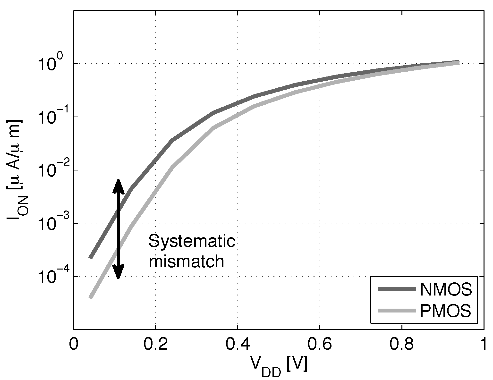
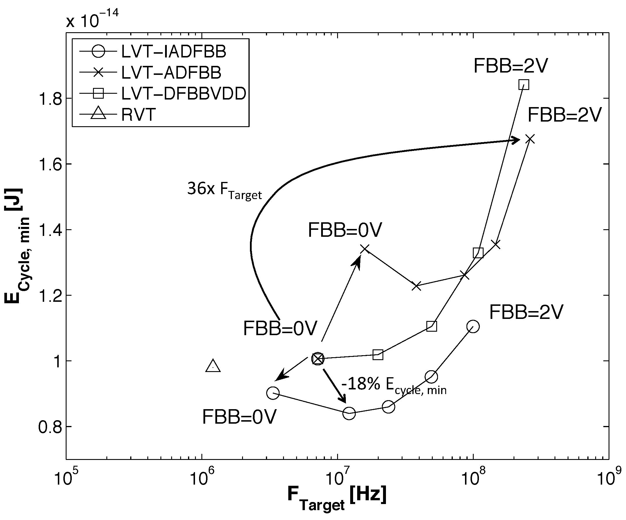
  • At the gate level, we evaluate the impact of back gate biasing and several schemes of back gate biasing on key factor of merit of a test bench circuit simulated at gate level. Technology scaling of bulk CMOS leads to increased variability, drain-induced barrier lowering (DIBL) and gate leakage that are harmful to the minimum energy level [9]. MEP reduction with technology scaling is limited by short channel effects in advanced bulk nodes, calling for FDSOI technologies to keep reducing MEP, while improving the corresponding f M E P . In this work, the 28-nm FDSOI technology MEP is compared to 130-nm to 28-nm bulk technology MEP to quantify the high potential of FDSOI for ultra-low power and ultra-low voltage anticipated in [11,12,13]. Section 3.1 illustrates the effect of scaling and back biasing in the ULV domain. In addition to its use for trading the performance for energy efficiency, body biasing has already been proposed on bulk technology to mitigate random V T mismatch under process variation (PV) in [14]. In [15], the authors proposed an analytical framework to analyze the PMOS/NMOS ratio variation with supply voltage and an adaptive scheme to optimize this ratio while compensating for PV. In this work, we use BB to control systematic PMOS/NMOS mismatch over the V D D range without resorting to sizing modifications, allowing the use of standard cell libraries sized at nominal voltage. Systematic mismatch cancellation results in both energy and robustness improvement. We show that such adaptive BB can save 18 % of energy per cycle at MEP and improve the gate count for a 95 % functional die yield by a factor of six. Mismatch compensation schemes are described in Section 3.2, and energy efficiency and robustness results are shown in Section 3.3 and Section 3.4;
  • At the library level, we recharacterized a standard cell library when applying different BB voltages and investigate the obtained performances, as shown in Section 4;
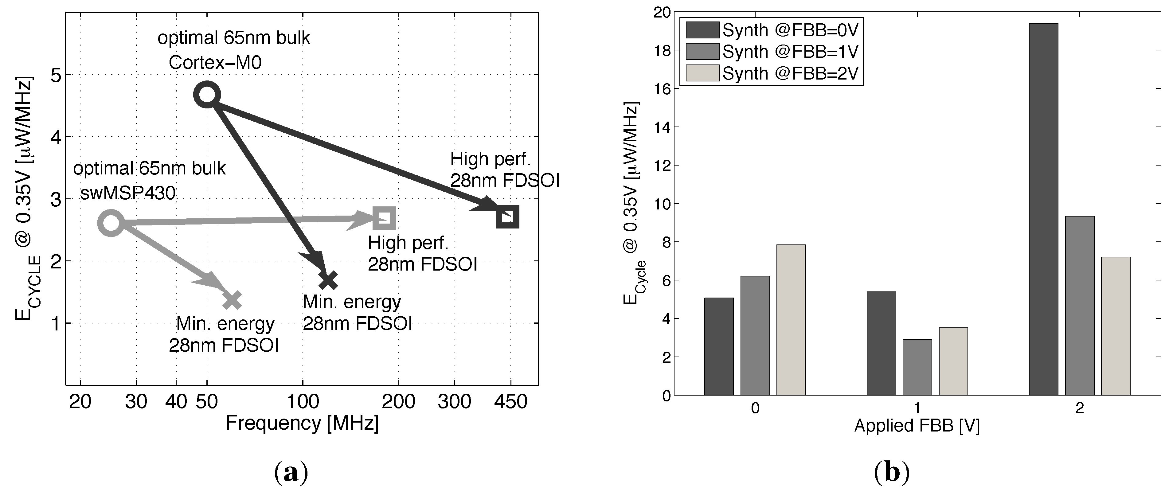
  • At the IP level, we study the scaling perspective of ULV microcontrollers cores towards a 28-nm implementation by using the recharacterized libraries. We validate the conclusions made at the gate and library levels based on the synthesis results of two microcontroller cores at 0.35 V in 28 nm FDSOI, as compared to the latest best-in-class results in 65-nm CMOS bulk [4]. Energy efficiency depending on BB use at the synthesis or during the operation of the microcontroller is discussed in Section 5.
This work consists of a collection of previously published results on forward BB (FBB) impact at the gate level [16] and at the IP level [17]. Section 2 and Section 4 contain unpublished results, from which we are able to extract a coherent view of BB in FDSOI circuits from the device to synthesized IPs.

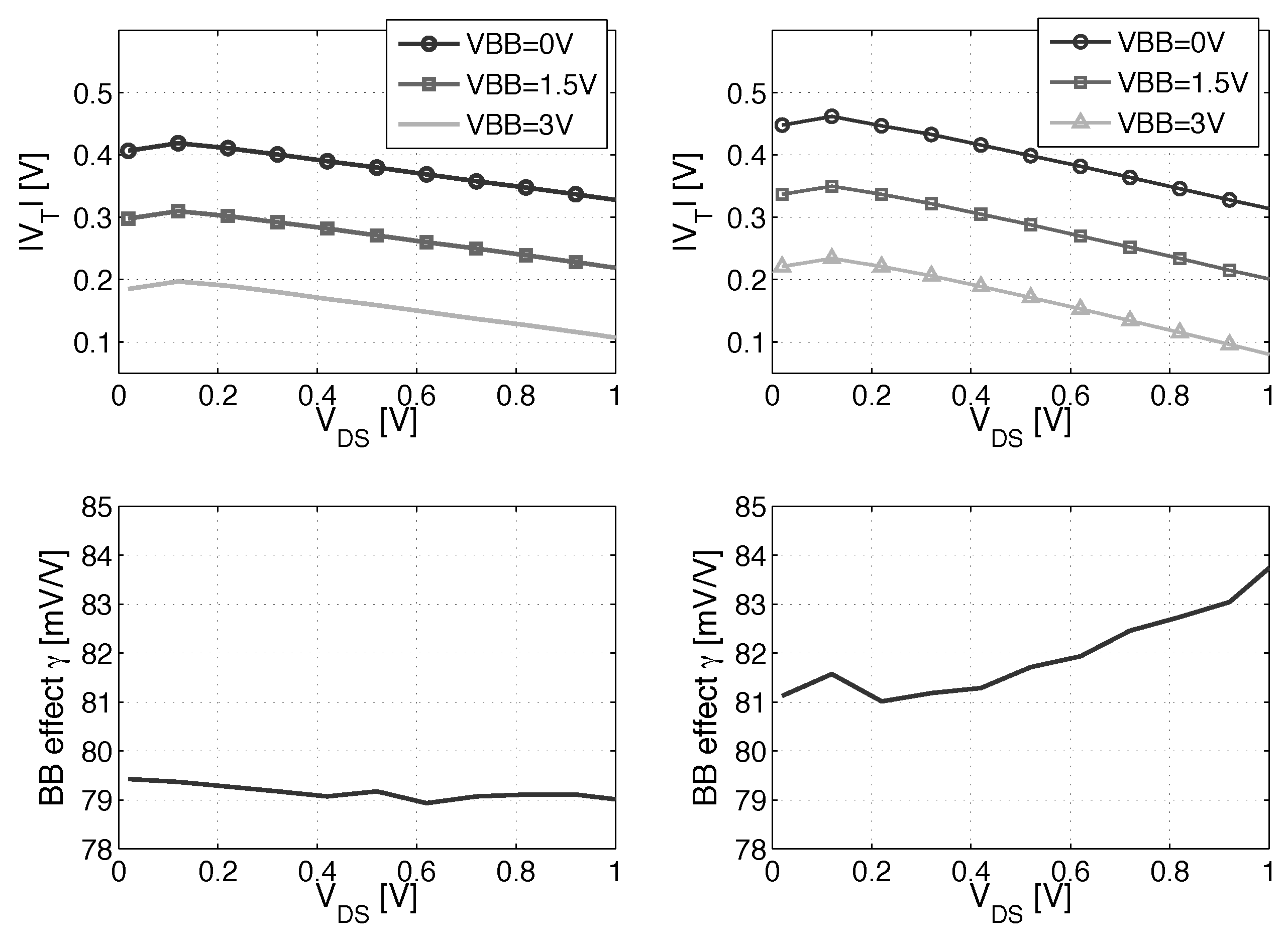
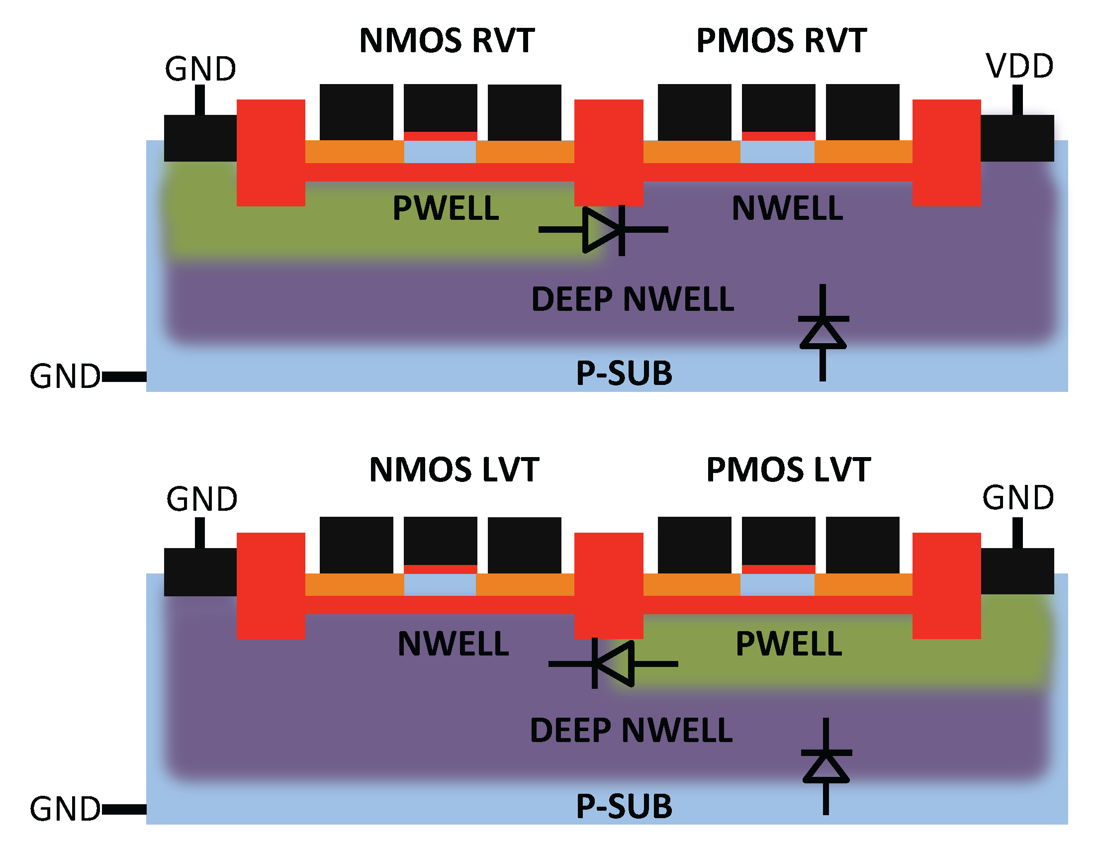
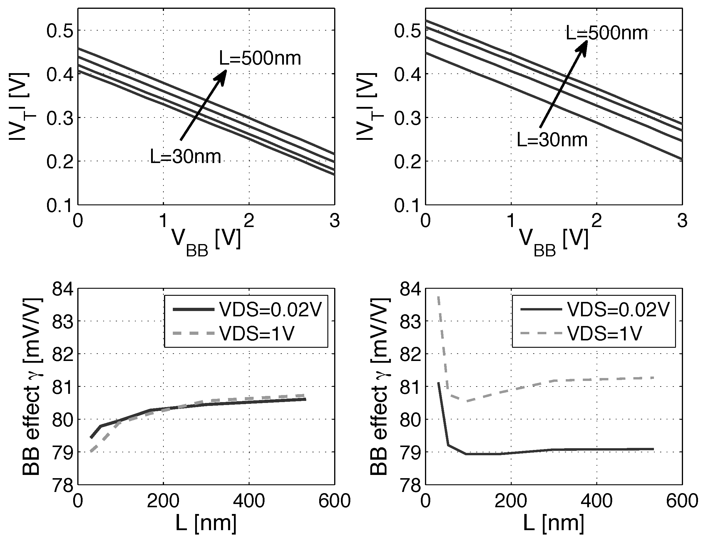
2. Back Biasing at the Device Level

The V T modulation through back gate biasing can be modeled as follows [18]:
V T = V T 0 - γ × V B S
with γ, the back gate effect taking into account the electrostatic control of the back gate over the channel, and V B S , the back gate biasing voltage.
Figure 3 shows the absolute value of the V T for NMOS and PMOS LVT devices implemented using flipped well structures (cf. Figure 2). The V T value drops with the forward BB down to 0.2 V at FBB = 3 V. Increasing the length of the devices increases the V T for all FBB voltage, due to DIBL and V T roll-off mitigation at a long channel length.
Figure 3. The impact of back biasing (BB) on V T for a gate length from 30 to 500 nm. (Left) NMOS LVT device; (right) PMOS LVT device.
Jlpea 04 00168 g003
The γ parameter evolution with the length is also featured in Figure 3. For NMOS, γ is mostly independent of L g , but the PMOS device shows a slightly higher variation with L, but also with V D S , especially for a short gate length. This suggests that even for a long channel length, the DIBL of the PMOS is significant. We can reduce the V T and improve γ for the PMOS by using a minimum gate length device. Lower V T is interesting for high-speed ULV circuits in order to improve the I O N current, as shown in Section 3.2, and a higher γ improves the efficiency of all of the back biasing schemes for performance tuning presented in this work. In particular, short channel PMOS presents a lower systematic V T mismatch with the NMOS, hence improving the speed and robustness, as shown in Section 3.3 and Section 3.4.
Figure 4 shows that the V T is maximum at V D S = 0.1 V. In ULV circuits with V D D down to ≈0.3 V, the high V T results in lower I O N . The γ coefficient variation with V D S is higher for the PMOS due to the higher DIBL.
Figure 4. V T and γ coefficient for three FBB voltages depending on V D S . (Left) NMOS LVT device; (right) PMOS LVT device.
Jlpea 04 00168 g004

3. Back Biasing Analysis at the Gate Level

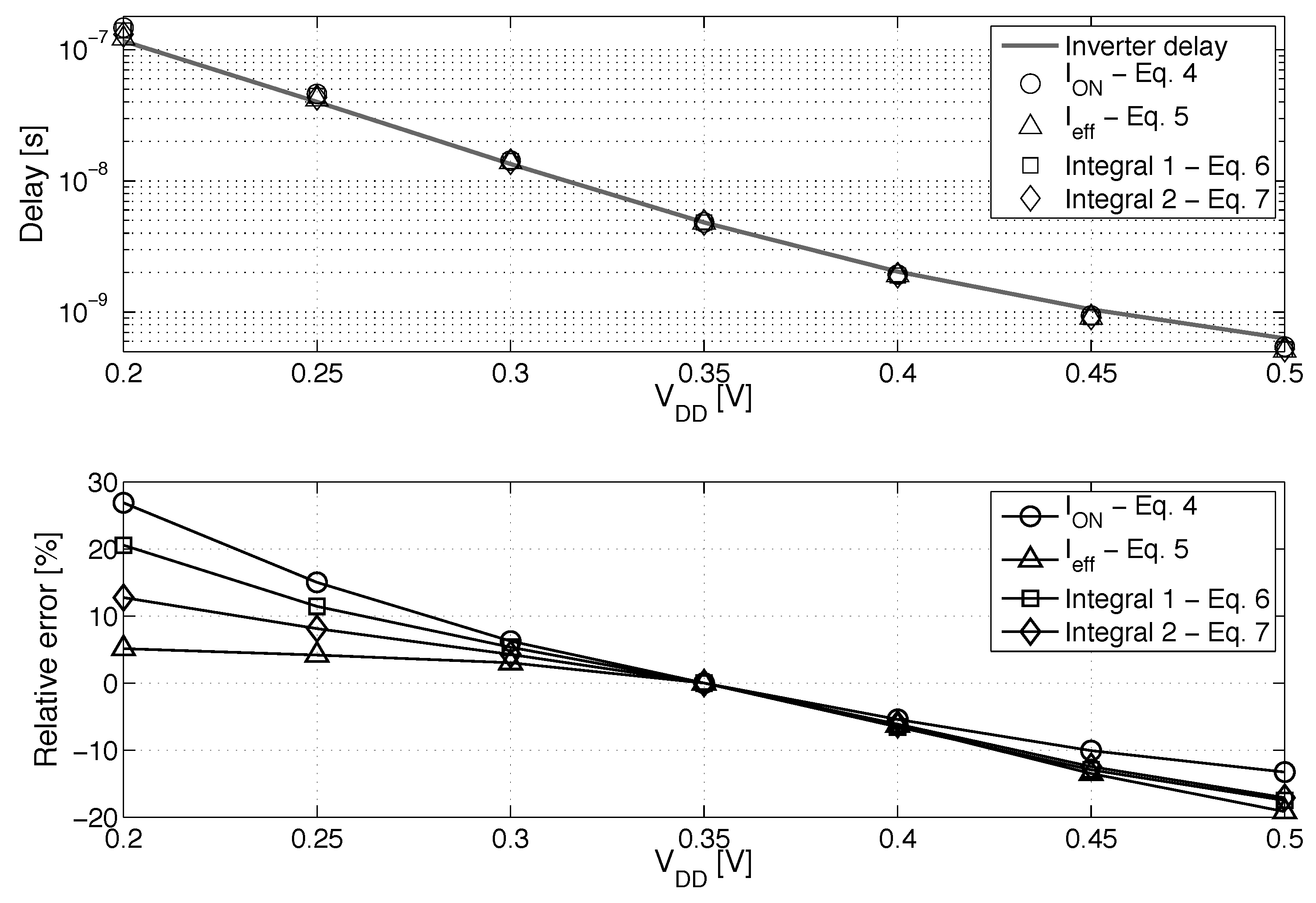
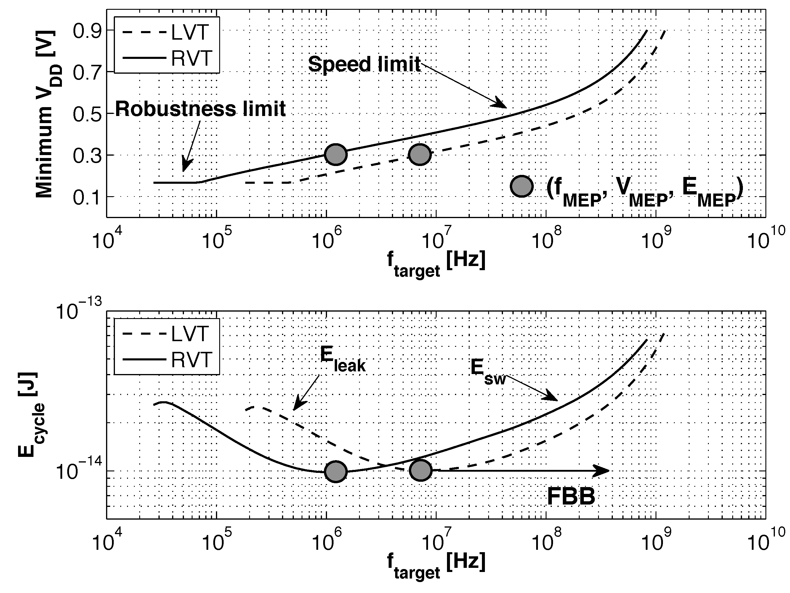
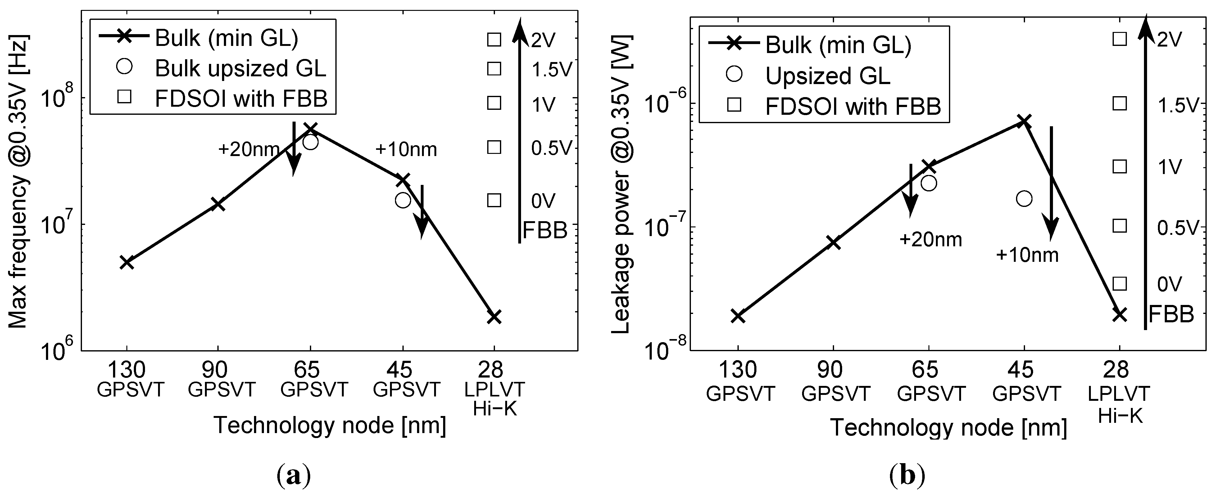
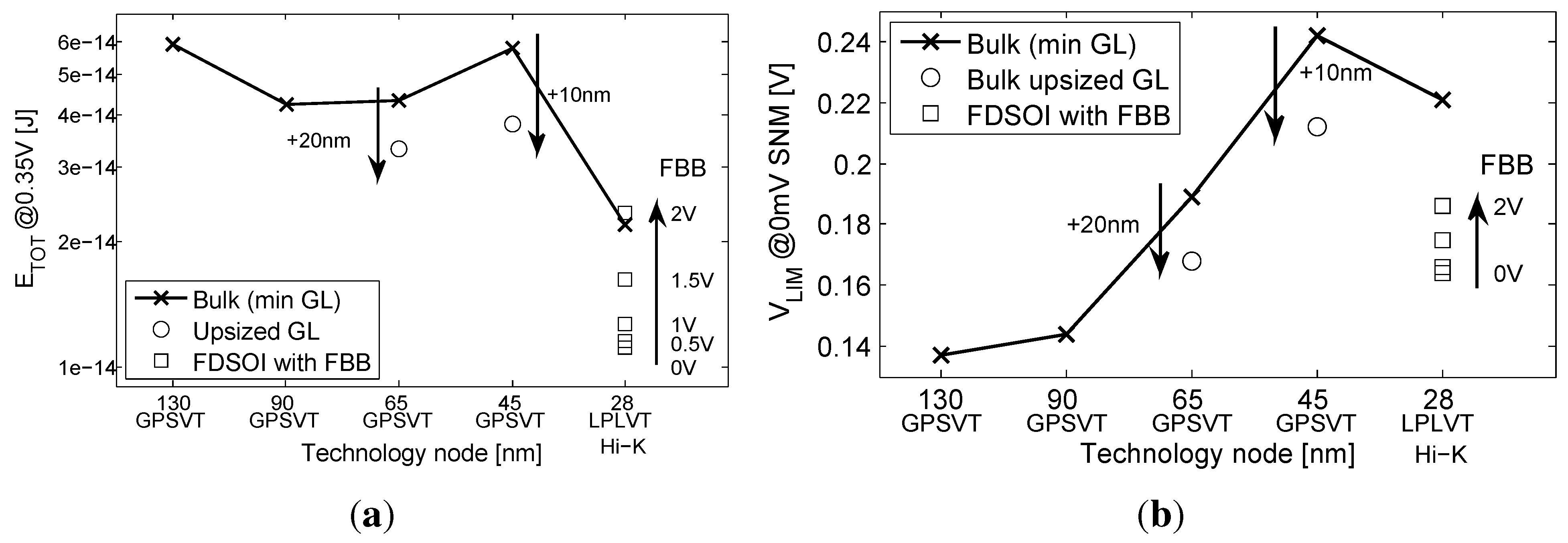
3.1. Scaling and Back Biasing Impact on Frequency and Energy Efficiency

To study the evolution of relevant figures-of-merit (FoMs) for circuit design with scaling, we simulated in SPICE an eight-bit benchmark multiplier at 0.35 V from 0.13 μm to 28 nm. We only considered LVT MOSFETs in 28 nm FDSOI for speed concerns and considered different FBB voltages applied to FDSOI (overdrive FBB voltages up to 2 V). In the 65/45-nm bulk, we used upsized gate length (GL) to improve the energy efficiency and functional robustness [6,9].
Figure 5 and Figure 6 shows SPICE simulations of an eight-bit benchmark multiplier at 0.35 V in 130-nm, 90-nm, 65-nm and 45-nm bulk with a GP CMOS process (SVT MOSFETs) and in a 28-nm node with an LP CMOS process, as offered by the foundry, both in bulk and FDSOI technologies, following the framework used in [6,9]. Upsized-GL devices were upsized by 20 nm in 65 nm and by 10 nm in 45 nm. Signa to Noise Margins (SNMs) were simulated as proposed in [7] based on 80 k Monte-Carlo simulations of cross-coupled NAND2-NOR2 gates, and the V L I M I T is defined as the minimum V D D , allowing a 0 . 1 % negative noise margin.
Figure 5. The evolution of the (a) maximum frequency of operation and (b) static power consumption with scaling in the ULV domain.
Jlpea 04 00168 g005
Figure 6. The evolution of (a) energy per operation and (b) robustness with scaling in the ULV domain.
Jlpea 04 00168 g006
As shown on Figure 5a, the maximum frequency increases between 0.13 μm and 65 nm as a result of the reduction in node capacitance and the V T value. As predicted in [19], the 45-nm node is slower than the 65-nm one. There are three factors in play in this speed reduction: a saturation of the typical subthreshold I O N current [19], a significant increase of the ion variability [19] and an NMOS/PMOS systematic mismatch. These three factors cause a 3 σ worst case delay increase, observed in Figure 5a.
The 28-nm bulk implementation is slower than any other bulk nodes, due to the LP CMOS process. Using FBB to reduce the threshold voltage can provide a speed up as high as 17× between a 0-V bias and a 2-V bias. Figure 5b shows the same trend for the leakage power (from both drain and gate leakages). The leakage of the 28-nm bulk is reduced by a factor 35× compared to the 45-nm one, thanks to the LP CMOS process and the high-κ/metal gate. The FBB on FDSOI greatly increases the leakage through the V T reduction. The total E C Y C L E shown in Figure 6a is degraded from 90 to 45 nm, illustrating the energy overhead of short channel effects, variability and gate leakage [9]. Upsized-GL at 65/45 nm improves the total E C Y C L E at the expense of a 25 / 45 % speed penalty. The 28-nm technology shows outstanding results in E C Y C L E , especially in FDSOI, thanks to the high-κ/metal gate and to the lower short channel effects and, thus, reduced DIBL. Figure 6b further illustrates the degradation of functional robustness at ULV through the evolution of V L I M I T with scaling. As predicted, the low variability due to the undoped channel and the low short-channel effects of FDSOI restores functional robustness at 28 nm by improving V L I M I T .
Based on these results, we can discard the 28-nm bulk technology, as it will be too slow to implement ULV circuits in the MHz range and as it features a robustness limit close to the targeted supply voltage. Contrary to 28-nm bulk, FDSOI technology allows high-speed operation and high robustness at 0.35 V.

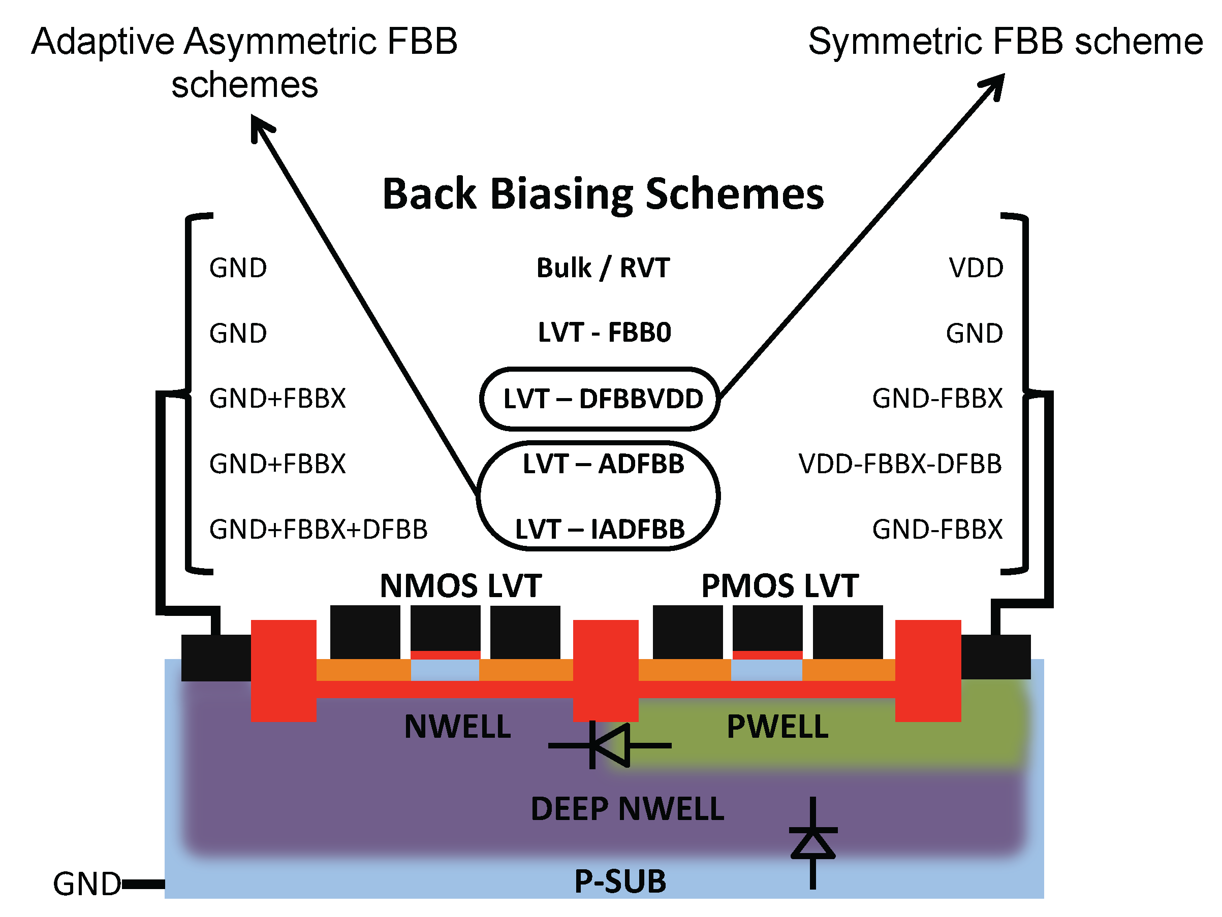
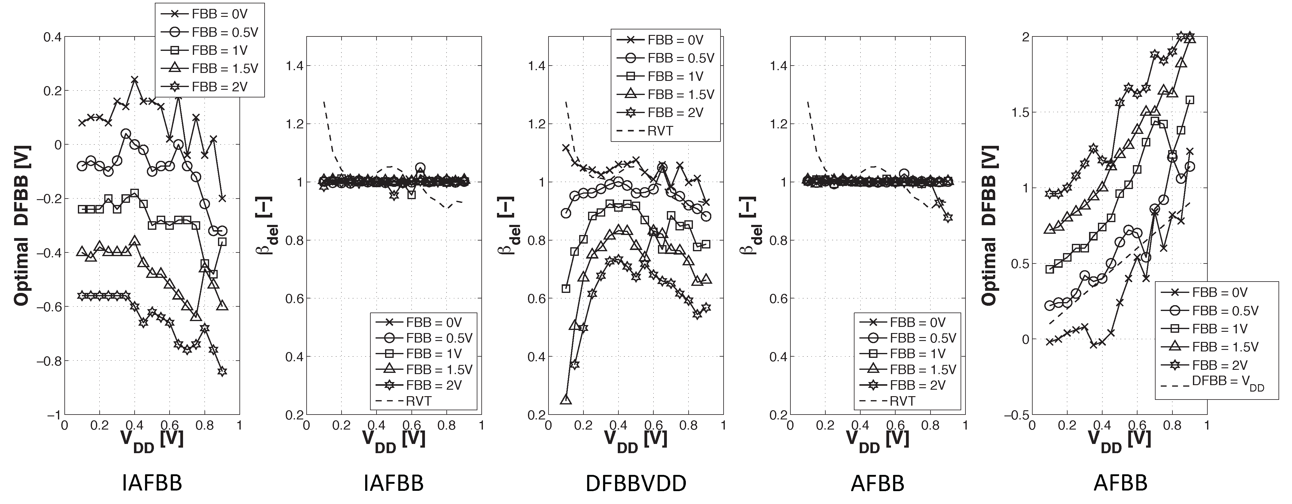
3.2. Delay Equalization and Back Biasing Compensation Schemes

Body biasing has already been proposed for bulk technology to mitigate random V T mismatch under process variation (PV) in [14]. In [15], the authors proposed an analytical framework to analyze the PMOS/NMOS ratio variation with supply voltage and an adaptive scheme to optimize this ratio while compensating for PV. In this work, we use BB to control systematic PMOS/NMOS mismatch over the V D D range without resorting to sizing modifications, allowing the use of standard cell libraries sized at nominal voltage. We show that such adaptive BB can save 18 % of the energy per cycle at MEP and improve the gate count for a 95 % functional die yield by a factor of six.
To examine the impact of the PMOS/NMOS ratio variation on the relevant FoMs, we model the subthreshold delay and leakage power. In the subthreshold regime, the drain current can be expressed as in [18]:
I D , s u b = I 0 × 10 V G S - η V D S S × ( 1 - e - V D S U t h )
with U t h , the thermal voltage, S, the subthreshold swing, and η, the modeling DIBL effect. I 0 regroups the threshold voltage variation due to back gate voltage V B S and bias-independent factors, particularly the body factor n and the zero-bias threshold voltage V T 0 :
I 0 = μ 0 C o x 1 L e f f ( n - 1 ) U t h 2 10 - V T 0 + γ V B S S
The NMOS and PMOS I O N are matched at nominal V D D by upsizing the PMOS, but a mismatch appears in the subthreshold domain and for varying BB as the drive current becomes exponentially dependent on the threshold voltage. Figure 7 shows a divergence between NMOS and PMOS I O N below 0.4 V.
There are several ways to modelize the gate delay based on IdVd simulations. We compared four modelizations expressed in Equations (4)–(7).
T d e l , i n v C V D D m e a n ( I O N , N , I O N , P )
T d e l , i n v C V D D m e a n ( I e f f , N , I e f f , P )
T d e l , i n v C V D D 2 m e a n ( 0 V D D I D , N @ V G S = V D D d V D S , 0 V D D I D , P @ V G S = V D D d V D S )
(7) T d e l , i n v C V D D m e a n ( α N , α P ) with α = 1 2 0 V D D I D @ V G S = V D D d V D S + 1 2 0 V D D I D @ V G S = V D D / 2 d V D S
Figure 7. NMOS and PMOS I O N evolution with V D D for LVT MOSFET with FBB = 2 V ( W p = 160 nm, W n = 80 nm, L p = L n = 30 nm and V D S = V G S = V D D , V B S = G N D ). The PMOS BB is connected to GND . Simulation results are obtained with the ELDO simulator and 28-nm FDSOI CMOS models from STMicroelectronics.
Jlpea 04 00168 g007
Equation (4) is based on the ON current and Equation (5) is based on the effective current first defined in [20] as:
I e f f = 1 2 { I D ( V G = V D D / 2 ; V D = V D D ) + I D ( V G = V D D ; V D = V D D / 2 ) }
Equations (6) and (7) are based on the integration of the IdVd curve at V G = V D D or at V G = V D D / 2 . Figure 8 shows the modelization error compared to the simulated delay of an FO1 inverter chain depending on V D D . The modelization based on the effective current produces good matching at ULV and, thus, is chosen to study the impact of systematic mismatch on energy efficiency.
The subthreshold leakage power can be expressed as:
P l e a k = I 0 10 η V D D S × V D D
Based on the models in the subthreshold regime, we can study the impact of effective current mismatch on leakage energy. For an N-inverter chain, the total delay can be predicted as the product between the load capacitance and the mean effective current:
T d e l 2 × N × C l o a d × V D D ( I e f f , s u b , N M O S + I e f f , s u b , P M O S )
The total leakage current can be written as the arithmetic mean between the two devices’ leakage current:
P l e a k = N 2 ( I 0 , N 10 η N V D D S N + I 0 , P 10 η P V D D S P ) × V D D
Figure 8. Comparison between delay modelization from Equations (4)–(7) and the simulated delay of an FO1 inverter chain.
Jlpea 04 00168 g008
If the systematic mismatch ratio between the NMOS and PMOS effective current β I e f f = I e f f , N / I e f f , P is large, the delay can be, at best, divided by two, compared to a unitary ratio situation. The leakage current of the faster device will be increased, while the slower device leakage will be kept constant. The total leakage current will then increase by a factor N / 2 × β I l e a k ; with β I l e a k = I l e a k , N / I l e a k , P , the leakage current ratio between NMOS and PMOS. The leakage energy:
E l e a k = T d e l × I l e a k
will be increased by a factor N / 4 × β I l e a k that represents the E l e a k loss caused by device mismatch as β I l e a k is greater than one. A similar conclusion was drawn by Ono et al. [21] for PMOS/NMOS mismatch, due to local fluctuations.
PMOS and NMOS devices feature different I 0 , subthreshold swings and DIBL factors, which lead to larger than one β I e f f = I e f f , N / I e f f , P that is commonly corrected through upsizing PMOS devices targeting equal rising and falling inverter delays. Implementing subthreshold circuits with standard library cells implies the use of cells balanced at nominal V D D . Unfortunately, as the subthreshold I O N divergence suggests, the β I e f f ratio will diverge from its value at nominal V D D when the supply voltage is shrunk, leading to performance degradation. Figure 9 illustrates the validation of this theoretical trend by simulations and shows the β I e f f spreading in the subthreshold domain that will cause an E l e a k increase.
Based on these conclusions, we developed rise/fall delay mismatch compensation technique by using the wide range of BB as a new degree of freedom offered by FDSOI technologies. By variating the relative biasing between the NMOS and PMOS devices, we can use the back gate to modify the I 0 , N M O S / I 0 , P M O S ratio through the parameter γ in Equation (3) and control the effective current mismatch.
Figure 9. NMOS-PMOS I e f f ratio evolution with V D D for RVT MOSFET and LVT MOSFET with different FBB voltages ( W p = W n = 80 nm, L p = L n = 30 nm). The PMOS BB is connected to GND . Simulation results are obtained with ELDO simulator and 28-nm FDSOI CMOS models from STMicroelectronics.
Jlpea 04 00168 g009
In order to study the back biasing potential in the subthreshold domain, we selected five levels of forward back biasing to be applied on the LVT device: from 0 V up to 2 V. In addition to the FBB, three adaptive asymmetric delta forward back biasing (DFBB) schemes, illustrated in Figure 10, were investigated:
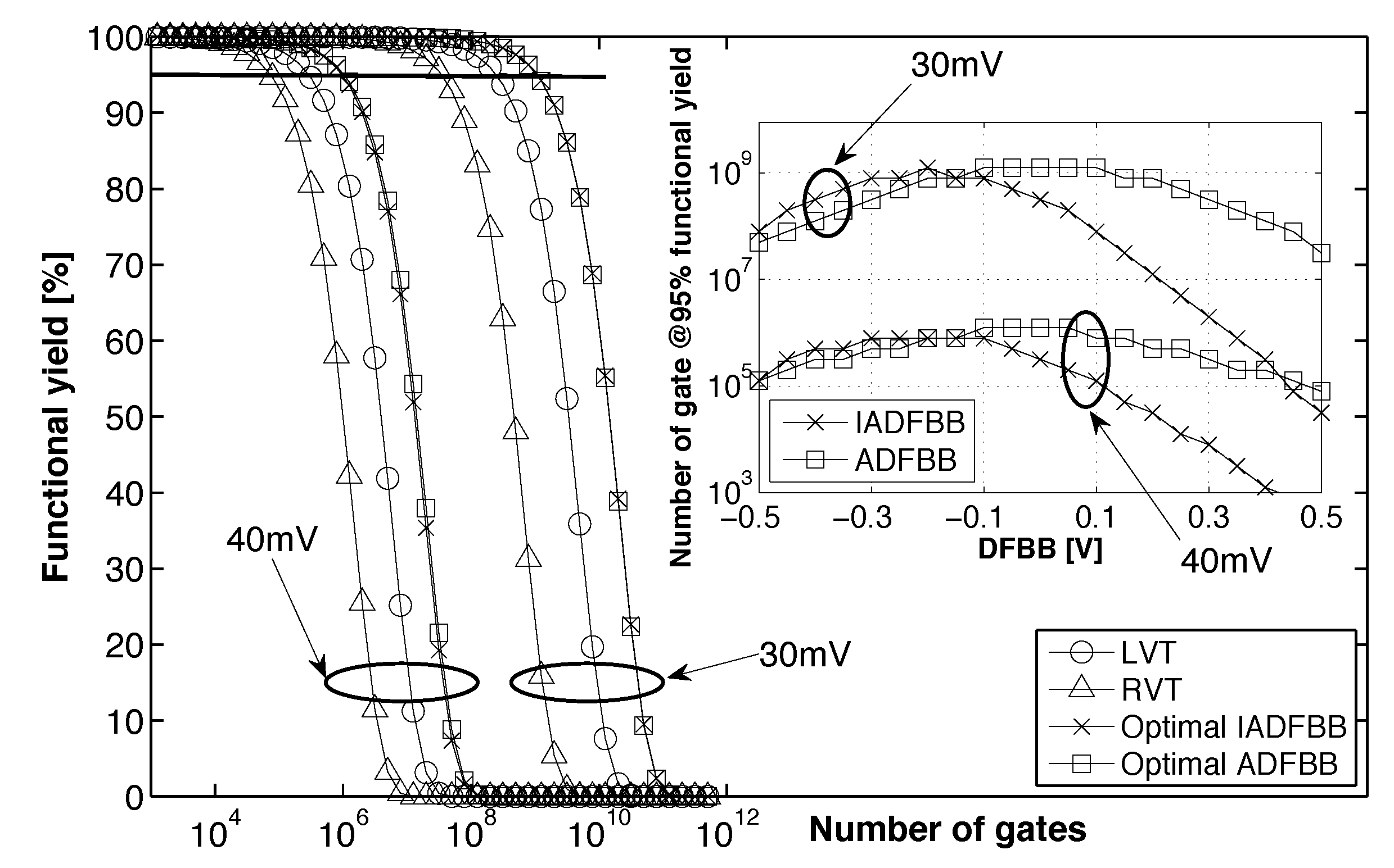
  • DFBBVDD: The PMOS back gate is connected to GND instead of V D D , as in bulk technology or for RVT devices. The DFBB is equal to V D D (DFBBVDD). In this technology, the PMOS is weaker than the NMOS, and a straightforward way to roughly compensate for the systematic mismatch is to apply a differential FBB equal to the nominal V D D 0.9 − 1 V on the PMOS. This scheme is a simple extrapolation of this rule, where the supply voltage of a super-threshold standard cell-based design is scaled down and no other modifications are made;
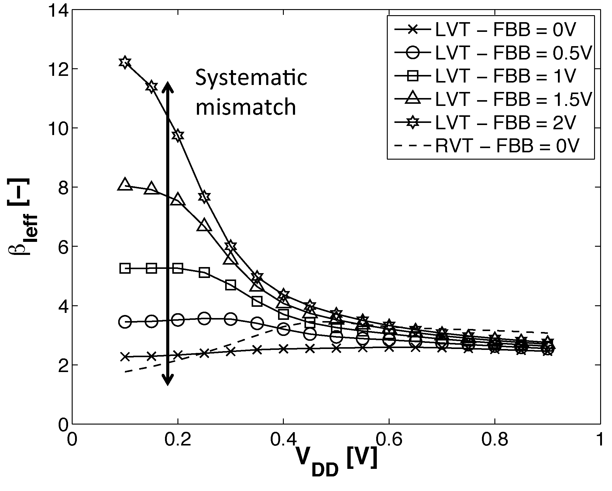
  • ADFBB: As shown in Figure 9, the PMOS I e f f boost with DFBBVDD compensation is not strong enough at low V D D , and β I e f f diverges from its value in the super-threshold domain, where standard cells are designed. In this scheme, the optimal adaptive DFBB (ADFBB) at each V D D is applied to the PMOS device to equalize rising and falling delays for an inverter;
  • IADFBB: The goal of this scheme is to achieve the same delay equalization as with ADFBB by reducing the NMOS I 0 with a negative BB instead of boosting the PMOS I 0 .
Figure 11 presents the rise-fall delay ratio β d e l = T f a l l / T r i s e for each scheme. We can see that the two adaptive schemes lead to a very stable rise-fall delay ratio over V D D . At high FBB, the DFBBVDD scheme cannot compensate for the I e f f drift between NMOS and PMOS. We then expect the most spectacular energy savings between (I)ADFBB and DFBBVDD to be seen for high speed devices.
For the ADFBB scheme, we can see that optimal DFBB is equal to V D D , plus a constant over every supply voltage. The same conclusion can be drawn for the IADFBB scheme keeping in mind that Figure 11 only features the DFBB applied to the NMOS, which is the constant part, and an FBB equal to V D D is simultaneously applied on the PMOS. This suggests that the systematic mismatch on I 0 , S and η between NMOS and PMOS is roughly constant over V D D .
Figure 10. Schematic view of LVT device in 28-nm UTBB FDSOI technology from STMicroelectronics with a description of the symmetric and asymmetric back biasing schemes.
Jlpea 04 00168 g010
Figure 11. The impact of ADFBB and IADFBB schemes as defined in Figure 10 on the inverter rise-fall delay ratio. From left to right: IADFBB optimal DFBB applied on NMOS, IADFBB rise-fall delay ratio, DFBB V D D (DFBBVDD) rise-fall delay ratio, ADFBB rise-fall delay ratio, ADFBB optimal DFBB applied on PMOS ( W p = 140 nm, W n = 80 nm, L p = L n = 30 nm).
Jlpea 04 00168 g011
The constant contribution of the optimal DFBB increasing with FBB and the β I e f f augmentation at high FBB suggest that systematic mismatch is stronger for lower threshold voltages.
The granularity in the optimal DFBB for V D D > 0.5 V can be explained by the limited sensitivity of the inverter delay with respect to V T . When the inverter is not in the subthreshold region, this low derivative causes the optimal DFBB extraction method to reach the precision limit of the simulation.

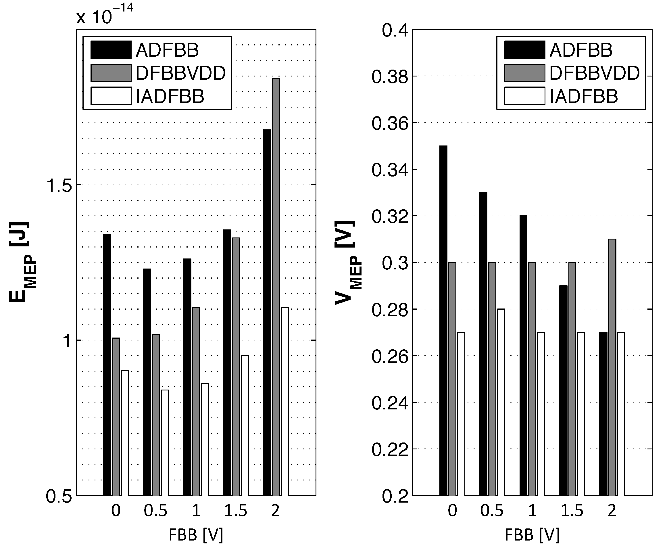
3.3. Impact of Back Biasing Compensation Schemes on the Minimum Energy Point

To study the evolution of the MEP with FBB and DFBB schemes, we implemented an eight-bit multiplier with RVT devices and LVT-FBB = 0 V devices as baselines. We then applied, on the LVT implementation, an increasing FBB from 0 V to 2 V with the three DFBB schemes described in Section 3. Multiplier delay was extracted by fitting a lognormal distribution over the Monte Carlo simulations and taking the mean value plus 3σ as a worst case value. Multiplier leakage power was estimated by the arithmetic mean over Monte Carlo simulations. All simulations were completed using the ELDO simulator from Mentor with 28-nm FDSOI CMOS models from STMicroelectronics, and only self loading was considered.
Figure 12 shows the E M E P and the V D D at which this energy is attained V M E P . For the (I)ADFBB schemes, the optimal DFBB at V D D = V M E P from Figure 11 was used. We can see that E M E P is increasing as the FBB voltage is increased. As V T is reduced, the MOSFETs enter the near-threshold regime, which results in higher E l e a k [18].
Figure 12. (Left) minimal E C y c l e for five FBB and for the three DFBB schemes; (right) V D D at the minimum energy point (MEP) for five FBB and for the three DFBB schemes.
Jlpea 04 00168 g012
Different results were obtained by [9] on the same simulation framework for 45-nm bulk technology. In bulk nodes, E M E P improvement for low- V T devices is linked to different phenomena compared to FDSOI. The V T reduction in bulk technologies is done by lowering channel doping, which narrows the channel depletion region, improves the subthreshold slope, reduces the gate leakage contribution, but increases the DIBL effect. Therefore, in the bulk process, an optimal V T exists, resulting from the tradeoff between DIBL mitigation, gate leakage reduction and subthreshold current improvement [9].
In the FDSOI process, V T variation is obtained by variating the back plane (BP) doping below the buried oxide [22], as shown in Figure 10, leaving the channel undoped, and V T variations will not modify the depletion of the channel. As shown by measures realized on an analog FDSOI process in [23], both S and η are increased with FBB. Increasing the V T on FDSOI technologies will not lead to an E M E P reduction.
Figure 13 shows the evolution of E M E P and f M E P with FBB. Having access to a continuous V T design space gives the possibility to shift MEP depending on the computational workload. Traditional subthreshold circuits try to approach MEP by scaling down V D D , but are forced to move away from it if a higher throughput is needed. Dynamically adaptive FBB could help keep the circuit near the MEP under a varying target frequency.
Figure 13. The MEP position in the target frequency design space for five FBB and for the three DFBB schemes.
Jlpea 04 00168 g013
For small FBB, using ADFBB leads to degraded E M E P levels, but at high FBB, which will allow higher f M E P , E M E P with ADFBB is below E M E P with DFBBVDD. This result is coherent with observations made from Figure 9 and Figure 11 that the DFBBVDD scheme is not adequate at high FBB. As ADFBB consists of boosting PMOS devices, the f M E P increases. On the opposite, IADFBB slows down NMOS devices to match the PMOS delay, leading to a reduced f M E P . As shown in Figure 12, IADFBB can offer an E M E P level reduction of 11 % at FBB = 0 and up to 18 % at FBB = 0.5 V.
To objectively compare the interest of ADFBB and IADFBB schemes, we represented in Figure 13 the position of the MEP as a function of the frequency at which this energy optimum is attained. Results indicate that IADFBB always leads to a lower E M E P value, but at the cost of a lower f M E P . IADFBB can reduce by 18 % the MEP level compare to DFBBVDD. On the contrary, ADFBB allows higher f M E P at the cost of E M E P degradation at low FBB, but with E M E P improvement at high FBB. Figure 13 also shows that FBB = 2 V with ADFBB can improve the MEP frequency by 36× compared to FBB = 0 V with DFBBVDD.
The Pwell/Nwell and Nwell/Psub diodes were not simulated. For a positive value of FBB and with the DFBB values shown in Figure 9, these diodes are reverse-biased. To ensure that their leakage current is negligible, we estimated the diodes’ area and perimeter for the eight-bit multiplier implemented with standard cells. In the worst case, for high a FBB value and for the three DFBB schemes, the total leakage power is below 30 fW at 25 C and below 70 pW at 125 C. This confirms that the leakage power of well diodes is negligible compared to the power of the multiplier.

3.4. Impact of Back Biasing Compensation Schemes on Robustness

Along with its impact on minimum energy, systematic mismatch between NMOS and PMOS currents leads to the reduced robustness of logic levels against crosstalk, radiations or random variability. In the subthreshold domain, where the I O N / I O F F ratio is small, these phenomena, including within die V T variability, can lead to insufficient noise margins ( N M L and N M H ) and to functional failure, as defined in [7]. At first order and without the DIBL effect, we can reduce Equation (2) and express ON-state and OFF-state currents as:
I O N = I 0 × 10 V D D S , I O F F = I 0
We consider I O N , N / I O F F , P and I O N , P / I O F F , N ratios as figures of the merit of robustness, which is a variation of the equivalent resistance model developed in [24]. We then discuss the theoretical impact of I 0 , S and η mismatch on these ratios:
I 0 :
As the two ratios depend linearly on I 0 , N / I 0 , P and I 0 , P / I 0 , N , having I 0 , N I 0 , P will favor one noise margin over the other and lead to a decreased global noise margin. Indeed, the gate noise margin is defined as m i n [ N M L , N M H ] ;
S:
If S N > S P , the I O N , N / I O F F , P ratio will be reduced, as it can be written as 10 ( - V T 0 + γ V B S ) / S N × 10 V D D / S N × 10 ( V T 0 - γ V B S ) / S P . A subthreshold swing mismatch will then lead to favoring one noise margin over the other;
η:
In the subthreshold domain, the DIBL effect increases both NMOS and PMOS currents in the same proportions. If the DIBL effect between the two devices is different, one drive current will be increased, but when the high DIBL device does not drive, the high leakage and low drive device will lead to reduced robustness.
In each case, maximizing the I O N , N / I O F F , P and I O N , P / I O F F , N ratios is done with balanced devices.
In order to evaluate the impact of ADFBB and IADFBB on yield, we estimate the noise margins as proposed in [7] based on 80 k Monte Carlo simulations of a NAND2 gate cross-coupled with a NOR2 gate. As the NOR2 gate features a stacked pull-up network, it has the most stringent constraint on low input noise margin V I L , and similarly, the NAND2 gate has the most stringent noise margin constraint on its low output level V O L . Without precise information about the circuit paths, the considered benchmark can give an interesting figure of merit of the functional failure probability at the gate level.
To obtain an image of functional die yield based on this gate SNM extraction technique, we used a framework developed in [6] where the authors extrapolate die yield η d i e as follows:
η d i e = η g a t e N g a t e s / 2
where η g a t e is the gate yield computed with the Monte Carlo simulations.
To consider the impact of noise and crosstalk, gate functional failure was defined as NOR2-NAND2 SNM below two thresholds: 30 mV and 40 mV. Using this model, we can compare the die yield depending on the gate count using or not using the (I)ADFBB compensation as plotted in Figure 14.
Results indicate that having a 95 % die yield with RVT devices limits the gate count to 80 k gates for 40 mV minimum SNM, while using LVT devices can bring this limit to 320 k gates. As predicted, balancing the I 0 between NMOS and PMOS has a positive impact on die yield. Figure 14 shows that, at a 30-mV minimum SNM, we can improve by a factor of six the number of gate at a 95 % die yield. At 40-mV minimum SNM, the improvement factor between LVT and LVT with (I)ADFBB is higher than 4×.
The inset in Figure 14 indicates that a similar maximum number of gates at a 95 % die yield can be achieved with IADFBB and with ADFBB, which is coherent with the idea that these two techniques are two equivalent ways to balance I e f f , N and I e f f , P . The inset in Figure 14 also shows the optimal value of DFBB to be applied to maximize robustness. The two maxima appears at different DFBB values, because they are applied differently in IADFBB and in ADFBB, as shown on Figure 10. We can also see that the optimum DFBB values in each case for robustness is close to the optimum DFBB values found in Section 3.3 for energy minimization.
Figure 14. Functional yield computed with the model described by Equation (14) for an eight-bit multiplier @ V D D = 0.3 V implemented with RVT and LVT devices (FBB = 0 V). The gate noise margins were considered with two thresholds: 30 mV and 40 mV. Inset: the maximum number of gates to maintain a 95 % die yield with the ADFBB and IADFBB schemes.
Jlpea 04 00168 g014

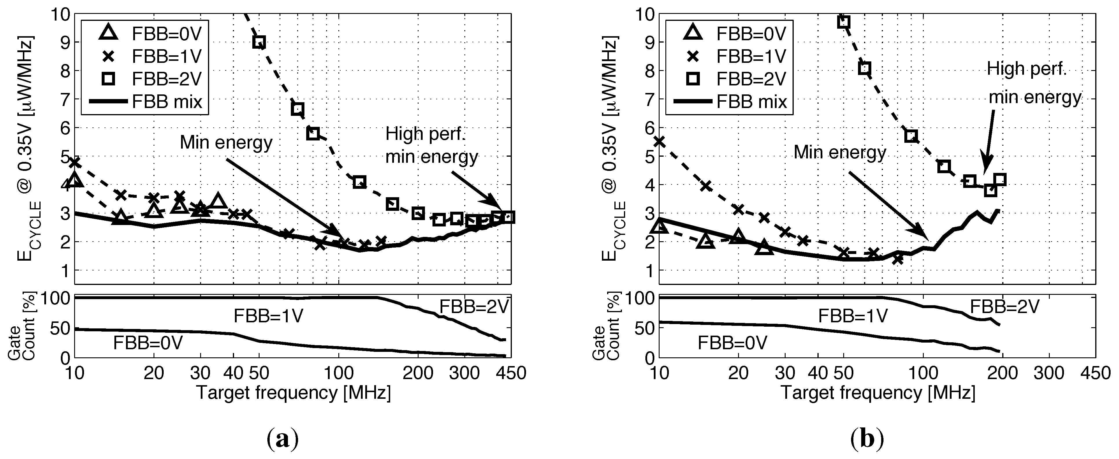
4. Back Biasing Analysis at the Standard Cell Library Level

For 28-nm FDSOI, we recharacterized the LVT standard-cell libraries from STMicroelectronics at 0.35 V using the Liberate tool from Cadence and the ELDO simulator from Mentor. Three versions of the library were computed at FBB = 0, 1 and 2 V. In order to characterize the impact of FBB on the lib, we examine the 20 most used cells in the two microcontroller cores synthesized and presented in Section 5. Figure 15a shows a mean rise-fall transition time drop of 20 % to 40 % from FBB = 0 V to FBB = 1 V and a 30 % to 50 % delay reduction between FBB = 0 V and FBB = 2 V, depending on the cells.
Figure 15c shows that the mean leakage between FBB = 0 V and FBB = 1 V is around 10× and as high as 100× between FBB = 0 V and FBB = 2 V, due to the I O F F exponential dependance on V T .
Figure 15. Timing, switching power and leakage power factors of merit for the three recharacterized libraries for the 20 most used cells in the synthesized microcontroller core from Section 5. (a) Mean of rise-fall timing entries for 20 cells of the recharacterized libraries; (b) mean of rise-fall power entries for 20 cells of the recharacterized libraries; (c) mean of the leakage entries for 20 cells of the recharacterized libraries.
Jlpea 04 00168 g015

5. Back Biasing Analysis at the IP Level

To asses these FoMs at the block level for ULV SoCs with high computing capabilities, let us consider two benchmark circuits: a 16-bit MSP430-compatible core from [25] as modified at UCL in the SleepWalker SoC [4] (including its instruction cache memory I $ and some peripherals) and the commercially-available ARM Cortex-M0 DesignStart 32-bit core. We ran a synthesis of these two cores, both in 65-nm bulk CMOS and in 28-nm FDSOI at 0.35 V with the recharacterized libraries presented in Section 4. For 65 nm, standard-cell libraries with UGL from [4] were considered. Synthesis was considered for each of these versions separately and with a mix of the three versions.
Figure 16a,b shows that synthesis with high FBB can achieve the timing closure at high frequencies. The M0 can be clocked at 440 MHz in 28-nm FDSOI with FBB = 2 V achieving a speed up of 8.8× compared to 65 nm. However, as the core leaves the subthreshold region ( V T becomes lower than V D D , resulting in a higher leakage energy), the E C Y C L E is higher compared to the energy achieved at a lower FBB. At a low frequency, high FBB implementations suffer from energy overhead, due to the integration of the high leakage power over a long cycle time. By allowing the synthesis tool to use a mix between the 3FBB library versions, we manage to keep the energy per cycle below 3 μW/MHz through almost all of the frequency design space. The evolution of the gate count breakdown between the three FBB library versions with frequency shows that faster gates are introduced in the design when the timing closure cannot be met with the previous FBB. Two key results are identified: the strict minimum energy point that is reached in the frequency range using mainly gates with 0- and 1-V FBB and the high-speed minimum energy point using also 2-V FBB gates. Figure 17a illustrates the speed-up and energy savings between 65-nm bulk and 28-nm FDSOI implementations. We achieve on the M0 a 42 % E C Y C L E reduction and a 7× speed up if we target high performance or a 64 % E C Y C L E reduction and a 2.4× speed up if we target energy minimization, compared to the 65-nm baseline. The difference between the E C Y C L E reductions of the two cores comes from the different contributions of leakage and switching energy to E C Y C L E .
Figure 16. Energy per cycle vs. the synthesis frequency for the Cortex M0 and for the swMSP430 with each FBB library version and with the mix of all three versions. (a) ARM Cortex M0; (b) swMSP430.
Jlpea 04 00168 g016
Figure 17. Energy per cycle of synthesized cores depending on the frequency or depending on the FBB at synthesis. (a) Evolution of the two energy minima at 0.35 V for swMSP430 and Cortex M0 between the 65-nm baseline and the 28-nm FDSOI optimized implementation; (b) energy per cycle for the Cortex M0 synthesized using FBB = 0 V, 1 V or 2 V at 30 MHz and running at different speeds, depending on the applied FBB.
Jlpea 04 00168 g017
In practical applications, it would be interesting to know how the FBB used during the synthesis influences the energy efficiency in the operation. For a given target frequency, the designer has the choice of synthesizing the IP with a low or high FBB library. A slow synthesized core can then be speeded up by applying a higher FBB during operation. Conversely, the core synthesized with a high speed library can be slowed down with lower FBB in operation. Figure 17b shows the energy per cycle for the ARM Cortex M0 synthesized and operated with the three FBB libraries. The core synthesized at FBB = 0 V is energy inefficient for high FBB, high speed operations, and the core synthesized at FBB = 2 V maintain good energy efficiency over the entire range of FBB. In conclusion, in order to take advantage of the electrical control over the frequency of operation offered by the forward back biasing and still maintain good energy efficiency, the synthesis operation should be conducted with a library characterized at high FBB.

6. Conclusions

The development of ultra-low-power embedded devices, such as wireless sensor nodes, calls for the Internet-of-Things for both very low energy per operation and high optimal frequency. Increasing the impact of short channel effects and variability on advanced bulk nodes degrades the minimum energy level at ULV in the sub-90-nm CMOS node. At the gate level, we showed that 28-nm UTBB FDSOI with a smaller impact of the short channel effects and a reduced variability can provide the MEP level reduction by a factor 5.5 compared to the 45-nm bulk node. We proposed to use the FBB to shift the MEP toward higher operating frequencies with a limited energy penalty. Dynamic FBB modifications can thus be used to dynamically adapt the clock frequency to the fluctuating computational workload. We also provide a new method for systematic mismatch cancellation between NMOS and PMOS subthreshold currents for different FBB voltages. Adaptive and inverse adaptive FBB further extend the range of frequencies, which leads to an energy minimum. Such adaptive schemes that are used to modify the speed/energy trade-off can reduce the MEP value by 18 % , increasing the speed 36×.
With the development of complex subthreshold circuits, keeping a reasonable functional yield will became more challenging. The ADFBB and IADFBB schemes can provide a gate count improvement for a 95 % yield up to a factor of 6×.
At the IP level, we showed that UTBB FDSOI can provide either leakage reduction at low-speed or high-speed operations, while maintaining E C Y C L E below the E C Y C L E achieved in 65 nm and improving robustness in ULV. Compared to 65-nm bulk, synthesis results show that the speed of ULV microcontrollers in 28-nm FDSOI can be boosted by a factor of 7× in 28-nm FDSOI, and the E C Y C L E can be reduced by 64 % with a mix of overdrive FBB voltages. We also showed that mixing FBB during synthesis can lead to an energy-efficient implementation for a wide range of frequencies of operation and that a microcontroller core synthesized at high speed can be kept energy efficient, even at low speed, when a lower FBB is applied in operation.
An interesting research direction for future work would be to first investigate the practical implementation of the FBB and DFBB schemes at the layout level to minimize the die area and energy consumption overhead for FBB generation, routing and optimum tracking.

Acknowledgments

Guerric de Streel is with the Université catholique de Louvain as a research fellow from the National Foundation for Scientific Research (FNRS) of Belgium through a Fonds pour la formation Ãă la Recherche dans l’Industrie et dans l’Agriculture (FRIA) grant.

Conflicts of Interest

The authors declare no conflict of interest.

References

  1. Bol, D.; de Vos, J.; Botman, F.; de Streel, G.; Bernard, S.; Flandre, D.; Legat, J.-D. Green SoCs for a Sustainable Internet-of-Things. In Proceedings of the IEEE Faible Tension Faible Consommation (FTFC), Paris, France, 20–21 June 2013.
  2. Wang, A.; Chandrakasan, A.P.; Kosonocky, S.V. Optimal Supply and Threshold Scaling for Subthreshold CMOS Circuits. In Proceedings of the IEEE Computer Society Annual Symposium on VLSI Proceedings, Pittsburgh, PA, USA, 25–26 April 2002; pp. 5–9.
  3. Calhoun, B.H.; Wang, A.; Chandrakasan, A. Device Sizing for Minimum Energy Operation for Subthreshold Circuits. In Proceedings of the IEEE Custom Integrated Circuits Conference, City, Country, 3–6 October 2004; pp. 90–95.
  4. Bol, D.; de Vos, J.; Hocquet, C.; Botman, F.; Durvaux, F.; Boyd, S.; Flandre, D.; Legat, J. SleepWalker: A 25-MHz 0.4-V Sub-mm2 7-μW/MHz microcontroller in 65-nm LP/GP CMOS for low-carbon wireless sensor nodes. IEEE J. Solid-State Circuits 2013, 48, 20–32. [Google Scholar] [CrossRef]
  5. Abouzeid, F.; Clerc, S.; Pelloux-Prayer, B.; Argoud, F.; Roche, P. 28 nm CMOS, Energy Efficient and Variability Tolerant, 350 mV-to-1.0V, 10 MHz/700 MHz, 252 Bits Frame Error-Decoder. In Proceedings of the ESSCIRC, Bordeaux, France, 17–21 September 2012; pp. 153–156.
  6. Bol, D. Robust and energy-efficient ultra-low-voltage circuit design under timing constraints in 65/45 nm CMOS. J. Low-Power Electron. Appl. 2011, 1, 1–19. [Google Scholar] [CrossRef]
  7. Kwong, J.; Chandrakasan, A. Variation-Driven Device Sizing for Minimum Energy Sub-Threshold Circuits. In Proceedings of the International Symposium on Low Power Electronics and Design (ISLPED’06), Tegernsee, Germany, 4–6 October 2006; pp. 8–13.
  8. Alioto, M. Ultra-low power VLSI circuit design demystified and explained: A tutorial. IEEE Trans. Circuits Syst. I 2012, 59, 3–29. [Google Scholar] [CrossRef]
  9. Bol, D.; Flandre, D.; Legat, J.-D. Technology Flavor Selection and Adaptive Techniques for Timing-Constrained 45 nm Subthreshold Circuits. In Proceedings of the 14th ACM/IEEE International Symposium on Low Power Electronics and Design (ISLPED ’09), San Fancisco, CA, USA, 19–21 August 2009; pp. 21–26.
  10. Flatresse, P. Product Vision on Planar Fully Depleted Technology FD28 nm for Mobile Applications. In Proceedings of the IEEE International SOI Conference, Napa, CA, USA, 1–4 October 2012.
  11. Bol, D.; Flandre, D.; Legat, J.-D. Nanometer MOSFET effects on the minimum-energy point of sub-45 nm subthreshold logic—Mitigation at technology and circuit levels. ACM Trans. Des. Autom. Electron. Syst. 2010, 16, 1–26. [Google Scholar] [CrossRef]
  12. Bol, D.; Ambroise, R.; Flandre, D.; Legat, J.-D. Sub-45 nm Fully-Depleted SOI CMOS Subthreshold Logic for Ultra-Low-Power Applications. In Proceedings of the IEEE International SOI Conference (SOI), New Paltz, NY, USA, 6–9 October 2008.
  13. Bol, D.; Bernard, S.; Flandre, D. Pre-Silicon 22/20 nm Compact MOSFET Models for Bulk vs. FD SOI Low-Power Circuit Benchmarks. In Proceedings of the IEEE International SOI Conference (SOIC), Tempe, AZ, USA, 3–6 October 2011.
  14. Pu, Y.; de Gyvez, J.P.; Corporaal, H.; Ha, Y. Vt Balancing and Device Sizing toward High Yield of Sub-Threshold Static Logic Gates. In Proceedings of the 2007 International Symposium on Low Power Electronics and Design (ISLPED), Portland, OR, USA, 27–29 August 2007; pp. 355–358.
  15. Hwang, M.E.; Roy, K. ABRM: Adaptive β-ratio modulation for process-tolerant ultradynamic voltage scaling. IEEE Trans. VLSI Syst. 2010, 18, 281–290. [Google Scholar] [CrossRef]
  16. De Streel, G.; Bol, D. Impact of Back Gate Biasing Schemes on Energy and Robustness of ULV Logic in 28 nm UTBB FDSOI Technology. In Proceedings of the IEEE International Symposium on Low Power Electronics and Design (ISLPED), Beijing, China, 4–6 September 2013; pp. 255–260.
  17. De Streel, G.; Bol, D. Scaling Perspectives of ULV Microcontroller Cores to 28 nm UTBB FDSOI CMOS. In Proceedings of the IEEE SOI-3D-Subthreshold Microelectronics Technology Unified Conference (S3S), Monterey, CA, USA, 7–10 October 2013; pp. 1–2.
  18. Calhoun, B.H.; Wang, A.; Chandrakasan, A. Modeling and sizing for minimum energy operation in subthreshold circuits. IEEE J. Solid-State Circuits 2005, 40, 1778–1786. [Google Scholar] [CrossRef]
  19. Bol, D.; Ambroise, R.; Flandre, D.; Legat, J. Interests and limitations of technology scaling for subthreshold logic. IEEE Trans. VLSI Syst. 2009, 17, 1508–1519. [Google Scholar] [CrossRef]
  20. Na, M.H.; Nowak, E.J.; Haensch, W.; Cai, J. The Effective Drive Current in CMOS Inverters. In Proceedings of the International Electron Devices Meeting (IEDM), San Francisco, CA, USA, 8–11 December 2002; pp. 121–124.
  21. Ono, G.; Miyazaki, M. Threshold-voltage balance for minimum supply operation. IEEE J. Solid-State Circuits 2003, 38, 830–833. [Google Scholar] [CrossRef]
  22. Thomas, O.; Noel, J.-P.; Fenouillet-Beranger, C.; Jaud, M.-A.; Dura, J.; Perreau, P.; Boeuf, F.; Andrieu, F.; Delprat, D.; Boedt, F.; et al. 32 nm and beyond Multi-VT Ultra-Thin Body and BOX FDSOI: From Device to Circuit. In Proceedings of the IEEE International Symposium on Circuits and Systems (ISCAS), Paris, France, 30 May–2 June 2010; pp. 1703–1706.
  23. Kilchytska, V.; Flandre, D.; Andrieu, F. On the UTBB SOI MOSFET Performance Improvement in Quasi-Double-Gate Regime. In Proceedings of the European Solid-State Device Research Conference (ESSDERC), Bordeaux, France, 17–21 September 2012; pp. 246–249.
  24. Pu, Y.; de Gyvez, J.P.; Corporaal, H.; Yajun, H. Statistical Noise Margin Estimation for Sub-Threshold Combinational Circuits. In Proceedings of the Asia and South Pacific Design Automation Conference (ASPDAC), Seoul, Korea, 21–24 March 2008; pp. 176–179.
  25. Girard, O. OpenMSP430 Project, 2010: Opencore.org.
  26. Weber, O.; Faynot, O.; Andrieu, F.; Buj-Dufournet, C.; Allain, F.; Scheiblin, P.; Foucher, J.; Daval, N.; Lafond, D.; Tosti, L.; et al. High Immunity to Threshold Voltage Variability in Undoped Ultra-Thin FDSOI MOSFETs and Its Physical Understanding. In Proceedings of the IEEE International Electron Devices Meeting (IEDM), San Francisco, CA, USA, 15–17 December 2008; pp. 1–4.

