Review

An Ultra-Low Energy Subthreshold SRAM Bitcell for Energy Constrained Biomedical Applications †

The Charles L. Brown Department of Electrical and Computer Engineering, University of Virginia, Charlottesville, VA 22904, USA
*
Author to whom correspondence should be addressed.
The original of this paper had been presented in IEEE S3S Conference 2013.
J. Low Power Electron. Appl. 2014, 4(2), 119-137; https://doi.org/10.3390/jlpea4020119
Submission received: 1 March 2014 / Revised: 6 May 2014 / Accepted: 19 May 2014 / Published: 27 May 2014
(This article belongs to the Special Issue Selected Papers from IEEE S3S Conference 2013)

Abstract

:
Energy consumption is a key issue in portable biomedical devices that require uninterrupted biomedical data processing. As the battery life is critical for the user, these devices impose stringent energy constraints on SRAMs and other system on chip (SoC) components. Prior work shows that operating CMOS circuits at subthreshold supply voltages minimizes energy per operation. However, at subthreshold voltages, SRAM bitcells are sensitive to device variations, and conventional 6T SRAM bitcell is highly vulnerable to readability related errors in subthreshold operation due to lower read static noise margin (RSNM) and half-select issue problems. There are many robust subthreshold bitcells proposed in the literature that have some improvements in RSNM, write static noise margin (WSNM), leakage current, dynamic energy, and other metrics. In this paper, we compare our proposed bitcell with the state of the art subthreshold bitcells across various SRAM design knobs and show their trade-offs in a column mux scenario from the energy and delay metrics and the energy per operation metric standpoint. Our 9T half-select-free subthreshold bitcell has 2.05× lower mean read energy, 1.12× lower mean write energy, and 1.28× lower mean leakage current than conventional 8T bitcells at the TT_0.4V_27C corner. Our bitcell also supports the bitline interleaving technique that can cope with soft errors.

Graphical Abstract

1. Introduction

Portable biomedical devices requiring long-term data processing have stringent energy requirements. This includes portable electrocardiograms (ECG), electromyograms (EMG), and electroencephalograms (EEG) type devices that can process critical disease related data at operating frequency ranging from a few hundred kHz to a few MHz [1,2]. These devices impose energy constraints on biomedical system on chip (SoC) components and SRAM design. Due to the square law dependency of energy with supply voltage, scaling down the supply voltage reduces energy in logic and SRAMs in SoCs. In a CMOS process, reducing the supply voltage below the threshold voltage (VT) of the MOSFET makes it enter into the subthreshold region. Prior works have shown that operating both logic and memory in subthreshold supply voltages reduces energy dissipation and minimizes energy per operation [3,4]. Although voltage-scaling increases delay in logic and SRAMs, subthreshold logic and SRAMs provide enough performance to meet the throughput requirements for the biomedical devices.
On the other hand, due to device variations in subthreshold SRAMs, the conventional 6T bitcell has poor read static noise margin (RSNM) [5] and is unreliable for subthreshold operation. There are many proposed subthreshold bitcells [6,7,8,9] present in the literature having some improvement in write-ability and read stability related design metrics by trading-off other metrics. However, subthreshold bitcells such as the 8T [10] bitcell, face half-select [8] problems in a (column) mux scenario, which can cause read-disturb and unnecessary energy drainage during a write operation. This imposes further constraints on usage of write assists such as the boosted wordline [11,12] due to degraded read stability in half-selected [12] bitcell.
In order to avoid this half-select problem, we either can implement read-before-write operation [7,13] instead of normal write in SRAMs or we can design half-select-free SRAM bitcells [7,8,9,14] that decouple read and write operations. However, implementing read-before-write SRAM architectures in subthreshold supply voltages can be a more complex and time-consuming task than designing a simple column mux based SRAM design. On the other hand, in subthreshold memories, soft error disturbs (SED) are critical [15], and bitline interleaving in memory architecture [7] uses column multiplexing to improve on SED.
Given all these subthreshold bitcells, their design trade-offs and various architecture related issues, we compare our subthreshold bitcell with available subthreshold bitcells in a column mux scenario. In this work, we assume that applying appropriate peripheral read and write assist methods [11,12] can solve read stability [12] and write-ability [11] related known issues in subthreshold SRAM bitcells with less penalty in energy per operation and area standpoint in an SoC. In addition, we also assume that we can trade-off SRAM area for better energy efficiency, since it is of less importance in biomedical applications. In this simulation-based paper, we compare our bitcell to the state of the art subthreshold SRAM bitcells from various SRAM design knob perspectives across a set of design metrics for biomedical applications. The rest of this paper is divided into seven sections. In Section 2, we introduce the state of the art subthreshold SRAM bitcell topologies. Section 3 talks about the limitations of the available subthreshold bitcells including the half-select issue. In Section 4, we introduce our half-select-free 9T subthreshold SRAM bitcell. Section 5 describes the concept of minimum energy per operation and read-write weighted energy per operation. In Section 6, we describe the experimental setup for comparison of the subthreshold SRAM bitcells. Section 7 presents the comparison results for various SRAM design knobs, and we conclude in Section 8.

2. Subthreshold Bitcells Topologies

The conventional 6T SRAM bitcell shown in Figure 1a is the most used bitcell topology in SRAMs. It has two back-to-back inverters, which act as a latch for storing logic “1” in one side, and “0” in the other side. There are two access transistors in the bitcell for both reading and writing. However, due to the poor read static noise margin [5] (RSNM) and half-select [12] issue, the 6T bitcell is not robust in subthreshold supply voltages. Almost all other SRAM bitcells, including subthreshold bitcells, are modified versions of the 6T. The most common subthreshold SRAM bitcell derived from the 6T is the conventional 8T subthreshold bitcell [10] with a 2T read buffer as shown in Figure 1b. The 2T read buffer senses the information stored in the bitcell in read operation. The conventional 8T allows decoupled read and write operations, which enable us to size the read and write path differently. This adds another knob for energy efficient design exploration with the 8T bitcell. Another subthreshold bitcell with reportedly lower minimum operating voltage (VMIN) is the Schmitt-trigger based bitcell [6] (Figure 1c). This bitcell uses the hysteresis property of a Schmitt-trigger to strengthen the read operation still allowing lower VMIN. Although the conventional subthreshold 8T and Schmitt-trigger based bitcells are robust in read and write operations, they are costly from an energy standpoint if used in a column mux scenario. This is due to the inherent half-select problem [12] in the 8T and Schmitt-trigger based bitcells in a write operation. There are many half-select-free bitcells available in the literature like Chang’s 10T [7] (Figure 1d), Feki’s 10T [8] (Figure 2a), and Chiu’s 8T [9] shown in Figure 2b. Although Yang’s 8T [14] (Figure 2c) is not mentioned as a subthreshold bitcell, due to structural symmetry with Chiu’s bitcell, we include this bitcell for comparison in this paper. In most of the cases, these half-select-free bitcells have two separate wordlines for read and write. This allows us to size the read and write path independently such as Feki’s bitcell. On the other hand, Chang’s, Yang’s and Chiu’s bitcell has common read or write nodes, which prevents sizing their read and write paths independently. All of this work has shown some improvements in read stability, write-ability, VMIN, and leakage metrics. In this paper, we show how our bitcell compare with state of the art subthreshold SRAM bitcells from the energy and delay metrics and the energy per operation metric perspective across various SRAM design knobs. As subthreshold designs are better suited to be designed with a lower leakage technology, we prefer an older technology for subthreshold design. We compare the bitcell using a commercial 130 nm technology in a typical typical corner (TT) as the 130 nm technology is very stable nowadays and it is available to us. As the applications targeted in this work are biomedical applications for Body Area Sensor Node (BASN) [1] applications, we use room temperature conditions of 27 °C for the comparion simulations in this paper.
Figure 1. (a) 6T SRAM bitcell; (b) Conventional 8T SRAM subthreshold bitcell; (c) Kulkarni’s schmitt-trigger based subthreshold SRAM bitcell; (d) Chang’s 10T subthreshold bitcell.
Jlpea 04 00119 g001
Figure 2. (a) Feki’s 10T SRAM subthreshold bitcell; (b) Chiu’s 8T subthreshold bitcell; (c) Yang’s 8T SRAM bitcell.
Jlpea 04 00119 g002

3. Limitations of Available Bitcells

Bitcells discussed in the previous section are not free from drawbacks. Although, Kulkarni’s bitcell has the lowest reported VMIN, it can consume more dynamic and leakage energy due to its Schmitt-trigger based feedback structure. The Schmitt-trigger based feedback structure uses the additional transistors M9 and M10 (Figure 2c) to strengthen the internal storage node resulting in higher dynamic energy dissipation and creates a greater number of source or sink paths causing more leakage current. Secondly, Kulkarni, Feki and Chang’s bitcells have a 10T structure that inherently should burn more dynamic energy as those bitcells have more transistors than the 8T, Chiu and Yang’s bitcells. This is due to the assumption that we size all the bitcells with respect to a set of common reference design metrics and thus extra transistors in bitcells will add to the increase of dynamic energy. Moreover, we can see that Chang’s bitcell adds more leakage paths by introducing transistors M7 and M8 creating two additional leakage paths from bitline to ground, such as paths BLB-M9-M7-VSS, BL-M10-M8-VSS. In addition, assuming that the bitcell back-to-back inverter sizes are the same and each of the control signals such as wordlines have the same activity factor, bitcells having multiple wordlines as control signals—such as Chang’s, Feki’s, and Yang’s bitcells—should drain more dynamic energy than bitcells having fewer wordline control signals triggered per read or write operation. Thirdly, bitcells those use the same path for read and write operations—such as Kulkarni’s, Chiu’s, and Chang’s bitcells—should experience energy consumption due to precharging bitlines after the end of both read and write cycles. Moreover, in the column mux scenario, unselected bitcells in the same row are half-selected and they experience read stress in the write operation. Not only Kulkarni’s bitcell, but also conventional subthreshold 8T bitcells such as Chiu and Yang’s suffer from the half-select problem in the write operation. Hence, in order to capture all the aforementioned potential sources of energy dissipation, we need to simulate all these bitcells in a column mux scenario where all of these effects are taken into consideration.

3.1. SRAM Half-Select-Issue in Write Operation

Figure 3 shows the half-select problem in the presence of a column mux (CM) 4 in SRAM write operation. Here, our assumption is that the SRAM has multiple banks. Each of the SRAM banks has the same sized core array comprised of subthreshold bitcells. It shows that in column mux 4 scenarios, every four-bitcell columns constitute a single I/O column, which has precharge logic, read and write column muxes, write driver, and read logic. When a user asserts an SRAM address, it selects a word in an SRAM row by selecting one of the bank’s physical rows and multiple physical columns. For example, if the user selects the first word in the row, then it selects only the first physical bitcell column of every four physical bitcell columns. Other bitcells in the same row being row wise selected but column wise unselected are half-selected bitcells. In write operation, these half-selected bitcells undergo read stress as if they are in a read operation, and it causes unnecessary energy drainage. Another potential issue with the half-select problem is that using wordline boost type write-assist [11,12] for write-ability improvement can cause the half-selected bitcells to have destructive read. In other words, applying a wordline-boost type write assist can cause the half-selected bitcells to flip. However, it is easy to implement column mux based SRAM architectures as the complexity of this type of designs are much less compared to read-before-write [7,13] subthreshold SRAM architectures. Another way of avoiding the half-select issue is to use a half-select-free [9] subthreshold SRAM bitcell. With this type of bitcells, column mux based designs are easy to implement. However, proposed half-select-free bitcells have more devices and control signals, which can cause unnecessary dynamic and leakage energy drainage. Moreover, half-select-free subthreshold bitcells have shared nodes in read and write paths which can cause sizing issues.
Figure 3. Half-select problem in SRAM bitcells in column mux (CM) 4 scenario.
Jlpea 04 00119 g003

4. Proposed 9T Bitcell

The proposed bitcell [16] is shown in Figure 4a (WM1, M3 = 0.4u, LM1, M3, M5, M6, M7 = 0.22u, WM2, M4 = 0.28u, LM2, M4, M8, M9 = 0.15u, WM5, M6, M7 = 0.45u, and WM8, M9 = 0.36u). We choose the bitcell’s back-to-back inverter (M1, M2, M3 and M4) and two transistor read-buffer transistor (M8, M9) sizes as per a reference conventional subthreshold 8T bitcell size used in subthreshold SRAMs in a Body Area Sensor Node Chip (BASN) chip [1] at University of Virginia. We run Monte Carlo simulations for write margin, HSNM, read time, etc. design metrics to choose the transistor gate widths and lengths as non-minimum to cope with the subthreshold process variations. The bitcell consists of a set of back-to-back inverters like 6T, and a differential amplifier-like structure used for write access. For reading, we use a two transistor read buffer like the 8T read buffer [10]. During the write operation, only one of the write bitlines WBL or WBLB goes high (Figure 4a), while the other remains low. Meanwhile, the write-wordline WWL becomes high, and if the corresponding internal node was storing “1”, it is discharged through the write path. In write operation, pulling down WBL and WBLB nets of half-selected bitcells in the same SRAM row prevents the half-select issue. As our bitcell does not require any precharge operation of the write bitlines, it consumes less dynamic energy. In case of a read operation, we precharge the read bitline RBL to VDD, and trigger the read wordline RWL to evaluate the read (Figure 4a). Here, node Qb is the reference node in the read operation. If the content of the bitcell is such that Qb holds logic “1”, the RBL discharges, and this denotes a read “1” operation. Otherwise, if Qb holds logic “0”, RBL stays at VDD, which denotes a read “0” operation. In order to reduce standby leakage, the signals FTRR and FTRW only go to VDD while in standby mode, and they do not toggle in normal read or write operations. Hence, the default states of FTRR and FTRW are logic “0” s. In this 130 nm technology, we report the leakage improvement by pulling the FTRR and FTRW to VDD compared to leaving it at VSS is 34% at TT_0.4V_27C corner. This technique of pulling the footer to VDD can save significant leakage energy in lower technologies [10] too. Figure 4b shows the waveforms for read and write operations.
Figure 4. (a) Schematic of the proposed 9T bitcell; (b) Read (Rd)/Write (Wr) waveforms of proposed 9T bitcell.
Jlpea 04 00119 g004

5. Minimum Energy per Operation of Subthreshold SRAMs

In subthreshold supply voltages, delay increases exponentially with decreasing supply voltage. Due to this fact, in subthreshold SRAMs, the leakage energy per operation also increases exponentially with decreasing supply voltage. On the other hand, the SRAM dynamic energy per operation decreases with supply voltage scaling in SRAMs as shown in Figure 5. As a resulting effect, the total energy of the SRAM has a minimum energy point (Figure 5) which lies within the subthreshold supply voltage region. In fairly bigger subthreshold SRAMs, the core array contributes to most of the leakage energy per operation. As the SRAM core array bitlines have higher capacitance due to the presence of multiple bitcells in a column, a significant amount of dynamic energy can come from the array itself. In order to lower the SRAM minimum energy supply voltage point, we can either increase the dynamic energy per operation of the SRAM keeping the leakage energy per operation fixed. Otherwise, we can lower the leakage energy per operation keeping the dynamic energy fixed. In the first case, the minimum energy point (MEP) will shift corresponding to a lower supply voltage, but the energy per operation will increase. However, if we lower leakage energy per operation, we can get two-fold benefit of lowering MEP as well as lowering MEP supply voltage. On the other hand, if we lower the leakage and dynamic energy per operation at the same rate, the MEP supply voltage can remain the same; however, it reduces the MEP itself.
Figure 5. Minimum energy point of SRAMs.
Jlpea 04 00119 g005

5.1. Read-Write Weighted Energy per Operation and Fraction of Read and Write

In SRAMs, usually we do more read operations than write. In order to get an equivalent minimum energy point (MEP), we have to weigh the read and write energy per operations accordingly to get the read-write weighted energy per operation. We express this weighted average energy per operation as Equation (1).
Eavgop = Ewr × (1 − Frdwr) + Erd × Frdwr
Here, the parameter Eavgop denotes read-write weighted energy per operation; Ewr and Erd are the write and read energy per operation, respectively. In Equation (1), the parameter Frdwr is the fraction of read and write that denotes how many read operations on average are there out of total number of read-write operations. It is noticeable that if the Erd is lower than the Ewr, increasing the Frdwr parameter decreases the weighted energy per operation.

6. Experimental Setup

We do all our experiments in a commercial 130 nm technology at the TT_27C corner using Cadence’s Spectre simulator. For the mismatch analysis, we run 1000 Monte Carlo simulations for each comparison at VDD = 0.4 V. We perform two sets of experiments: one based on the experimental setup shown in Figure 6, where except from the actual drivers, we use voltage sources as input waveforms for comparisons of the energy and delay numbers. On the other hand, for comparison of the energy per operation metric, and to get the minimum energy point (MEP) data, we use the experimental setup shown in Figure 6a,b. Here, “WL” stands for wordline, “PREB” stands for precharge bar, and “WRITE_EN” stands for write enable. We use extracted inverter netlist from a standard cell library for the use of drivers for wordline, bitline and write enable, etc. signals. This will ensure that the rise and fall time of the buffer and inverter outputs to the wordlines, precharge enable, write enable, etc. signals are realistic in the subthreshold supply voltages. In each case of write and read setup shown in Figure 6a,b, we have two columns: the leftmost column represents the actual column for write or read setup, which has total modeled bitline load shown as rows per bank (RPB) times a single bitcell bitline load. On the other hand, the second column models the wordline load, which is column mux factor (CM) times a single bitcell wordline load. Overall, the setup models “RPB × CM” number of bitcells per set of physical bitcell-columns associated with a single column mux of an SRAM bank for dynamic energy measurement. For example, in an SRAM bank with CM = 4, we would have a set of four physical bitcell columns associated with each column mux 4 and with RPB = 16. In this case, our setup models the dynamic energy consumption of the set of four bitcell columns for 16 × 4 = 64 bitcells per column mux 4. For generating different energy, delay and MEP values, we simulate multiple instances with RPB = 4, 8, 16, 32 and 64 values. In order to generate dynamic energy values for different word-widths, we multiply set of columns’ (consisting of multiple bitline columns as per column mux) dynamic energy values across SRAM word-widths of 2, 4, 8, 16, and 32. For extracting the leakage numbers, we use single bitcells’ netlist with single voltage source for each circuit. We use these bitcell leakage values to generate the corresponding leakage values of the full SRAM core arrays. Finally, we added the modeled dynamic and leakage energy values for each SRAM macro to get the total energy values for minimum energy point calculations. We limit the observation of memory sizes from 2 to 32 KB range since prior works reported a similar range around 5–46 KB [1,2,17,18] of memory usage in biomedical SoCs.
Figure 6. (a) Experimental setup for dynamic write energy measurement for subthreshold SRAM bitcells in a column mux scenario; (b) Experimental setup for dynamic read energy measurement for subthreshold SRAM bitcells in a column mux scenario.
Jlpea 04 00119 g006
In order to determine which bitcell is more energy efficient we need to quantify the total energy per operation and the minimum energy point metrics with some assumptions. In a realistic scenario, we not only have bitcell arrays in SRAM, but also we have periphery drivers for wordline and bitline, precharge logic, and control logic etc. circuits. Hence, in order to make a fair estimate of the bitcells’ minimum energy points we consider the bitcells having some drivers and periphery circuits that would be switching. We use the same driver stages for wordlines across all the bitcells and same driver stages for bitlines for most of the bitcells. The bitcells requiring a pull-down type write driver have the same write driver circuits. On the other hand, for pull-up type write driver for this work, we incorporate comparable strength buffers. In case of bitcells requiring precharge cycles, we include a precharge circuit (Figure 6a,b). It is obvious that the bitcells that require multiple wordlines for read or write operation or an extra precharge operation will consume higher dynamic energy due to overhead in peripheral circuits. However, the core arrays may have more leakage energy than the periphery. Hence, we repeat our experiment to get the dynamic energy per operation and leakage energy per operation as well as the total energy per operation for each bitcell array with the assumed periphery.

6.1. Experimental Assumptions

In this paper, we assume that all the read operations are full swing. Hence, we do not use sense amplifier in read operation for these experiments. Our model (Figure 6a,b) in a column mux scenario considers the energy consumption in bitlines and wordlines for a set of bitcell columns. We assume that the core array is sufficiently bigger, and its minimum energy point (MEP) will contribute most to the MEP in this experimental setup of modeled SRAM macros. Further inclusion of the actual control logic, pre-decoder and wordline drivers with the core array in a real SRAM scenario will affect the MEP trends accordingly as per the periphery energy consumption. However, in this paper we are interested in comparing the core MEP trend of all the bitcells’ modeled SRAM macros assuming that the periphery and its MEP are same for all the cases.

7. Results and Comparisons

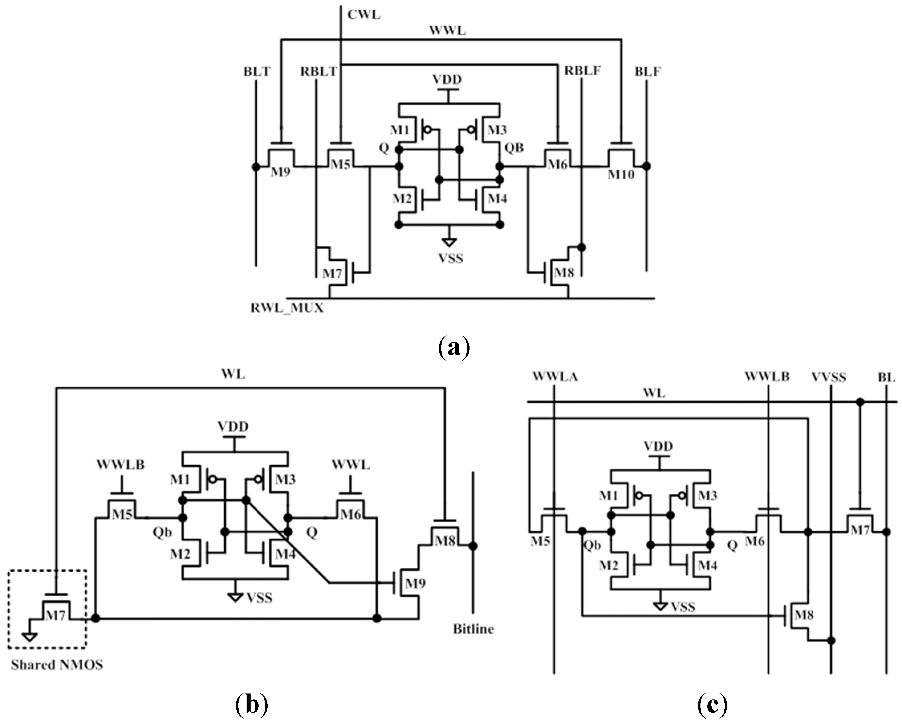
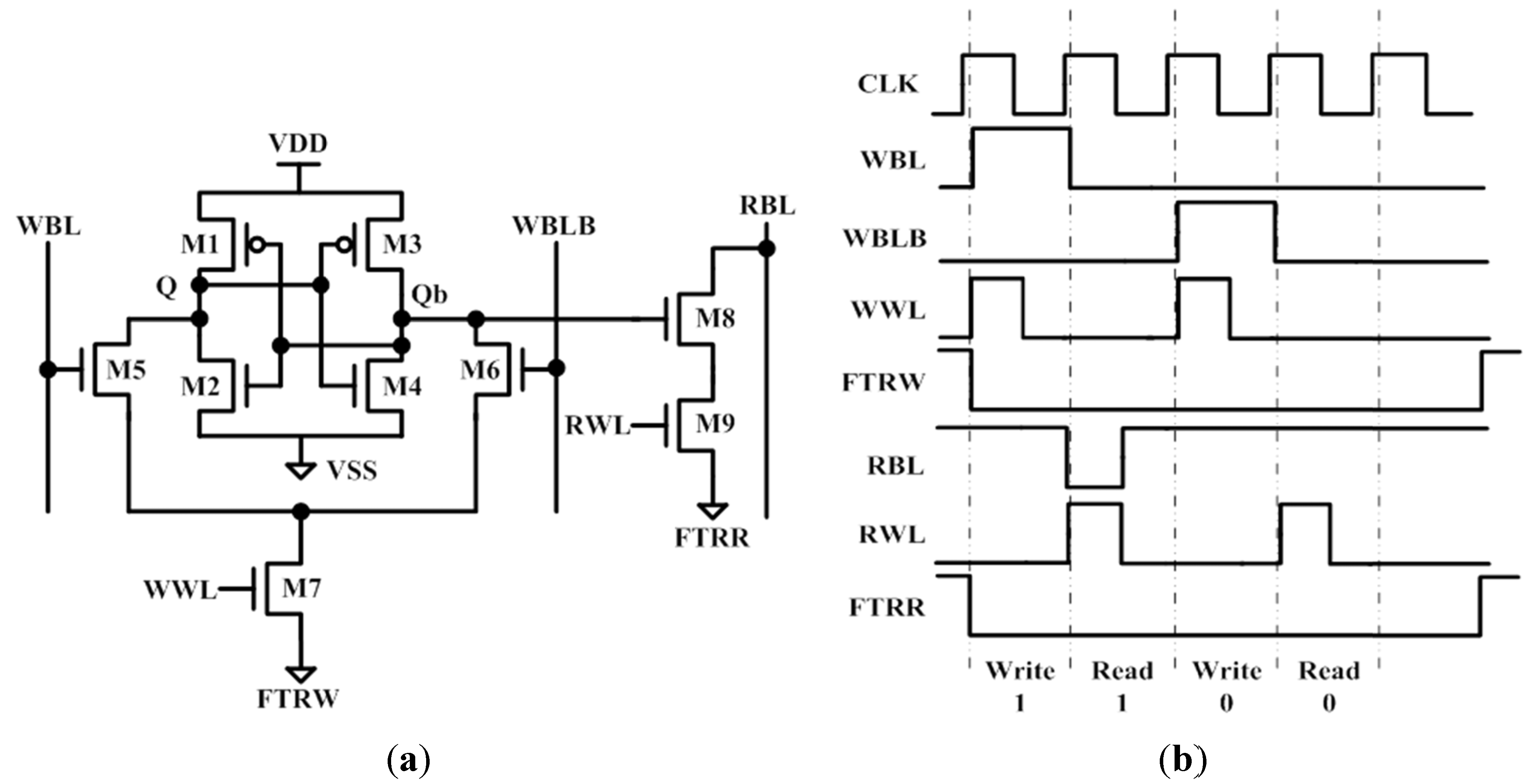
In this section, initially we discuss and compare the results of the energy and delay numbers of the bitcells, and later we move on to the comparisons from energy per operation perspective. In order to do a fair comparison, we size the 6T structures (back-to-back inverters: M1, M2, M3, M4 (Figure 1 and Figure 2) and two NMOS pass transistors: M5 and M6 (Figure 1 and Figure 2) which are the same in all the aforementioned bitcells (WM1, M3 = 0.4u, LM1, M3, M5, M6, M7 = 0.22u, WM2, M4 = 0.28u, LM2, M4, M8, M9 = 0.15u, WM5, M6, M7 = 0.45u). Due to this reason, for all the bitcells under local and global variations we make the µ data retention voltage (DRV) nearly 74 mV, and the µ hold static noise margin (HSNM) roughly equal to 154 mV at the TT_0.4V_27C corner. As the bitcells have different read and write paths, it is hard to size them same with respect to multiple design metrics. However, we tried to make the bitcells’ read and write paths similar. Apart from the M1–M6 being sized the same for all the bitcells, we size the WM8, M9 = 0.36u and LM8, M9 = 0.15u for conventional 8T, this work, and Chiu’s bitcell, WM7, M8 = 0.36u and LM7, M8 = 0.15u for Chang’s, Feki’s and Yang’s bitcell, WM9, M10 = 0.45u and LM9, M10 = 0.22u for Chang’s and Feki’s bitcell, WM7 = 0.45u and LM7 = 0.22u for Chiu’s bitcell and WM7, M8, M9, M10 = 0.16u and L
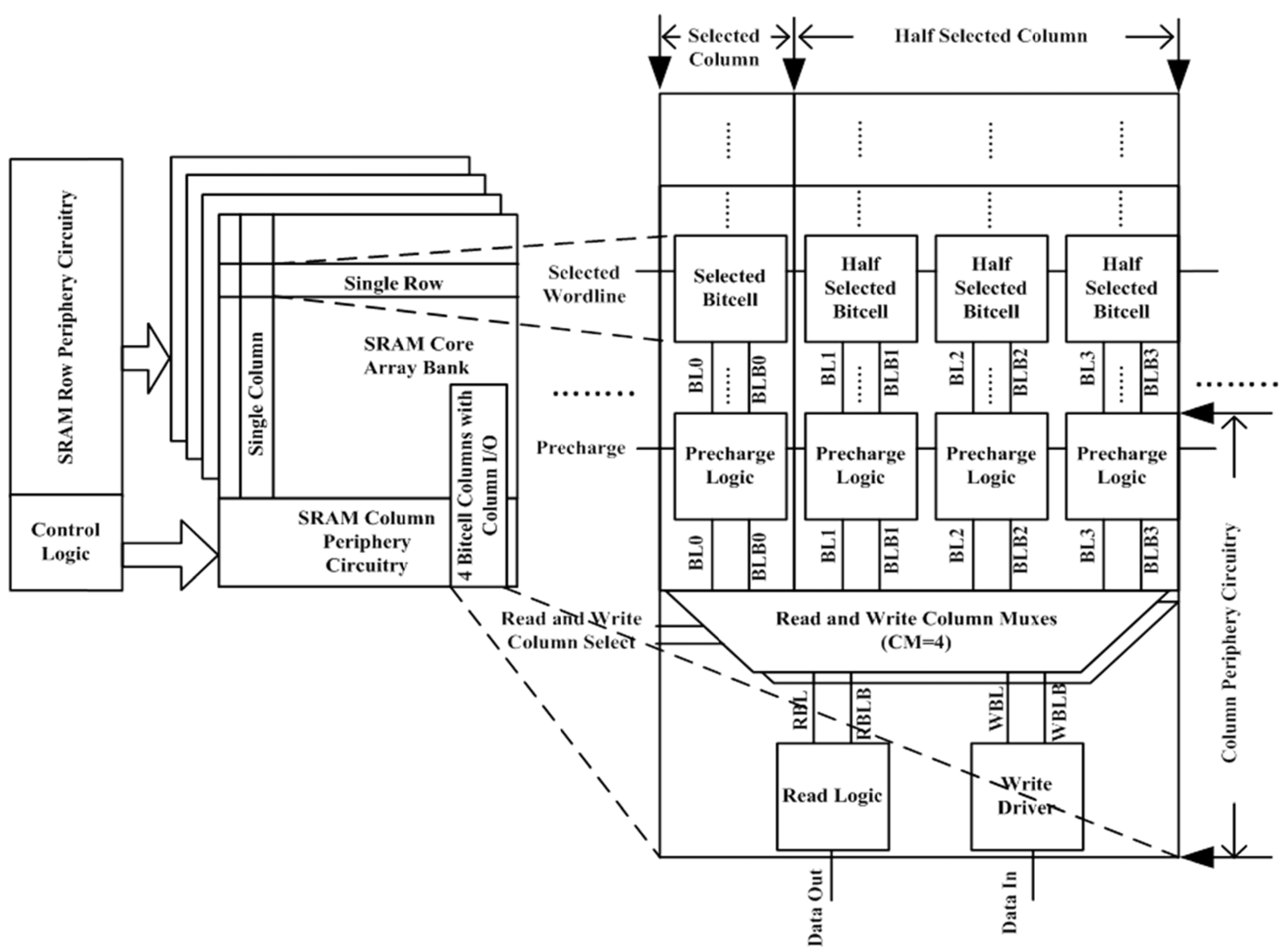
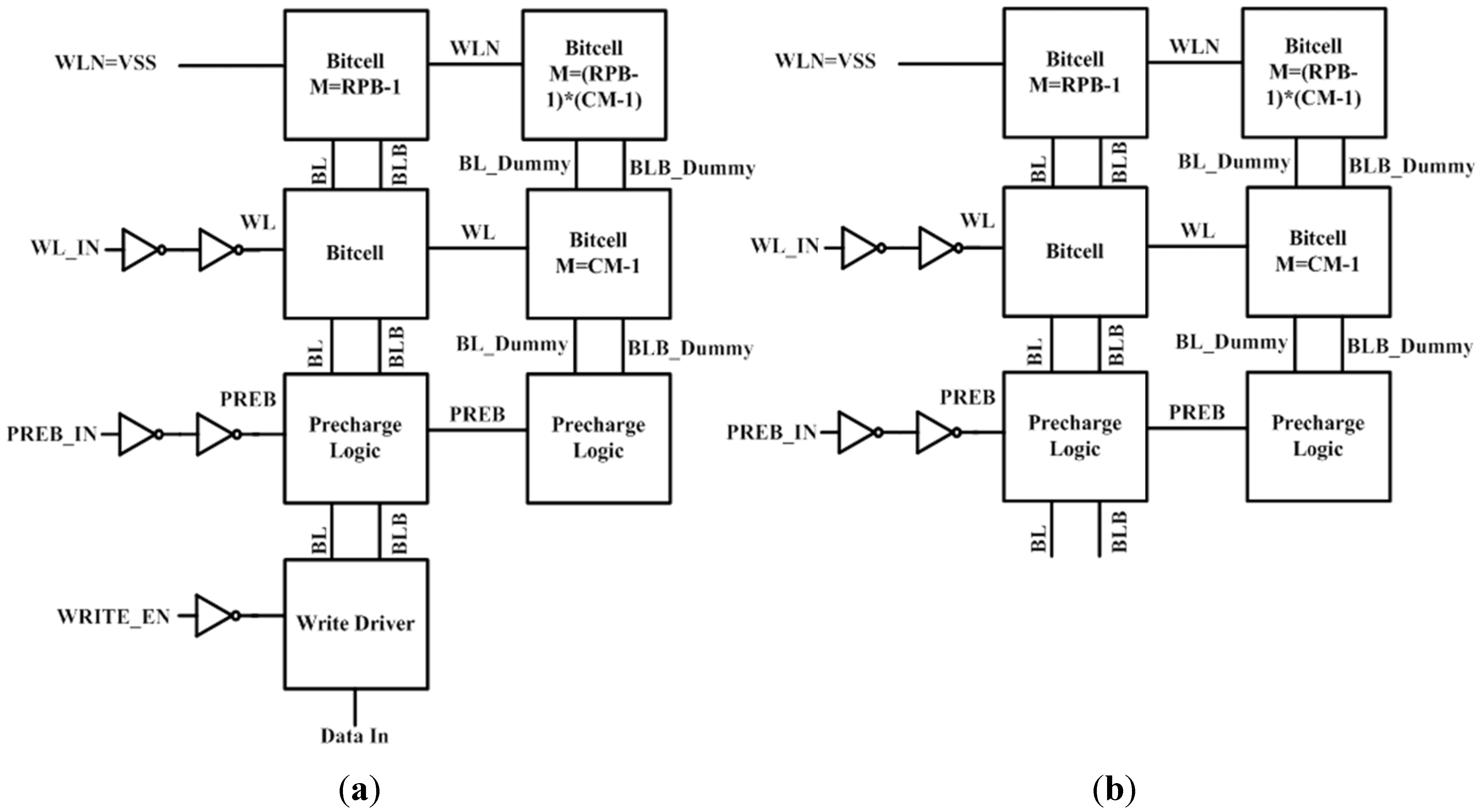
M7, M8, M9, M10 = 0.12u for Kulkarni’s bitcell. For capturing unnecessary energy drainage, we constructed a 4 × 4 modeled array (Figure 6a,b) without the drivers for wordline, etc.) using RPB = 4 and column mux factor (CM) = 4. This model is similar to a 4 × 4 array in the presence of 4:1 column mux, which reveals the dynamic energy loss due to the effect of half-select problem and signal toggling. Comparing with the half-select-free bitcells, the mean read energy of this work is 3.18× lower than Chang’s [7], 2.52× lower than Feki’s [8], 2.05× lower than 8T [10], and 5.6% lower than Yang’s [14]. On the other hand, the mean write energy of this work is 348× lesser than Chang’s [7], 149× lower than Yang’s [14], 1.12× lesser than 8T [10], and 2.4% lower than Feki’s [8] at the TT_0.4V_27C corner with a column mux (CM) 4 in the worst case scenario. We report that the mean leakage current at the same corner is 1.28× lower than the 8T [10] bitcell (Table 1). However, our bitcell has 50% higher read time, and 7× higher write time compared to the conventional 6T at the same corner.
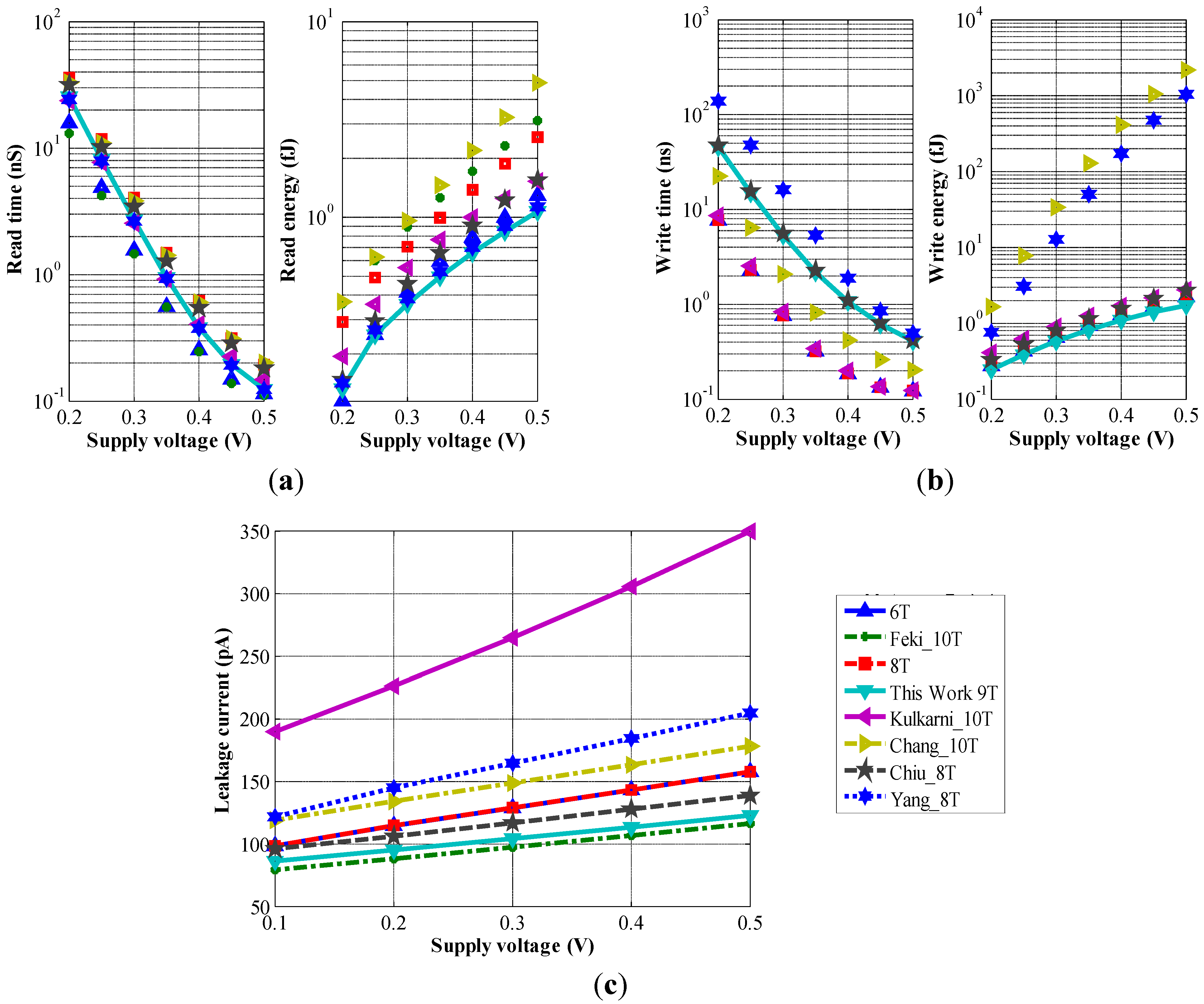
 Figure 7a–c and Table 1 show the comparison of the bitcells across voltages (0.2–0.5 V), and in the presence of statistical variations at the TT_0.4V_27C corner, respectively.
Figure 7. (a) Bitcell read time and total read energy (semi-log scale) vs. supply voltage at TT_27C corner; (b) Bitcell write time and total write energy (semi-log scale) vs. supply voltage at TT_27C corner; (c) Bitcell standby leakage current vs. supply voltage at TT_27C corner.
Jlpea 04 00119 g007
Table 1. Monte Carlo data comparison of bitcell design metrics at TT_0.4V_27C corner (energy in fJ, time in ns and current in pA units).
Metrics6T8T [10]10T [8]10T [6]This work10T [7]8T [9]8T [14]
Read time (μ)0.300.730.280.480.450.690.650.45
Read energy (μ) 0.821.461.791.190.712.260.960.75
Write time (μ)0.190.200.470.261.330.461.393.24
Write energy (μ)1.351.361.241.981.21421.711.69180.67
Leakage current (μ)187.8188.2136.1468.4146.1211.8161.9245.3

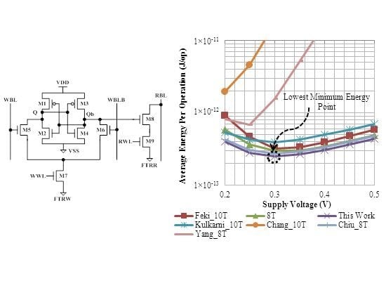
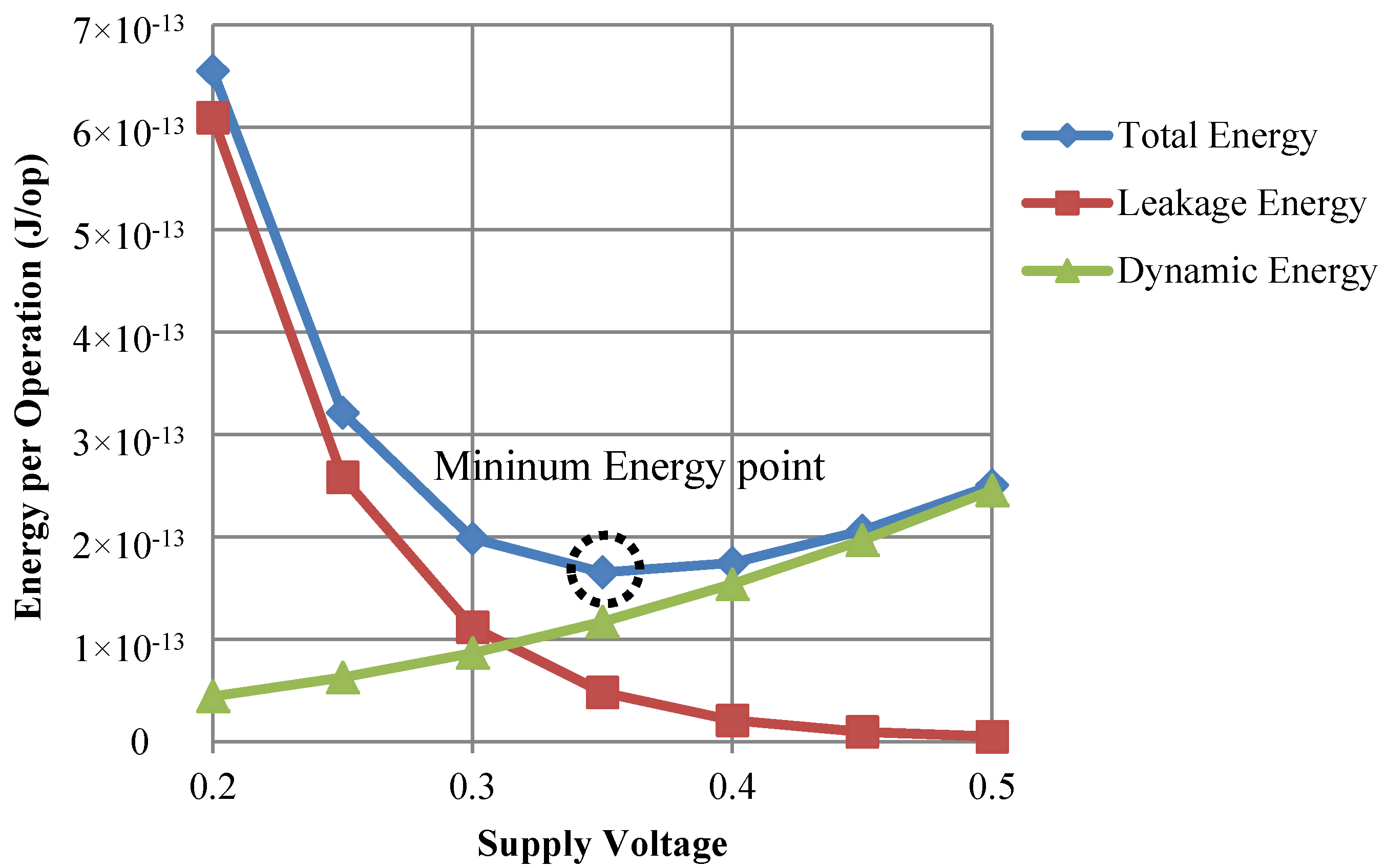
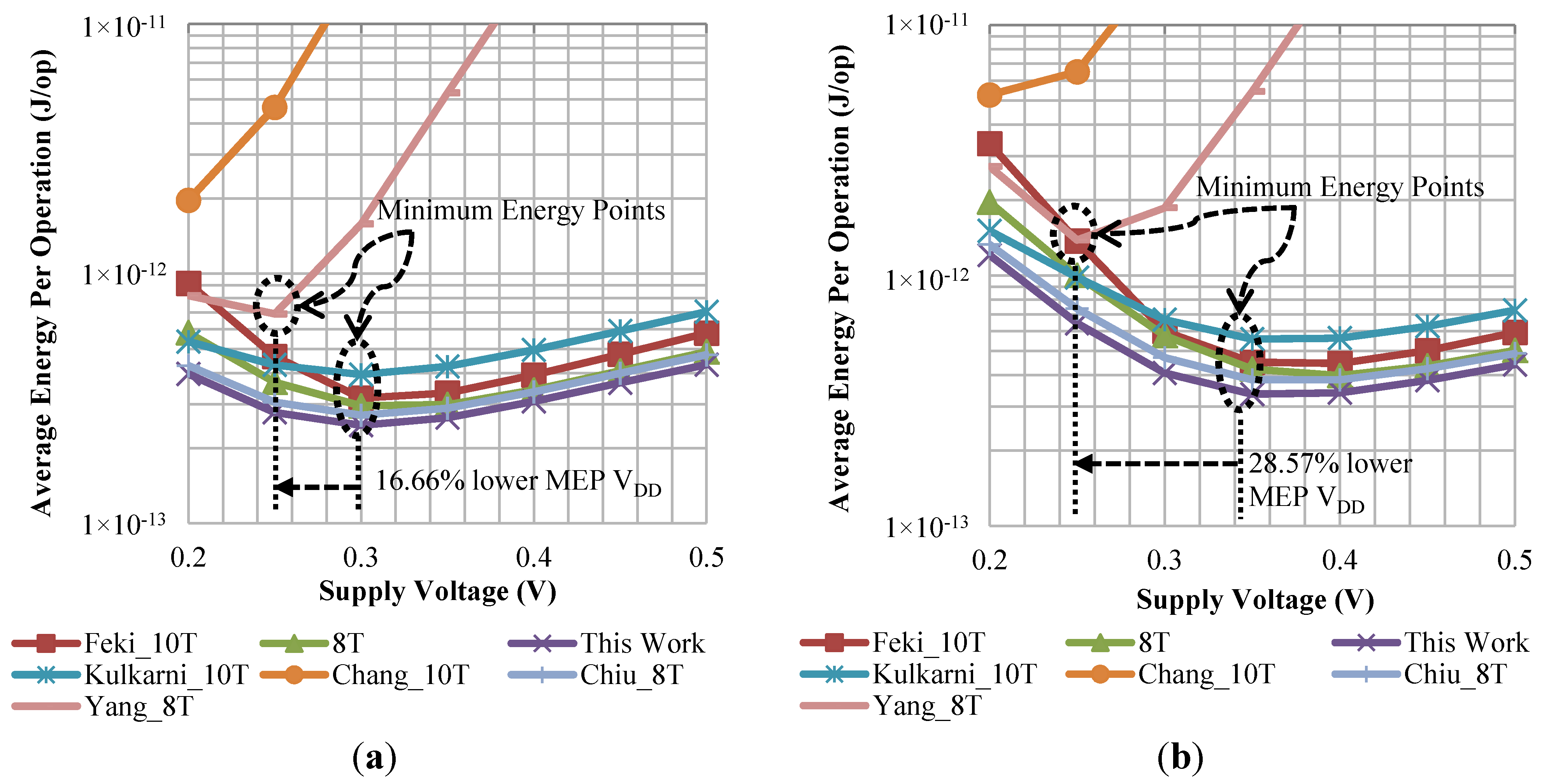
7.1. Comparison of Total Energy per Operation

Figure 8a,b show total energy vs. supply voltage plots and minimum energy points (MEP) for the bitcells with column mux (CM) = 4 and RPB = 16. We generate this plot using the assumption that per four read-write operations, we have three reads and one write, which means that our value of fraction of read and write (Frdwr) is 0.75. We can see that for most of the 8 KB SRAMs, the MEP supply voltage is around 0.3 V, and for most of the 32 KB SRAMs, this MEP supply voltage is around 0.35 V. There are two exceptions to this fact: Chang’s bitcell does not have a minimum energy point within 0.2–0.5 V range in both the cases. This is because Chang’s bitcell has much higher dynamic energy per operation in the subthreshold region compare to the leakage energy per operation than other bitcells (Figure 7a,b). We report 0.2 V as the MEP point for Chang’s bitcell for bigger SRAM macros since it does not have an MEP within the 0.2–0.5 V region. On the other hand, although, Yang’s bitcell has much higher MEP compare to other bitcells, its MEP supply voltage (VDD) is around 0.25 V which is 16.66% lower than most of the bitcells’ MEP VDD (Figure 8a) in 8 KB SRAM and 28.57% lower than most of the bitcells’ MEP VDD (Figure 8b) in 32 KB SRAM.
Figure 8. (a) Total energy vs. supply voltage of 8 KB SRAMs (CM = 4, RPB = 16); (b) Total energy vs. supply voltage of 32 KB SRAMs (CM = 4, RPB = 16).
Jlpea 04 00119 g008

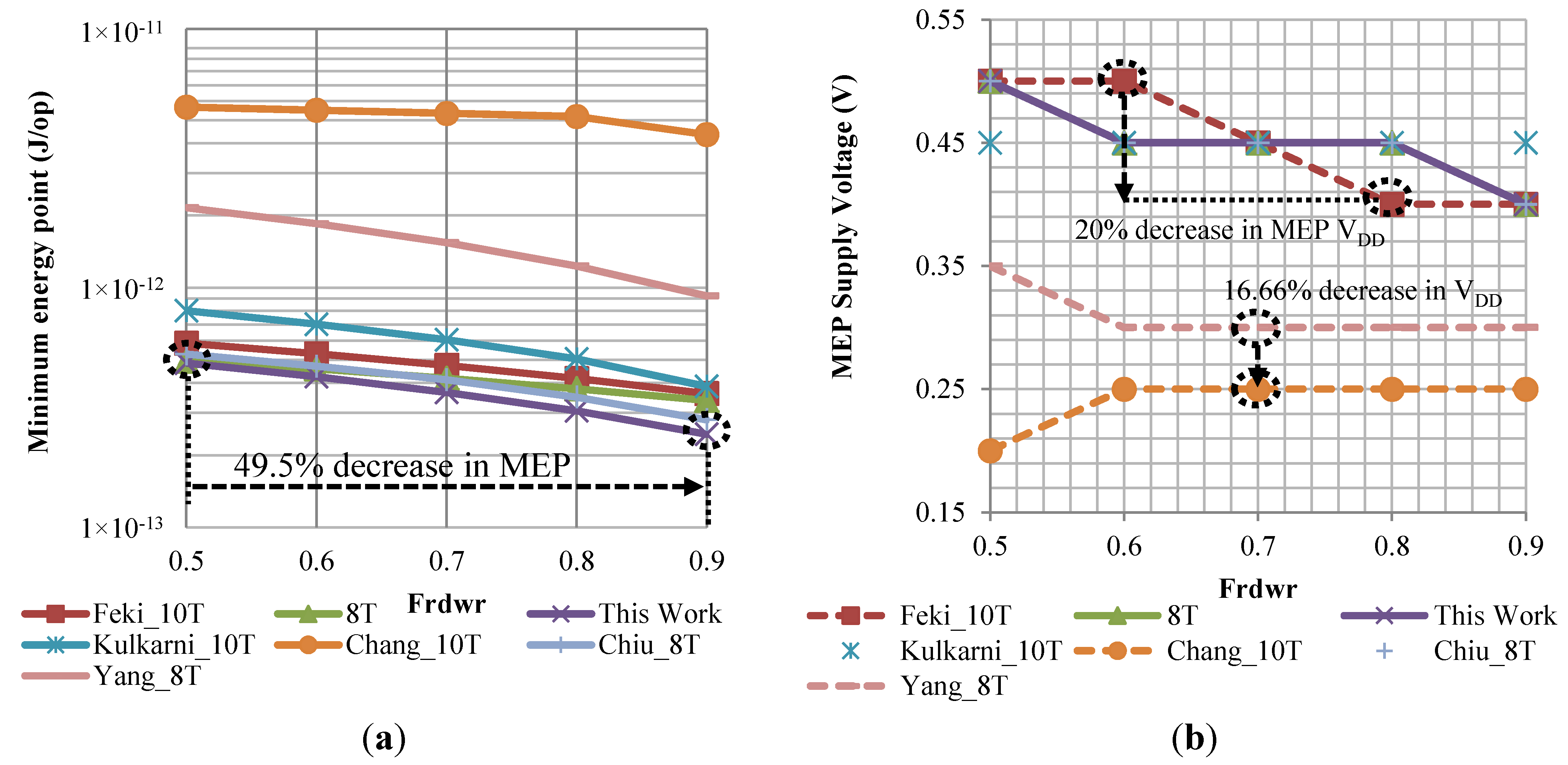
7.2. MEP vs. Fraction of Read and Write and Comparison Results

In order to observe the effect of Frdwr on minimum energy point, we vary the value of Frdwr in Equation (1) and plot the MEP vs. Frdwr and MEP supply voltage vs. Frdwr in Figure 9a,b with CM = 4. We can see that from Figure 9a that increasing the Frdwr results in a decrease in weighted minimum energy points in all bitcells for 32 KB SRAMs with 16 rows per bank (RPB). It is also noticeable that with the increase of Frdwr the slope of the MEP vs. Frdwr changes more or less the same except for Chang’s bitcell, which has much slower slope changes than other bitcells. We report a 49.5% decrease in MEP for this work (Figure 9a) as the Frdwr increases from 0.5 to 0.9. This is because the read energy per operation of this work is much lower than the write energy per operation and weighing more in read energy per operation lowers the weighted MEP point. There is no clear trend observable from the MEP supply voltage vs. Frdwr plot among the bitcells (Figure 9b). However, for Chiu’s and our bitcell, the MEP supply voltage remains constant from Frdwr = 0.6–0.8 at 0.45 V. On the other hand, Yang’s and Chang’s bitcell also shows constant MEP supply voltages across Frdwr = 0.6–0.9. On the contrary, Feki’s bitcell shows a linearly 20% decrease in MEP supply voltage from Frdwr = 0.6–0.8. We also report that Chang’s bitcell has 16.66% lower MEP supply voltage than Yang’s bitcell from Frdwr = 0.6–0.9. From Figure 9a,b, we can say that although Chang’s and Yang’s bitcell has much higher MEP, due to lower MEP supply voltages, it is suitable for bigger subthreshold SoCs having comparable energy per operation with a higher number of logic cells.
Figure 9. (a) Minimum energy point vs. fraction of read and write (Frdwr) for 32 KB SRAM (CM = 4, RPB = 16); (b) MEP supply voltage vs. fraction of read and write (Frdwr) for 32 KB SRAM (CM = 4, RPB = 16).
Jlpea 04 00119 g009

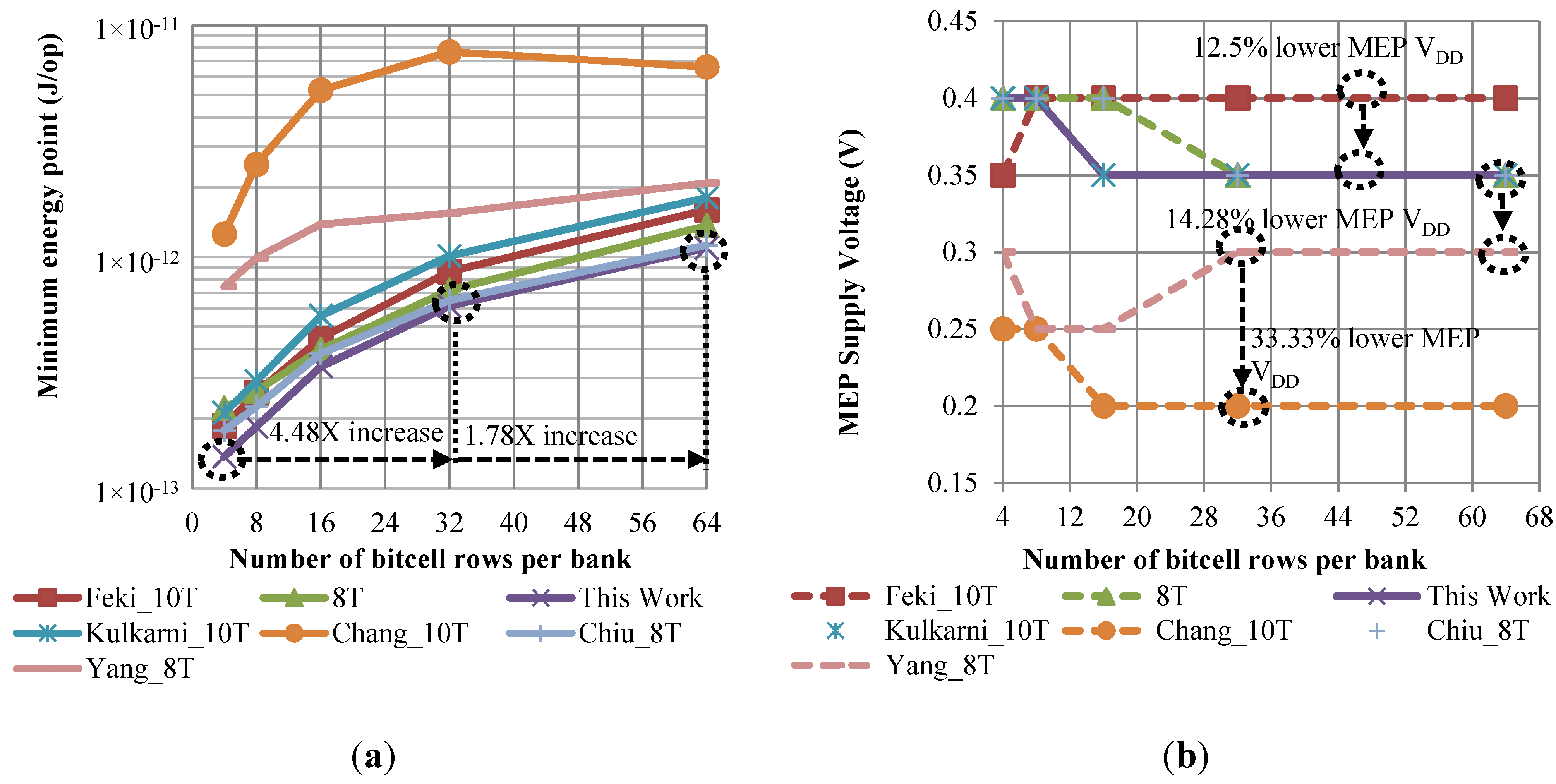
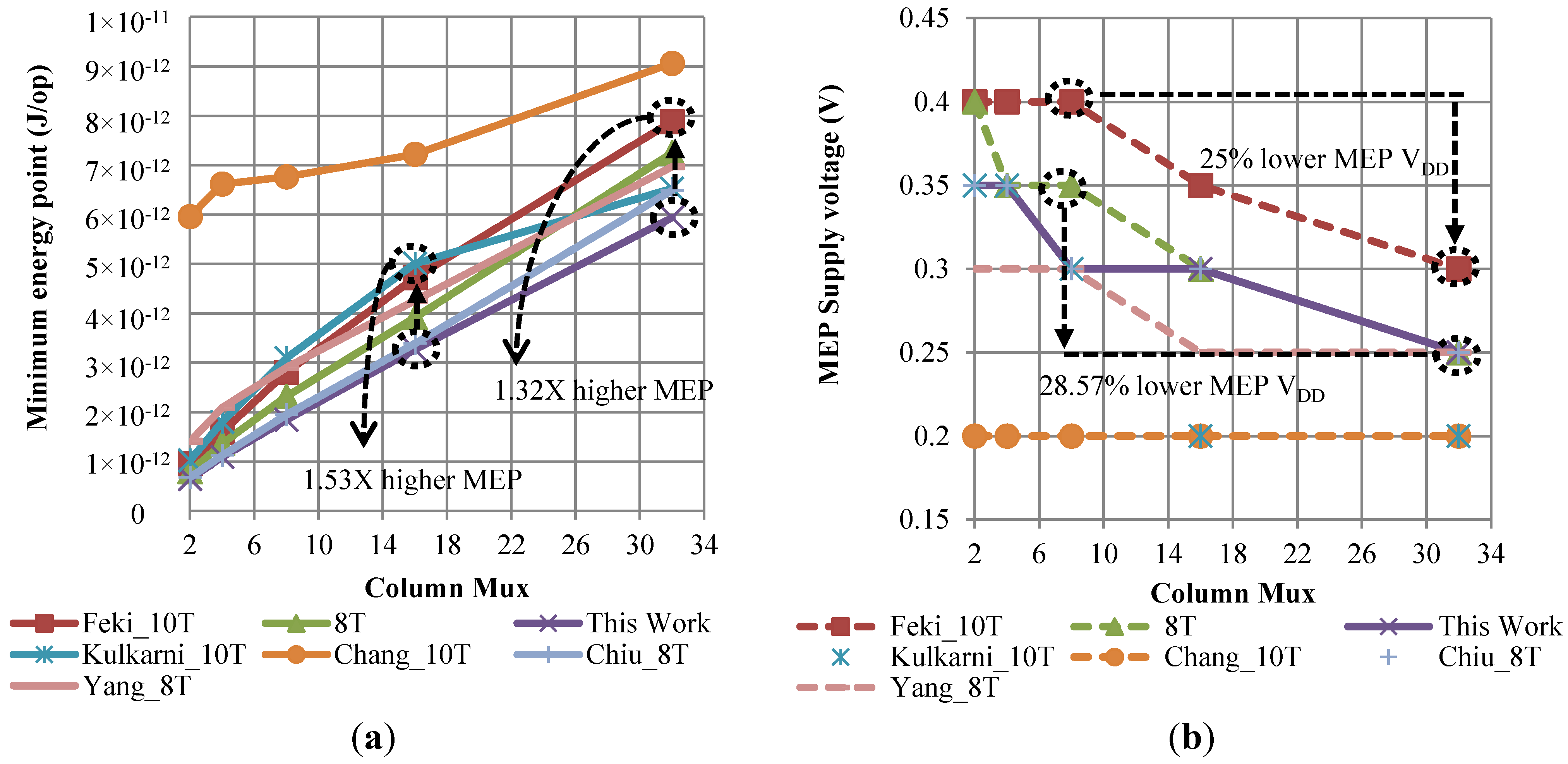
7.3. MEP vs. Number of Bitcell Rows per Bank Comparison Results

Figure 10a shows the variation of MEP with the number of bitcell rows per bank (RPB) for 32 KB SRAMs with CM = 4. This experiment uses a fixed SRAM macro size of 32 KB with word-width being fixed at word-width = 32 in a column mux 4 configuration. In order to keep the SRAM macro size fixed at 32 KB, the bank size and number of banks vary with RPB in this experiment. For the fixed size of 32 KB of SRAM macro size in this experiment, with the increase of RPB, the bank size increases and the number of banks decreases. We can see that all the modeled bitcell macros show a very similar trend of increasing MEP nonlinearly. This work shows minimum MEP variation across RPB = 4 to RPB = 64. However, from RPB = 32 to RPB = 64, Chiu’s bitcell MEP variation is comparable to this work. Within RPB = 16–32, conventional subthreshold 8T and Chiu’s bitcell MEPs are comparable too. We report Feki’s bitcell has 1.46×, 8T has 1.24×, Kulkarni’s bitcell has 1.65×, Chang’s bitcell has 6.05×, Chiu’s has 2.8%, and Yang’s bitcell has 1.9× higher MEP at RPB = 32 for 32 KB SRAM. The modeled macro with our bitcell shows 4.48× and 1.78× increase in MEP for increasing the RPB 8× from RPB = 4–32, and 2X from RPB = 32–64, respectively. We can see a trend in the MEP supply voltage vs. RPB plot shown in Figure 10b for 32 KB SRAM. All the bitcells show constant MEP supply voltage from RPB = 32–64. From RPB = 16–32, Feki’s, Kulkarni’s and Chang’s bitcell maintain their same constant MEP supply voltages as from RPB = 32–64. If we compare the MEP supply voltages of various bitcells above RPB = 32, we can see that Chang’s bitcell has 33.33% lower MEP supply voltage (VDD) than Yang’s bitcell, Yang’s has 14.28% lower MEP VDD than Kulkarni’s, this work and Chiu’s bitcell. On the other hand, our bitcell has 12.5% lower MEP VDD than Feki’s bitcell.
Figure 10. (a) Minimum energy point (MEP) vs. number of bitcell rows per bank (RPB) for 32 KB SRAMs (CM = 4); (b) MEP Supply voltage vs. RPB of 32 KB SRAMs (CM = 4).
Jlpea 04 00119 g010

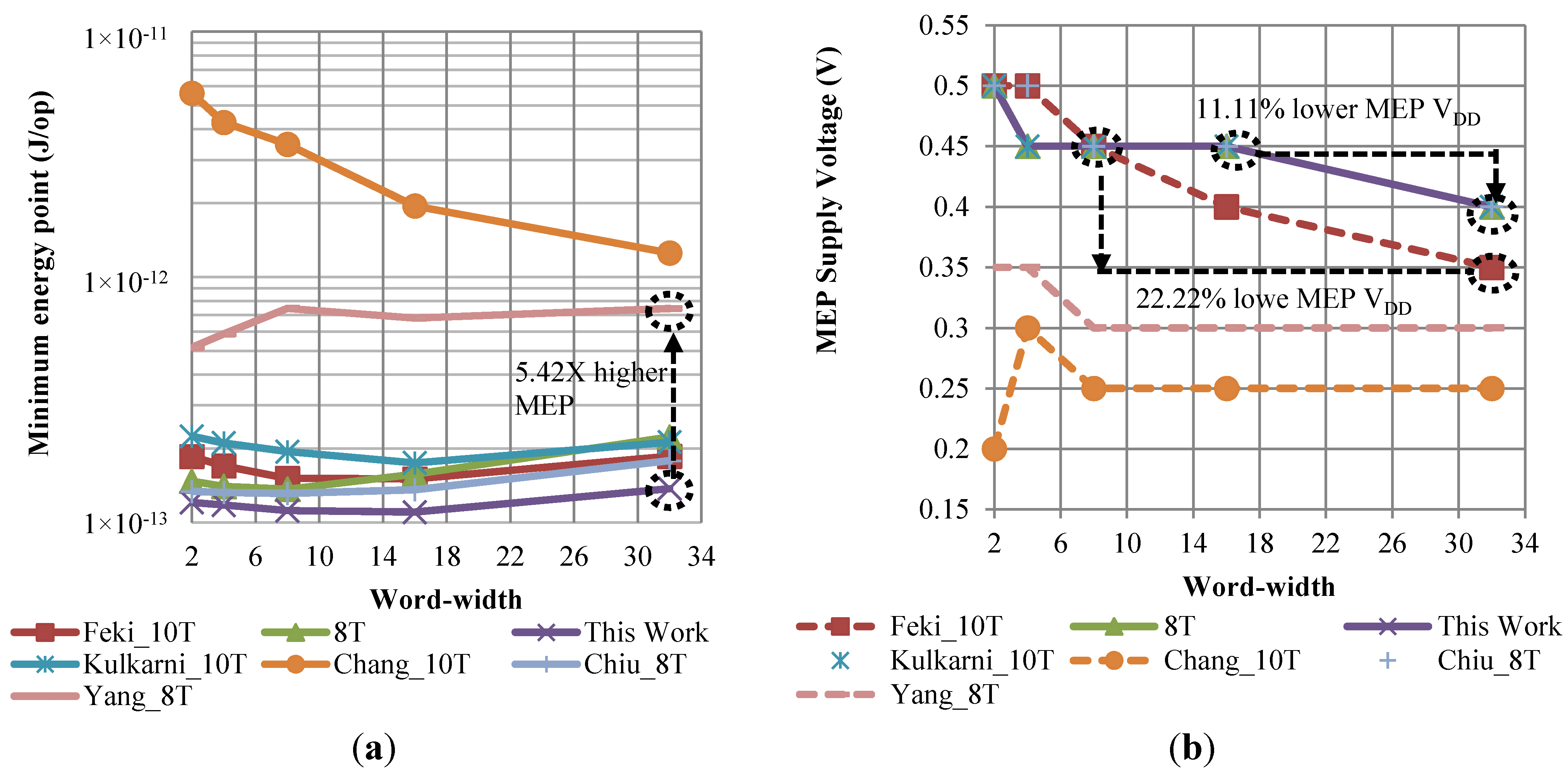
7.4. MEP vs. Word-Width Comparison Results

Figure 11a shows the plot for MEP vs. number of SRAM bits in a word (word-width) for 32 KB SRAMs with CM = 4. We vary the word-width, and RPB at the same time, keeping the size of the banks fixed at 512 bits. Hence, the number of banks remains fixed at 512 for this experiment. In order to keep the bank size constant, the RPB decreases in a bank with the increase in word-width. As RPB and word-width both varies in this experiment with fixed bank size, we see a second order effect in MEP vs. word-width plot (Figure 11a): In almost all the bitcells (except Chang’s and Yang’s), the MEP first decreases and reaches a minimum point at some word-width then again it starts to increase. These minimum MEP points are at word-width = 8 for the 8T and Chiu’s bitcell, and at word-width = 16 for Kulkarni’s and Feki’s bitcells, and this work. It is also, noticeable that our bitcell MEP varies much less than the Chiu’s bitcell with increasing word-width. We report Feki’s bitcell has 1.35×, subthreshold 8T has 1.62×, Kulkarni’s bitcell has 1.55×, Chang’s bitcell has 9.14×, Chiu’s bitcell has 1.3×, and Yang’s bitcell has 5.42× higher MEP than this work for 32 KB SRAMs with word-width = 32 (Figure 11a). Hence, with bigger memory macros, the combination of higher word-width and lower RPB is favorable for subthreshold SRAMs designed with our bitcell. Figure 11b shows the variation of MEP supply voltage vs. word-width. We can see a trend of decreasing MEP VDD for all the bitcells except Chang’s and Yang’s bitcell. For the word-width increase of 4× from word-width = 8–32, Feki’s bitcell shows 22.22% reduction in MEP VDD. On the other hand, Chiu’s and our bitcell show a 11.11% reduction in MEP VDD for a 2× increase in word-width from word-width = 16–32.
Figure 11. (a) Minimum energy point (MEP) vs. word-width (bank size and number of banks kept fixed) for 32 KB SRAMs; (b) MEP supply voltage vs. word-width for 32 KB SRAMs.
Jlpea 04 00119 g011

7.5. MEP vs. Column Mux Comparison Results

Figure 12a shows how the MEP varies with increasing column mux. For this experiment the RPB remains fixed at RPB = 64, the word-width at word-width = 32 and the size of the memory at 32 KB. In order to make the size of the memory constant, with the increase in column mux, the bank size increases and the number of banks decreases. We can see a linear trend of increasing MEP with column mux (CM). However, Kulkarni’s and Chang’s bitcells deviate from this trend in different parts in this plot. From CM = 2–16, although our bitcell MEP is comparable to Chiu’s bitcell MEP, our bitcell MEP gets 9.3% lower than Chiu’s bitcell MEP at CM = 32. We report that Feki’s bitcell has 1.32×, 8T has 1.22×, Kulkarni’s bitcell has 9.8%, Chang’s bitcell has 1.53×, and Yang’s bitcell has 17.36% higher MEP than our bitcell with CM = 32 for 32 KB SRAM macros. In addition, our bitcell shows the lowest MEP over all column mux configurations. For CM = 16, we report that Kulkarni’s bitcell has 1.53× higher MEP than our bitcell as shown in Figure 12a. Figure 12b shows that with increasing column mux factor, the MEP supply voltage decreases with all the bitcell except Chang’s bitcell. As Chang’s bitcell in this memory configuration has lower MEP supply voltage below 0.2 V, we report 0.2 V as its MEP VDD. We report that increasing the mux factor by 8× from CM = 4 to CM = 32, MEP supply voltage decreases by 25% for Feki’s bitcell and 28.57% for conventional 8T as shown in Figure 12b.
Figure 12. (a) Minimum energy point (MEP) vs. column mux (words per row) for 32 KB SRAM; (b) MEP Supply voltage vs. column mux of 32 KB SRAMs.
Jlpea 04 00119 g012

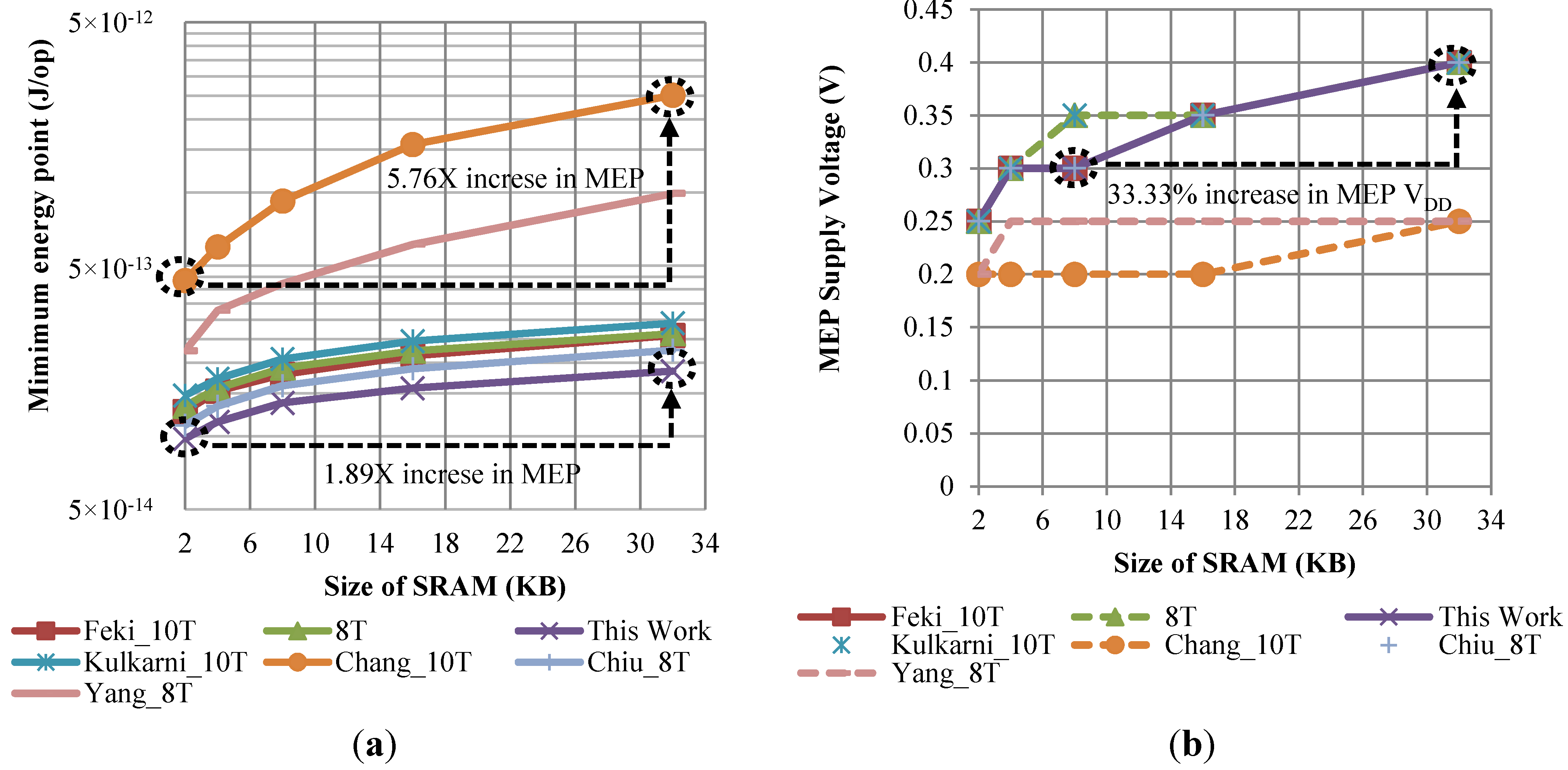
7.6. MEP vs. SRAM Size Comparison Results

Figure 13a shows the variation of MEP with increasing SRAM size with CM = 4. We conduct this experiment with the fixed bank size of 1024 bits per bank, RPB = 8 and word-width = 32 in a column mux 4 scenario. As the size of the SRAM banks remains fixed, the number of banks increases with the increase in memory size. We can see that the MEP of all bitcells increase with increasing SRAM memory size (Figure 13a). This is an expected trend as for a fixed word-width, increasing the SRAM size increases the leakage energy per operation and hence, the MEP shifts to a higher value. However, for this work, it has the lowest MEP across 2–32 KB SRAM memory sizes with RPB = 8. This is consistent with the results of this work’s lower dynamic energy and leakage current data that keeps the MEP for this work lower compare to other bitcell macros. We report that for the SRAM size of 8 KB, Feki’s bitcell has 1.31×, 8T has 1.39×, Kulkarni’s bitcell has 1.51×, Chang’s bitcell has 6.75×, Chiu’s bitcell has 17.54%, and Yang’s bitcell has 3.08× higher MEP than this work. Increasing the SRAM memory size 16× from 2 to 32 KB increases the MEP by only 1.89× for this work, but the other bitcells’ MEP numbers increase by 2.04× for Feki’s bitcell, 1.98× for Kulkarni’s and 8T bitcell, 5.77× for Chang’s bitcell, 2.03× for Chiu’s bitcell, and 4.43× for Yang’s bitcell. Figure 13b shows the variation of MEP supply voltage vs. SRAM macro size. We observe that with the increase in SRAM size, the MEP supply voltage increases for almost all the bitcells. We report a 33.33% increase in MEP supply voltage for Feki’s, Chiu’s, 8T and our bitcell. On the contrary, it is interesting to can see that from 4–32 KB, Yang’s bitcell has a constant MEP supply voltage. Thus, even though Yang’s bitcell has much higher MEP across different SRAM sizes, it can be suitable for bigger subthreshold SoCs having comparable logic energy per operation. However, for smaller low energy biomedical SoCs, our SRAM bitcell shows promising MEP numbers.
Figure 13. (a) Minimum energy point (MEP) vs. SRAM memory size (KB); (b) MEP supply voltage vs. SRAM memory size (KB).
Jlpea 04 00119 g013

8. Conclusions

Across voltages of 0.25–0.5 V, our bitcell [16] has the lowest read energy among [6,7,8,9,10,11,12,13,14,15,16] and the conventional 6T. It has the lowest write energy among the bitcells across the voltages 0.35–0.5 V and second lowest leakage current in the 0.1–0.5 V range. Though our bitcell has lower numbers in energy and leakage current in subthreshold voltages, it suffers from a timing penalty. This work has demonstrated the lowest minimum energy point (MEP) across Frdwr = 0.5–0.9 for 32 KB SRAMs. Our bitcell also provides the lowest MEP variation for 32 KB SRAMs across various rows per bank (RPB) ranging from RPB = 4–64; however, after RPB = 32, Chiu’s bitcell has comparable MEP values for 32 KB SRAMs. This work shows that with varying word-width and fixed bank sizes and number of banks, most of the bitcell has a minima in the MEP curve around word-width = 8 and 16. This is due to a second order effect of varying two of the design knobs word-width and RPB simultaneously. In addition, our bitcell shows the lowest MEP values across word-width = 2–32. However, this work does not compare physical layout area of our bitcell with other bitcells, and therefore, it may have higher area penalty. MEP vs. column mux plots show a linear trend for most of the bitcells, and this work has the lowest MEP values across a mux factor from 2 to 32. Additionally, with RPB = 8, our bitcell has the lowest values of MEP across various SRAM sizes. However, for larger subthreshold SoCs with comparable logic energy per operation, Yang’s and Chang’s bitcells have lower MEP supply voltages, and those may be the best fit from the minimum energy per operation metric standpoint. We conclude that for energy constrained biomedical SoCs, where battery life is critical, operating in the frequency range of a few hundred kHz to several MHz, our 9T half-select-free SRAM bitcell offers lower energy numbers in read and write operations and the lowest MEP values across various subthreshold SRAM design knobs.

Acknowledgments

This project was supported in part by NVIDIA through the DARPA PERFECT program and by the NSF NERC ASSIST Center (EEC-1160483).

Author Contributions

In this research work, author Arijit Banerjee contributed to the literature search and coming up with the idea of the new bitcell that can be more energy efficient from MEP standpoint. He was responsible for simulating all the bitcells for comparison, collecting data from simulations and plotting them in meaningful figures. Arijit also wrote the initial draft version of the paper. Author Dr. Benton H. Calhoun guided Arijit for this research work to choose the research questions and to follow a predefined path for executing this research through technical discussions. He has contributed in this paper by reviewing the trends of the results presented in the paper and proofreading it from technical writing and formatting aspects.

Conflicts of Interest

The authors declare no conflict of interest.

References

  1. Zhang, Y.Q.; Zhang, F.; Shakhsheer, Y.; Silver, J.D.; Klinefelter, A.; Nagaraju, M.; Boley, J.; Pandey, J.; Shrivastava, A.; Carlson, E.J.; et al. A batteryless 19 µW MICS/ISM-band energy harvesting body sensor node SoC for ExG applications. IEEE J. Solid State Circuits 2013, 48, 199–213. [Google Scholar] [CrossRef]
  2. Chen, G.; Fojtik, M.; Kim, D.; Fick, D.; Park, J.; Seok, M.; Chen, M.-T.; Foo, Z.Y.; Sylvester, D.; Blaauw, D. Millimeter-scale nearly perpetual sensor system with stacked battery and solar cells. In Proceedings of the 2010 IEEE International Solid-State Circuits Conference Digest of Technical Papers (ISSCC), San Francisco, CA, USA, 7–11 February 2010; pp. 288–289.
  3. Wang, A.; Chandrakasan, A.P.; Kosonocky, S.V. Optimal supply and threshold scaling for subthreshold CMOS circuits. In Proceedings of the IEEE Computer Society Annual Symposium on VLSI, Pittsburgh, PA, USA, 25–26 April 2002; pp. 5–9.
  4. Wang, A.; Chandrakasan, A. A 180-mV subthreshold FFT processor using a minimum energy design methodology. IEEE J. Solid State Circuits 2005, 40, 310–319. [Google Scholar] [CrossRef]
  5. Seevinck, E.; List, F.J.; Lohstroh, J. Static-noise margin analysis of MOS SRAM cells. IEEE J. Solid State Circuits 1987, 22, 748–754. [Google Scholar] [CrossRef]
  6. Kulkarni, J.P.; Kim, K.; Roy, K. A 160 mV robust schmitt trigger based subthreshold SRAM. IEEE J. Solid State Circuits 2007, 42, 2303–2313. [Google Scholar] [CrossRef]
  7. Chang, I.-J.; Kim, J.J.; Park, S.P.; Roy, K. A 32 kb 10T sub-threshold SRAM array with bit-interleaving and differential read scheme in 90 nm CMOS. IEEE J. Solid State Circuits 2009, 44, 650–658. [Google Scholar]
  8. Feki, A.; Allard, B.; Turgis, D.; Lafont, J.; Ciampolini, L. Proposal of a new ultra low leakage 10T sub threshold SRAM bitcell. In Proceedings of the 2012 International SoC Design Conference (ISOCC), Jeju Island, Korea, 4–7 November 2012; pp. 470–474.
  9. Chiu, Y.-W.; Lin, J.-Y.; Tu, M.-H.; Jou, S.-J.; Chuang, C.-Y. 8T Single-ended sub-threshold SRAM with cross-point data-aware write operation. In Proceedings of the 2011 International Symposium on Low Power Electronics and Design (ISLPED), Fukuoka, Japan, 1–3 August 2011; pp. 169–174.
  10. Verma, N.; Chandrakasan, A.P. A 256 kb 65 nm 8T subthreshold SRAM employing sense-amplifier redundancy. IEEE J. Solid State Circuits 2008, 43, 141–149. [Google Scholar] [CrossRef]
  11. Chandra, V.; Pietrzyk, C.; Aitken, R. On the efficacy of write-assist techniques in low voltage nanoscale SRAMs. In Proceedings of the Design, Automation & Test in Europe Conference & Exhibition (DATE), Dresden, Germany, 8–12 March 2010; pp. 345–350.
  12. Mann, R.W.; Nalam, S.; Wang, J.J.; Calhoun, B.H. Limits of bias based assist methods in nano-scale 6T SRAM. In Proceedings of the 2010 11th International Symposium on Quality Electronic Design (ISQED), San Jose, CA, USA, 22–24 March 2010; pp. 1–8.
  13. Kim, T.; Liu, J.; Keane, J.; Kim, C.H. A high-density subthreshold SRAM with data-independent bitline leakage and virtual ground replica scheme. IEEE J. Solid State Circuits 2008, 43, 518–529. [Google Scholar] [CrossRef]
  14. Yang, H.-I.; Yang, S.-C.; Hsia, M.-C.; Lin, Y.-W.; Chen, C.-C.; Chang, C.-S.; Lin, G.-C.; Chen, Y.-N.; Chuang, C.-T.; Hwang, W.; et al. A high-performance low VMIN 55 nm 512 Kb disturb-free 8T SRAM with adaptive VVSS control. In Proceedings of the 2011 IEEE International SOC Conference (SOCC), Taipei, Taiwan, 26–28 September 2011; pp. 197–200.
  15. Slayman, C. Soft errors—Past history and recent discoveries. In Proceedings of the 2010 IEEE International Integrated Reliability Workshop Final Report (IRW), Stanford Sierra, CA, USA, 17–21 October 2010; pp. 25–30.
  16. Banerjee, A.; Calhoun, B.H. An ultra low energy 9T half-select-free subthreshold SRAM bitcell. In Proceedings of the 2013 IEEE SOI-3D-Subthreshold Microelectronics Technology Unified Conference (S3S), Monterey, CA, USA, 7–10 October 2013; pp. 1–2.
  17. Kim, H.; Kim, S.; van Helleputte, N.; Artes, A.; Konijnenburg, M.; Huisken, J.; van Hoof, C.; Yazicioglu, R.F. A configurable and low-power mixed signal SoC for portable ECG monitoring applications. IEEE Trans. Biomed. Circuits Syst. 2013, 8, 257–267. [Google Scholar] [CrossRef]
  18. Yan, L.; Bae, J.; Lee, S.; Roh, T.; Song, K.; Yoo, H.-J. A 3.9 mW 25-electrode reconfigured sensor for wearable cardiac monitoring system. IEEE J. Solid State Circuits 2011, 46, 353–364. [Google Scholar] [CrossRef]

