Article

A Low Power CMOS Imaging System with Smart Image Capture and Adaptive Complexity 2D-DCT Calculation

Department of Electrical and Computer Engineering, University of Calgary, AB T2N1N4, Canada
*
Author to whom correspondence should be addressed.
J. Low Power Electron. Appl. 2013, 3(3), 267-278; https://doi.org/10.3390/jlpea3030267
Submission received: 4 February 2013 / Revised: 1 June 2013 / Accepted: 29 July 2013 / Published: 8 August 2013
(This article belongs to the Special Issue Energy Efficient Sensors and Applications)

Abstract

:
A novel low power CMOS imaging system with smart image capture and adaptive complexity 2D-Discrete Cosine Transform (DCT) is proposed. Compared with the existing imaging systems, it involves the smart image capture and image processing stages cooperating together and is very efficient. The type of each 8 × 8 block is determined during the image capture stage, and then input into the DCT block, along with the pixel values. The 2D-DCT calculation has adaptive computation complexity according to block types. Since the block type prediction has been moved to the front end, no extra time or calculation is needed during image processing or image capturing for prediction. The image sensor with block type decision circuit is implemented in TSMC 0.18 µm CMOS technology. The adaptive complexity 2D-DCT compression is implemented based on Cyclone EP1C20F400C8 device. The performance including the image quality of the reconstructed picture and the power consumption of the imaging system are compared to those of traditional CMOS imaging systems to show the benefit of the proposed low power algorithm. According to simulation, up to 46% of power consumption can be saved during 2D DCT calculation without extra loss of image quality for the reconstructed pictures compared with the conventional compression methods.

1. Introduction

Wide utilization of portable battery-operated devices in multimedia applications, such as cell phones, portable digital assistants (PDAs) and smart toys, has triggered a demand for ultra low-power image system. CMOS imaging technology has recently become a very attractive solution for these applications as they consume less power, and operate at higher speeds compared with CCD imaging technology [1].
Many low power designs for image capture were reported during the last decade [2,3,4,5,6,7,8]. A review of low power designs in CMOS image sensors at different levels is given in [2]. Some works aim at compensating the reduced signal to noise ratio and dynamic range caused by a low operating voltage [3]. In [4], SOI (Silicon-On-Insulator) technology is used instead of the traditional CMOS technology since it has smaller parasitic capacitance and reduced leakage current. In 2006, the first self powered image sensor was proposed by Fish et al. [5]. Then an optimized energy harvesting CMOS image sensor was proposed [6], where the photodetector itself can be used for power generation besides the PGPd. In [7,8] a block based dual VDD image sensor was proposed. It has dual supply voltages during image capture stage and the supply voltage is decided according to the block types.
After the image capture, energy-aware data compression is usually performed for efficient transmission. The Discrete Cosine Transform (DCT), and in particular the DCT-II, is often used in image/video processing such as JPEG still image compression, MJPEG, MPEG video compression due to its good energy compaction. However the DCT itself contains very computationally intensive matrix multiplications and therefore is power consuming. Numerous algorithms have been proposed attempting to minimize the number of additions and multiplications such as the Loeffler DCT [9,10,11] or even to replace multiplications with only add and shift operations, i.e., Distributed Arithmetic (DA), Coordinate Rotation Digital Computer (CORDIC) and binDCT [12,13,14]. Also, data-dependent DCT algorithms have been introduced for low power purpose [15].
In all the existing CMOS imaging systems, the image capture stage and the compression stage are simply concatenated together. The DCT architectures without multiplier are usually time consuming and hardware-expensive. Some DCT designs subsample the area where pixels change less, but all the block type predictions are made during the digital image processing and require extra processing time and also extra memory space to store the image data during prediction. However, in our imaging system, these two stages are intertwined together. The block type prediction is moved to the front end, that is, the block type is estimated during image capture in an analog way (at the mean time during read out). It is more efficient in terms of power. In addition, no extra time is needed during image processing or image capturing for block type prediction. The 2D DCT calculation has adaptive data format and computation complexity depending on the block type.
The paper is organized as follows. In Section 2, the general algorithm and architecture of the proposed low power imaging system is described. Section 3 discusses the circuit implementation of the imager with the block decision circuit and the adaptive-complexity 2D-DCT. Performance regarding the image quality and the power consumption will be also given in Section 3. Finally, conclusions are presented in Section 4.

2. Proposed Low Power Imaging System with Smart Image Capture and Adaptive Complexity 2D-DCT

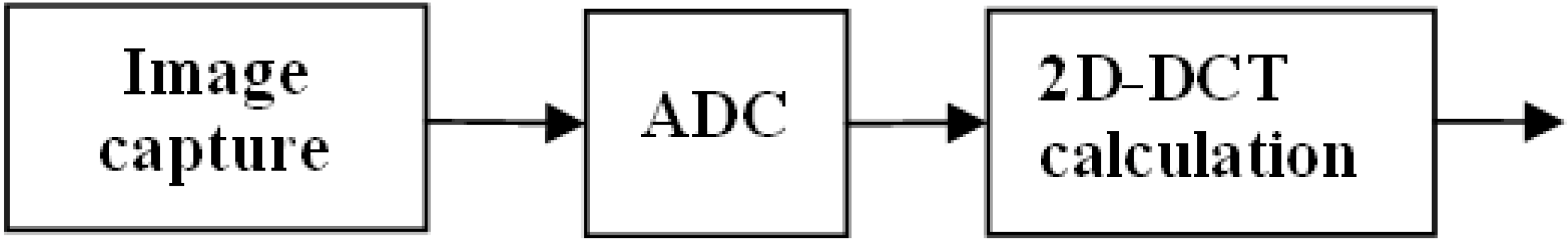
2.1. Traditional CMOS Imaging System with 2D-DCT Calculation

In a traditional CMOS imaging system, the image is first captured by the imager, and then the analog image data go through an Analog-to-Digital (ADC) conversion and then digital processing, such as image compression. The general diagram of a basic traditional digital camera system with 2D-DCT based compression is shown in Figure 1.
Figure 1. A traditional digital imaging system with 2D-Discrete Cosine Transform (DCT) calculation.
Jlpea 03 00267 g001
In hardware the N × N 2D-DCT can be realized by storing the output of the first 1-D DCT in a memory buffer line after line, then applying a second 1-D DCT transform on the columns of the results [16]. N is typically 8 in most of the applications, resulting in an 8 × 8 transform coefficient.

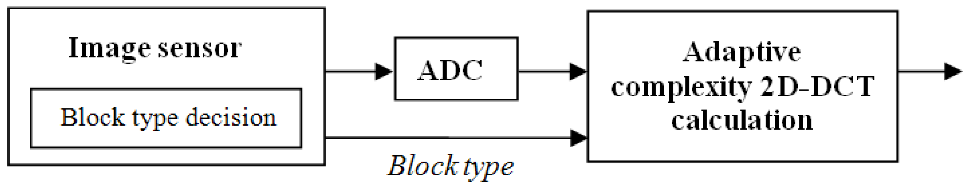
2.2. Proposed Low Power Imaging System with Smart Image Capture and Adaptive Complexity 2D-DCT Calculation

2.2.1. Architecture of the Proposed Low Power Imaging System

The architecture of the novel low power digital camera system with adaptive complexity 2D-DCT based calculation is shown in Figure 2. The system is mainly composed of an image sensor for smart image capture, an ADC for data format converting and an adaptive-complexity 2D-DCT calculation. In addition to capturing images as the traditional CMOS imagers, the image sensor in the proposed camera system contains a block type decision block that can compute the type for each block of 8 × 8 pixels according to the variance [17]. In order to simplify the implementation, we use the difference between the maximum and minimum values within a block as an approximation of the variance to represent how far a set of numbers is spread out, similar to what was done in [8]. A block with lower VmaxVmin has a trend of lower variance. This is more accurate when the variance is small, so we use VmaxVmin as an approximation of the variance to simplify the implementation. The complexity of the proposed 2D DCT calculations is dependent on the block type decided in the image sensor during image capture stage. Power saving is achieved with reduced computation during DCT for small variance blocks.
Figure 2. The proposed low power digital CMOS imaging system with smart image capture and adaptive complexity 2D-DCT calculation.
Jlpea 03 00267 g002

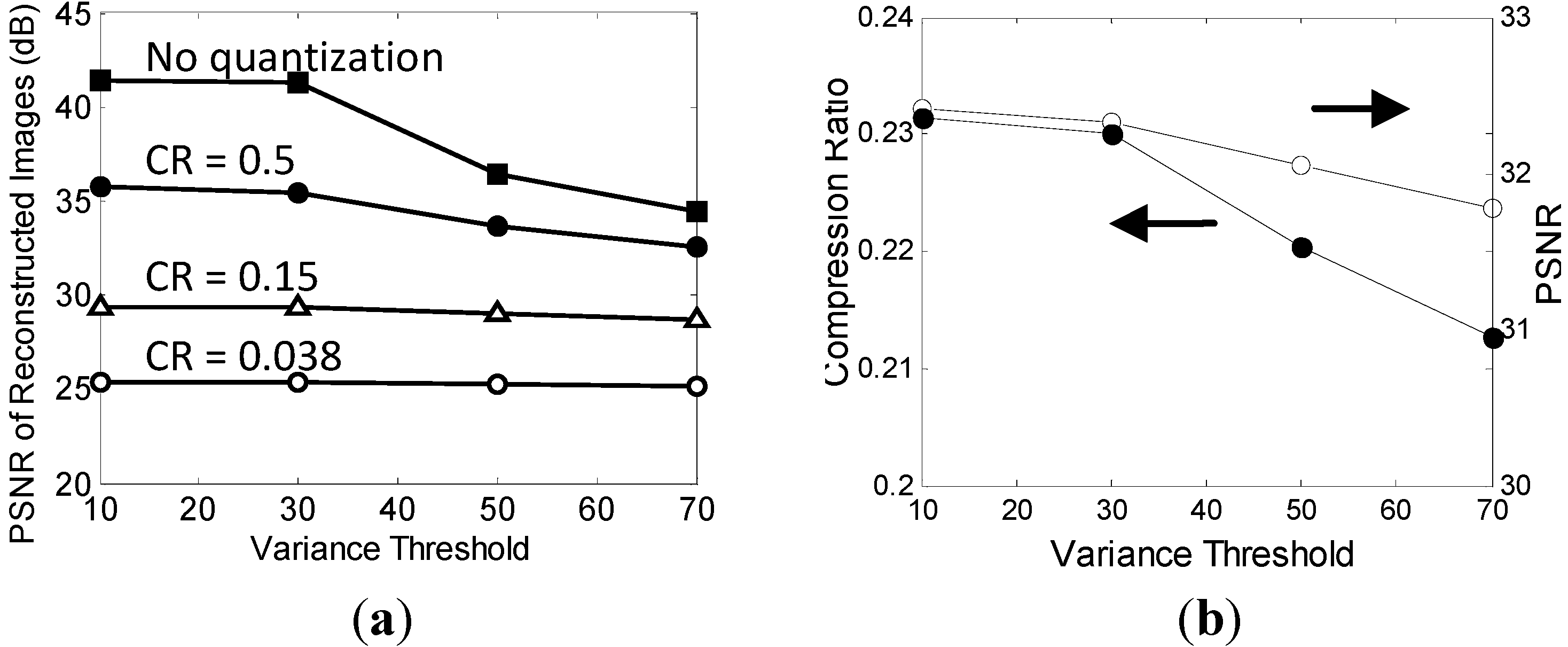
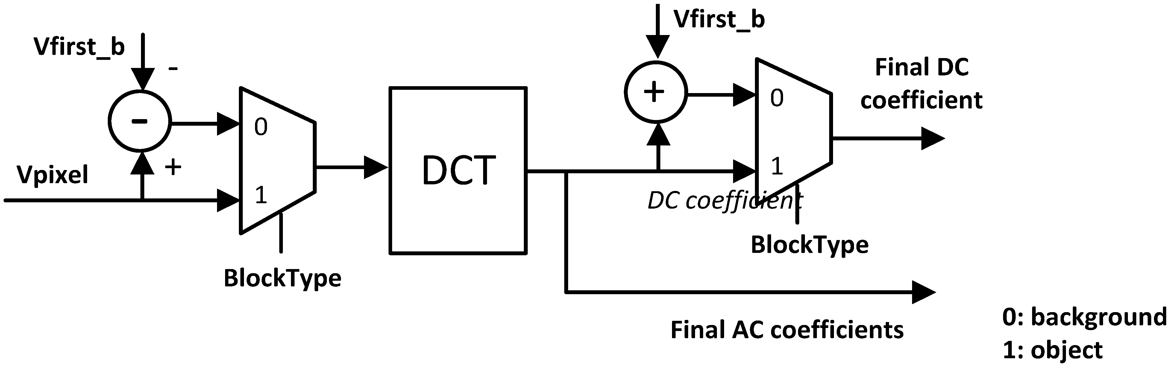
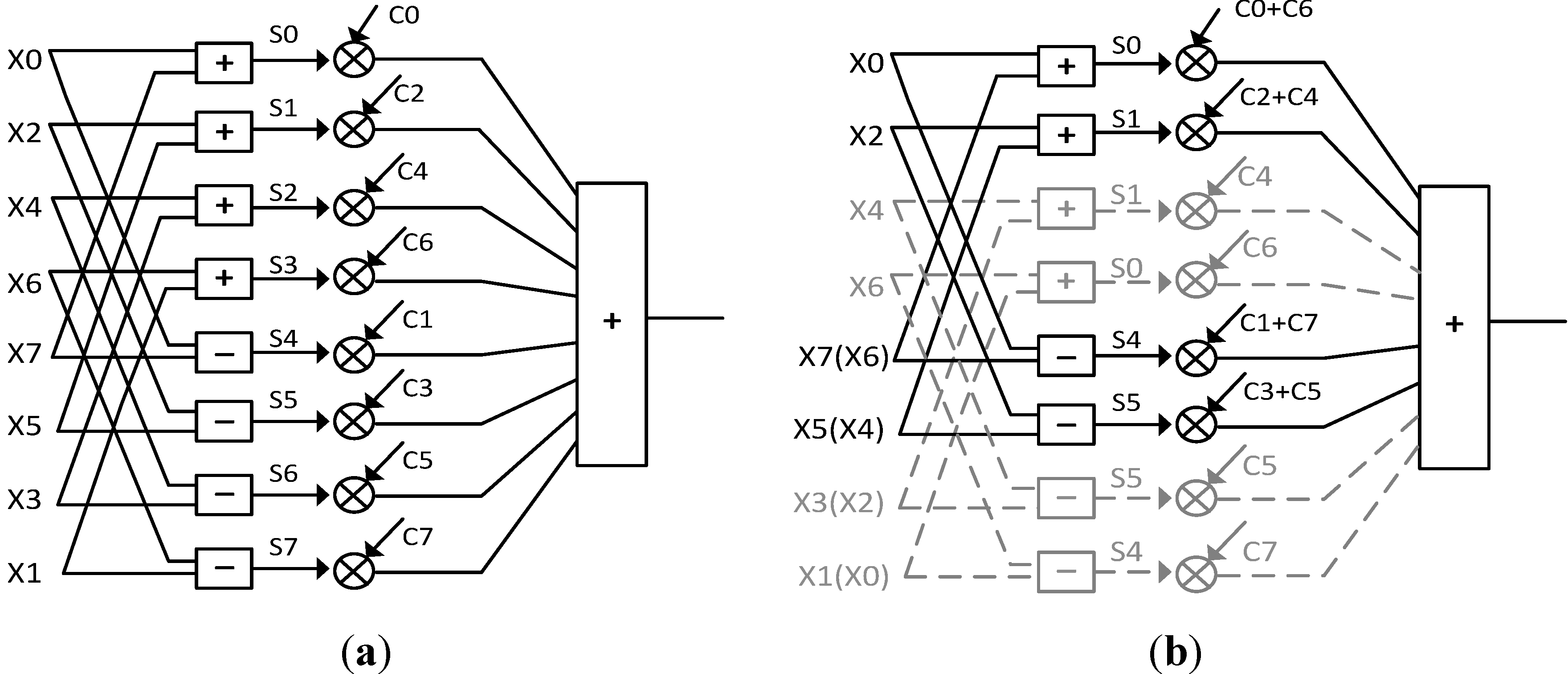
2.2.2. Adaptive Complexity Compression

As shown in Figure 3, for blocks with large VmaxVmin (object blocks), conventional DCT is performed. For the blocks with small VmaxVmin (background blocks), the differential data format is used instead of the pixel value itself during AC coefficients calculation. In addition, the resolution unit is considered as N × N to reduce the computation complexity. Here N can be selected from 1, 2, 4 and 8 according to different applications. In our implementation, N is chosen as 2 for now. With reduced spatial resolution, part of the computation can be skipped without loss of useful information. Because less bits are used during the AC coefficients computing and part of the calculation is skipped, power saving is achieved for background blocks.
Figure 3. Example of the proposed low power algorithm.
Jlpea 03 00267 g003
Using vector form, the 8 × 8 DCT transform becomes F = CXCT. Where X is the input matrix and F is the output results after DCT transform. C is the cosine coefficients matrix and CT is the transpose coefficients matrix.
For background type blocks, the spatial resolution unit will be considered as 2 × 2 during calculation, therefore the row DCT transform becomes F' = CX'CT, where C is the new cosine coefficients and CT is the new transpose coefficients. X' is the new pixel block and F' is the corresponding result after DCT transform.
Jlpea 03 00267 i001
where Jlpea 03 00267 i002
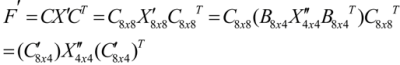
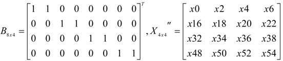
, C'8x4 = C8x8B8x4, and the subscriptions indicate the sizes of the matrixes.
So the matrix sizes during computation can be reduced and the times of multiplication and addition are also reduced. In hardware, it is realized by skipping part of the calculations for background type blocks. Similarly, during column DCT, part of the calculation can also be skipped since half of the inputs in each column are the same.
The analog data are read out from imager row by row. After ADC, the data needs to be stored in a memory temporarily for reordering before performing DCT. If the block type prediction is done during image processing, since the digital data is read out from the memory one by one, at least 64 additional clocks are needed in order to make a prediction for an 8 × 8 block. Also, additional memory is required to keep the data during prediction before DCT is performed. However, in our case, since the block type is decided in the imager during the image capture stage rather than during the image processing stage, it does not need additional processing time. Also the idea of adaptive complexity 2D-DCT can be combined with the dual analog Vdd algorithm proposed in [8], which makes the best of the block type decision circuitry.

3. Implementation of the Low Power Imaging System and Results

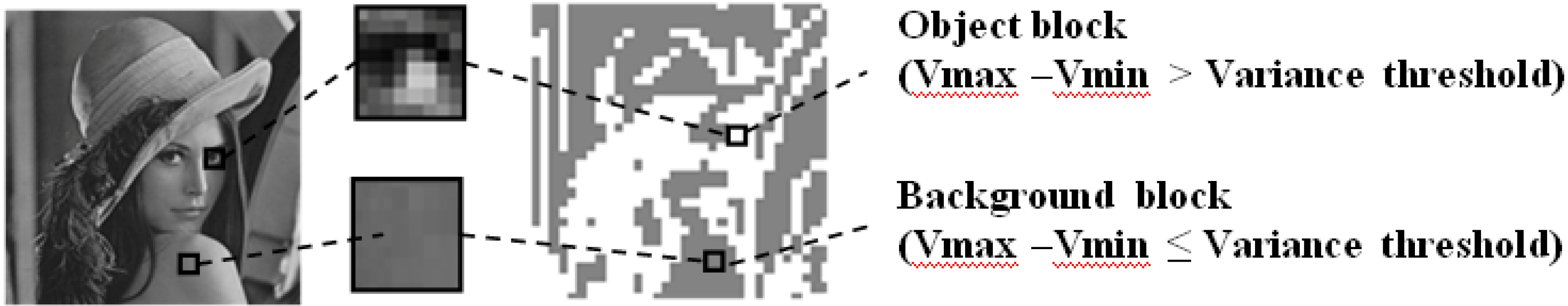
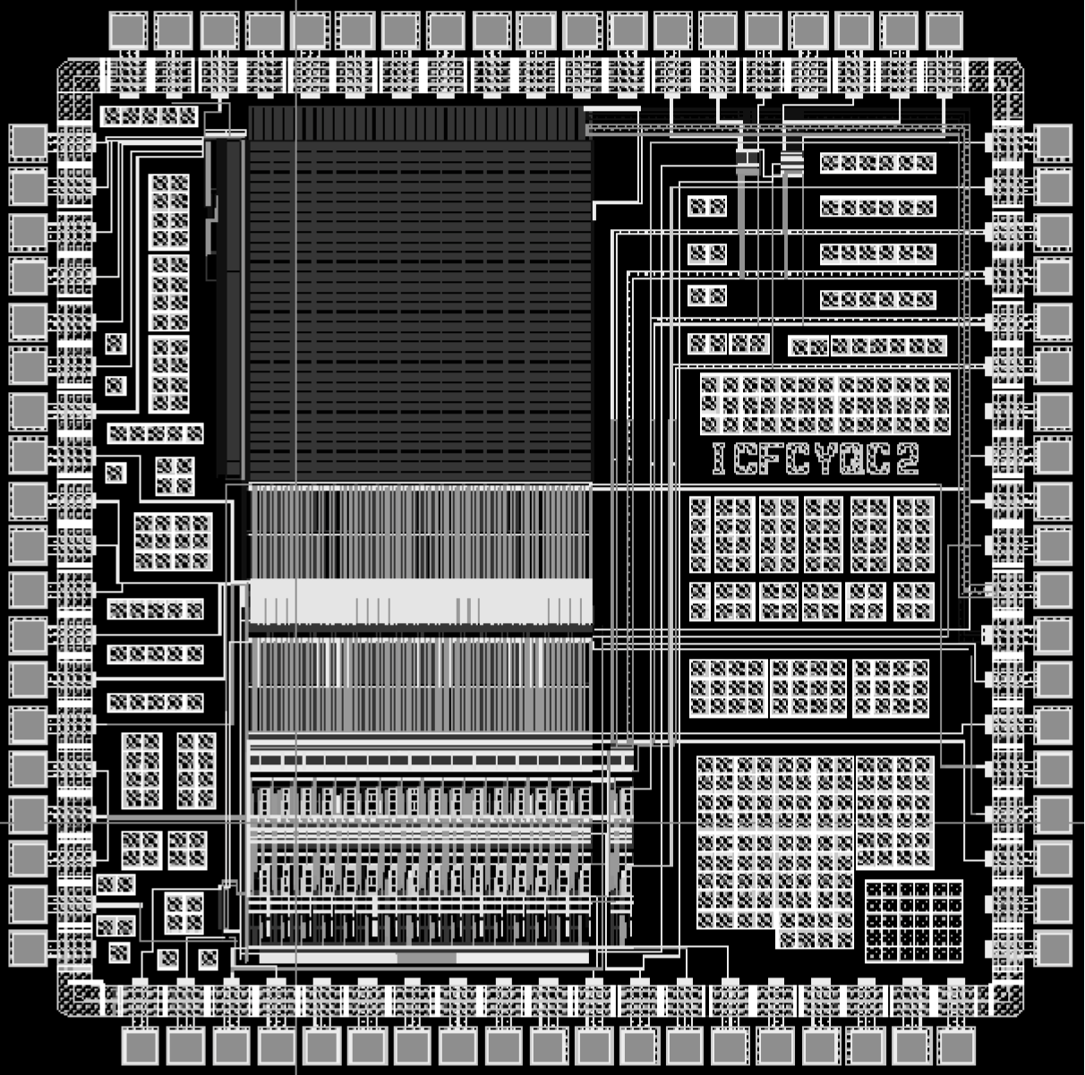
3.1. Image Sensor for Smart Image Capture with Block Type Decision Block

The proposed imager for smart image capture is mainly composed of a pixel array, row and column decoders, block decision block, and readout circuits, as shown in Figure 4. It is similar to the imager proposed in [8] but not exactly the same.
It works in a rolling shutter mode, the signals do not need to be sampled to in-pixel capacitors as required in [8] but to column sample and hold circuit. The readout and the decision operations share the same row select signals and row select transistors. However in [8], the imager works in a global shutter way and the decisions are made at the middle of the integration time, therefore the read out and the decision have separate row select signals and row select transistors. The pixel circuitry here is much simpler than that in [8].
The conventional 3T CMOS APS pixel is used in the pixel array [1]. A p-channel source follower is used to compensate for threshold voltage level-shifting from the n-channel, pixel-level source follower.
Figure 4. Block diagram of the proposed imager for smart image capture.
Jlpea 03 00267 g004
The block type decision unit is shared by each 8 columns and computes the type for each block according to the estimated voltage variance values VMax-VMin, similar to what was done in [8]. The enable signal activates the computations only when needed to save power. The block type decision unit is shown in Figure 4. Detailed description about Winner Take All (WTA), Loser Take All (LTA), Update Max/Min circuitries can be found in [8]. During the readout, the decision signal for each 8 × 8 block is output through a multiplexer one by one to the compression module for adaptive complexity controlling.
A chip for image capture and block type prediction is implemented based on TSMC 0.18 µm process, as shown in Figure 5. Its attributes are given in Table 1. The simulations are done by Cadence Spectre.
Figure 5. Layout of the image sensor with block type decision circuitry.
Jlpea 03 00267 g005
Table 1. Chip Attributes.
TechnologyTSMC 0.18 µm
Voltage supply1.8 V
Pixel array size128 × 128
Pitch width5 µm
Chip size2 mm × 2 mm
Fill factor26%
Estimated power (whole chip)0.5 mW @ 30 FPS
Estimated power (decision logic)7 µW @ 30 FPS

3.2. Image Sensor for Smart Image Capture with Block Type Decision Block Adaptive Complexity 2D-DCT Calculation

2D DCT can be done by running a 1D DCT over every row and then every column. Vector processing using parallel multipliers is a method used for implementation of DCT. The advantages of vector processing method are regular structure, simple control and interconnect and good balance between performance and complexity of implementation. The complexity of the 2D-DCT depends on the block type decided by the image sensor during image capture. Two optimizations are performed for the small variance blocks to save power.

3.2.1. Adaptive Data Format

For small variance blocks, only the differential part of the pixel values Vpixel-VDC are used for AC coefficients computing. Here, the VDC is the minimum value in each corresponding 8 × 8 block. In order to simplify the implementation and reduce the hardware requirement, the first pixel is used as the DC part instead of the minimum pixel in the block.
Figure 6 shows the circuit for implementing the adaptive input format according to block types. For large variance blocks, the pixel values are put for DCT calculation directly. For small variance blocks, the inputs are calculated by subtracting the first pixel value of a block Vfirst_b from the pixel values, and then input to the DCT block. The DC values should be compensated to the DC coefficients to generate the final DC coefficients. Another benefit brought by this optimization is a small increment in image quality of the reconstructed picture. The reason is that because fewer bits are performed for DCT coefficients calculation, less information is lost during the truncation stage. There are less values toggling during DCT coefficient calculation and therefore less power is consumed.
Figure 6. Schematic of adaptive input format according to block types.
Jlpea 03 00267 g006

3.2.2. Adaptive Spatial Resolution
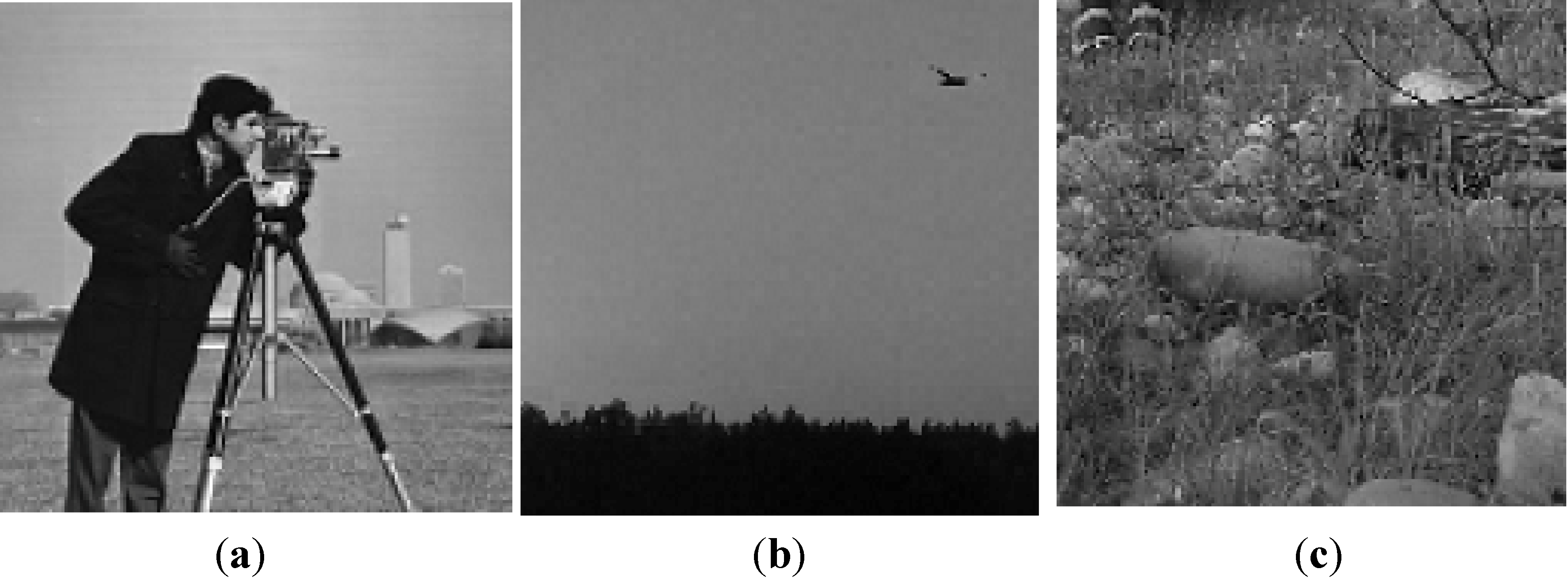
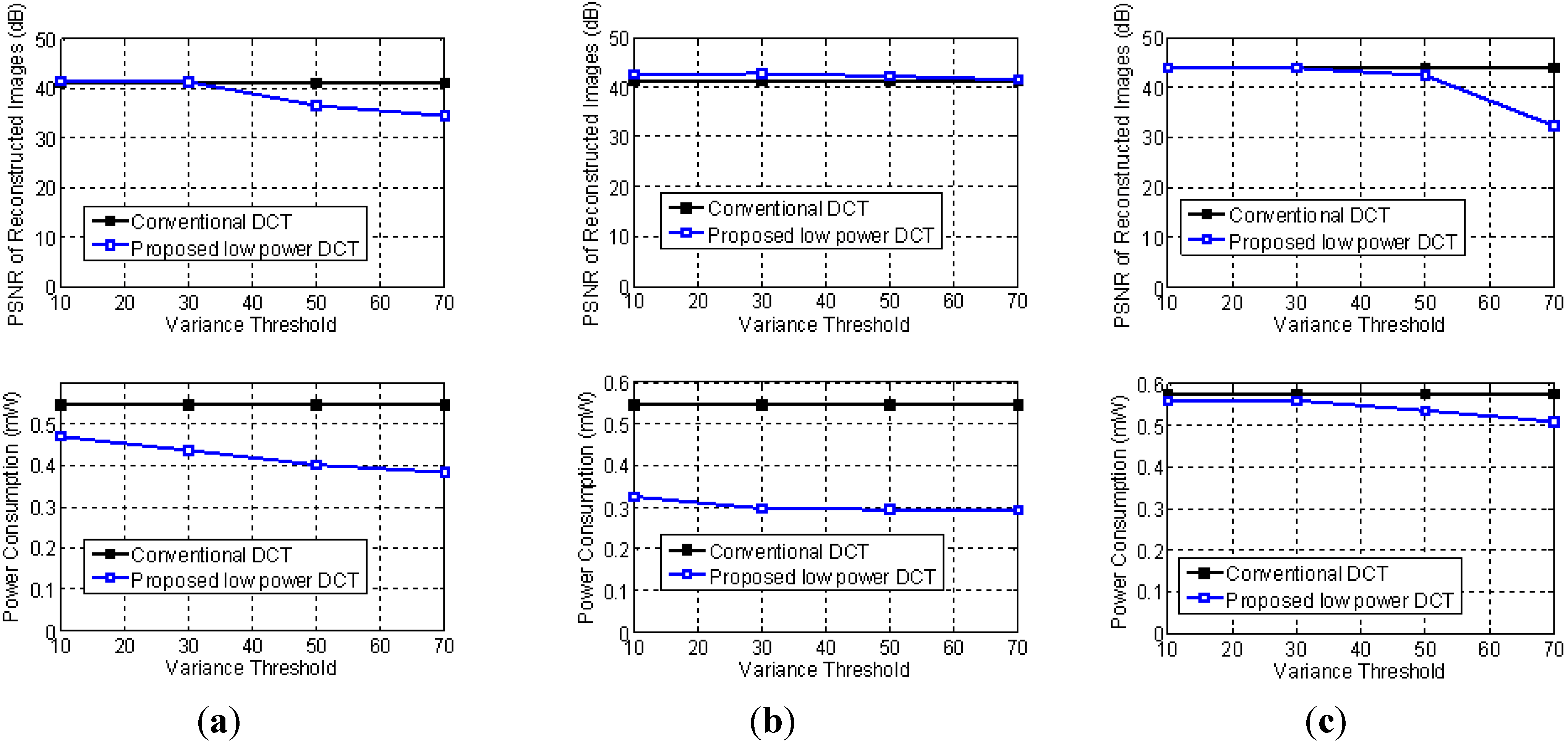
For small variance blocks, the spatial resolution for these blocks can be reduced while not affecting the image quality much. Consequently part of the calculations can be skipped to save power consumption during DCT. For small variance blocks, the calculation for the second row is just the same as the first row, therefore we can skip the row DCT alternatively. In addition, since half of the inputs of the non-skipped row DCT and column DCT are the same, half of the calculation groups can be skipped during calculation for small variance blocks, as shown in Figure 7.
For now, the adaptive complexity 2D-DCT is implemented based on FPGA (Cyclone EP1C20F400C8) first. Later we are planning to integrate the imager for capture and the compression on the same chip. According to the synthesis report given by Quartus II, there is about 10% hardware increase than a conventional 2D-DCT with unique complexity. The maximum frequency is 100 MHz.
Figure 7. Schematic of adaptive spatial resolution according to block types. (a) Normal case—large variance blocks; (b) Low-complexity case (dashed paths are disabled)—Small variance blocks.
Jlpea 03 00267 g007

3.3. Performance

In order to show the benefit of the proposed low power algorithm, the proposed 2D-DCT based computation and a reference 2D-DCT core released by Xilinx [16] are implemented and compared.
As shown in Figure 8, three images of “Camera man”, “Plane” and “Garden” which have background ratio of 50%, 90% and 0.8% small variance block ratios are used to represent three different types of images. The images have 8 bits resolution.
Figure 8. Test images (a) Camera man (background ratio is 50%); (b) Plane (background ratio is 90%); (c) Garden (background ratio is 0.8%).
Jlpea 03 00267 g008
Simulations about the PSNR vs. Variance threshold at different quantization levels are given in Figure 9a. At higher quantization level, the PSNR degradation is smaller. Therefore our low power algorithm is more efficient at higher quantization levels. The worst case happens when there is no quantization performed. The relationship between the Compression Ratio (CR) and variance threshold is given in Figure 9b. Since we have not applied entropy encoding yet, the Compression Ratio (CR) here is expressed by level of the quantization, that is, the percentage of the non-zero coefficients after quantization. The change of the compression ratio is not big since the compression is mainly done by DCT and quantization, the sub sampling by 2 × 2 on background blocks does not add much to the compression ratio. How PSNR changes with the variance threshold also depends on image types. Figure 10 shows the reconstructed image quality and power consumption for different types of images at different variance thresholds compared with those of a traditional compression in worst case (no quantization is performed).
Figure 9. (a) PSNR of reconstructed images vs. Variance threshold at different quantization levels; (b) Compression ratio and PSNR vs. Variance threshold.
Jlpea 03 00267 g009
Figure 10. (a) PSNR and Power vs. Variance threshold for normal background images—Cameraman; (b) PSNR and Power vs. Variance threshold for flat background images—Plane; (c) PSNR and Power vs. Variance threshold for busy background images—Garden.
Jlpea 03 00267 g010
The power is estimated by Quartus II based on the Voltage Change Dump (VCD) files from post layout netlist simulation and the PSNR analysis is done by Matlab. The clock frequency used here is 0.5 MHz corresponding to a 128 × 128 array working at 30 FPS. It can be increased up to 100 MHz for imagers with larger array size and higher frame rate. The power savings varies from image to image. It is more efficient for predominant background images with up to about 46% power saving while no extra image quality degradation is observed compared with traditional compression. Extra image quality degradation is small because optimizations are performed only for background blocks. Power saving and the image quality of the reconstructed picture depend on the variance threshold. It is a tradeoff between image quality and power, and can be easily controlled by the threshold according to different applications. As shown in Table 2, by choosing the appropriate variance threshold, i.e., 30 out of 256 for 8-bit resolution images, significant amounts of power can be saved with no extra image quality degradation.
Table 2. Power saved During 2D-DCT Calculation.
ImagesBackground ratio (th = 30)Percentage of power saving Extra image quality degradation
Garden 0.8%0.5%None
Cameraman 50%24%None
Plane 90%46%None
The power of the whole imaging system is the sum of the image sensor, ADC and the compression. For the proposed image sensor, the power estimation of the block type prediction is 7.0 µW. This adds only about 1.4% to the total imager power, and 0.7% to the system. Therefore, we conclude that the expected power savings outperform the extra power caused by the block type decision circuitry and result in significant power savings for the system.

4. Conclusions

A novel low power CMOS imaging system with smart image capture and adaptive complexity 2D-DCT calculation is proposed, simulated and implemented. The complexity of the 2D-DCT calculation is controlled by the block types which are estimated during image capture stage. It does not add additional processing time or memory space for block type prediction.
The imager is more efficient when the picture has predominant background. By choosing appropriate threshold, up to 46% of the power consumption can be saved during 2D-DCT calculation for images having predominant background, while no extra image quality degradation occurs for the reconstructed pictures compared with traditional compressions. For typical scenarios, up to about 23% of power can be saved for the whole imaging system. The idea of smart image capture and adaptive complexity according to block types can be extended to other 2D DCT architectures.

Acknowledgments

The authors would like to thank CMC for the support with Cadence tools and chip fabrication.

Conflict of Interest

The authors declare no conflict of interest.

References

  1. Yadid-Pecht, O.; Etienne-Cummings, R. CMOS Imagers: From Phototransduction to Image Processing; Kluwer: Norwell, MA, USA, 2004. [Google Scholar]
  2. Fish, A.; Yadid-Pecht, O. Low-Power “Smart” CMOS Image Sensors. In Proceedings of the IEEE International Symposium on Circuits and Systems, Washington DC, USA, 18–21 May 2008; pp. 1408–1411.
  3. Xu, C.; Zhang, W.; Ki, W. A 1.0 V VDD CMOS active-pixel sensor with complementary pixel architecture and pulsewidth modulation fabricated with a 0.25 µm CMOS process. IEEE J. Solid-State Circuits 2002, 37, 1853–1859. [Google Scholar] [CrossRef]
  4. Shen, C.; Xu, C.; Huang, R.; Zhang, W.; Ko, P.K.; Chan, M. A New APS Architecture on SOI Substrate for Low Voltage Operation. In Proceedings of the 9th International Symposium on IC Technology, Systems & Applications, Singapore, 3–5 September 2001; pp. 275–278.
  5. Fish, A.; Hamami, S.; Yadid-Pecht, O. CMOS image sensors with self-powered generation capability. IEEE Trans. Circuits Syst. II 2006, 53, 131–135. [Google Scholar]
  6. Shi, C.; Law, M.K.; Bermak, A. A novel asynchronous pixel for an energy harvesting CMOS image sensor. IEEE Trans. VLSI Syst. 2011, 19, 118–129. [Google Scholar] [CrossRef]
  7. Gao, Q.; Yadid-Pecht, O. Dual VDD Block Based CMOS Image Sensor–Preliminary Evaluation. In Proceedings of the IEEE International Symposium on Circuits and Systems (ISCAS), Rio de Janeiro, Brazil, 15–19 May 2011; pp. 1820–1823.
  8. Gao, Q.; Yadid-Pecht, O. A low power block based CMOS image sensor with dual VDD. IEEE Sens. J. 2012, 12, 747–755. [Google Scholar] [CrossRef]
  9. Loeffler, C.; Lightenberg, A.; Moschytz, G.S. Practical Fast 1-D DCT Algorithms with 11-Multiplications. In Proceedings of the International Conference on AcousticsSpeechand Signal Processing-89, Glasgow, UK, 23–26 May 1989; Volume 2, pp. 988–991.
  10. Thoudam, V.P.S.; Bhaumik, B.; Chatterjee, S. Ultra Low Power Implementation of 2-D DCT for Image/Video Compression. In Proceedings of International Conference on Computer Applications & Industrial Electronics (ICCAIE 2010), Kuala Lumpur, Malaysia, 5–7 December 2010; pp. 532–536.
  11. Sun, C.-C.; Ruan, S.-J.; Heyne, B.; Goetze, J. Low-power and high-quality Cordic-based Loeffler DCT for signal processing. Circuits Devices Syst. IET 2007, 1, 453–461. [Google Scholar] [CrossRef]
  12. Tran, T.D. The binDCT: Fast multiplierless approximation of the DCT. IEEE Signal Process. Lett. 2000, 7, 141–144. [Google Scholar] [CrossRef]
  13. Sung, T.-Y.; Shieh, Y.-S.; Yu, C.-W.; Hsin, H.-C. High-Efficiency and Low-Power Architectures for 2-D DCT and IDCT Based on CORDIC Rotation. In Proceedings of the 7th International Conference on Parallel and Distributed ComputingApplications and Technologies, Taipei, Taiwan, 4–7 December 2006; pp. 191–196.
  14. Jeong, H.; Kim, J.; Cho, W.-K. Low-power multiplierless DCT architecture using image data correlation. IEEE Trans. Consum. Electron. 2004, 50, 262–267. [Google Scholar] [CrossRef]
  15. Xanthopoulos, T.; Chandrakasan, A.P. A low-power DCT core using adaptive bitwidth and arithmetic activity exploiting signal correlations and quantization. IEEE J. Solid-State Circuits 2000, 35, 740–750. [Google Scholar] [CrossRef]
  16. Pillai, L. Video Compression Using DCT; Xilinx: San Jose, CA, USA, 2002. [Google Scholar]
  17. Loeve, M. Probability Theory, Graduate Texts in Mathematics, 4th ed.; Springer-Verlag: Berlin, Germany, 1977. [Google Scholar]

