Reconfigurable Threshold Logic Gates using Memristive Devices


Abstract
:1. Introduction
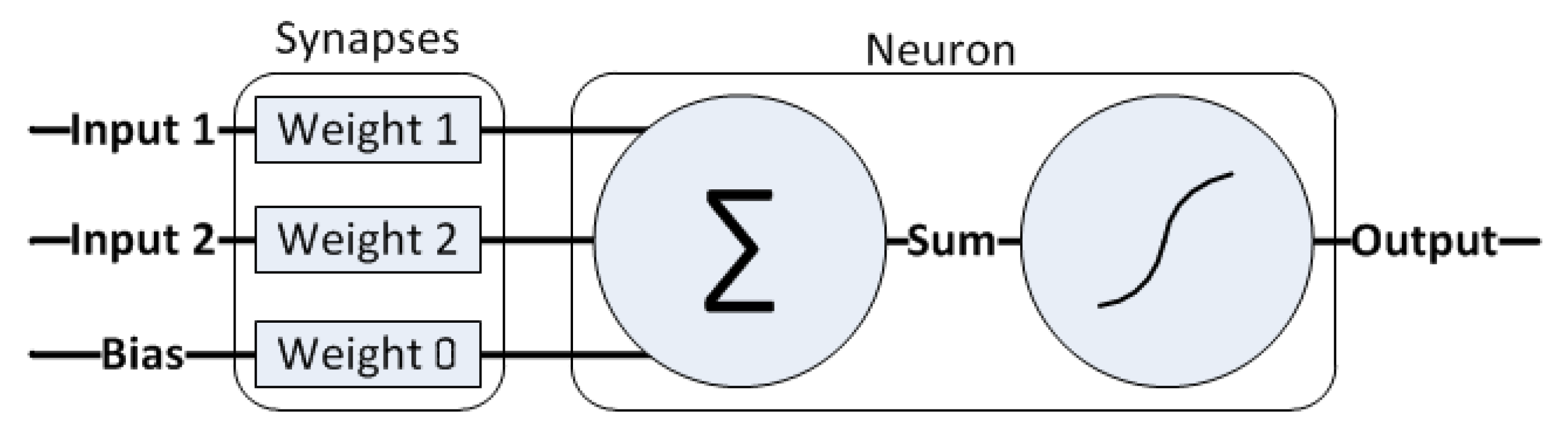
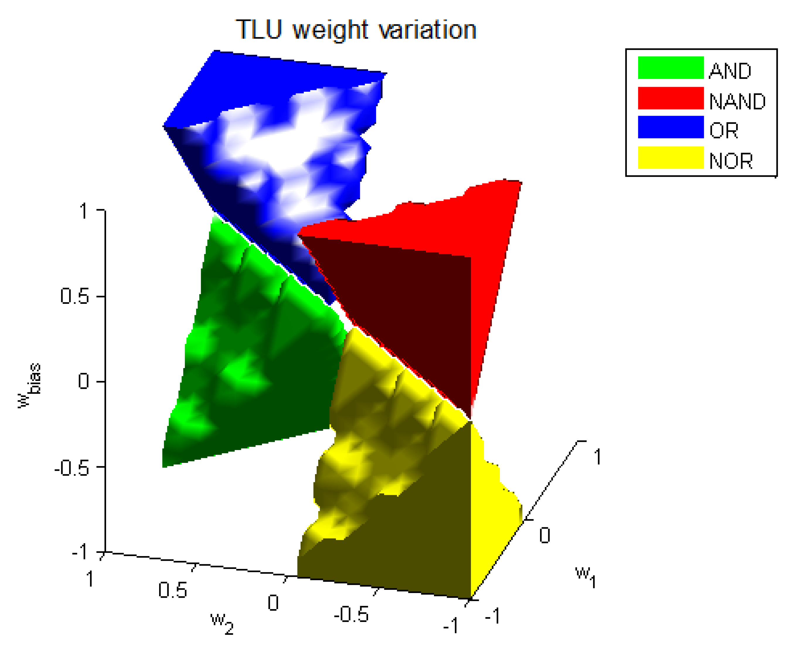
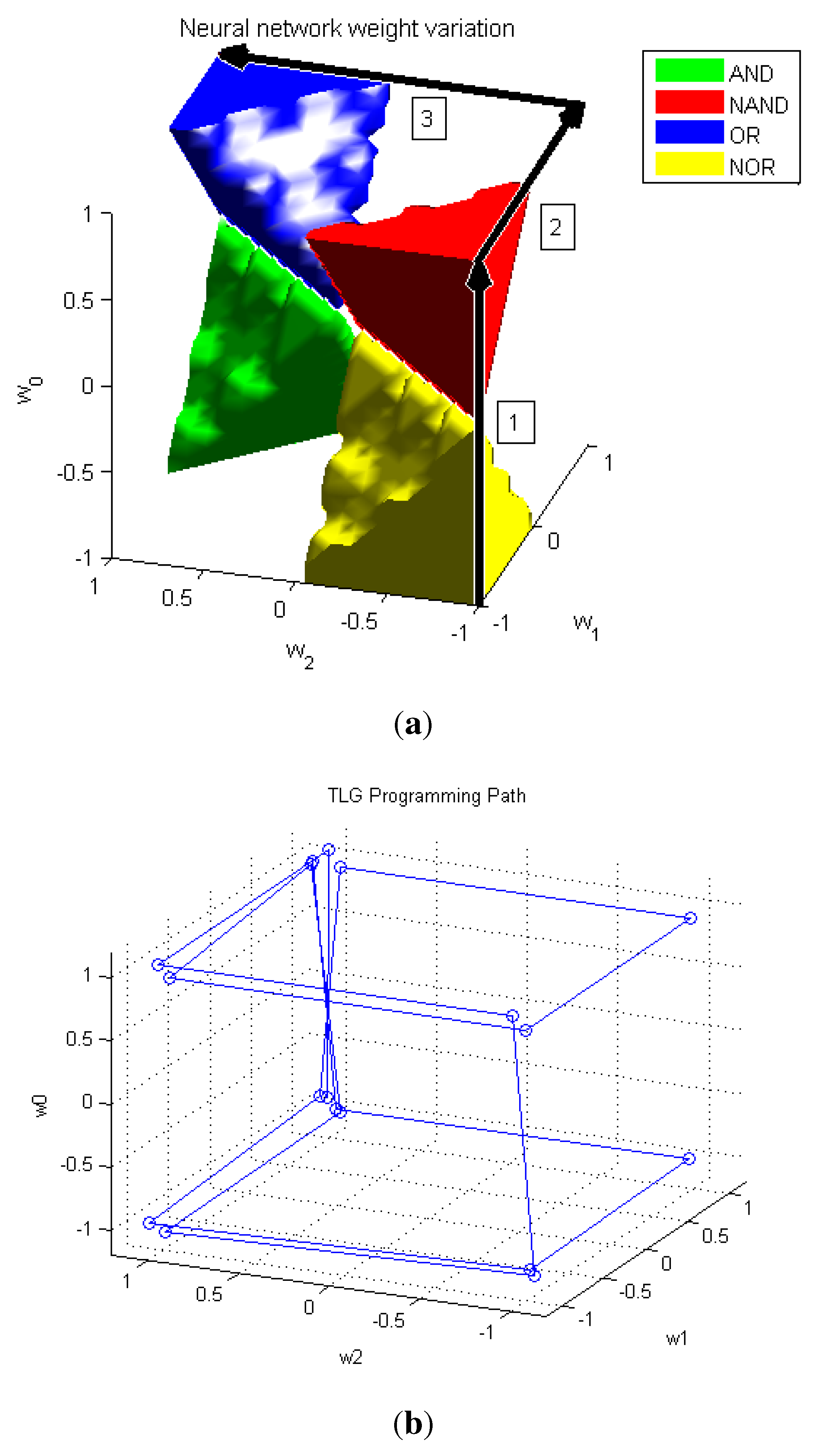
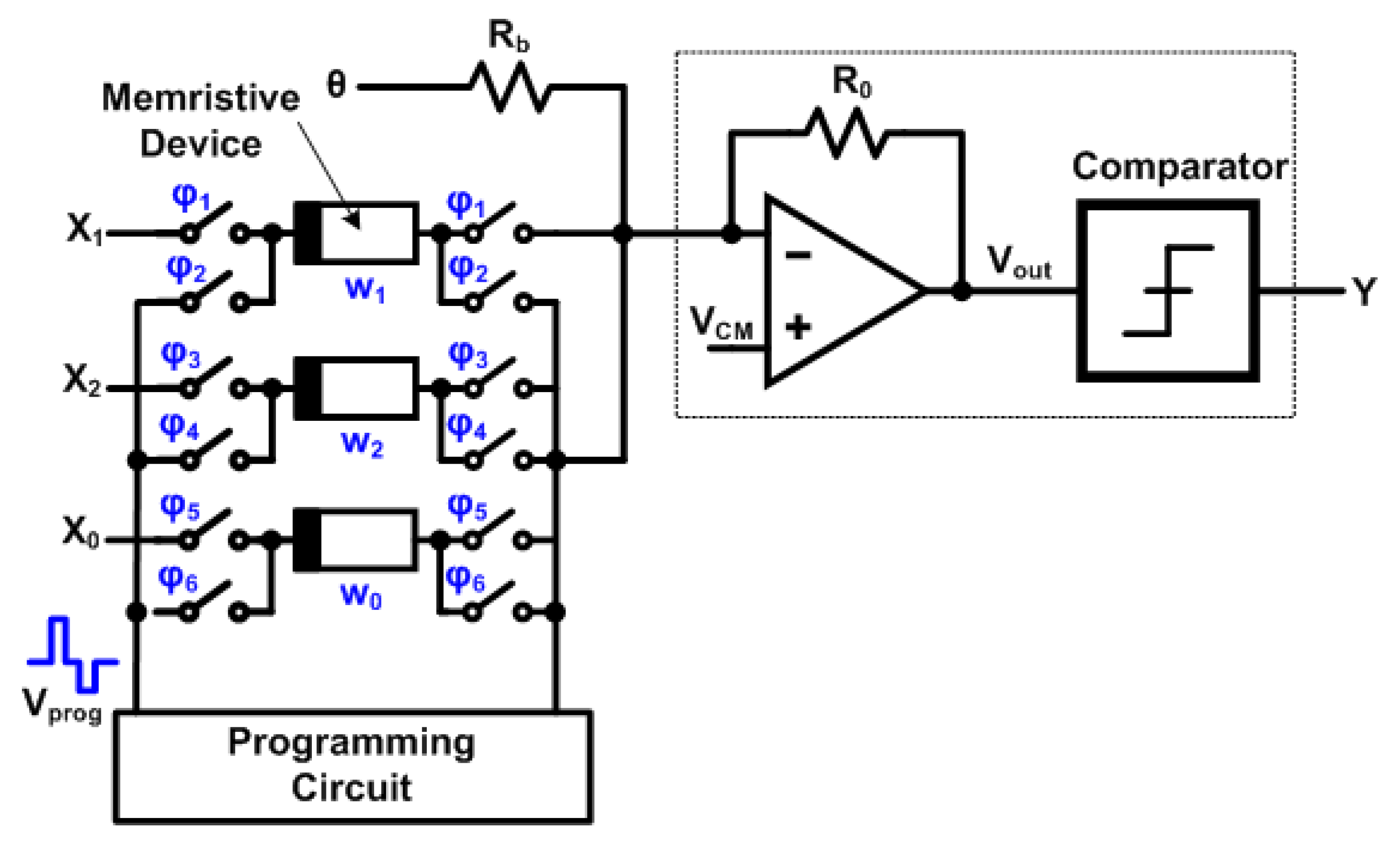
2. Threshold Logic Gate Design


| Logic operation | |||
|---|---|---|---|
| NAND | −0.5 | −0.7 | 0.5 |
| NOR | −0.5 | −0.7 | −0.5 |
| AND | 0.3 | 0.6 | −0.5 |
| OR | 0.3 | 0.6 | 0.5 |
3. Memristive Devices
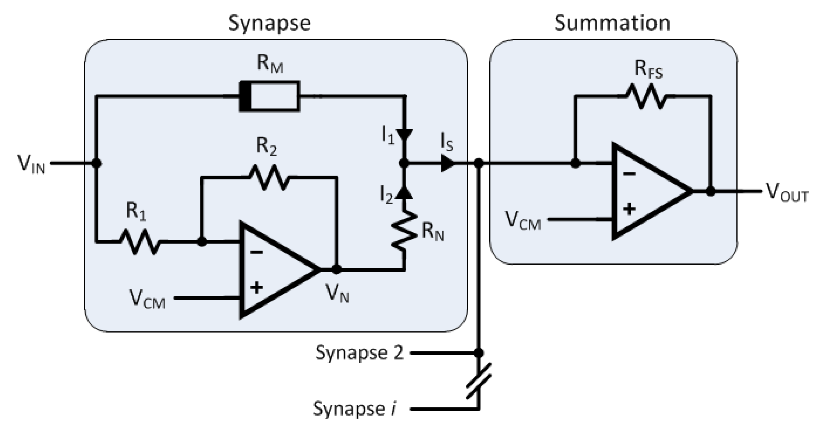
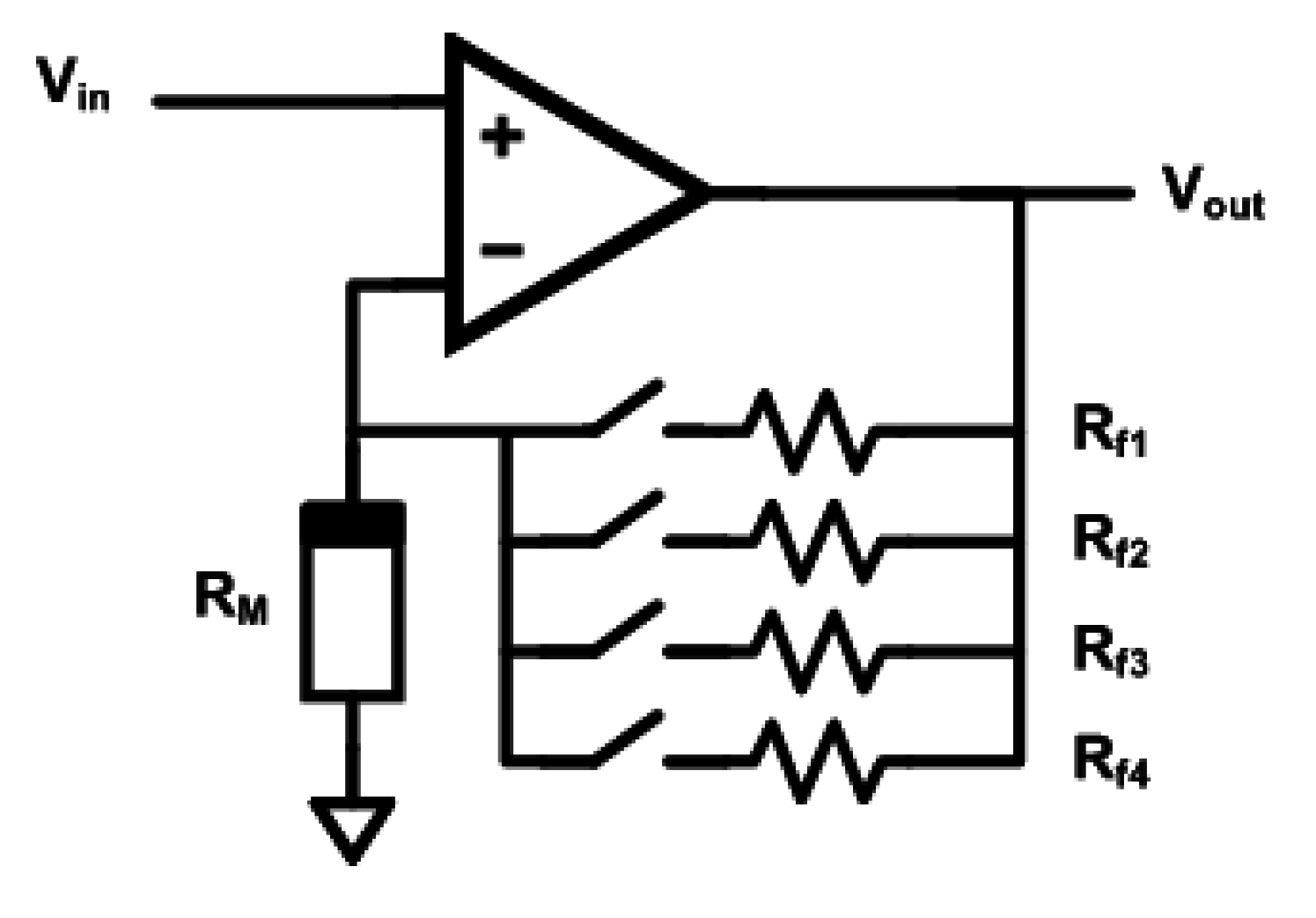
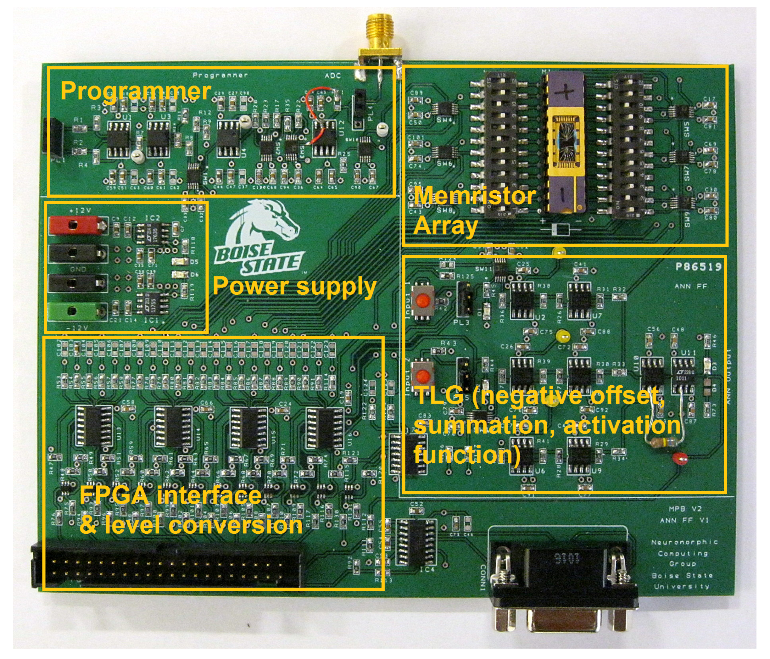
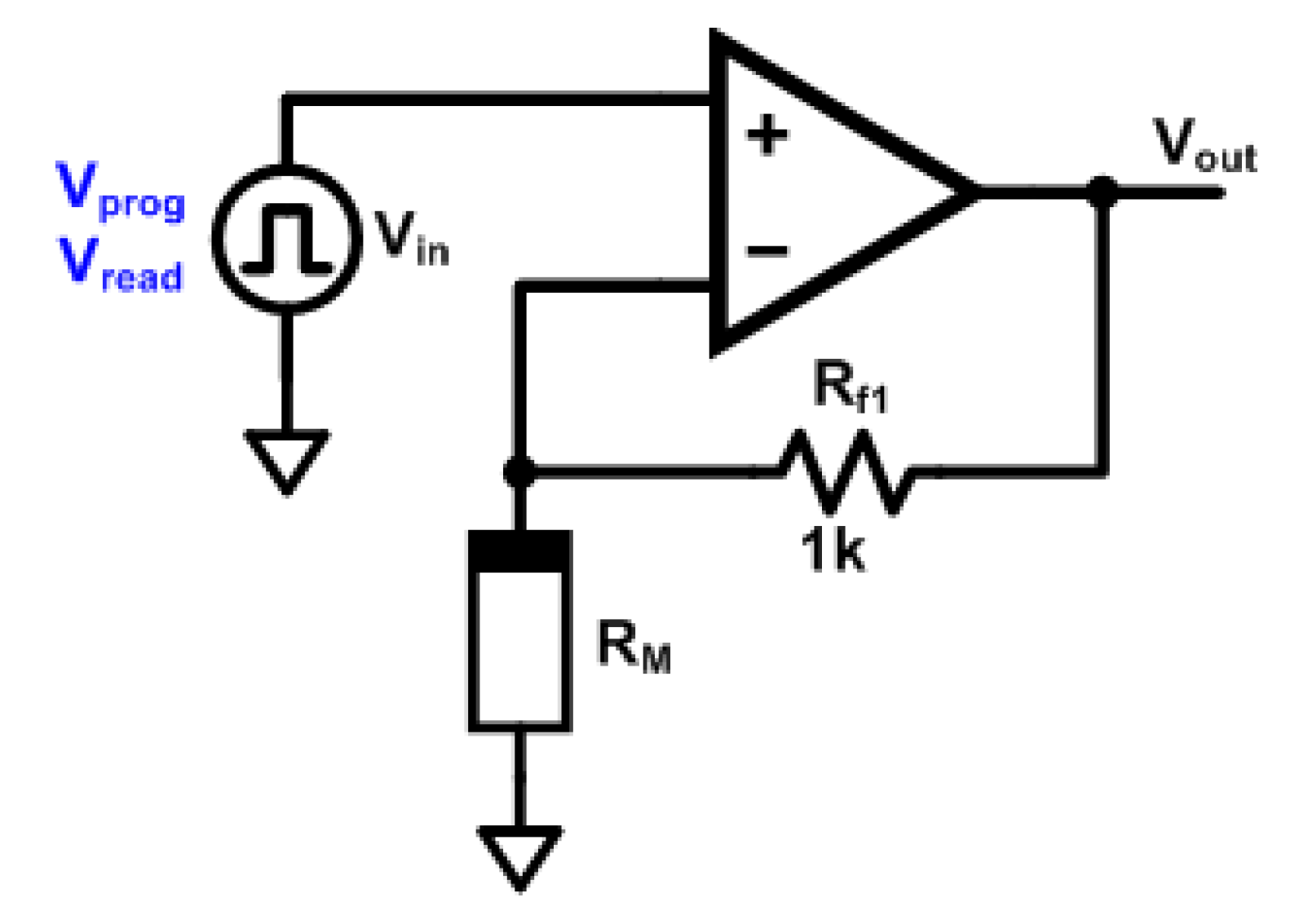
4. Circuit Realization

| Logic operation | |||
|---|---|---|---|
| NAND | 1.33 kΩ | 1.17 kΩ | 3.88 kΩ |
| NOR | 1.33 kΩ | 1.17 kΩ | 1.33 kΩ |
| AND | 2.81 kΩ | 4.81 kΩ | 1.33 kΩ |
| OR | 2.81 kΩ | 4.81 kΩ | 3.88 kΩ |
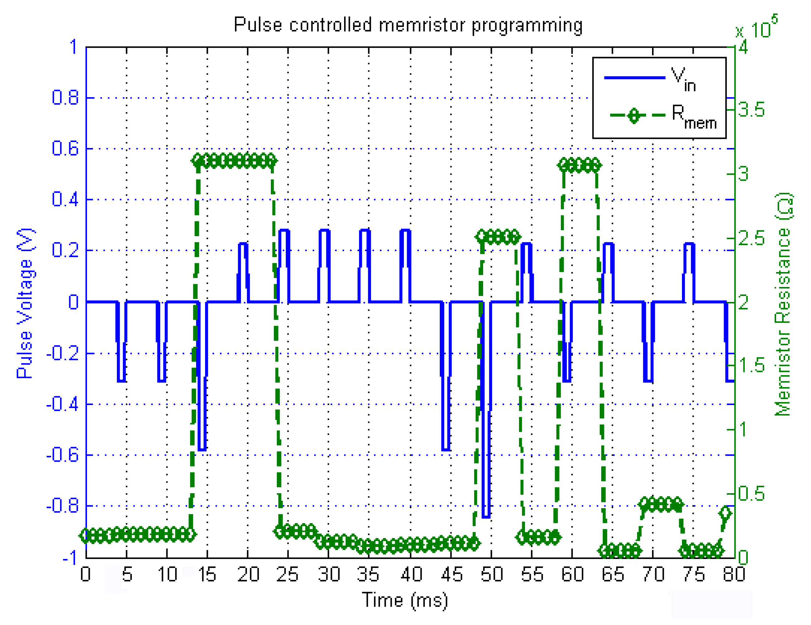
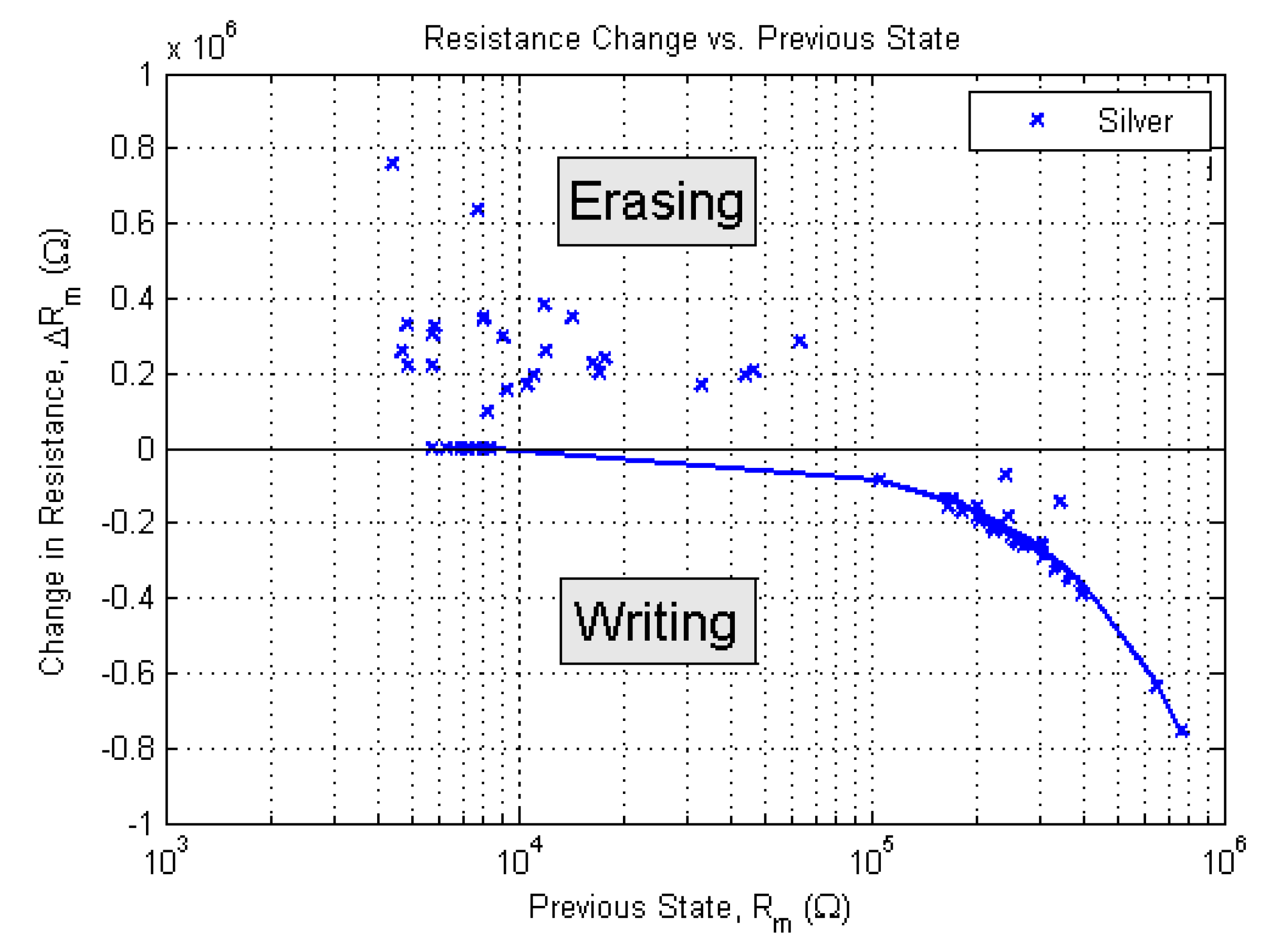
5. Memristive Device Characteristics
5.1. Simulations

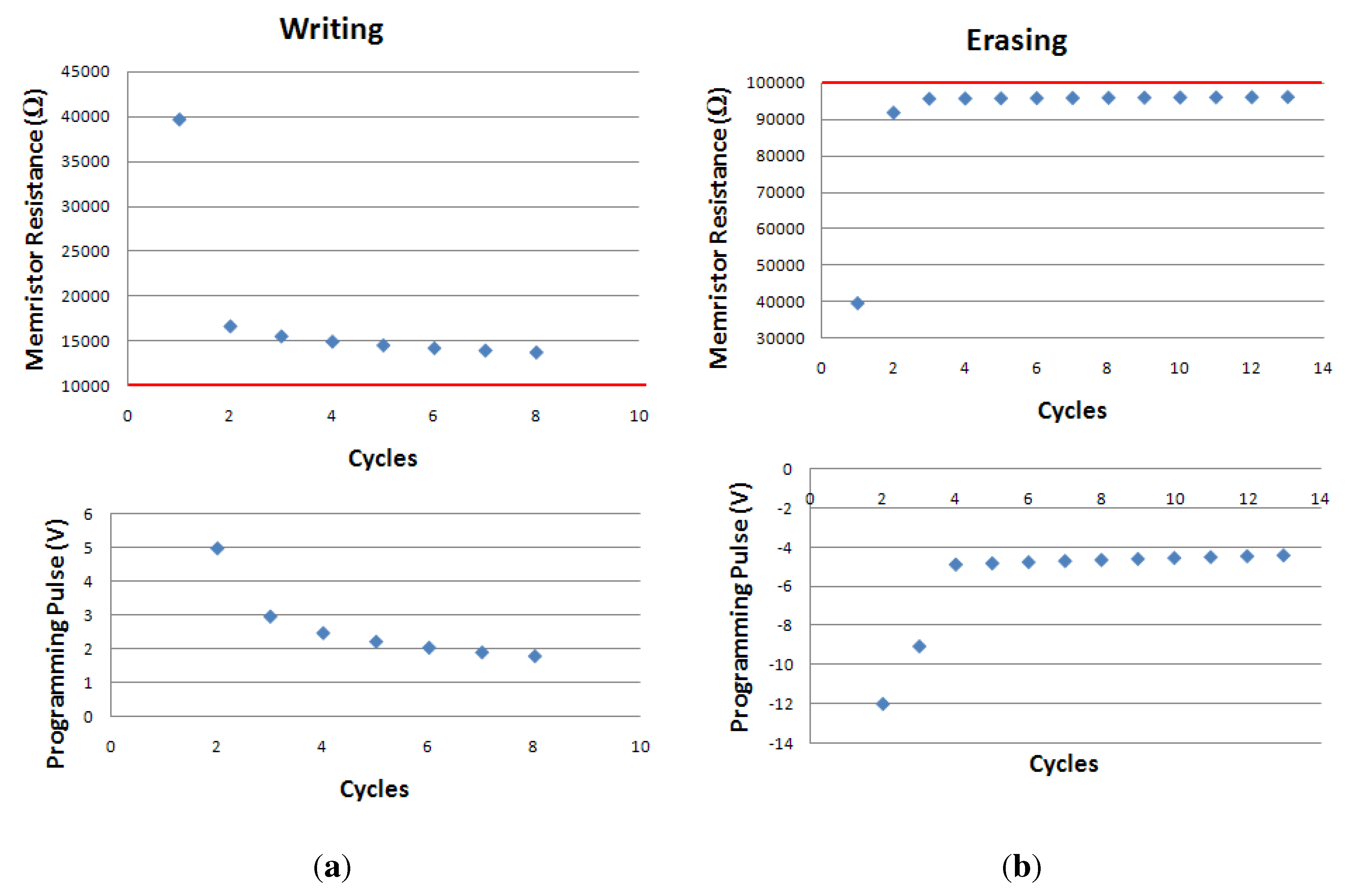
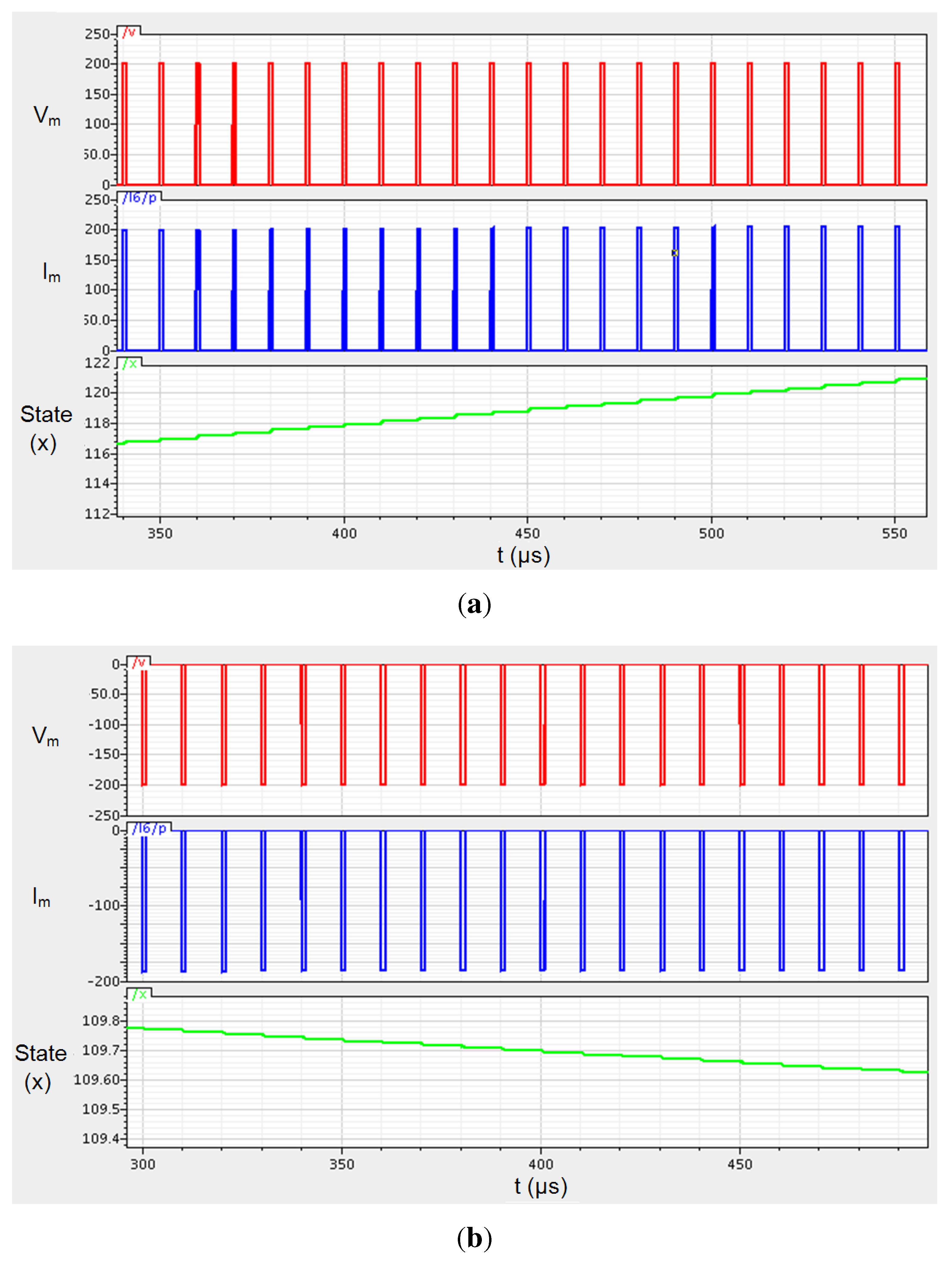
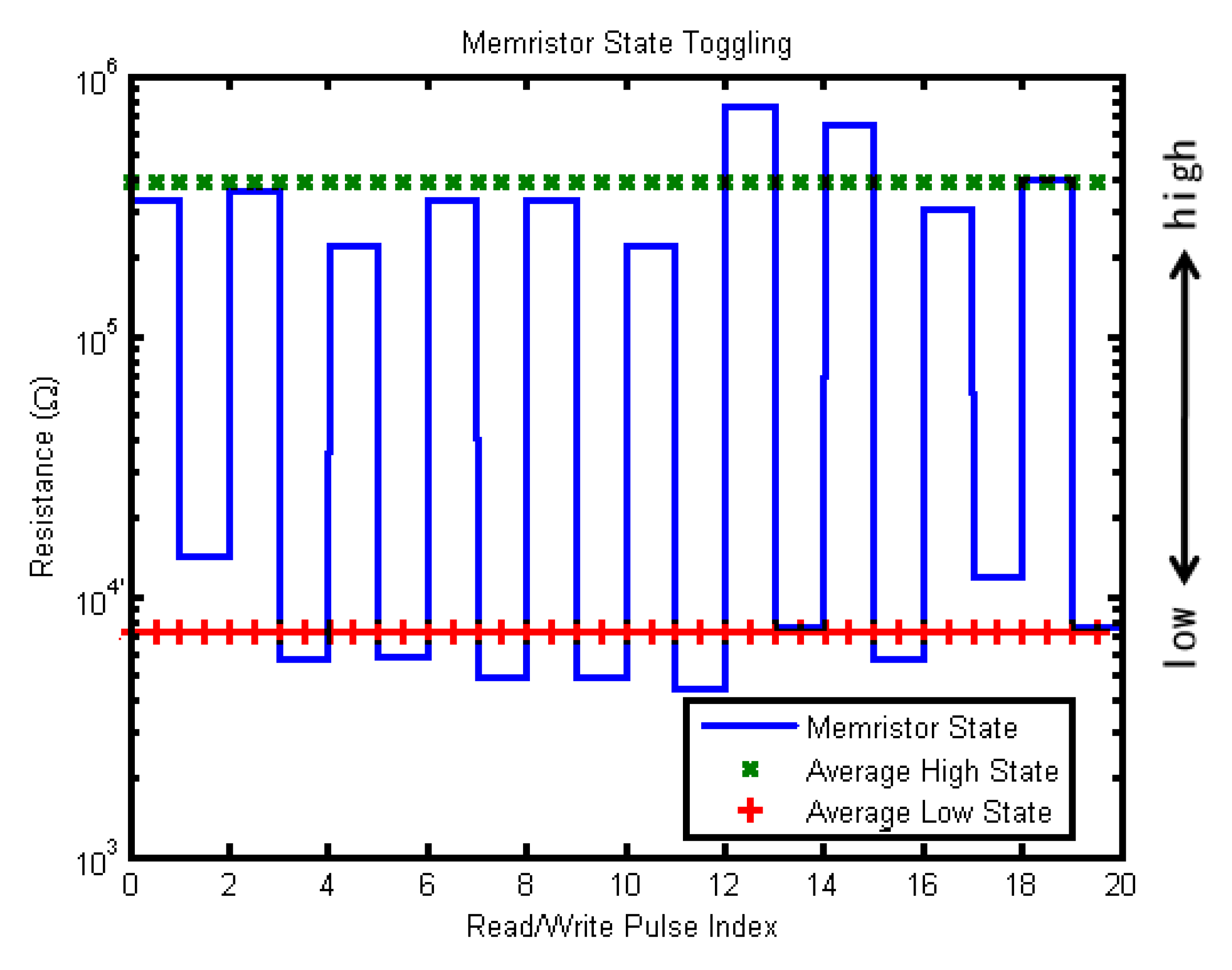
5.2. Hardware
- -
- The reading voltage should be as low as possible to prevent unintentional ion movement. For the Ag–Ch devices used for this work, the reading voltage should not exceed 40 mV.
- -
- If a large reduction in resistance has been observed after applying a writing pulse, the device should be fully erased before applying another writing pulse. A large ΔR indicates hard device switching, meaning that most of the silver from the top electrode is embedded in the amorphous insulation layer. Applying another writing pulse might irreversibly damage the device.
- -
- Erasing pulses of very short duration and high enough amplitude can cause the device to go into negative differential resistance (NDR) mode or even damage the device. Repeated mild erase pulses will not cause long-term damage.
| Programming operation | Threshold (volts) |
|---|---|
| Writing | 0.23 V |
| Erasing | −0.58 V |

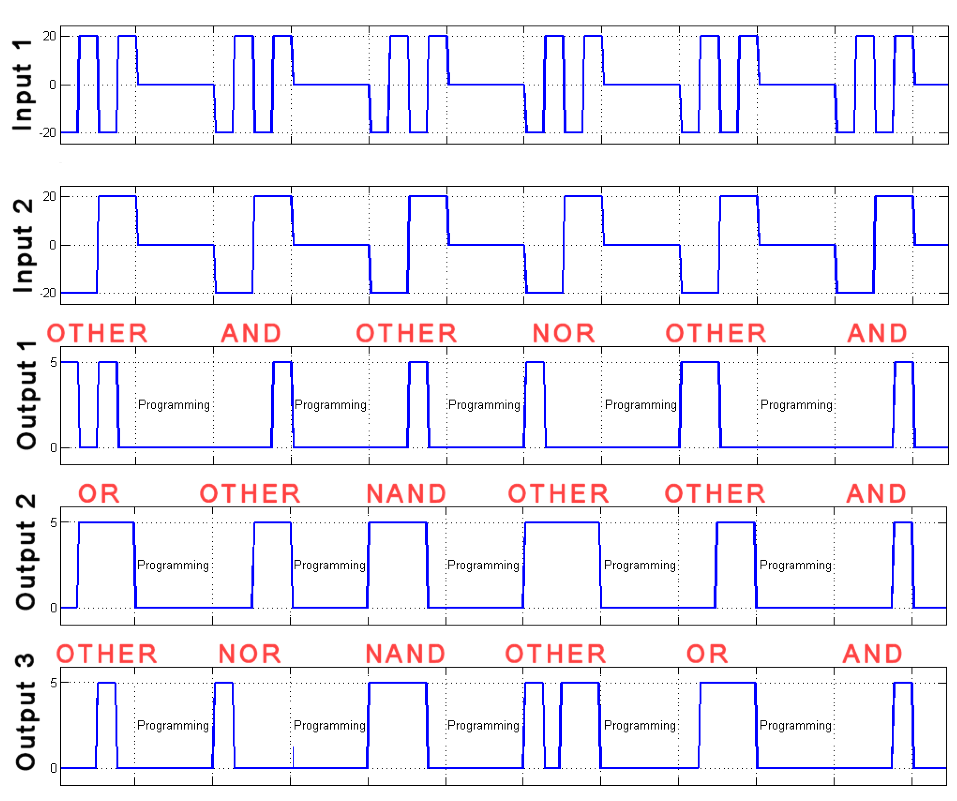
6. Experiments and Results
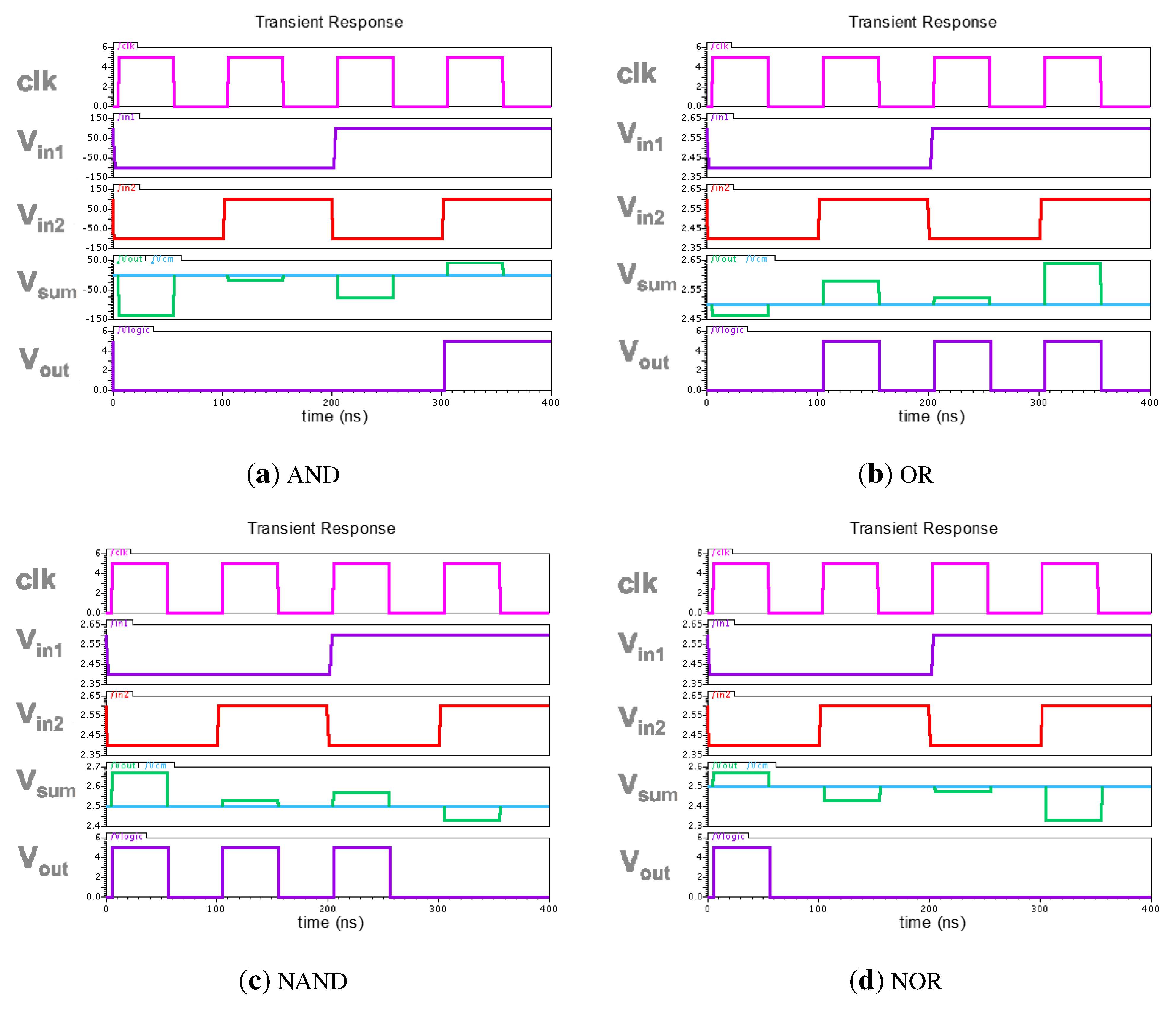
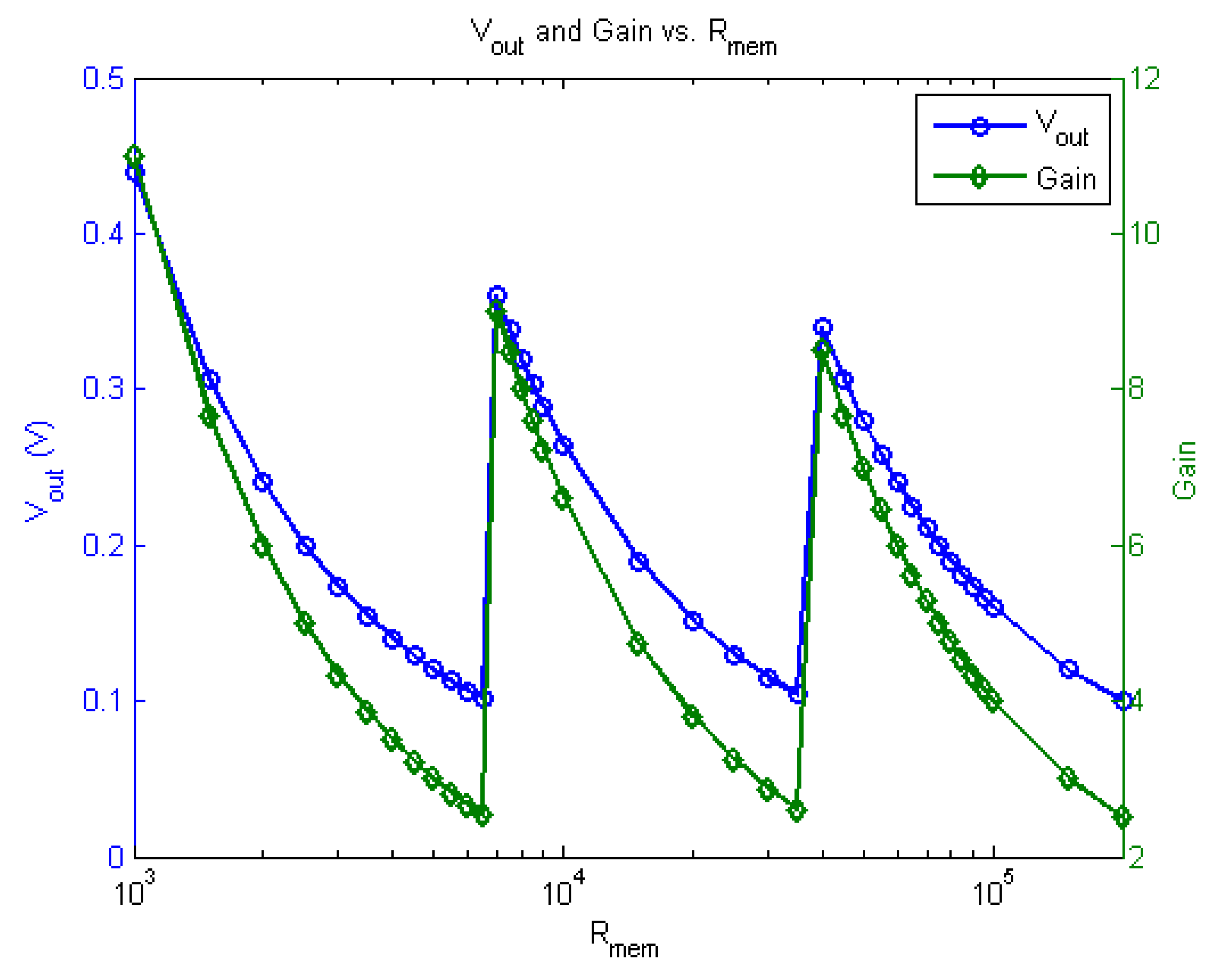
6.1. Simulations


| Logic operation | |||
|---|---|---|---|
| AND | high kΩ | high kΩ | low kΩ |
| OR | high kΩ | high kΩ | high kΩ |
| NAND | low kΩ | low kΩ | high kΩ |
| NOR | low kΩ | low kΩ | low kΩ |


7. Conclusions
Acknowledgments
References
- Strukov, D.B.; Snider, G.S.; Stewart, D.R.; Williams, R.S. The missing memristor found. Nature 2008, 453, 80–83. [Google Scholar] [PubMed]
- Strukov, D.B.; Likharev, K.K. A Reconfigurable Architecture for Hybrid CMOS/Nanodevice Circuits. In Proceedings of the 14th ACM/SIGDA International Symposium on Field Programmable Gate Arrays, Monterey, CA, USA, 22–24 February 2006; pp. 131–140.
- Beiu, V.; Quintana, J.M.; Avedillo, M.J. VLSI implementations of threshold logic—A comprehensive survey. IEEE Trans. Neural Netw. 2003, 14, 1217–1243. [Google Scholar] [CrossRef] [PubMed]
- Oblea, A.S.; Timilsina, A.; Moore, D.; Campbell, K.A. Silver Chalcogenide Based Memristor Devices. In Proceedings of the International Joint Conference on Neural Networks (IJCNN), Barcelona, Spain, 18–23 July 2010; pp. 1–3.
- Campbell, K.A. Variable integrated analog resistor. U.S. Patent No. 8238146, August 2012. [Google Scholar]
- Campbell, K.A. SnSe-based limited reprogrammable cell. U.S. Patent No. 8101936, January 2012. [Google Scholar]
- Campbell, K.A.; Moore, J.T. Silver-selenide/chalcogenide glass stack for resistance variable memory. U.S. Patent No. 8080816, December 2011. [Google Scholar]
- Campbell, K.A. Resistance variable memory device and method of fabrication. U.S. Patent No. 7868310, January 2011. [Google Scholar]
- Campbell, K.A. Differential negative resistance memory. U.S. Patent No. 7745808, June 2010. [Google Scholar]
- Campbell, K.A.; Moore, J.T. Silver-selenide/chalcogenide glass stack for resistance variable memory. U.S. Patent No. 7646007, January 2010. [Google Scholar]
- Tran, T.; Rothenbuhler, A.; Barney Smith, E.H.; Saxena, V.; Campbell, K.A. Reconfigurable Threshold Logic Gates Using Memristive Devices. In Proceedings of the IEEE Subthreshold Microelectronics Conference, Waltham, MA, USA, 9–10 October 2012.
- Merrikh-Bayat, F.; Shouraki, S.B. Memristor-based circuits for performing basic arithmetic operations. Procedia Comput. Sci. 2011, 3, 128–132. [Google Scholar] [CrossRef]
- Di Ventra, M.; Pershin, Y.V.; Chua, L.O. Circuit elements with memory: Memristors, memcapacitors, and meminductors. Proc. IEEE 2009, 97, 1717–1724. [Google Scholar] [CrossRef]
- Yuriy, P.V.; Di Ventra, M. Practical approach to programmable analog circuits with memristors. IEEE Trans. Circuits Syst. Regul. Pap. 2010, 57, 1857–1864. [Google Scholar]
- Talukdar, A.; Radwan, A.G.; Salama, K.N. Generalized model for Memristor-based Wien family oscillators. Microelectron. J. 2011, 42, 1032–1038. [Google Scholar] [CrossRef]
- Muthuswamy, B. Implementing memristor based chaotic circuits. Int. J. Bifurc. Chaos 2010, 20, 1335–1350. [Google Scholar] [CrossRef]
- Rose, G.S.; Rajendran, J.; Manem, H.; Karri, R.; Pino, R.E. Leveraging memristive systems in the construction of digital logic circuits. Proc. IEEE 2012, 100, 2033–2049. [Google Scholar] [CrossRef]
- Victor, E.; Howard, G.D.; Adamatzky, A. Organic memristor devices for logic elements with memory international. J. Bifurc. Chaos 2012, 22, 1250283. [Google Scholar] [CrossRef]
- Qiangfei, X.; Robinett, W.; Cumbie, M.W.; Banerjee, N.; Cardinali, T.J.; Yang, J.J.; Wu, W.; Li, X.; Tong, W.M.; Strukov, D.B.; Snider, G.S.; Medeiros-Ribeiro, G.; Williams, R.S. Memristor? CMOS hybrid integrated circuits for reconfigurable logic. Nano Lett. 2009, 9, 3640–3645. [Google Scholar]
- Robinett, W.; Pickett, M.; Borghetti, J.; Qiangfei, X.; Snider, G.S.; Medeiros-Ribeiro, G.; Williams, R.S. A memristor-based nonvolatile latch circuit. Nanotechnology 2010, 21. [Google Scholar] [CrossRef] [PubMed]
- Snider, G.S. Self-organized computation with unreliable, memristive nanodevices. Nanotechnology 2007, 18, 1–13. [Google Scholar] [CrossRef]
- Adhikari, S.P.; Yang, C.; Kim, H.; Chua, L.O. Memristor bridge synapse-based neural network and its learning. IEEE Trans. Neural Netw. Learn. Syst. 2012, 23, 1426–1435. [Google Scholar] [CrossRef] [PubMed]
- Ziegler, M.; Soni, R.; Patelczyk, T.; Ignatov, M.; Bartsch, T.; Meuffels, P.; Kohlstedt, H. An electronic version of Pavlov’s dog. Adv. Funct. Mater. 2012, 22, 2744–2749. [Google Scholar] [CrossRef]
- Bichler, O.; Zhao, W.; Alibart, F.; Pleutin, S.; Lenfant, S.; Vuillaume, D.; Gamrat, C. Pavlov’s dog associative learning demonstrated on synaptic-like organic transistors. Neural Comput. 2013, 25, 549–566. [Google Scholar] [CrossRef] [PubMed]
- Yu, S.; Wu, Y.; Jeyasingh, R.; Kuzum, D.; Wong, H.-S.P. An electronic synapse device based on metal oxide resistive switching memory for neuromorphic computation. IEEE Trans. Electron Devices 2011, 58, 2729–2737. [Google Scholar] [CrossRef]
- Jo, S.H.; Chang, T.; Ebong, I.; Bhadviya, B.B.; Mazumder, P.; Lu, W. Nanoscale memristor device as synapse in neuromorphic systems. Nano Lett. 2010, 10, 1297–1301. [Google Scholar] [CrossRef] [PubMed]
- Pino, R.; Bohl, J.W.; McDonald, N.; Wysocki, B.; Rozwood, P.; Campbell, K.A.; Oblea, A.; Timilsina, A. Compact Method for Modeling and Simulation of Memristor Devices: Ion Conductor Chalcogenide Based Memristor Devices. In Proceedings of the 2010 IEEE/ACM International Symposium on Nanoscale Architectures (NANOARCH), Anaheim, CA, USA, 17–18 June 2010; pp. 1–4.
- Yakopcic, C.; Taha, T.M.; Subramanyam, G.; Pino, R.E.; Rogers, S. A memristor device model. IEEE Electron Device 2011, 32, 1436–1438. [Google Scholar] [CrossRef]
- Yakopcic, C.; Taha, T.M.; Subramanyam, G.; Shin, E.; Murray, P.T.; Rogers, S. Memristor-basedPattern Recognition for Image Processing: An Adaptive Coded Aperture Imaging and Sensing Opportunity. In Proceedings of the Adaptive Coded Aperture Imaging, Non-Imaging, and Unconventional Imaging Sensor Systems II, San Diego, CA, USA, 1 August 2010; Volume 7818, p. 78180E.
- Yakopcic, C.; Sarangan, A.; Gao, J.; Taha, T.M.; Subramanyam, G.; Rogers, S. TiO2 Memristor Devices. In Proceedings of the 2011 IEEE National Aerospace and Electronics Conference (NAECON), Dayton, OH, USA, 20–22 July 2011; pp. 101–104.
- Yakopcic, C.; Taha, T.M.; Subramanyam, G.; Pino, R.E.; Rogers, S. Analysis of a Memristor Based 1T1M Crossbar Architecture. In Proceedings of the 2011 International Joint Conference on Neural Networks (IJCNN), San Jose, CA, USA, 31 July–5 August 2011; pp. 3243–3247.
- Yakopcic, C.; Taha, T.M.; Subramanyam, G.; Rogers, S. Memristor-based unit cell for a detector readout circuit. SPIE Optical Eng. Appl. 2011, 8165, 81651F. [Google Scholar]
- Yakopcic, C.; Taha, T.M.; Subramanyam, G.; Pino, R.E. Memristor SPICE modeling. In Advances in Neuromorphic Memristor Science and Applications; Springer: Berlin, Germany, 2012; pp. 212–244. [Google Scholar]
- Drake, K.; Campbell, K.A. Chalcogenide-Based Memristive Device Control of a Lego Mindstorms NXT Servo Motor. In Proceedings of the AIAA Infotech at Aerospace Conference and Exhibit, St. Louis, MO, USA, 29–31 March 2011.
- Jo, S.H.; Kim, K.-H.; Lu, W. Programmable resistance switching in nanoscale two-terminal devices. Nano Lett. 2008, 9, 496–500. [Google Scholar] [CrossRef] [PubMed]
- Zamarreño-Ramos, C.; Camuñas-Mesa, L.A.; Pérez-Carrasco, J.A.; Masquelier, T.; Serrano-Gotarredona, T.; Linares-Barranco, B. On spike-timing-dependent-plasticity, memristive devices, and building a self-learning visual cortex. Front. Neurosci. 2011, 5(26). [Google Scholar] [CrossRef] [PubMed]
© 2013 by the authors; licensee MDPI, Basel, Switzerland. This article is an open access article distributed under the terms and conditions of the Creative Commons Attribution license (http://creativecommons.org/licenses/by/3.0/).
Share and Cite
Rothenbuhler, A.; Tran, T.; Smith, E.H.B.; Saxena, V.; Campbell, K.A. Reconfigurable Threshold Logic Gates using Memristive Devices. J. Low Power Electron. Appl. 2013, 3, 174-193. https://doi.org/10.3390/jlpea3020174
Rothenbuhler A, Tran T, Smith EHB, Saxena V, Campbell KA. Reconfigurable Threshold Logic Gates using Memristive Devices. Journal of Low Power Electronics and Applications. 2013; 3(2):174-193. https://doi.org/10.3390/jlpea3020174
Chicago/Turabian StyleRothenbuhler, Adrian, Thanh Tran, Elisa H. Barney Smith, Vishal Saxena, and Kristy A. Campbell. 2013. "Reconfigurable Threshold Logic Gates using Memristive Devices" Journal of Low Power Electronics and Applications 3, no. 2: 174-193. https://doi.org/10.3390/jlpea3020174