1. Introduction
In recent years, there has been an increasing interest in the application of portable battery powered biomedical devices in consumer products. To increase the operation time of the battery employed in biomedical products, the system needs to be designed for low-voltage and low-power consumption. Several biomedical applications like electro-cardiogram (ECG), electroencephalogram (EEG), and evoked potential (EP) employ digital signal processing (DSP) techniques after digitizing the sensed analog signals. The analog-to-digital data converter (ADC), used for digitizing the sensed analog signal, is a critical and power hungry block in a generic biomedical system [
1].
The ADC employed in biomedical signal processing chain typically requires 1–6 kHz signal bandwidth with up to 14-bits or higher resolution [
1]. Delta-sigma modulation based ADCs employing an oversampling technique are a well-known candidate for achieving higher resolution analog-to-digital conversion using a low-resolution quantizer [
2,
3,
4,
5]. Using oversampling techniques, the quantization noise introduced by the low-resolution quantizer is pushed outside the signal bandwidth, which results in higher resolution (SNR) and dynamic range (DR). Also, ΔΣ ADCs are well-suited for digitizing biomedical signals without requiring any instrumentation amplifier. When compared to other conventional ADCs, small differential-mode signal can be recovered with high resolution using a ΔΣ modulator [
2,
3,
4,
5].
The ΔΣ ADC is also proven to be well suitable for low-bandwidth signal conversion by employing oversampling, and is robust to device mismatches in the forward signal path when using nano-CMOS processes [
5,
6,
7]. Traditionally, discrete-time (DT) ΔΣ ADC were the commonly used ΔΣ architecture. Many such modulators have been reported over previous decades [
8,
9]. However, in recent years, the continuous-time delta-sigma (CT-ΔΣ) ADC is being preferred in low-power signal-processing applications due to several attractive features like an inherent anti-aliasing filter (AAF), relaxed bandwidth requirements of the active elements and lower power consumption when compared to their discrete-time counterparts [
3,
5,
7].
To enhance the power reduction in battery-powered, low-bandwidth biomedical applications, a single-bit CT-ΔΣ ADC is an appropriate choice. Advantages of using a single-bit quantizer include reduced chip area and significant power reduction of the ΔΣ loop. However, some important concerns in designing single-bit CT-ΔΣ include the higher in-band quantization noise due to the use of a single-bit quantizer, increased sensitivity to clock jitter and the slew rate requirement for the first operational amplifier (opamp). The higher in-band quantization noise can be addressed by increasing the effective oversampling ratio (OSR). Since the signal bandwidth requirement of battery powered biomedical applications is low, even with lower sampling rate a higher OSR can be employed. Also, due to the low sampling frequencies used in the CT-ΔΣ ADCs for biomedical applications, clock jitter is not a serious concern.
Any amount of slewing in the opamp introduces distortion and increases the in-band noise, resulting in a reduction of signal to quantization noise (SQNR) [
10]. This should be taken care of by careful design of the opamp. The main bottleneck in achieving low-power CT-ΔΣ ADC design is the power requirement of the loop-filter integrators. Any power reduction in opamp reduces the finite DC gain and unity-gain frequency (
fun) of the opamp. The lower
fun of opamp impairs the characteristics of the loop-filter and thus modifies the modulator noise transfer function (NTF) with significant performance degradation. In order to achieve a low-power design with acceptable performance, the systematic design centering method proposed in [
11] is adopted in this work. Further, the use of a subthreshold optimized FDSOI CMOS process in this design resulted in a low-power circuit-level implementation.
This invited paper presents an expanded and detailed discussion on our previous work reported in [
5]. The remainder of this paper is organized as follows.
Section 2 illustrates the modulator architecture for this application.
Section 3 demonstrates the design of the third-order modulator using systematic design centering to overcome the opamp non-idealities.
Section 4 briefly explains the design of the CT-ΔΣ blocks.
Section 5 discusses the simulation results of the designed third-order low power CT-ΔΣ. Finally,
Section 6 draws conclusions about the work.
2. Choice of Architecture
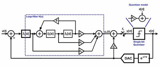
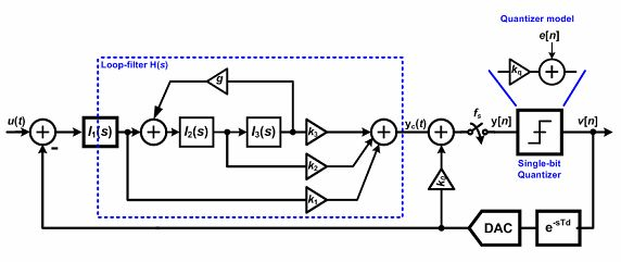
Figure 1 shows the generalized single-ended equivalent block diagram of a single-loop CT-ΔΣ modulator. The ΔΣ ADC consists of an analog modulator followed by a digital decimation filter. In this figure,
L(
s) is the continuous-time loop filter whose output is sampled and quantized at using a quantizer operating at a sampling rate,
fs, equivalent time period (
Ts). The quantizer can either be a single-bit (a comparator) or a multi-bit implementation using a Flash ADC. The modulator employs an oversampling ratio denoted by OSR and the quantizer has an excess-delay of
Td, which is modeled as e
−sTd in
Figure 1. Here,
u(
t) is the modulator input signal, y
c(
t) and y[
n] are the continuous-time and sampled loop-filter outputs respectively, v[
n] is the digital output of the modulator,
Dout[
n] is the decimated digital output of the ADC with a clock-rate of
fs/OSR. In this section, we describe the various architectural choices made in our CT-ΔΣ modulator design.
Figure 1.
A generalized single-ended block diagram of a Continuous-time ΔΣ Modulator.
Figure 1.
A generalized single-ended block diagram of a Continuous-time ΔΣ Modulator.
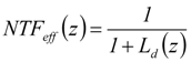
2.1. Choice of Noise-Transfer Function NTF(z)
The choice of proper noise transfer function,
NTF(z), plays a prominent role in the modulator performance. In a single-bit CT-ΔΣ modulator design, increasing the order of the NTF may lead to instability and also reduce the maximum stable amplitude (MSA) for the input signal, which degrades the dynamic range of the ADC [
1,
4,
5]. Thus, to achieve a SNR higher than 90 dB for the desired signal bandwidth with reasonable layout area, a third-order NTF with oversampling ratio of 512 is chosen. As it will be evident later, the large OSR value was chosen to avoid excessively large layout areas for the resistances and capacitances in the loop-filter. Further, for better stability of the third-order single-bit single-loop modulator, the out-of-band gain (OBG) is limited to 1.5 [
12]. Also, complex zeros are placed in the signal band to improve the noise shaping performance [
1,
4,
5]. For a stable single-bit CT-ΔΣ modulator design, it is essential to account for the effective quantizer gain (
kq) as depicted in
Figure 2. The effective gain of the single-bit quantizer is estimated by curve fitting the behavioral simulation results and is given by
![Jlpea 02 00197 i001]()
, where
E[
x] is the estimation operator on the discrete-time sequence
x[
n] [
4]. Thus, an effective
NTF1(
z) is obtained by substituting a suitable value of
kq.
Figure 3 shows the magnitude response of the modulator NTF fitted to the modulator’s response using the effective quantizer gain
kq.
2.2. Choice of Loop Filter Architecture
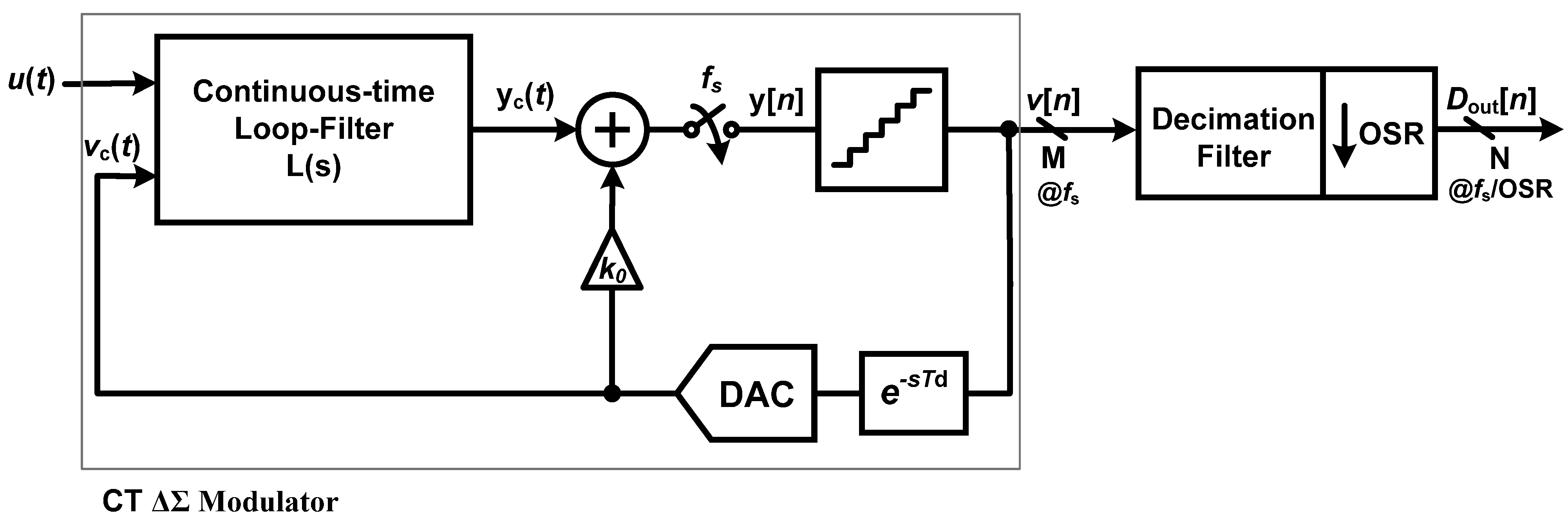
A cascade of integrators with a distributed feedforward summation architecture is used to implement the third-order loop filter of the single-bit CT-ΔΣ.
Figure 2 shows the simple block diagram of CIFF modulator architecture.
Figure 2.
Block diagram of the CIFF modulator architecture.
Figure 2.
Block diagram of the CIFF modulator architecture.
The principle advantage of feedforward architecture is that the input signal content in the successive integrator outputs is progressively scaled down from the first integrator to the last integrator in the loop-filter, and thus the loop-filter output is largely composed of the shaped quantization noise. This can be used to our benefit by scaling down the integrator performance requirements from the first to the last integrator resulting in an overall reduction in modulator power consumption. An active-RC topology is chosen for the loop filter because of its high linearity and low noise characteristics [
3,
5,
7,
10]. Since the first integrator sets the input referred noise and distortion for the overall modulator, the performance requirements from the first opamp are higher than the rest of the opamps [
10,
13].
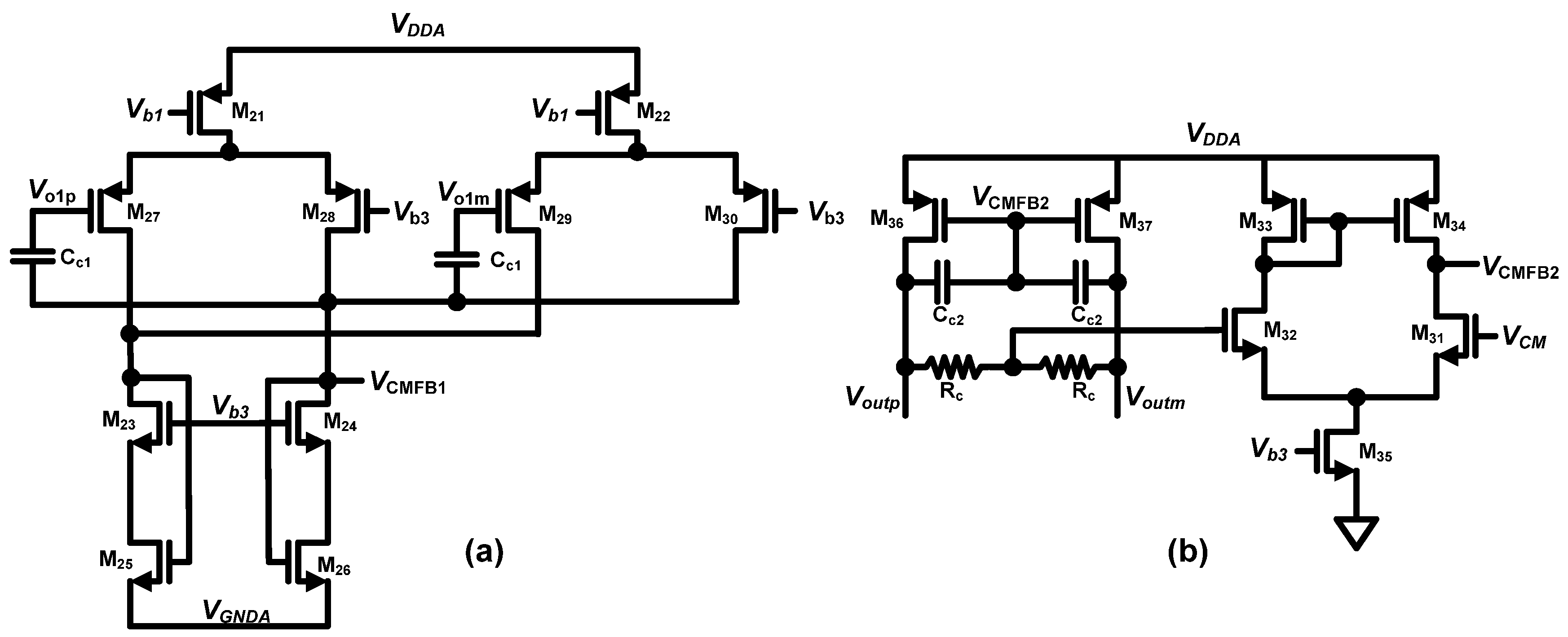
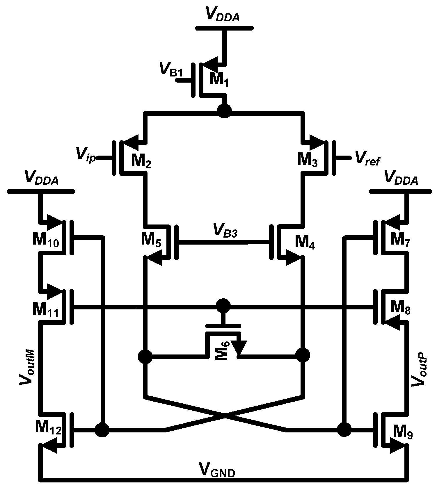
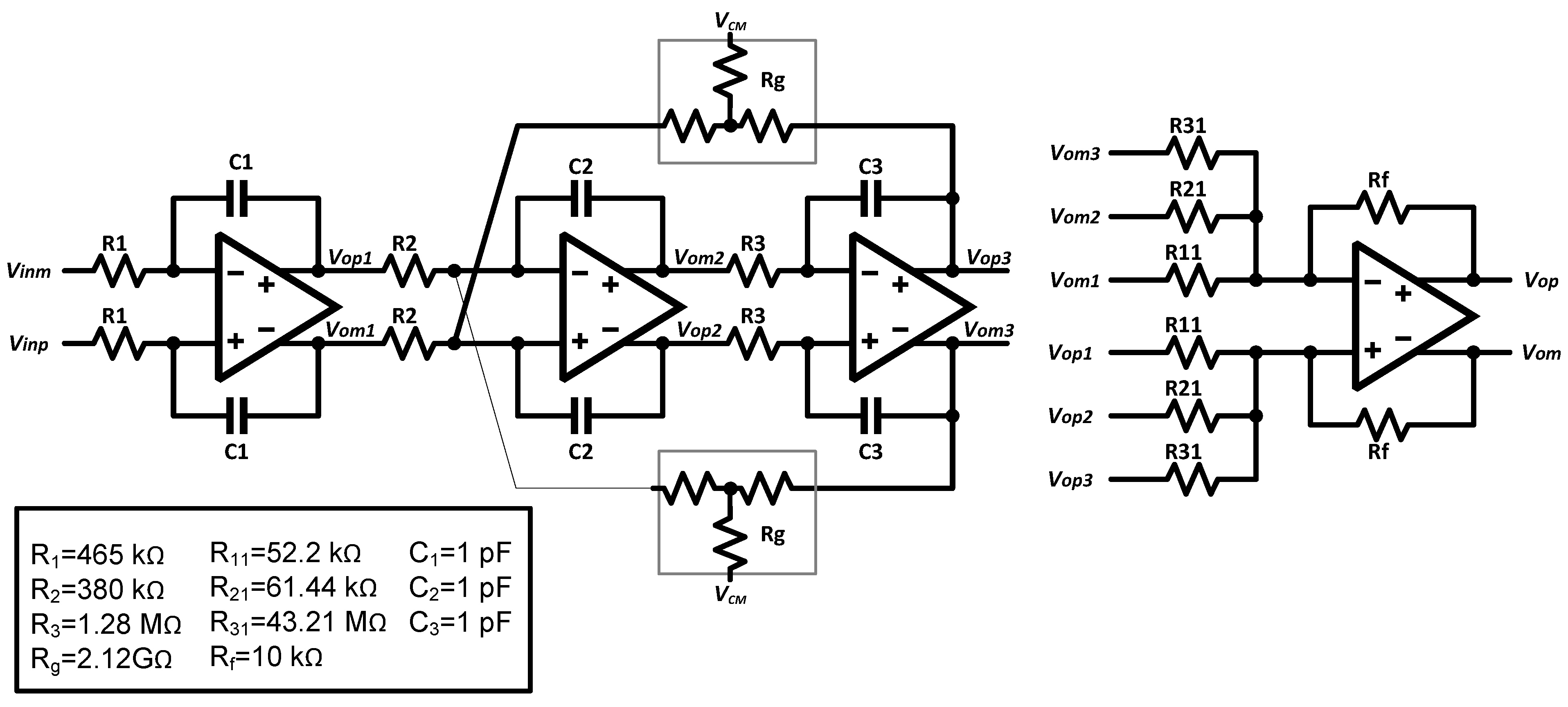
Figure 4 shows the circuit-level schematic of the third-order CT-ΔΣ loop-filter along with the resistance and capacitance values used in the design. The integrators
I1(s),
I2(s), and
I3(s) in
Figure 3 are realized using opamps
A1,
A2 and
A3 respectively, as shown in
Figure 4. The summing node before the sampler is implemented using opamp
A4. The feedforward coefficients
K( = [
k0 k1 k2 k3]) and summation are implemented using resistors (
R11,
R21,
R31,
Rf) and a summing amplifier (
A4). Since the RC time-constants in the loop-filter are inversely proportional to the sampling frequency (
fs), a lower sampling frequency (and thus lower OSR value) would have resulted in either very large values for resistors (1–10 MΩ range) or capacitor values of 10 pF range. Large values for resistances would result in larger layout area and higher distributed parasitic capacitance. On the other hand, large capacitance loads would result in higher power consumption in the opamps driving them. This provides justification for our selected OSR value of 512.
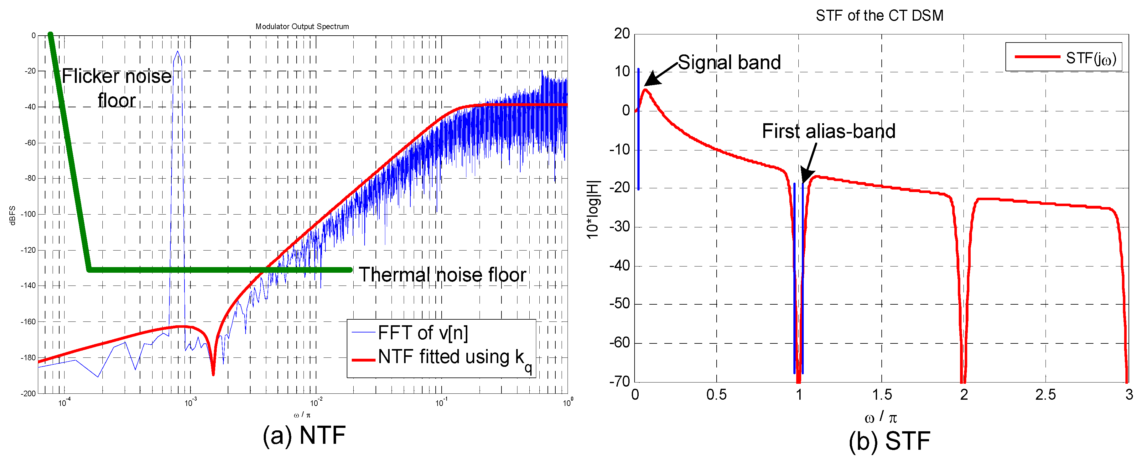
Figure 3(a) illustrates the ideal noise shaping behavior of the CT-ΔΣ modulator seen in
Figure 2. Here, we can see that the total noise in the signal band (π/2∙OSR) is dominated by the thermal and flicker noise floor.
Figure 3(b) illustrates the signal transfer function, STF(jω), of the feedforward modulator. Here, the alias suppression in the first alias-band is greater than 90 dB, thanks to the input filtering provided by the CT loop-filter.
Figure 3.
Ideal NTF and STF magnitude response of the CT-ΔΣ modulator.
Figure 3.
Ideal NTF and STF magnitude response of the CT-ΔΣ modulator.
Figure 4.
Circuit-level schematic of the feedforward loop-filter with circuit parameter values.
Figure 4.
Circuit-level schematic of the feedforward loop-filter with circuit parameter values.
2.3. Thermal Noise Budget
The input referred noise of the modulator comprises of the thermal noise from the input resistor (
R1) and the input noise of the first opamp and the feedback DAC. These noise sources dominate the overall modulator in-band noise and thus the achievable SNR. The input referred noise of the opamp is dictated by the transconductance (
gm1) of the first stage diff-pair. In general, the values of
R1 and
gm1 are chosen such that each of the noise sources roughly contribute equal amount of thermal noise. Also, a PMOS differential pair with large device area is used in the first-stage of the first opamp to subside the effect of the flicker noise on the overall modulator SNR. The value of these circuit design variables (
R1,
gm1, sizing of the feedback resistive DAC) have been chosen so as to keep the total thermal noise contribution to be roughly equal to 75% of the total in-band noise. This noise budgeting approach provides sufficient noise in the modulator to dither the signal input at the quantizer and help reduce spurious tones in the single-bit modulator [
4].
2.4. Clock Jitter, Excess-Loop Delay and RC Variation
Clock jitter, excess loop delay (ELD) and RC time-constant variation are other important design concerns in a CT-ΔΣ [
14]. However, due to low sampling frequency and negligible comparator delay of 100 ps, performance degradation due to the excess loop delay is insignificant in the present design. Also, due to the low sampling frequency required, clock jitter is not expected to degrade the modulator performance [
15]. Finally, to mitigate the effect of systematic RC time-constant variation (±30%) due to process shift, a tuning method using a digitally programmable capacitor bank can be implemented [
7].
3. Loop-Filter Design Using Systematic Design Centering
Using high-level modeling methods and tools, a loop-filter transfer function is designed using active-RC integrators. Initial modeling uses behavioral models of opamps with suitable parameters for DC gain, unity-gain bandwidth and linearity, and corresponding component values are derived for desired SNDR and dynamic range. After appropriate architecture selection of the opamps, the behavioral opamps are replaced by their transistor-level schematics.
Conventionally, the third-order loop-filter coefficients
K= [
k0 k1 k2 k3], are obtained by fitting the impulse response of the discrete-time loop filter
Ld(
z)
= 1
− NTF−1(
z) to the continuous-time loop-filter,
Lc(
s), using the impulse invariance transformation (IIT) for a given feedback DAC pulse shape [
14]. The assumption in this method is that the integrators are ideal, with a transfer function given by
![Jlpea 02 00197 i002]()
. This impulse response fitting method breaks down when applied to real integrators with finite op-amp DC gain, non-dominant opamp poles and the presence of opamp zeros. To get the desired
NTFeff(
z), either the filter coefficients (
K) need to be further tuned or the DC gain and the unity-gain frequency (
fun) of the opamp must be sufficiently large. The latter will result in an increase in the modulator power consumption [
11,
16]. Also, in a single-bit single-loop CT-ΔΣ modulator, more than 90% of the power is consumed by the opamp, which is a key design block in the loop-filter. In order to achieve low power consumption in the modulator, the bias currents in the opamps need to be optimized for the given specification. Any power reduction in the opamp impairs the characteristics of the loop-filter and thus impacts the resulting NTF performance.
Figure 5 shows the magnitude response of
NTF(
z) with ideal and real integrators for the same loop-filter. It can be seen that the systematic design method restores the modulator NTF with integrators implemented using real opamps having two poles and a zero. Moreover, it is also essential that the slewing in the opamps is sufficiently limited so as not to degrade the overall modulator linearity.
Figure 5.
Magnitude responses of the resulting NTF with real integrators, with and without systematic design centering.
Figure 5.
Magnitude responses of the resulting NTF with real integrators, with and without systematic design centering.
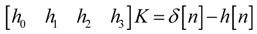
A systematic design centering method for obtaining the loop-filter coefficients by including the effect of the integrator non-idealities is employed [
11]. We briefly describe this method for third-order CT-ΔΣ as follows: as we know, the relationship between the noise-transfer function,
NTF(
z), and the discrete-time loop-filter response,
Ld(
z), is given
This relation (Equation 1) is incorporated into the impulse response fitting by using the following relation [
5]
where
h[
n] is the impulse response of the
NTF(
z). Further
![Jlpea 02 00197 i005]()
, where
![Jlpea 02 00197 i006]()
and
![Jlpea 02 00197 i007]()
represent the sampled DAC pulse response of direct path and at the output
ith integrator (see [
11] for details).
Table 1 shows the derived loop-filter coefficients for the modulator, before and after systematic design procedure.
Table 1.
Loop-filter coefficients for the modulator.
Table 1.
Loop-filter coefficients for the modulator.
| k0 | k1 | k2 | k3 |
|---|
| Using ideal integrators | 0 | 1.915 | 1.627 | 2.314 |
| Using real integrators | −0.038 | 0.753 | 0.239 | 0.046 |
| After systematic design with real integrators | −0.022 | 0.691 | 0.25 | 0.045 |
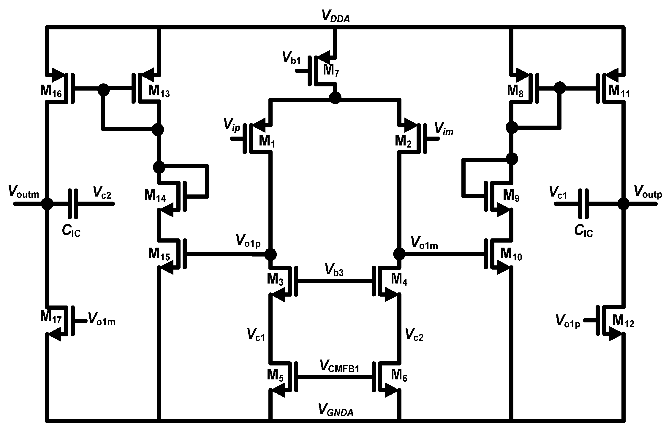
As described earlier in this section, the first integrator plays a dominant role in determining the desired SNR. The first opamp (
A1) is designed for a DC gain of 75 dB and a unity-gain frequency of
fun = 1.5
fs ≈ 10 MHz with higher slewing performance (≈20 V/μs) [
3]. These values are obtained from system-level simulation in our custom developed CT- toolbox (implemented in MATLAB), using a two-pole and single-zero opamp model. Design constraints of the second and third opamp (
A2 and
A3) are relaxed and are designed for
fun = 0.75
fs ≈ 4.5 MHz to consume as low power as possible. The systematic design procedure assumes the adder is ideal. In reality, the adder also introduces excess delay in the loop, due to the finite
fun of the opamp. This excess delay in turn introduces peaking in the magnitude response of the NTF and thus increasing the OBG. To mitigate this NTF peaking,
A4 is designed for
fun = 3
fs ≈ 19 MHz. The power consumption of
A4 is almost equal to that of
A1 as only 60 dB DC gain is used in A
4.
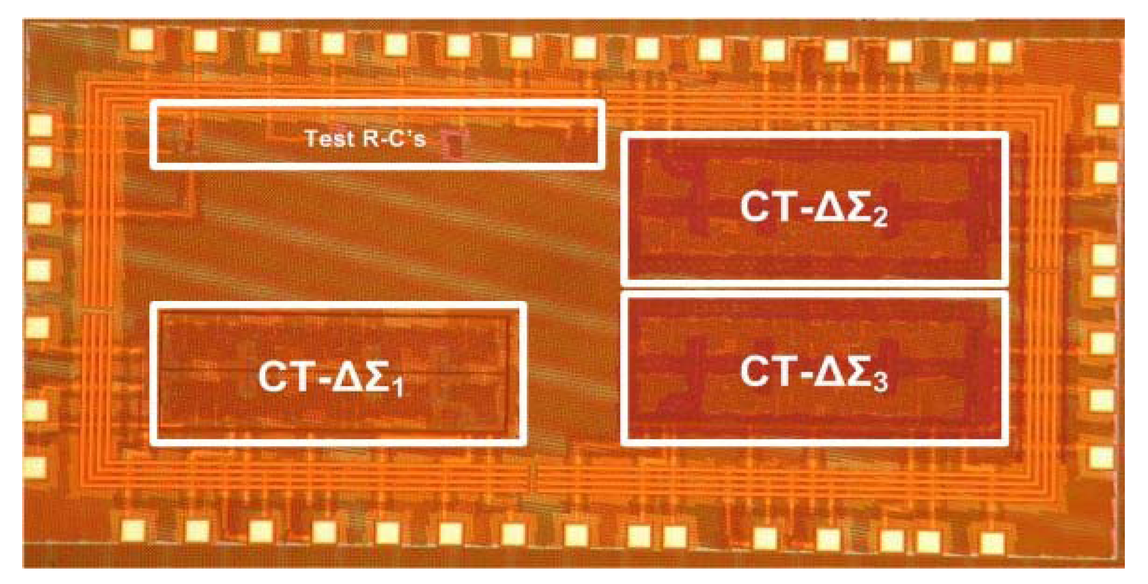
5. Simulation Results
The third-order CT-ΔΣ ADC was designed and fabricated in MIT Lincoln Lab’s experimental 0.15 μm FD-SOI CMOS process.
Figure 9 shows the micrograph of the fabricated chip. Since the FDSOI process did not have well-controlled resistivity and capacitance, three separate ADC layouts were included on the chip. The three designs covered a spread of 50% variation in the RC time-constants. Sixty-four thousand output samples were collected from the modulator in the post-layout simulation.
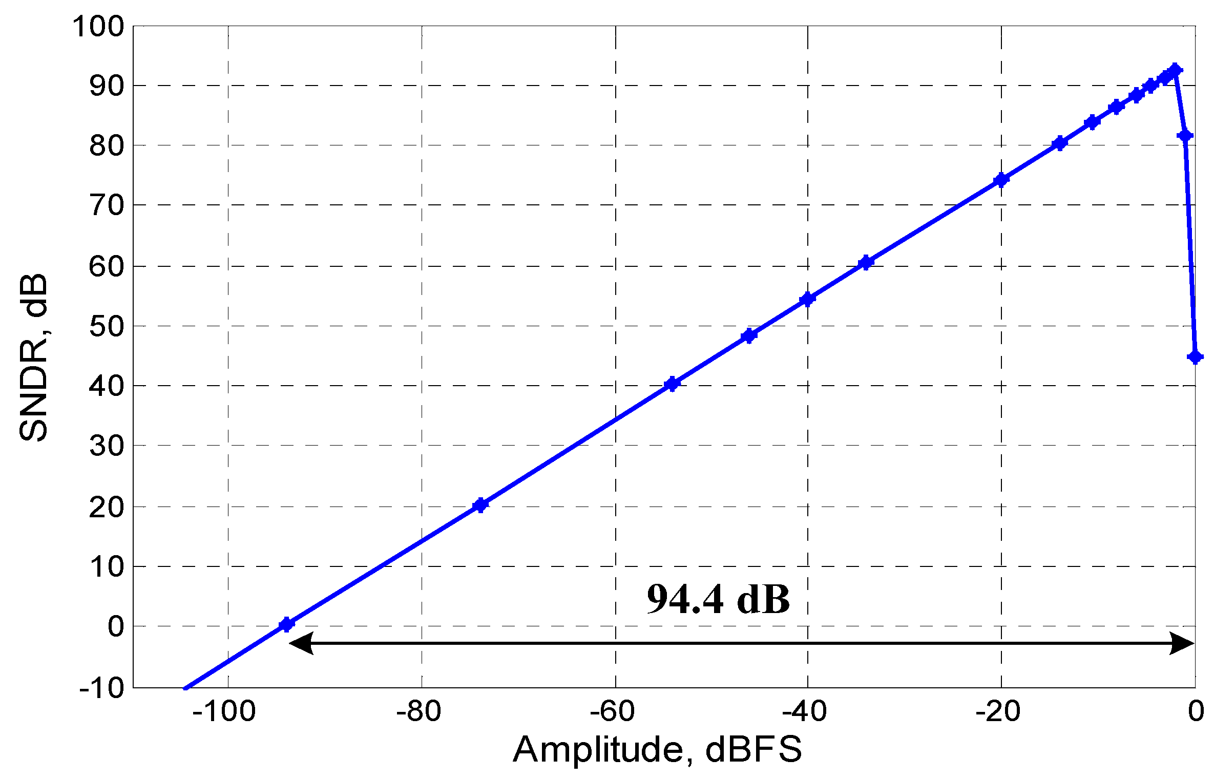
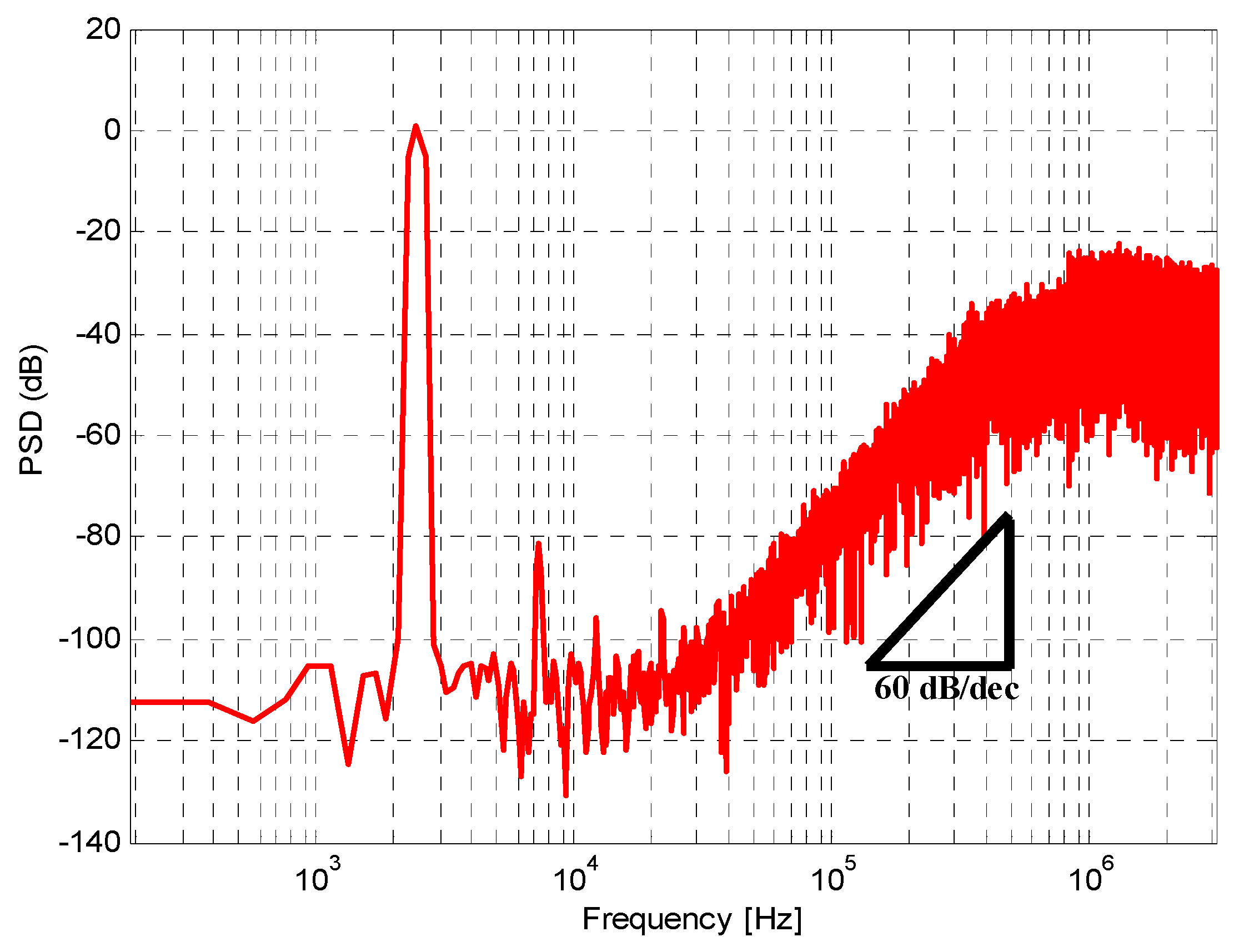
Figure 10 and
Figure 11 illustrate the post-layout simulated signal to noise and distortion ratio (SNDR). The SNDR is measured using a 2.3 kHz input tone. The peak SNDR is close to 92.5 dB and the simulated dynamic range of the modulator is 94.4 dB.
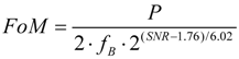
Table 2 summarizes the simulated performance of the modulator. The figure of merit (FoM) of the converter is calculated using power consumption (
P), signal bandwidth (
fB) and SNR by using the relation [
7].
The modulator presented in this paper achieves 0.271 pJ/level.
Table 3 compares the simulated performance of the presented FDSOI design with several continuous-time ΔΣ ADCs from recent literature [
7,
18,
19,
20,
21,
22].
Figure 9.
Fabricated chip micrograph containing the designed CT-ΔΣ ADCs.
Figure 9.
Fabricated chip micrograph containing the designed CT-ΔΣ ADCs.
The chip was wire-bonded in a DIP package, mounted on a PCB and tested. External sinusoidal and clock inputs were applied to the chip and the output samples were collected using a mixed-signal oscilloscope. The experimental testing revealed that the value of resistances and capacitances on the chip deviated significantly from the expected values, resulting in the CT-ΔΣ modulators to be unstable. Our experiments led to the conclusion that at least one of the opamps in the design became unstable due to the compensation scheme breaking down with large process variation. Thus a well-characterized process with stable resistivity and capacitance parameters is necessary for such mixed-signal designs. The design presented in this paper shows significant improvement over several design except for an excellent power-optimized CT-ΔΣ design presented in [
7].
Figure 10.
Simulated spectrum of modulator.
Figure 10.
Simulated spectrum of modulator.
Figure 11.
Simulated SNDR/Dynamic range.
Figure 11.
Simulated SNDR/Dynamic range.
Table 2.
Summary of simulated CT-ΔΣ modulator performance.
Table 2.
Summary of simulated CT-ΔΣ modulator performance.
| Signal Bandwidth/Clock Rate | 6 kHz/6.144 MHz |
| Quantizer Range | 3 Vpp, diff |
| Input Swing for peak SNR | −1.92 dBFS |
| Dynamic Range/ SNDR | 94.4 dB/92.4 dB |
| Active Area | 0.016 mm2 |
| Process/Power Supply Voltage | 0.15 µm FD-SOI/1.5 V |
| Power Diss. Modulator /Reference | 110 µW/20 µW |
| Figure of Merit | 0.271 pJ/level |
Table 3.
CT-ΔΣ modulator performance comparison.
Table 3.
CT-ΔΣ modulator performance comparison.
| Reference | Bandwidth | OSR | Supply Voltage | Technology | Dynamic Range | Power | Peak SNR | FoM (pJ/conv) |
|---|
| This work | 6 kHz | 512 | 1.5 V | 0.15 µm FDSOI | 94.4 dB | 110 µW | 92.4 dB | 0.271 |
| [7] | 24 kHz | 64 | 1.8 V | 0.18 µm | 93.5 dB | 90 µW | 92.5 dB | 0.054 |
| [18] | 24 kHz | 48 | 1.5 V | 0.35 µm | 80 dB | 135 µW | 73 dB | 0.74 |
| [19] | 24 kHz | 48 | 1.5 V | 0.35 µm | 81 dB | 250 µW | 66 dB | 3.07 |
| [21] | 20 kHz | 128 | 3.3 V | 0.35 µm | 106 dB | 18 mW | 99 dB | 6.18 |
| [22] | 20 kHz | 300 | 1.5 V | 65 nm | 95 dB | 2.2 mW | 77 dB | 9.51 |

 , where E[x] is the estimation operator on the discrete-time sequence x[n] [4]. Thus, an effective NTF1(z) is obtained by substituting a suitable value of kq. Figure 3 shows the magnitude response of the modulator NTF fitted to the modulator’s response using the effective quantizer gain kq.


 . This impulse response fitting method breaks down when applied to real integrators with finite op-amp DC gain, non-dominant opamp poles and the presence of opamp zeros. To get the desired NTFeff(z), either the filter coefficients (K) need to be further tuned or the DC gain and the unity-gain frequency (fun) of the opamp must be sufficiently large. The latter will result in an increase in the modulator power consumption [11,16]. Also, in a single-bit single-loop CT-ΔΣ modulator, more than 90% of the power is consumed by the opamp, which is a key design block in the loop-filter. In order to achieve low power consumption in the modulator, the bias currents in the opamps need to be optimized for the given specification. Any power reduction in the opamp impairs the characteristics of the loop-filter and thus impacts the resulting NTF performance. Figure 5 shows the magnitude response of NTF(z) with ideal and real integrators for the same loop-filter. It can be seen that the systematic design method restores the modulator NTF with integrators implemented using real opamps having two poles and a zero. Moreover, it is also essential that the slewing in the opamps is sufficiently limited so as not to degrade the overall modulator linearity.
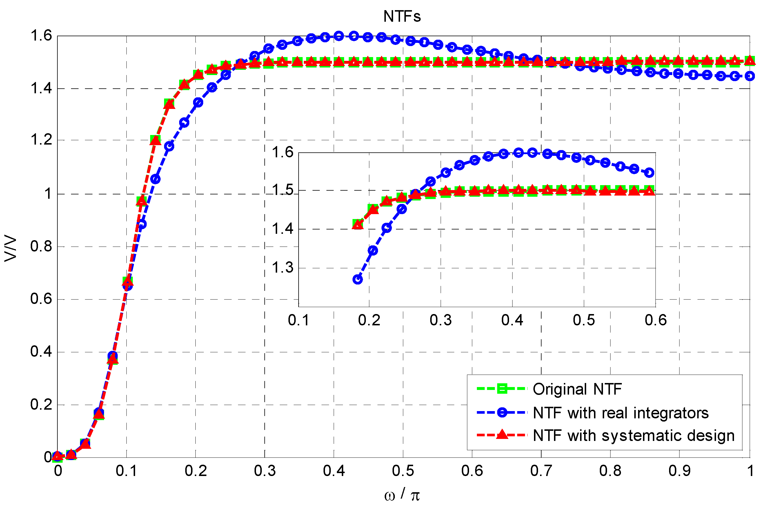
 , where
  and
and  represent the sampled DAC pulse response of direct path and at the output ith integrator (see [11] for details). Table 1 shows the derived loop-filter coefficients for the modulator, before and after systematic design procedure.
 ratio for a given transistor overdrive in the sub-VT regime, and thus lead to lower-power analog circuits when compared to a bulk CMOS process. However, due to the experimental nature of the FDSOI process technology, only typical corner models were available for circuit simulation and the noise parameters were not incorporated in the BSIMSOI Spectre models.