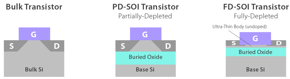
2.1. FDSOI vs. PDSOI vs. Bulk Process
Analog design has been proven robust in standard digital bulk processes for decades, but as the technology migrates to Partially Depleted Silicon-on-Insulator (PDSOI) and then onto FDSOI, an investigation of the merits of FDSOI for analog amplifiers is timely. The merits of the technology are many, from the proven shrinking of the CMOS device, the lower leakage current, less short channel effects (SCE), lower expected
Vth variations due to lower dopant fluctuations, lower voltage supply and thus lower expected power consumptions.
Figure 2 below displays the comparison between bulk PDSOI and FDSOI.
Figure 2.
Comparison between bulk PDSOI and FDSOI silicon processes [
8].
Figure 2.
Comparison between bulk PDSOI and FDSOI silicon processes [
8].
When compared to the PDSOI technology, the FDSOI process is free of the floating body effect and has higher immunity to the kink effect. The kink effect which is due to impact ionization can be observed when a discontinuity occurs in the Ids
vs. Vds curve for higher
Vds voltages in strong inversion, where the current increases at a faster rate beyond a certain
Vds [
4]. This is due to an increase in the body potential, and hence it is more prevalent in PDSOI than in FDSOI. The kink effect needs to be considered in analog design as it may contribute to device
Vth mismatch. With SOI, smaller junction capacitance results in lower leakage current, due to less junction area and the non-existence of a leakage path to the substrate as the bulk is separated from the device by an oxide layer. Steep sub-threshold slope for high gain (and energy efficiency) may therefore be achieved in the FDSOI process which is impossible in the standard bulk process due to the inherent body effect.
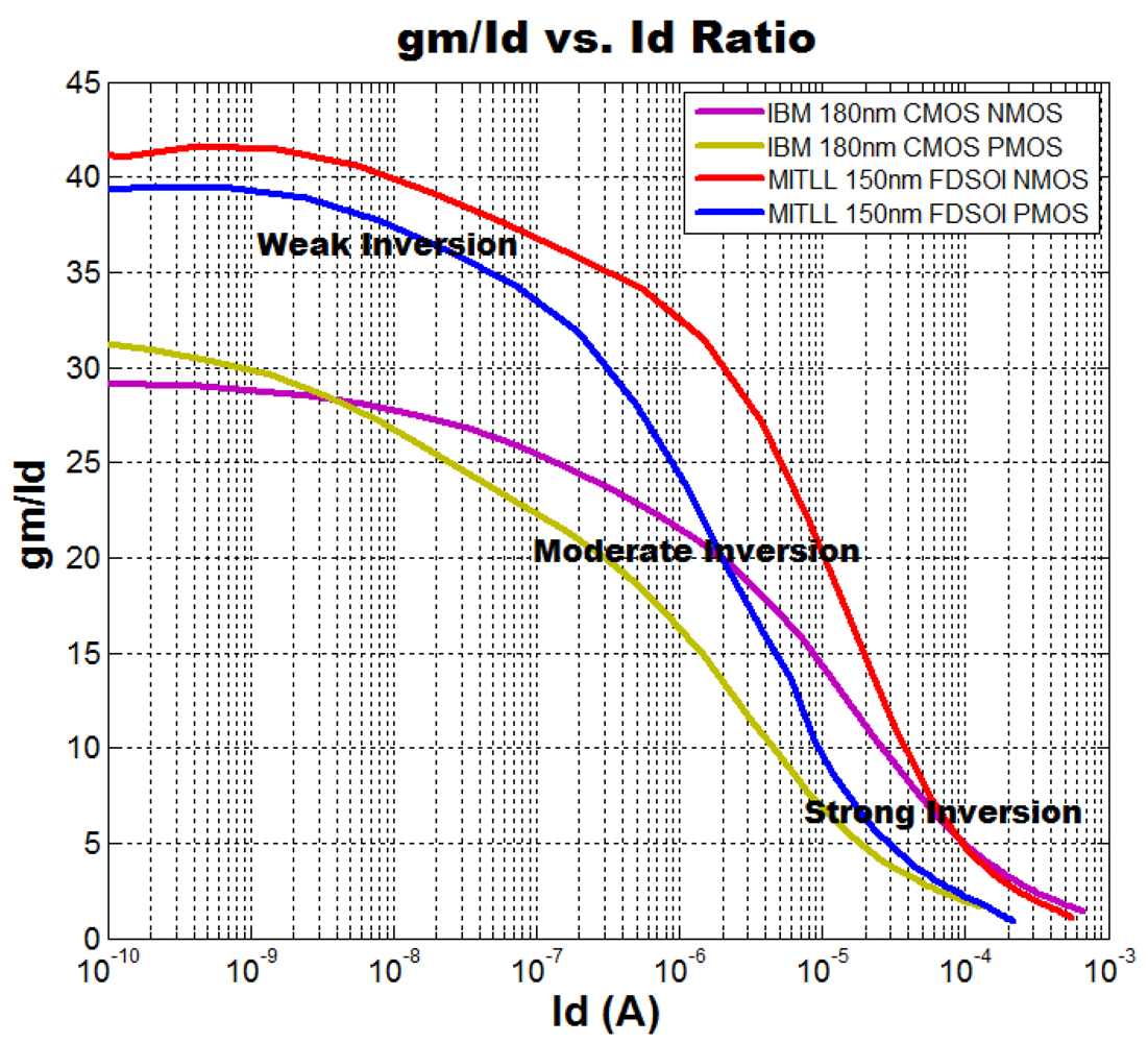
Simulation results were carried out to evaluate the benefit of the MITLL FDSOI XLP 150 nm node process when compared to IBM’s Bulk process at the 180 nm node. The threshold voltages were found to be 0.22 V for the NMOS and 0.27 V for the PMOS in the bulk IBM 180 nm process and approximately 0.45 V–0.5 V in the FDSOI process. This digital process was of interest as, not only was it capable of ultra-low power operation, but it came with available resistors and capacitors that made the biasing and compensation of analog cells possible. The process also claimed an “anomalously steep sub-threshold slope” [
9] and the kink effect was only present above a
Vds of 1.1 V. Keeping devices below that bias voltage could thus minimize any kink effects. The sub-threshold slope and the
gm/
Id ratios were compared for both PMOS and NMOS devices. Both NMOS and PMOS device used have a width of 5 µm and a length of 1 µm. Minimum lengths were avoided to mitigate some short channel effects and because core analog blocks rarely rely on minimum length for matching purposes. From
Figure 1, the
gm/
Id of the FDSOI process is maximized for weak inversion with a max ratio of approx. 42; which is much higher than in the strong inversion region where the
gm/
Id varies between 1 and 10 (
Vgs −
Vth > 0.1 V). When comparing to IBM’s 180 nm bulk CMOS process, the
gm/
Id ratio for very low I
d is 28 for the NMOS and 32 for the PMOS. As displayed in
Figure 1, the FDSOI process proves to be superior at very low Id for both MOS devices that makes it an excellent choice for very low power application.
The sub-threshold slope factor is a significant parameter for the weak inversion operation of a device in the intended V range of operation. Its theoretical lower limit is 60 mV/dec, the slope factor
S can be obtained in the following way [
10]:
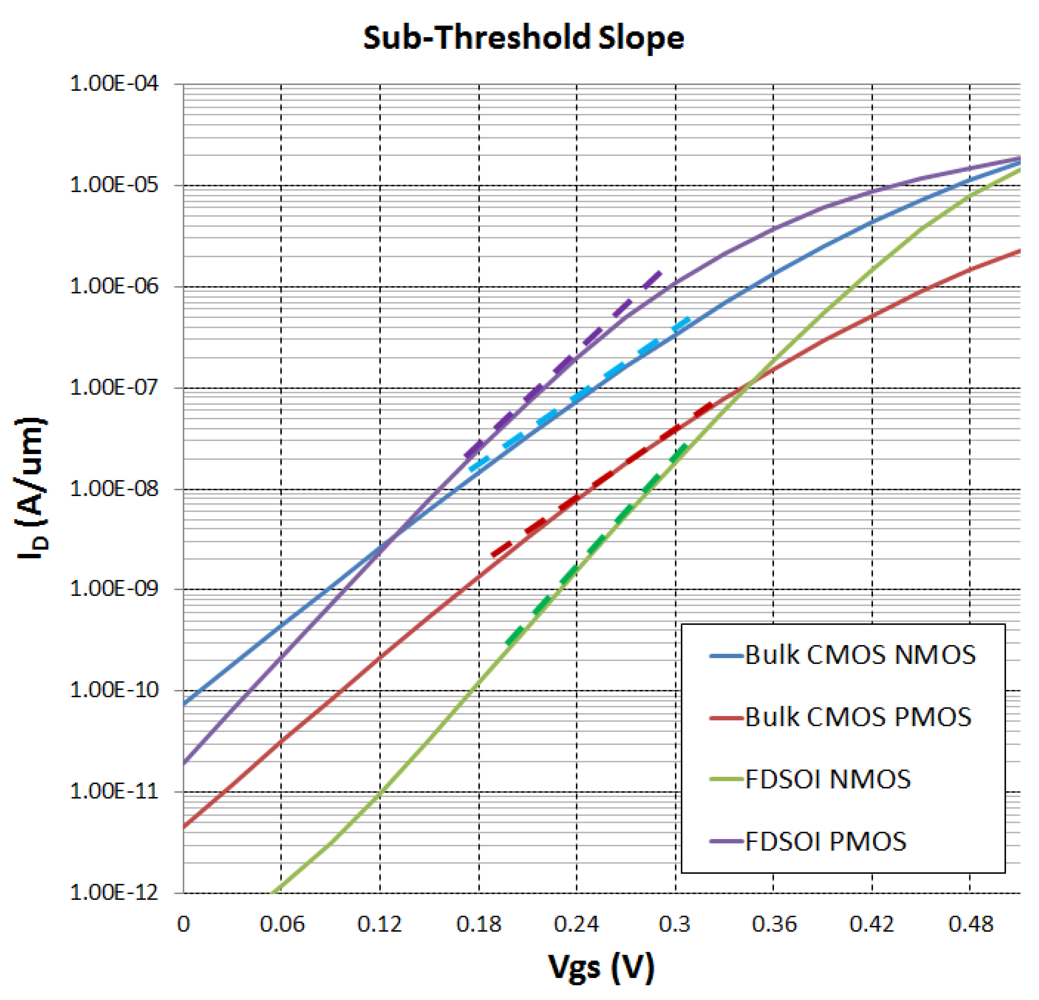
At very low
Vgs of 0.25 V, the slope of the FDSOI process is 50 mV/dev for the NMOS and 52 mV/dev for the PMOS device. For the Bulk process, it is found to be 82 mV/dev for both of the NMOS and the PMOS device.
Figure 3 displays the logarithmic drain current versus
Vgs, displaying that the FDSOI process can provide a superior sub-threshold slope to the 180 nm bulk process at a supply voltage of 0.5 V. As such the FDSOI process was the right choice to investigate sub-threshold analog design.
Figure 3.
Sub-threshold slope of FDSOI and Bulk CMOS devices (VDD = 0.5 V).
Figure 3.
Sub-threshold slope of FDSOI and Bulk CMOS devices (VDD = 0.5 V).
Other advantages of the FDSOI process include reduced crosstalk, elimination of latch-up hazards, better transistor isolation (e.g., noise immunity), lower junction capacitance, and lower source-drain leakage [
6]. These are all due to the reduced coupling to the substrate, as in effect all the devices are isolated from the bulk; and the n-type and p-types devices are more isolated from each other.
The main disadvantages of the FDSOI process when compared to the bulk are the higher costs, which would come down as the process becomes mainstream, the
VT sensitivity to the silicon thickness, the higher series resistor and the floating body effects [
6]. It is however important to realize that, as with any new technology, the total cost of production comes down once the technology becomes mainstream and is being mass produced.
2.2. Design of Two-Stage Differential Pair OTAs
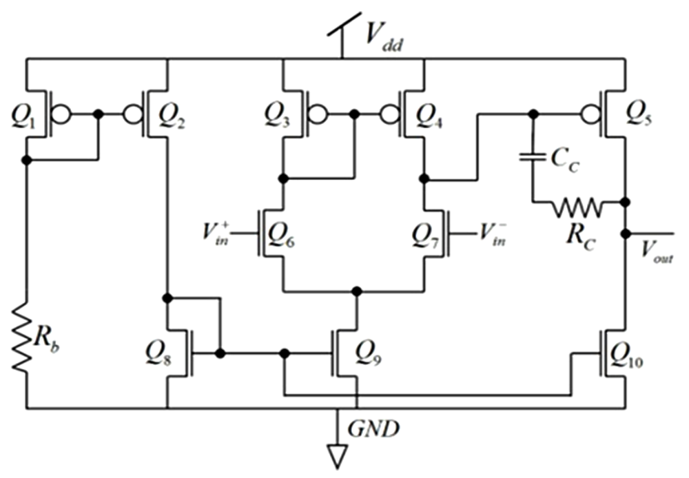
In this paper, our goal was to utilize this advanced FDSOI process to realize a complete operational transconductance amplifier with both PMOS and NMOS input transistors and explore the possibility of aggressively scaling its supply voltage. A PMOS differential pair as well as a NMOS differential pair, as shown in
Figure 4 and
Figure 5, respectively, were designed and optimized to work in the sub-threshold region as well as in strong inversion. Simulation results point to a nominal threshold voltage of approximately 0.45 V–0.5 V for the chosen device sizes. Both designs are two-stage Miller compensated OTAs designed to operate over a 0.5 V–1.5 V range. The PMOS design has its bias current generated off chip, for fine tuning of the device on the bench for optimal operation. Its PMOS differential pair as well as the NMOS load devices use a length of 500 nm, guaranteeing a minimum of matching (proportional to
![Jlpea 02 00155 i002]()
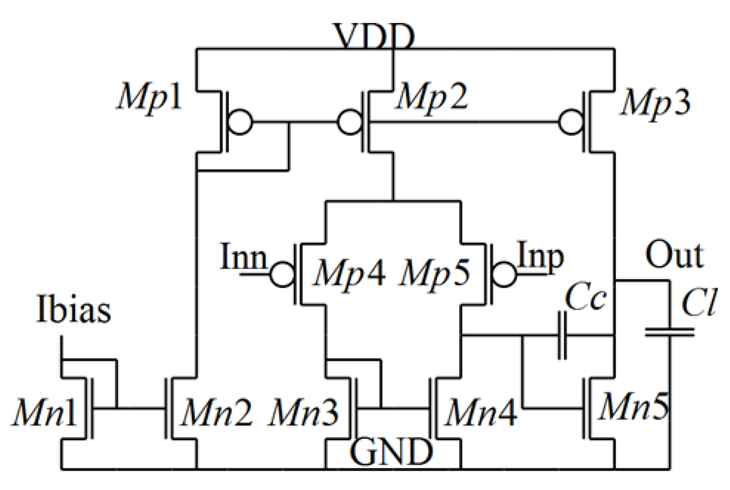
), while minimizing the voltage of operation. The NMOS design has its bias current generated on chip with a 1 MΩ resistor to GND. Its bias is set to (VDD−VGS)/
Rb for the chosen VDD. The NMOS differential pair uses a length of 450 nm and the PMOS load devices use a length of 300 nm.
Figure 4.
PMOS input differential Amplifier.
Figure 4.
PMOS input differential Amplifier.
Figure 5.
NMOS input differential Amplifier.
Figure 5.
NMOS input differential Amplifier.
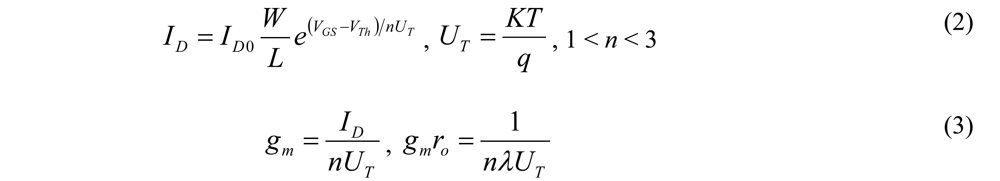
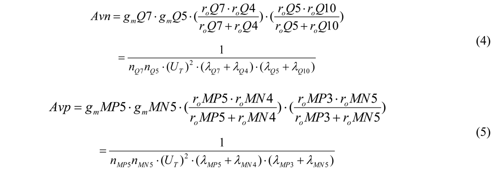
Although the minimal length for this technology is 150 nm, no devices in either amplifier used a length of less than 300 nm. This reduces channel length modulation and increases output impedance. Moreover it provides better matching (process variation is inversely proportional to the area) and minimizes short channel artifacts such as leakage and second order VT dependencies. Only the ESD protections structure at each pin—off PMOS diode to VDD and off NMOS diode to GND—use the minimum length of 150 nm expecting these would turn on first during an ESD event. The equations of intrinsic parameters for a device in sub-threshold region with sufficient drain-source bias are as follow:
Leading to the gain of the OTAs to be the following [
11]:
Since the amplifiers presented here are differential pairs, in layout all the transistors have their source local-body tied to eliminate any potential floating body effects and to ensure better matching, linearity and more stable V
T over voltage [
12], thus minimizing the disadvantages of the FDSOI process from an analog design standpoint. However, we expect that even if such source–body connections were not made, that such metrics would be better than in a PDSOI process. Since these were designed to operate at ultra-low power, self-heating and temperature concerns were not important. Furthermore the kink effects are usually observed at voltages above 1 V, thus the risk of kink effect can be omitted as devices were operating below the voltage of concern and were optimized to work in sub-threshold. In essence, the technology seemed ideal for ultra-low voltage and low power operation.
2.3. Simulation Results
Both OTAs were simulated with Spectre in a Cadence environment using BSIMSOI models with various supplies for various biasing conditions. Bias current is 125 nA for PMOS differential pair OTA.
Table 1 and
Table 2 summarize the various operating conditions. AC responses are presented in
Figure 6 and transient results in
Figure 7. All simulations were carried with 1 pF load.
Table 1.
PMOS differential pair OTA simulation results.
Table 1.
PMOS differential pair OTA simulation results.
| VDD (V) | CM (V) | Gain (dB) | PM (deg) | −3dB BW (kHz) | Total I (µA) |
|---|
| 1.5 | 0.75 | 53 | 80 | 1.4 | 1.1 |
| 1 | 0.5 | 55.8 | 68 | 4.2 | 1.2 |
| 0.75 | 0.38 | 52.4 | 70 | 1.4 | 1.1 |
| 0.5 | 0.2 | 33.7 | 78 | 9.5 | 1.1 |
| 0.4 | 0.15 | 19.7 | 92 | 18.3 | 1.05 |
| 0.35 | 0.15 | 10.1 | 107 | 10.5 | 1.05 |
Table 2.
NMOS differential pair OTA simulation results.
Table 2.
NMOS differential pair OTA simulation results.
| VDD (V) | CM (V) | Gain (dB) | PM (deg) | −3dB BW (kHz) | Total I (µA) |
|---|
| 1.5 | 0.75 | 46.6 | 87 | 45.01 | 7.2 |
| 1.2 | 0.6 | 43.3 | 77 | 29.45 | 4.2 |
| 0.9 | 0.45 | 33 | 69 | 31.3 | 2.2 |
| 0.6 | 0.3 | 9.6 | 80 | 39.6 | 0.8 |
It can be observed that in both designs, the gain decreases with a decreasing supply voltage, falling drastically when the devices run out of headroom and even below the sub-threshold saturation (
VDS < 3 KT/
q ~ 75 mV). It is also worth pointing out that for the NMOS design where the current is controlled off chip; as expected, the gain is higher for a lower current as the devices are biased further in the weak inversion region. For the lowest specified voltage and current bias, the amplifiers can reach an ultra-low power of 0.5 µW; however, the gain is relatively low in the 10 dB range. With a higher current, the gain increases to 46.6 dB for the NMOS pair amplifier and 55.8 dB for the PMOS differential pair. The results are comparable with prior work [
2,
3,
13]. In a standard SOI process, an OTA gain of 44 dB was achieved for a power of 3.6 µW when the supply was 1.2 V [
2], while in another FDSOI 180 nm implementation an OTA with a gain of 64.5 dB when the supplies were ±0.75 V for a current draw of 472 µA and a power dissipation of 708 µW was designed [
13]. What is unique in this paper is that the results show that similar performance can also be achieved in a fully depleted process with potential for even lower power consumption due to better sub-threshold slope.
Neither amplifier was optimized for minimal noise contribution, as the primary goal was to drive the OTAs in deep sub-threshold while consuming ultra-low power. Noise optimization is left for a future exercise. In both designs, the main contribution of noise was flicker noise as the differential amplifier pairs are small: W/L (NMOS_OTA) = 9 µm/450 nm and W/L (PMOS_OTA) = 10 µm/500 nm. For a Supply voltage (VDD) of 1.5 V and a common voltage (Vcm) of 0.75 V, the input referred noise for the PMOS OTA is 89.33 nV/sqrt(Hz) for a bias current of 1 µA and it is 167.2 nV/sqrt(Hz) for a bias current of 125 nA. For a VDD of 0.5 V and a Vcm of 0.15 V, the input referred noise for the PMOS OTA is 99.4 nV/sqrt(Hz) for a bias current of 1uA and it is 163.3 nV/sqrt(Hz) for a bias current of 125 nA. For a VDD of 1.5 V and a Vcm of 0.75 V, the input referred noise for the NMOS OTA is 87.13 nV/sqrt(Hz) and it is 213.7 nV/sqrt(Hz) for a VDD of 0.6 V and a cm of 0.3 V. Noise results are reported at 10 kHz.
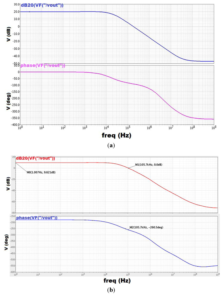
Figure 6.
AC response (a) PMOS differential pair for VDD = 0.4 V, CM = 0.15 V, I bias = 125 nA; (b) NMOS diff pair, VDD = 0.6 V, CM = 0.3 V.
Figure 6.
AC response (a) PMOS differential pair for VDD = 0.4 V, CM = 0.15 V, I bias = 125 nA; (b) NMOS diff pair, VDD = 0.6 V, CM = 0.3 V.
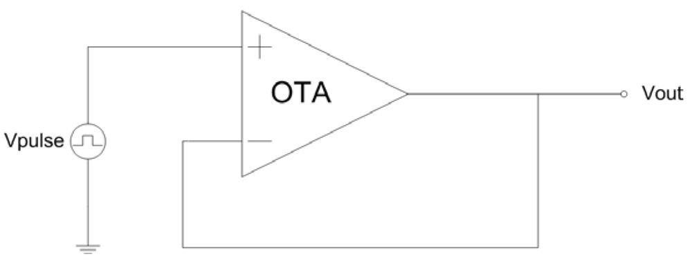
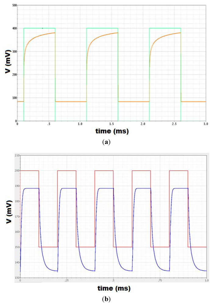
Figure 7.
Transient response (a) PMOS amplifier; (b) NMOS amplifier in unity gain configuration.
Figure 7.
Transient response (a) PMOS amplifier; (b) NMOS amplifier in unity gain configuration.


 ), while minimizing the voltage of operation. The NMOS design has its bias current generated on chip with a 1 MΩ resistor to GND. Its bias is set to (VDD−VGS)/Rb for the chosen VDD. The NMOS differential pair uses a length of 450 nm and the PMOS load devices use a length of 300 nm.

