Simulation and Optimization of Film Thickness Uniformity in Physical Vapor Deposition
by
 , , ,
, , ,
Ben Wang
1,2, 
Xiuhua Fu
1,*,
Shigeng Song
2,*,
Hin On Chu
2,
Desmond Gibson
2,
Cheng Li
2,
Yongjing Shi
3 and
Zhentao Wu
2 1
School of OptoElectronic Engineering, Changchun University of the Science and Technology, Changchun 130022, China
2
Institute of Thin Films, Sensors and Imaging, School of Engineering and Computing, University of the West of Scotland, Paisley PA1 2BE, UK
3
School of Material Science and Engineering, Chongqing University of Science and Technology, Chongqing 401331, China
*
Authors to whom correspondence should be addressed.
Coatings 2018, 8(9), 325; https://doi.org/10.3390/coatings8090325
Submission received: 8 July 2018
/
Revised: 30 July 2018
/
Accepted: 12 September 2018
/
Published: 16 September 2018
(This article belongs to the Special Issue Applications of Optical Thin Film Coatings)
Abstract
:Optimization of thin film uniformity is an important aspect for large-area coatings, particularly for optical coatings where error tolerances can be of the order of nanometers. Physical vapor deposition is a widely used technique for producing thin films. Applications include anti-reflection coatings, photovoltaics etc. This paper reviews the methods and simulations used for improving thin film uniformity in physical vapor deposition (both evaporation and sputtering), covering characteristic aspects of emission from material sources, projection/mask effects on film thickness distribution, as well as geometric and rotational influences from apparatus configurations. Following the review, a new program for modelling and simulating thin film uniformity for physical vapor deposition was developed using MathCAD. Results from the program were then compared with both known theoretical analytical equations of thickness distribution and experimental data, and found to be in good agreement. A mask for optimizing thin film thickness distribution designed using the program was shown to improve thickness uniformity from ±4% to ±0.56%.
1. Introduction
Physical vapor deposition (PVD) is an important family of techniques for thin film processes. Applications of PVD deposited thin films include: optical band-pass filters [1], surface enhanced Raman spectroscopy [2], hydrophobic coatings, and sensors [3]. PVD involves the conversion of a source material into the gas phase, which is then deposited onto a substrate surface [4] and can be achieved through either evaporation or sputtering [5]. The advantages of evaporation based PVD techniques are that these films are of higher purity and allow better control over film thickness [6,7]. Sputtering involves using ionized species that are accelerated to the target, once these ionized species hit the target surface they eject target material that arrives at the substrate to form a desired thin film [8]. Sputtering is widely used for its low production cost and good repeatability [9]. Regardless of technique or application, the uniformity of film thickness is very important. This is especially true for high precision multilayer films such as: mirrors used in gravitational wave detection [10], large area substrates for applications including: AR coatings [11], optical filters [12], high laser damage threshold, and laser protection filters [13]. As batch production and large-area manufacturing become necessary for cost reduction, tolerances for film thickness distribution are reduced significantly and film uniformity gains more attention. Film thickness uniformity is influenced by the configuration and environment between the material source and the substrate, as well as the source emission characteristics [14]. These factors include: substrate holder geometry, vacuum pressure, system temperatures (i.e., substrate and material flux temperatures), and angular configuration of the deposition material to the substrate [15]. Separate studies of these factors were carried out by various researchers: the emission characteristics of evaporation sources were summarized by Aaron and Charles [16]; film thickness distributions of the flat plate, spherical surface and planetary substrate holders of evaporation sources were investigated in [17,18,19,20,21]; the parameters for sputtering PVD systems were studied by [14,22,23,24]; and Villa et al. and Hsu [25,26] studied and simulated mask designs for thin film depositions, particularly for sputtering depositions. However, there has yet to be a systematic review of techniques, methods, and modelling theories for producing higher uniformity coatings in PVD systems. Therefore, this paper presents a systematic review of theories, techniques, simulations, and design approaches for improving coating uniformity in PVD configurations, including both evaporation and sputtering methods. Then using the modelling techniques and theories proposed in this review, a program for modelling is written using MathCAD. Simulated results are compared against the literature as well as our experimental data to validate the models.
2. Source Emission Characteristics and Thin Film Thickness Distribution
2.1. Emission Characteristics of Evaporation Source
Holland and Steckelmacher pointed out in 1956 that the evaporation characteristics of sources are mainly divided into two types: one type is a point source that uniformly emits vapor molecules in all directions, the other type is the small surface source (approximated point source) that emits in a cosine distribution that follows Knudsen’s laws [16,27]. Due to the size of the evaporation source, there is no ideal point source model for uniformly emitting vapor molecules in all directions. For the small-surface source, typically when the distance between the evaporation source and the substrate is relatively long compared to the surface area of the evaporation source, the evaporation source can be approximated to a point source obeying the cosine distribution (Knudsen). In addition to these two types proposed by Holland and Stecklemacher, another type of source emission characteristics is extended sources where the sources have large surface areas. This can be the case when the distance between the substrate and the evaporation source is relatively short compared to the surface area of the evaporation source [28].
2.1.1. Small Surface Source (Approximated Point Source)
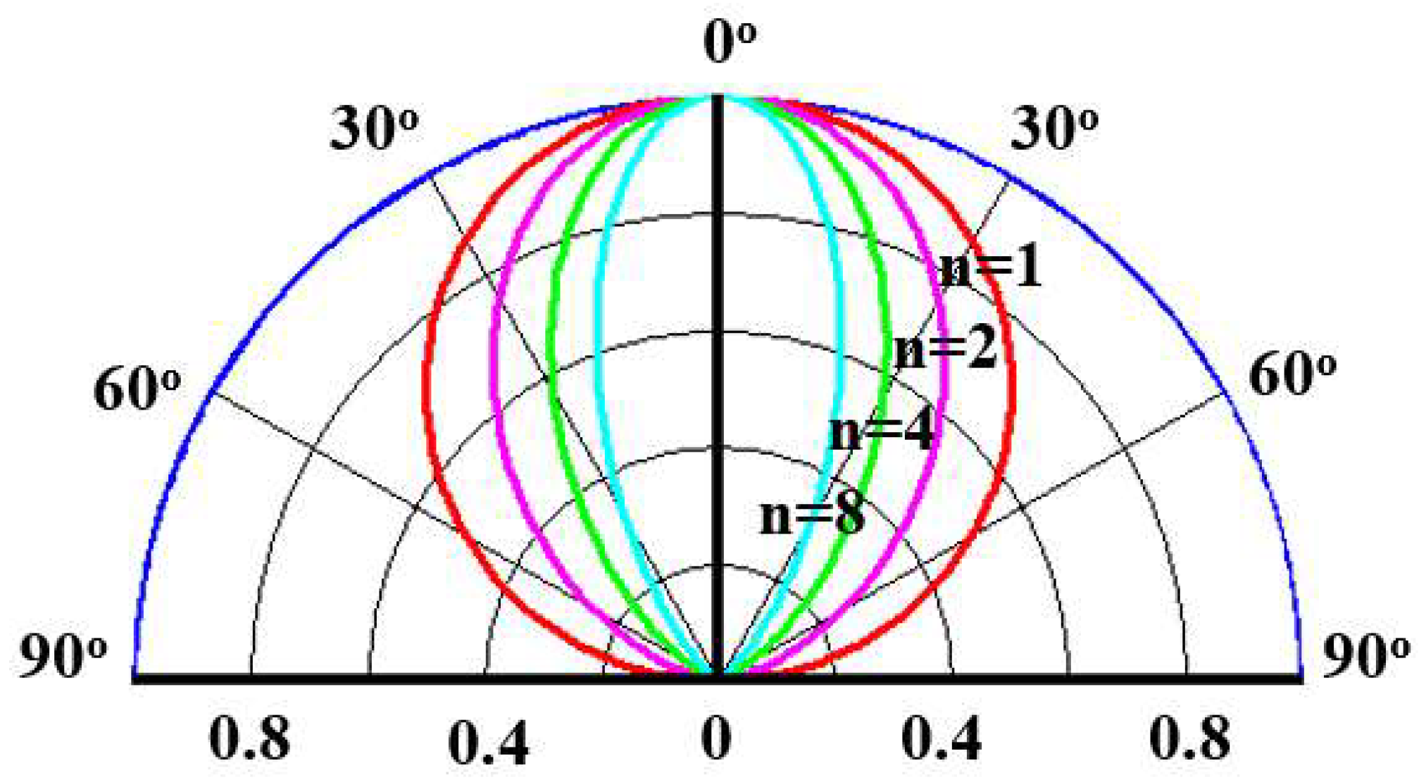
When dealing with a small surface source (approximated point source), the surface of evaporation source can be considered as a sum of infinitesimal unit areas. Each of these integral areas on the surface contributes to the material flux, which forms a leaf-shaped evaporation characteristic along the surface normal. No evaporation occurs when angle is at 90°. Due to the mutual collisions between evaporated materials near the surface during heating, evaporation characteristics do not fully obey the distribution. In many cases, these characteristics are consistent with , where n is a real number [29,30]. This amended cosine distribution may be lower or higher than the original cosine distribution, depending on material and environmental factors. As shown in Figure 1, the value of n determines the angular distribution of the leaf-shaped vapor cloud and the material flow: the larger the value, the better the vapor directionality. n is related to the geometry of the crucible used for evaporation, defined as the ratio of the crucible depth to the surface area of the crucible. For example, deep narrow crucibles possess a large n value [31].
2.1.2. Extended Source
Extended sources are equivalent to the superposition of points on the source surface, that also follows either or distributions. Superposition is dependent on crucible shapes, expressed as: or .
2.2. Virtual Electron-Beam Evaporation Source
At high evaporation rates, in electron-beam (EB) deposition, the vapor formed just above the liquid material is a high-pressure viscous cloud of hot evaporant. The complex energy transfer between electronic excitation and translational motion of vapor atoms in this region, and its effect on flow to the substrate has been modelled for EB evaporated titanium by Balakrishnan [32]. As suggested by Figure 2, the region beyond this dense cloud is at much lower pressure and it is assumed that molecular flow prevails here [5]. Thus, instead of evaporant particles being released from various points on the flat source surface, they appear to originate from the perimeter of this spherical viscous cloud. The ratio of hv/h, which depends on the evaporation rate, is generally 0.7 for typical deposition systems [30]. Two main challenges in electron beam evaporation are electron-beam curling and non-uniform beam density. For electron-beam curling, if the source is not hit by the electron-beam vertically, this makes film thickness predictions difficult. As the electron trajectory curls, material flux distribution from the source will change with time. To address these issues, electron-beam spot diameters and implementing sweeping can optimize film thickness predictions. This configuration prevents material spitting and tunneling into the crucible. Beam sweeping improves the material utilization during deposition [28,33].
2.3. The Emission Characteristics of Sputter Sources
For sputtering thickness distribution simulation, the angular distribution of sputtered atoms needs to be considered. The emission angular distribution is a function of the incident angle of the bombarded ions [34]. Incidence angle of bombardment is mostly at positive angles to the target surface normal. By considering particle collisions and a turbulent electric field, a mean incident angle of 7.95° to the surface normal was obtained using Monte Carlo simulation [35,36]. The incident particle impacts the surface or near-surface atoms of the solid with sufficient energy to break bonds and dislodge atoms. During this process, one or more atoms are sputtered from the target [24,37]. Therefore, the more complex cosine distribution (where A, B, n, and m are all adjustable parameters) is needed for the emission characteristics of a sputtering source [38]. The emission characteristics of the sputtering source behave similarly to Knudsen's laws and in order to simplify the calculation, the approximation is used [12].
The emission characteristics of the source are summarized in Table 1.
2.4. Thin Film Thickness Distribution
2.4.1. Thin Film Thickness Distribution of Evaporation Source
Before calculating the film thickness, three assumptions are made:
- The pressure at which the process is taking place is low enough to ensure that no collisions occur among the vapor and other particles, i.e., the mean-free paths are significantly larger than the dimensions of the deposition system.
- The intensity of the emission of vapor from the source can allow for collisions among the vapor molecules in an extended region in the vicinity of the source.
- Depending on the material undergoing evaporation, the sticking coefficient (Sc) of the vapor molecules can be ≤1 [39], where the sticking coefficient refers to the ratio of number of atoms stuck on the surface to the total number of atoms that impinge upon that surface during the same period of time.
The evaporation in the dω range is
where dM is the total mass of the evaporated material on the infinitesimal area “ds”, m is the total mass of the evaporated material and C is a proportionality constant which can be calculated by integrating Equation (3). Let the accepting (substrate) surface be a sphere and the evaporation source is at its center, thus , , integrate on a sphere:
Calculation reveals , therefore:
t is the film thickness, is the density. The film thickness of the point source () can be expressed as:
For small-surface evaporation sources, the vapor emission characteristics are directional, the emission limits are hemispheres, and the evaporation source is assumed to be at the center of the sphere so that θ = 0, which is integrated in the hemisphere:
From Equation (7), . This kind of surface source is consistent with cosine law, considering the directionality of the surface source emission, the deposition quantity on ds is:
Thus for the small surface source, the thickness is:
Due to particle collisions in the region near the evaporation source, the actual emission characteristics do not fully conform to the distribution, in many cases they are consistent with the distribution.
For small surface sources, after amendment:
The above equation approximates the evaporation source as point source. Commonly used sources in thermal evaporation and EB evaporation are the molybdenum boats and crucibles. As shown in Figure 4, if more precise calculation is needed, integral calculation of the extended source area is needed [39]:
Q is a coefficient determined from the experiments, is the source area.
Detailed analytical formulas are given by Villa [39] for different shapes of regions such as rectangular, ellipsoidal, and spherical concave and convex sources.
2.4.2. Thin Film Thickness Distribution of Sputtering
Film thickness uniformity is affected by the magnetron sputtering source, target geometry, distance between target and substrate, as well as the relative motion between the target and substrate [40]. Magnetron sputtering is generally performed at a relatively high pressure (0.5–1.5 Pa). In this condition, material from the target surface to the substrate is subject to multiple collisions with residual gas particles. However, because the sputtered materials are typically around two orders of magnitude higher than the energy of the residual gas molecules; changes in the velocity and direction of the sputtering molecules can be ignored [41], and the cosine law still applies for this type of deposition.
Before calculating the film thickness, three assumptions are proposed [42]:
- The incident ion is concentrated in the area near the surface of the target, which is accelerated by the electric field to increase the energy. The electric field on the surface of the conductor is always perpendicular to the surface of the conductor, so that the ion is aligned with the target’s surface normal. Therefore, it is assumed that ions bombard the target surface at its normal.
- Collision between the sputtered thin film atoms and the working gas/ions can be neglected.
- Once material is deposited on the substrate, there is no diffusion motion. They stop and become part of the film surface.
Replace the in Equation (11) to (where A, B, n, and m are all adjustable parameters) for sputtering processes, and then simplify this expression to (where is an adjustable parameter) to obtain Equation (12). Due to the large target area, the area of the target cannot be ignored and the target area (q(x, y)) needs to be integrated.
Due to the magnetic field distribution, the sputtering yield of the sputtering source is mainly a circle or a racetrack area, as shown in Figure 5.
Thin film thickness with different types of sources is summarized in Table 2.
3. Calculation of Film Thickness of Substrate Holder on Various Configurations
The film thickness distribution of various geometric configuration of the deposition equipment is summarized as follows. For ease of calculation, the following calculation assumes n to be 1.
3.1. Relative Film Thickness Calculation of Evaporation Source
3.1.1. Flat Plate Substrate Holder
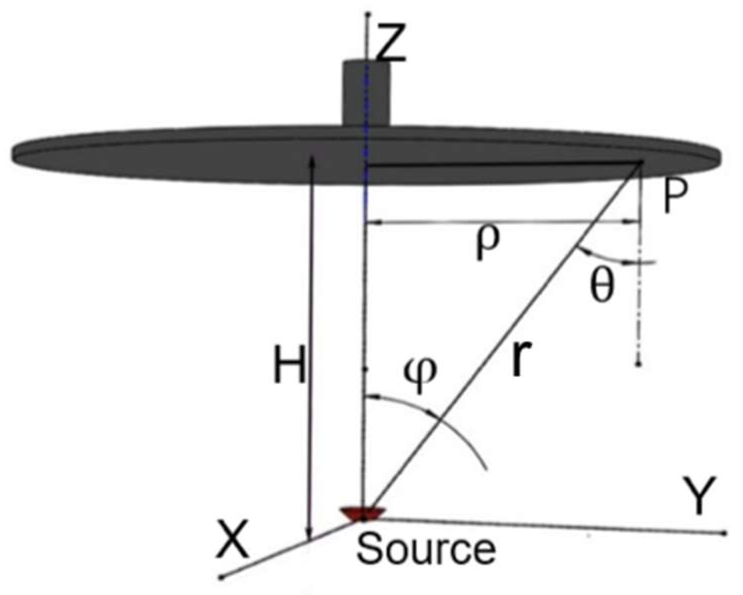
For a simple case of a flat plate held directly above and parallel to the source, the angle is equal to the angle θ and the thickness is as follows [43].
From Figure 6, it can be seen that , and these are substituted into Equation (6) to obtain the film thickness distribution of the point source:
The point source film thickness at the center point can be expressed as:
Therefore, the relative film thickness distribution of point sources is:
, , are brought into Equation (9) to obtain the small surface source (approximated point source) film thickness distribution:
Therefore, the relative film thickness distribution of the surface source is:
Figure 7 shows calculated film thickness distributions on a flat substrate holder for a point source and a small surface source, respectively. It can be seen that these two type sources are not good for the film thickness uniformity on the planar substrate. Thus, this geometric configuration is not suitable for optical films requiring higher uniformity, unless the substrate is very small and is placed in the center of the substrate holder [44].
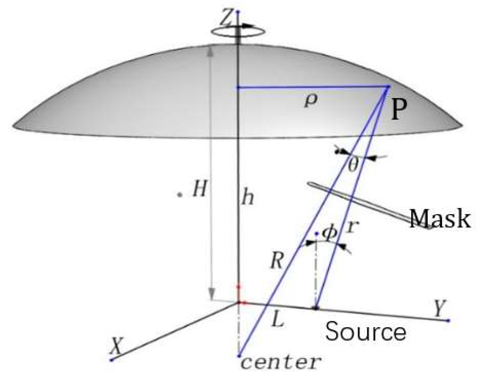
3.1.2. Spherical Substrate Holder
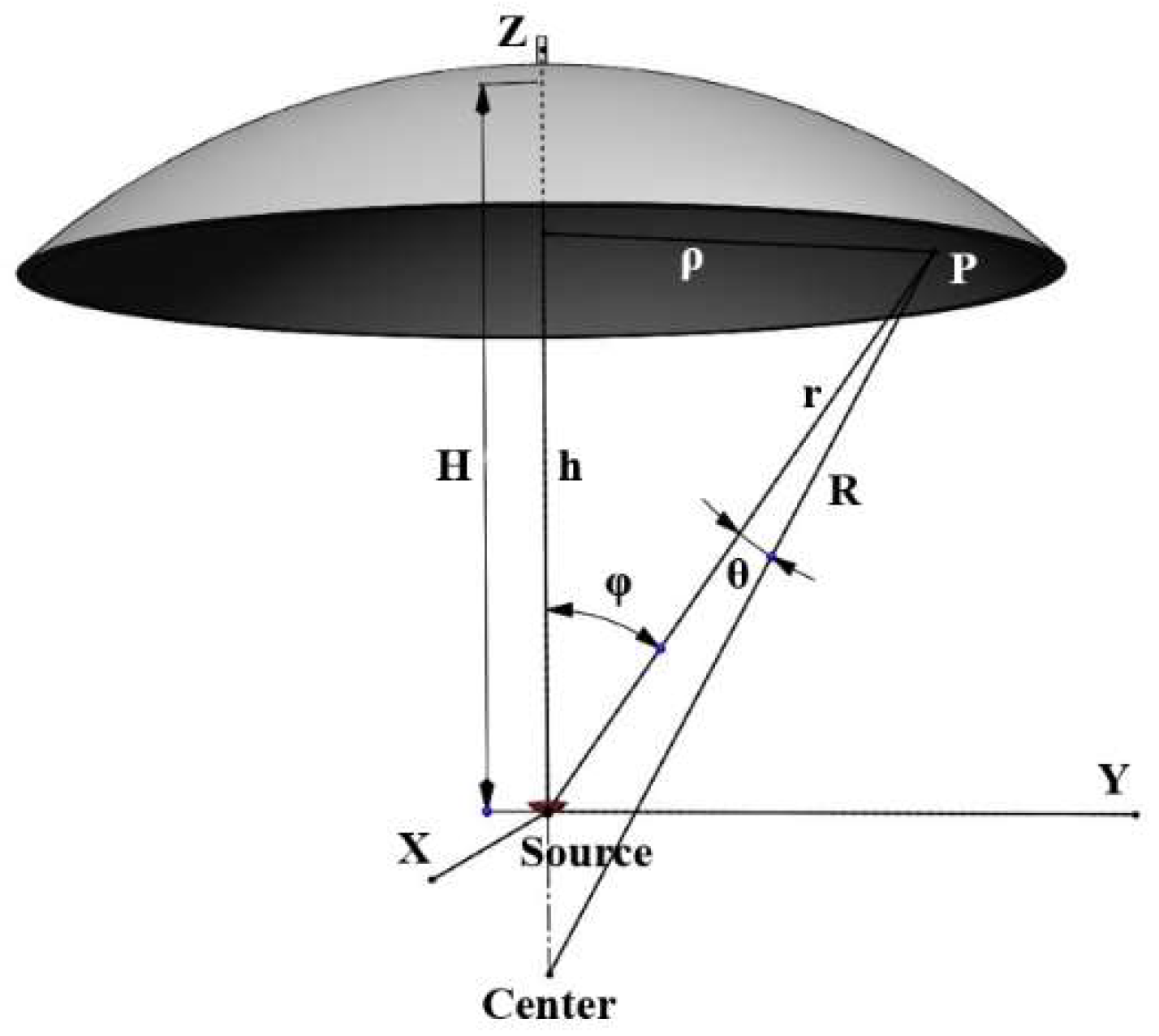
A slightly better arrangement that can sometimes be used is a spherical geometry where the substrates lie on the surface of a sphere. Similar to the flat substrate holder, the derivations are also done for a spherical holder. Equation (18) shows various parameters, as described in Figure 8, which are useful for the following derivations:
Put Equation (18) into Equation (6) to get the equation for point source thickness, , and divide it by the thickness at the center point, , to get the equation for relative film thickness for the point source:
Put Equation (18) into Equation (9) to get the small surface source thickness equation, , and divide it by the thickness at the center point, , to get the relative film thickness equation for the small surface source, simulations for different values of H/r are shown in Figure 9.
A point source will give uniform thickness of deposit on the inside surface of a sphere when the source is situated at the center (Equation (19)). It can be shown that the small surface source will give uniform distribution similarly when it is itself is made part of the surface [44].
3.1.3. Rotating Planar Substrate Holder
It can be seen from the film thickness distribution of the planar and spherical substrate holder that the thickness uniformity of these two configurations is relatively poor and is not suitable for depositing high-precision or large-size optical films. To obtain better film thickness uniformity, the method of rotating the substrate holder can be adopted. The configuration of the plane rotation substrate holder is shown in Figure 10. Deposition equipment with multiple evaporation sources has been gaining recent attention, as this method with rotating substrate can achieve improved uniformity when more than two evaporation sources are used simultaneously. However, the above described spherical substrate holder can achieve good uniformity only at a specific evaporation source position, so substrate rotation must be used when depositing a multilayer optical film [45]. Here, as illustrated in Figure 10, describes the case for a rotating planar substrate holder and the variables are given in Equation (21).
Put Equation (21) into the point source equation and integrate the angle between the normal of the source and the line between the source and point P() to get the thickness equation for the point source:
Assume:
Apply integration:
E(k, π/2) is the second type of elliptic integral, for which the value can be found in a mathematical handbook. The film thickness equation for the point source is:
Film thickness at center point of the substrate holder is:
Since E(0, π/2) = 1.5708, the relative thickness distribution of the point source becomes
Or for the small surface source, integration of the point source through the small area is required, thus bring Equation (22) into Equation (9) to get:
Applying this integration
The thickness expression for the small surface source is:
Thus the relative distribution (to the central position of substrate holder) of the small surface source can be expressed as:
Relative thickness distribution of a rotating planar substrate holder for various H/L values is illustrated in Figure 11a. For example, for a small-surface source, the optimal value of H/L varies with /H when L = 200 mm. In order to good uniformity in the area of < 50 mm (thus for approximately is 0.178 for H/L = 1.405 and L = 200 mm), the best value results are obtained when H/L = 1.405 and the film thickness uniformity error is 0.04% (Figure 11b). Whereas when = 100 mm ( approximates to 0.373 for H/L = 1.34 and L = 200 mm), the optimum value for H/L is 1.34 with a 0.3% uniformity error (Figure 11b). In order to optimize uniformity with a rotating planar substrate holder, the substrate should be placed as centrally on the substrate holder, the substrate should be placed in the center of the substrate holder where possible. If H is allowed to increase, positioning the evaporation source away from the center also improves the uniformity; when H is fixed (typical situation for real circumstances) and a larger deposition area is demanded, then the evaporation source can be moved outwards for a bigger substrate with a compromise in film thickness uniformity. To reduce the effects of this compromise, a correction mask can be applied to improve film thickness uniformity.
3.1.4. Rotating Spherical Substrate Holder
Similarly, derivations for a rotating spherical substrate holder are done. The parameters for thickness uniformity modelling of this configuration are shown in Figure 12 and expressed as:
Put Equation (32) into Equation (6) to get the thickness expression for the point source:
Because:
The point source thickness expression becomes:
F(k, π/2) is the first type elliptic integral, thus for the small surface source:
Because:
Finally, the expression of the film thickness of the small surface source is:
Because , sin = , cos = , the relative film thickness expression for the small surface source can be written as:
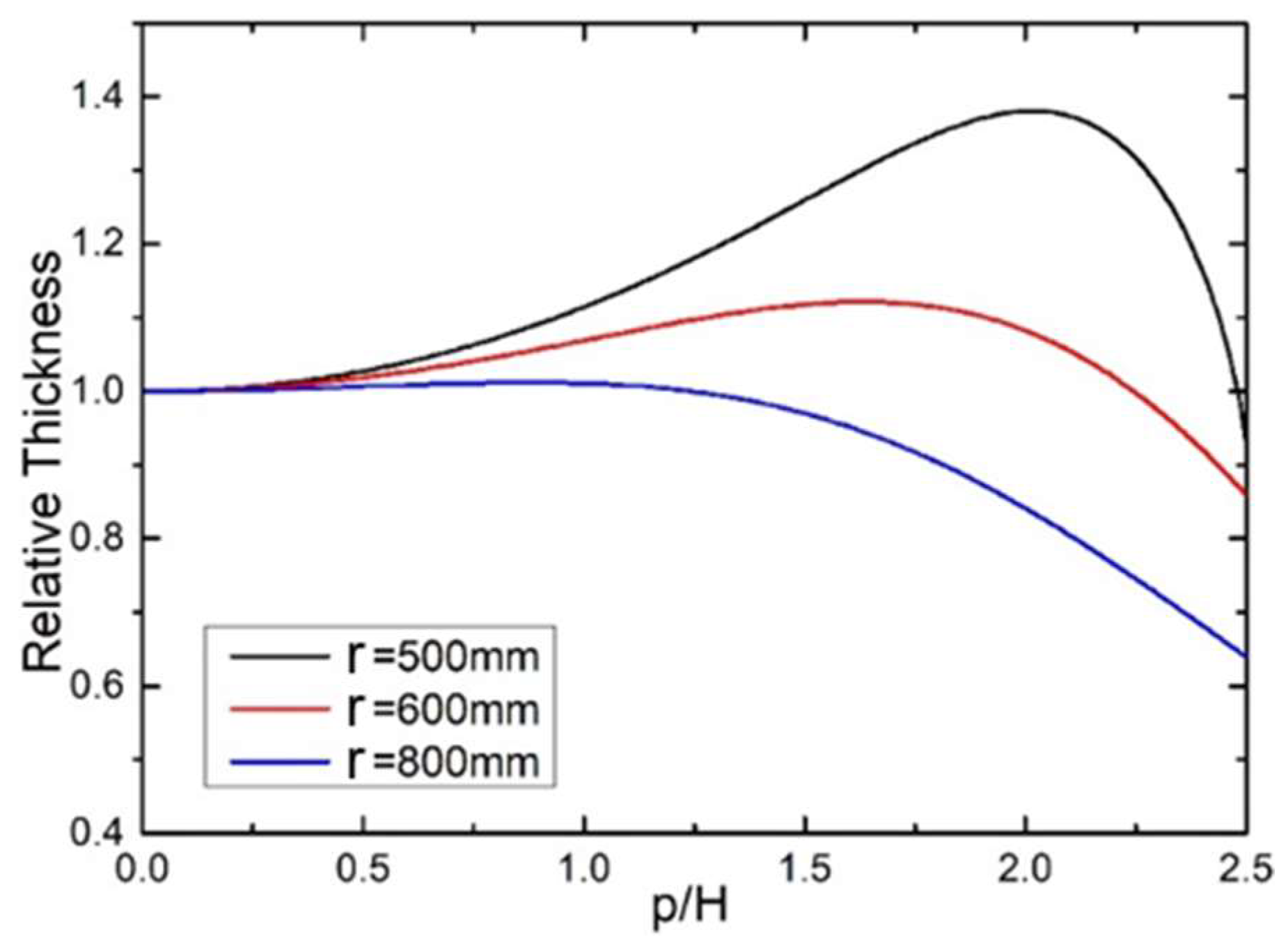
Figure 13 is the thickness distribution of a rotating spherical substrate holder. For small-surface sources, when the radius of curvature is 500, 600, and 800 mm (L = 200 mm), when H/L = 1.90, the thickness error is 0.06%, 0.04%, and 0.03%, respectively; all within the range of = 100 mm [46].
Recent decades have seen the demand for more high uniformity optical coatings, such as those used in the LIGO collaboration for their gravitational wave detectors [47]. These applications tend to require more accurate film deposition control. Planetary substrate holder configurations are becoming a popular option, because film thickness uniformity can be improved. However, analytical solutions (equations) for the planetary substrate holder are difficult to obtain, so this paper uses MathCAD programming to model and calculate the relative distribution of film thickness in Section 5.1.
3.2. Relative Film Thickness Calculations of Sputtering Sources
3.2.1. Planar Substrate Holder with Rectangular Sputtering Target
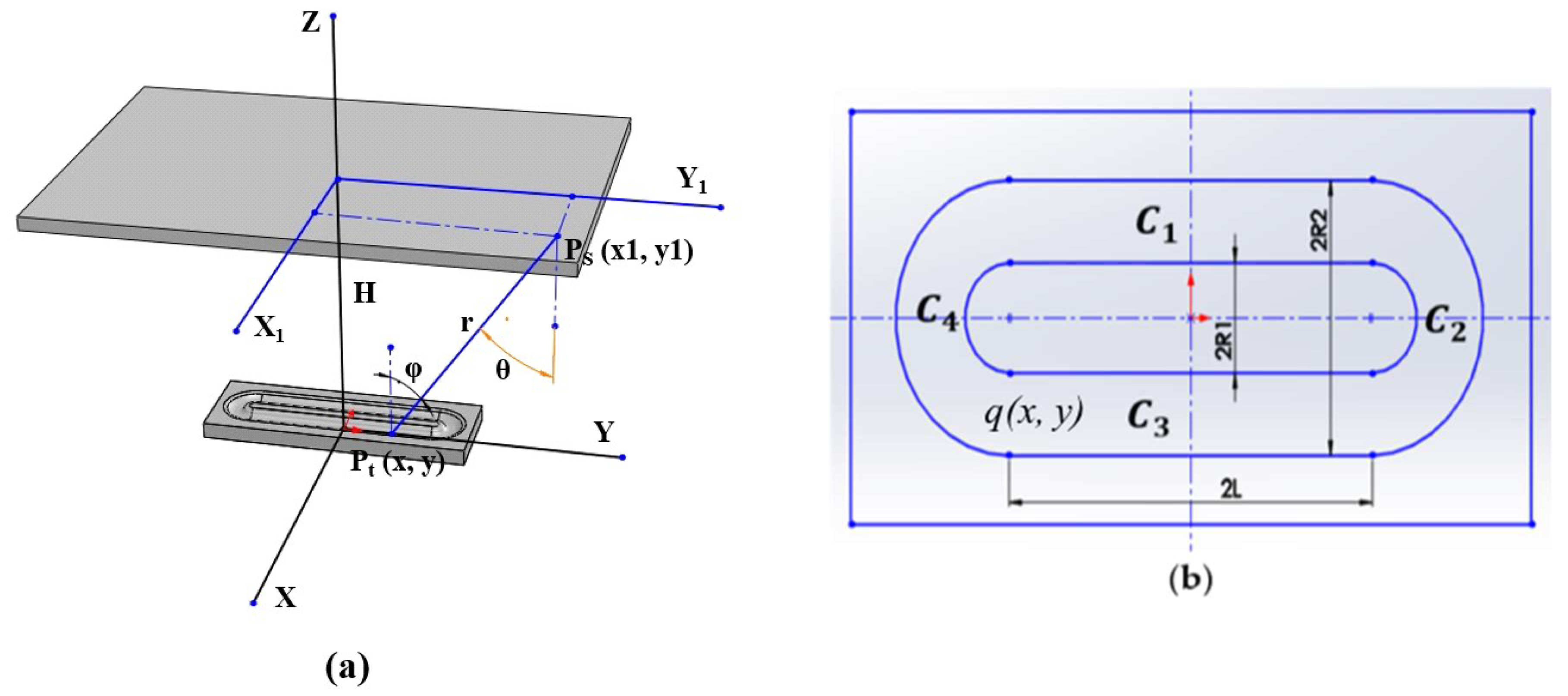
The parameters for thickness uniformity modelling are shown in Figure 14 and expressed as:
The thickness distribution for this sputtering source is:
The area of the sputtering source/target q(x, y) is shown in Figure 14 establishing the coordinate axis with the origin at the center of the target, the target can be divided into four regions . For the convenience of calculation, assume n = 1, = 0.
Integrate the areas of the two rectangles (, ), the deposition thickness at the Ps point (x1, y1) on the substrate can be obtained as Equations (42) and (43), with the rectangular integral areas being : , and : , respectively.
Then integrate the two half-ring sputtering areas and perform coordinate transformation, for the right semicircle region , , the film thickness distribution is expressed in Equation (44), with the semicircle integral area being : ,
Similarly, for the left semicircle region , , with semicircle integral area being : , , the film thickness distribution is:
The total film thickness is the sum of thicknesses of the four regions: .
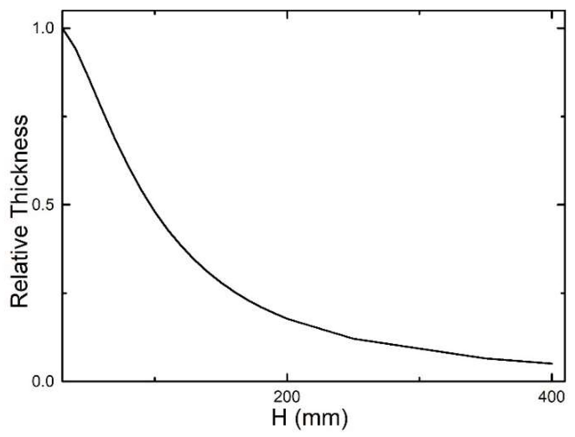
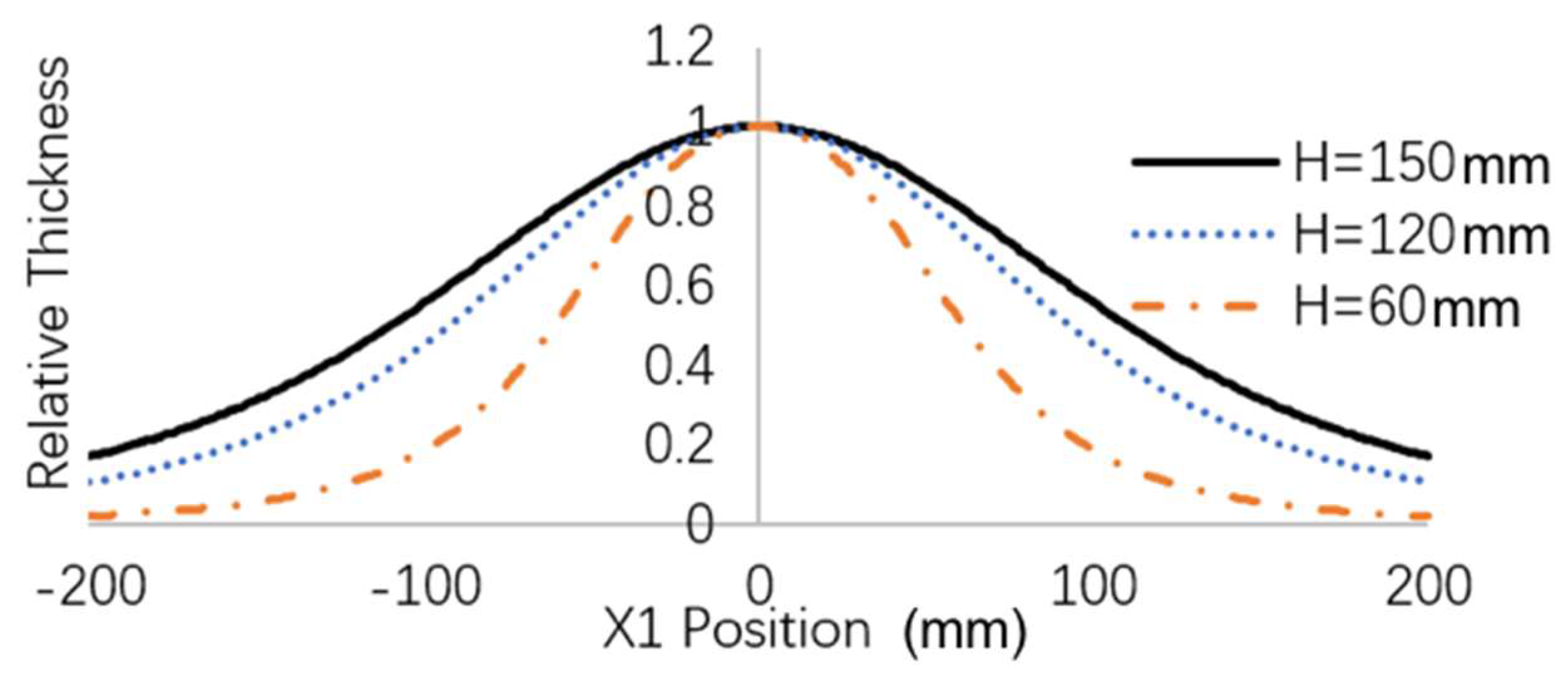
Figure 15 shows that the thickness distribution of the film layer is greatly affected by the distance between the target and the substrate (H), increasing H is found to result in thinner films. The film thickness decreased linearly with H up until 150 mm. After this, the film thickness decreases slowly as H is increased.
As can be seen from Figure 16, when the substrate-target distance (Z, in Figure 14a) is constant, the larger the X1 positions, the thinner the films. When H = 60 mm, as the transverse position becomes larger, the relative film thickness drops sharply. At transverse position X1 = 100 mm, the film thickness has dropped to 18% of the central position, however, for H = 150 mm, the decline rate of the film thickness decreases. At transverse position X1 = 100 mm, the film thickness is 45% of the film thickness in the center position. Therefore, it can be concluded that as the distance from the target to the substrate, H, increases, the film thickness distribution in the transverse direction becomes more uniform, but the deposition rate decreases.
In Figure 17, the Y1 direction distribution uniformity is better than the X1 direction uniformity. As H becomes larger, distribution uniformity in the Y1 direction tends to decrease. However, X1 is less affected. When Y1 is in the range of 0 to 80 mm, the film thickness relative to the center position is more than 80% of the central value. Film thickness in the Y1 direction is relatively uniform, until about 80 mm, and the film thickness does not depend on H as much as for the X1 direction; and this agrees with results from Bo et al. [48].
Based on the above results, it can be found that as the target-substrate distance increases, the film thickness uniformity improves; but the deposition rate decreases significantly and the film uniformity is better along the Y1 direction than the X1 direction.
3.2.2. Rotating Planar Substrate Holder and Circular Sputtering Target
From the above discussions, it is difficult to obtain good uniformity through non-rotating planar substrate holders, and this is often solved by rotating the substrate holder [49].
The parameters for thickness uniformity modelling are shown in Figure 18 and are expressed as:
Bring Equation (46) into Equation (11). Since it is a rotating substrate, integrate α to get the film thickness distribution equation—also, n is assumed to be 1, and is assumed to be 0.
For the effect of the distance between target plane and substrate plane H on film thickness distribution: let D = 20 mm, R1 = 5 mm, and R2 = 20 mm. Then a MathCAD-based program was used to simulate relative thickness distribution of H = 40, 50, 60, 70, 80 mm, from 0 to 50 mm. Figure 19 shows that when D is constant, the film thickness distribution along the ρ direction changes significantly under various H values, higher H values showed better film uniformity. However, as H increases, the film deposition rate decreases. Increasing the H value will also increase the probability of collisions of sputtered atoms with the sputtering gas, that is considered for these calculations. For the effect of D on film thickness distribution: let H = 60 mm, R1 = 5 mm, and R2 = 20 mm, carry out simulation to obtain a relative thickness distribution for D = 0, 20, 40, 60, 80 mm, from 0 to 50 mm.
Figure 20 shows that when H is constant, the film thickness distribution along the ρ direction changes significantly under various D values. Film thickness uniformity has a non-linear relation with D: when D = 0 mm, the relative uniformity error is 25% in the range of the calculated ; when D = 60 mm, the relative uniformity error is 2%, and the uniformity of film thickness is significantly improved. Optimising H and D values can significantly improve film thickness uniformity.
4. Other Factors Affecting Film Thickness Uniformity and Relevant Improvement Methods
4.1. Effect of Tilt of Substrate or Evaporation Source
The tilt of the substrate or the evaporation source is also an important cause of film thickness non-uniformity [50]. If the substrate is tilted, the following equation can be used for correction for small tilt angles (where α is the tilt angle of the substrate):
Taking a planar substrate holder as an example, when α = 0, = 50 mm, the non-uniformity is calculated to be 0.04% for H/L = 1.405 (optimal H/L ratio from Section 3), if the substrate tilt angle is 2°, the non-uniformity increases to 0.6%. Due to improper clamping or thermal deformation, the evaporation source can also be tilted. If the evaporation source is tilted by 5°, the non-uniformity will be 0.3% for a plane substrate holder with = 50 mm, which is more than seven times non-uniformity in the ideal case. Special attention should be made to ensure sources are properly installed for minimization of tilt effects.
4.2. Effect of Vacuum Pressure
The vacuum level is one of the most basic and important parameters in the PVD. Uniformity of film thickness is related to the probability of materials colliding with the residual and process gases in the path to the substrate. For example, in a PVD configuration where H = 760 mm, when the pressure is changed from 0.01 to 0.03 Pa, the optical thickness variation of the center and the edge of the fixture can be increased by 1% for every 10% pressure increase. Therefore, it is possible to improve the film thickness uniformity by reducing the chamber pressure [51].
4.3. Effect of Substrate Temperature
The distribution of substrate temperature in a vacuum chamber is often uneven due to the placements of the heat sources in the vacuum chamber. Typically, the temperature difference between the center and the edges of the fixture can be up to 30 °C [51]. Thus, due to the difference in the condensation, films tend to be thinner at places of higher temperature compared to films at places of lower temperature. Therefore, the temperature field distribution in the vacuum chamber should be controlled appropriately [52].
5. Simulation of Film Thickness Distribution for Evaporation and Sputtering Deposition
In the previous sections, rotation of substrate is shown to improve film uniformity. In actual practice, planetary systems are used (rotating substrate, with orbit and spin) for further improvements of film uniformity. However, the planetary systems are very complex geometrically, and it is not possible to obtain an analytical solution for uniformity calculations. It is also difficult to accommodate very large substrates (e.g., for astronomy applications). The most common method to achieve high film thickness uniformity is to use rotating substrates with masks. Masked deposition is compatible with most equipment configurations and geometries. The main shortcoming of masked depositions is less efficient material utilization [25]. In the literature, mask designs for different substrate holder geometries are proposed [53,54,55,56]. Systems with masks or planetary rotations can only be analyzed for film thickness distribution using simulation.
In this section, a program is written to simulate the thickness distribution of the various systems and validates the above review. The new program can simulate the thickness distribution of all systems discussed in previous sections, and include effects of masks, planetary rotations, and drum-based systems. For the following calculations, the values of n and are determined experimentally, whereas in previous sections, it was assumed that n = 1 and = 0.
5.1. Simulation of Evaporative Deposition
The evaporation source size used in this experiment is relatively small compared to the distance r, thus the source is treated as a small surface source. As shown in the flow chart (Figure 21), the coordinates of any point on the substrate and the coordinates of the source are pre-determined: the coordinates of the source , , ) can be obtained by measurements; coordinates of any point on the substrate (, , ) are a function of time t and angular speed ω.
5.1.1. Rotating Spherical Substrate Holder
The geometry of rotating spherical substrate holder with mask is shown in Figure 22.
where is the angular velocity of the substrate holder, α is the angle of the rotation produced in time t. For these simulations, the following are considered: L = 190 mm, H = 590 mm, R = 660 mm, .
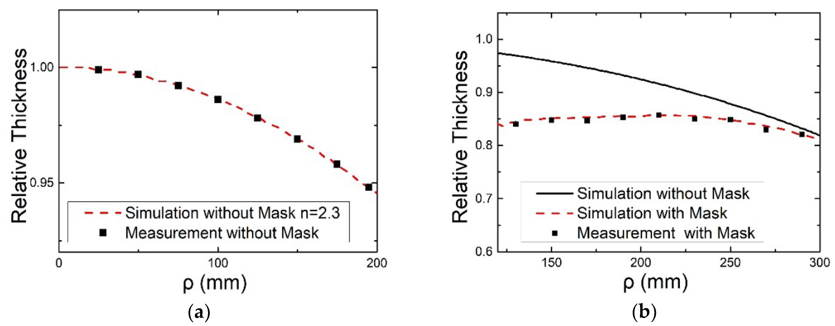
Once (,,) and (,,) are obtained, r, θ, can be obtained. As shown in Figure 23a, the best fit value is n = 2.3. Then the shape of the mask is defined and the final relative film thickness distribution equation is obtained by summing over time (time interval, Δt = 0.0001):
An electron beam deposition system (CVAC700) was used to deposit a layer of H4 (a titanium and antimony compound) on BK7 glass for validating the models. The transmission data for these films were collected using a Perkin Elmer LAMBDA 950 UV/Vis spectrophotometer (Perkin Elmer, Llantrisant, UK) and fitted to obtain thickness of films. The film thickness uniformity was seen to have improved from ±16% to ±0.9% for = 120 to 280 mm after masks were added; and higher uniformity can be achieved with further mask optimization.
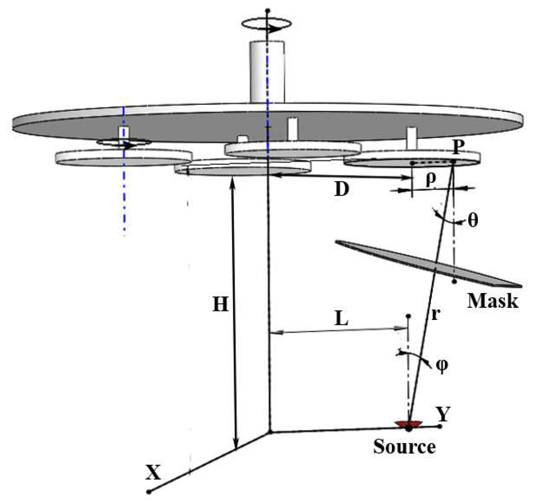
5.1.2. Planetary Substrate Holder
From Figure 24 parameters can be obtained:
is the angular velocity of the main wheel and is the angular velocity of the planetary-wheel. As with the rotating spherical substrate holder, r, θ, are obtained after obtaining the coordinate of the source (, , ) and the coordinate of the points (, , ) on the substrate. If there is no mask, the uniformity error of planetary substrate holder in 0–150 mm range is ±4%. By adding the mask, the film thickness uniformity error was improved from ±4% to ±0.56%, which meets the needs of most high-precision optical film. The calculated results are shown in Figure 25. It can be seen that the film thickness uniformity of the planetary substrate holder is better than the rotating spherical substrate holder, however the complexity of planetary systems limits deposition of ultra-large area optical films. The planetary substrate holders are good for substrates of radius under 200 mm. Also, the masks play a crucial role in optimizing the uniformity of the film thickness.
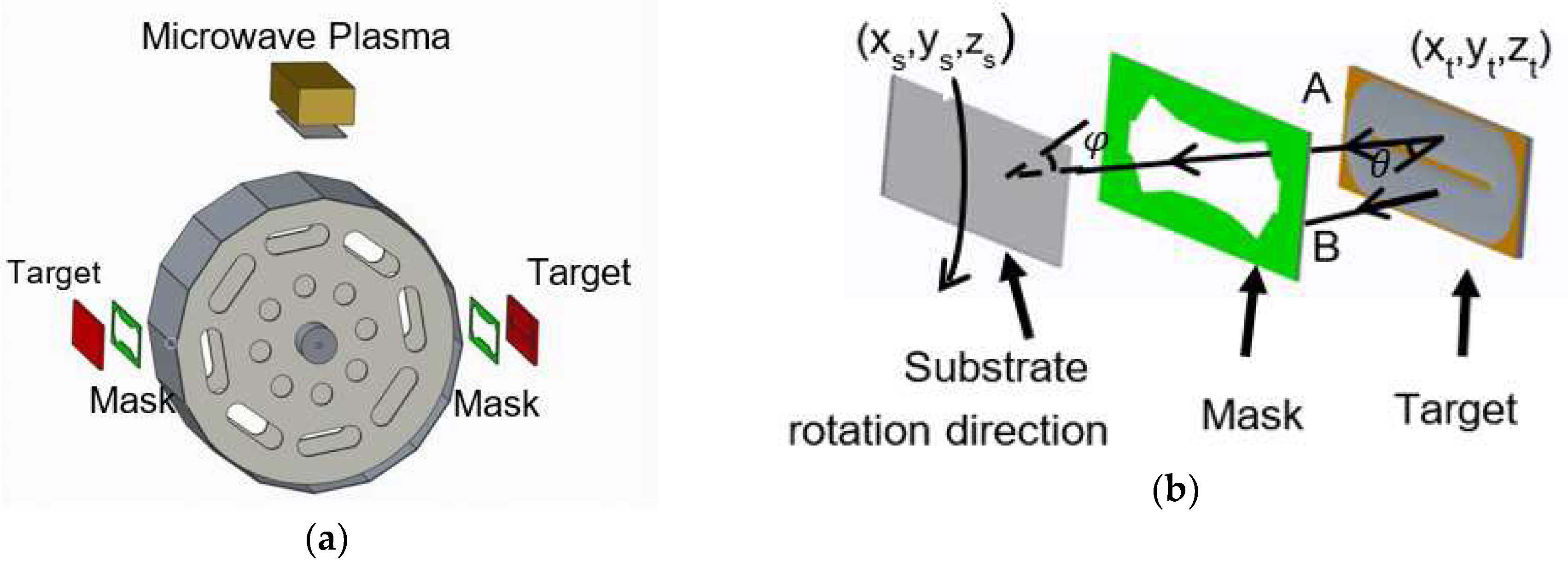
5.2. Simulation of Drum-Based Sputtering Deposition
As shown in the flow chart (Figure 26) the sputtering yield at coordinates of any point () of the target are related to the magnetic field distribution. For convenience, it is obtained by measuring the sputtering erosion track profile of the target, as shown in Figure 27; the details of measurement were given by Li et al. [22]. Due to the rotation of the drum system, the coordinates of any point on the substrate is a function of time and angular speed :
Here, (, , ) are the coordinates on the rotating axis; is the angle of the substrate; R is the radius of the rotating drum. Once () and (, , ) are obtained, r, θ, can be obtained. Trackyield can be defined as the sputtering yield of the target.
Then the shape of the mask is defined, Figure 28b, and the contribution of all points of the target is summed over the range of the substrate rotation angle () to obtain the final film thickness distribution equation. Substrate rotation angle, β, can be considered as the angle between the substrate normal and the target normal.
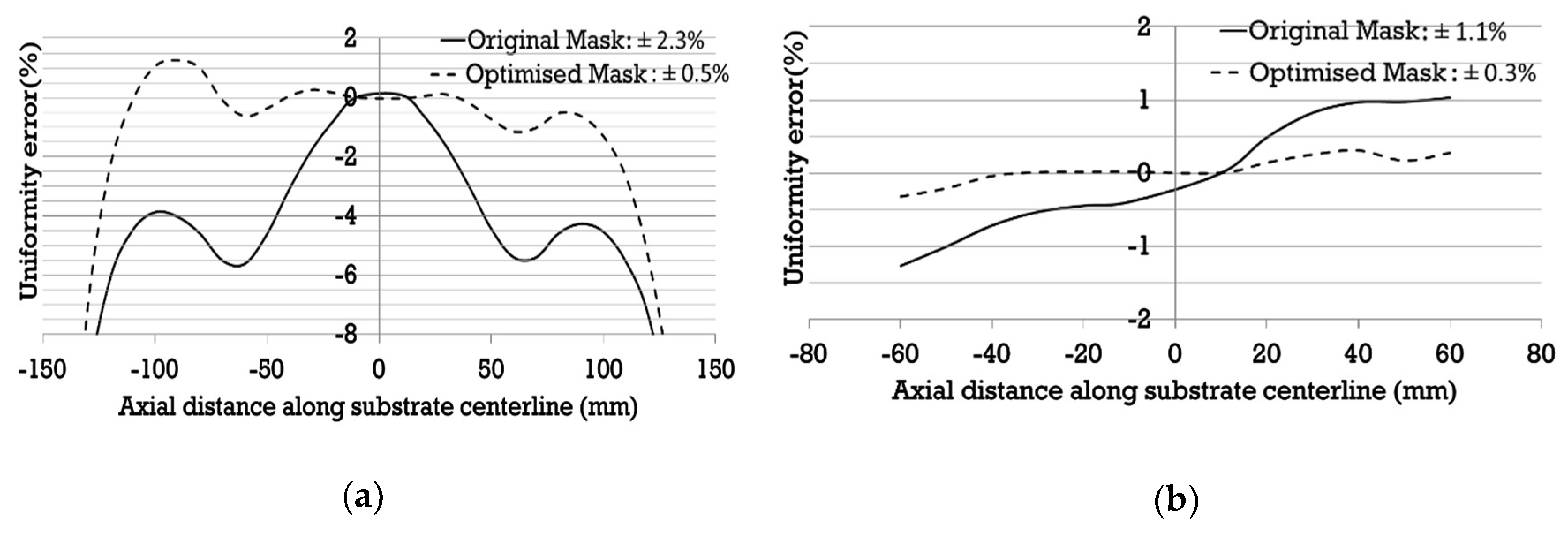
The film thickness distribution with a default mask was obtained through programming simulation ( from 30° to 45°, n from 1 to 10) and shown in Figure 29. It was determined that the best value for the material Nb2O5 is = 37°, n = 5. The uniformity of the film thickness with the default mask was ±2.3%.
Film thickness uniformity can be improved by optimizing the shape of the mask. As shown in Figure 30a, a layer of was deposited on the JGS3 glass substrate using the optimized mask, which reduced the uniformity error from ±2.3% to ±0.5%, as compared to using the original mask. A layer of was deposited on the JGS3 glass substrate using the optimized mask, showing reduced uniformity error from ±1.1% to ±0.3%, as compared to using the original mask. Compared with the previous two sputter models, the rotating drum substrate holder with the correction mask can significantly improve the thickness uniformity of large-area films. Drum-based sputtering system allows deposition of high-precision optical films such as laser protective films and Linear Variable Filter (LVF) [57,58].
6. Conclusions
This paper reviewed the emission characteristics of evaporation and sputtering sources and explored the formulas for emission characteristics of various sources. Film thickness distributions of point, small-surface, extended, and sputtering sources were also reviewed along with relative film thickness distribution and uniformity error for different deposition configurations. These were then simulated with the programs and compared/validated against experimental data. Furthermore, factors that affect the film thickness distribution, such as tilt of substrate or evaporation source, vacuum degree, and uneven substrate temperature were also explored. For complex geometries of deposition systems, such as planetary systems, masked systems, drum-based systems, etc. it was not possible to obtain analytical solutions, and a program was written to model and simulate the relative film thickness distribution using MathCAD. The simulated results demonstrated the improvements to film thickness uniformity gained from using masks and rotating systems. This program will dramatically save process development and optimization time.
Author Contributions
Conceptualization, S.S. and X.F.; Methodology, S.S. and B.W.; Software, S.S. and B.W.; Validation, S.S. and X.F.; Formal Analysis, B.W. and S.S.; Investigation, B.W., S.S., X.F., D.G., Z.W., and Y.S.; Resources, S.S. and D.G.; Data Curation, B.W., C.L., and S.S.; Writing-Original Draft Preparation, B.W., S.S., and H.O.C.; Writing-Review & Editing, B.W. and S.S.; Supervision, S.S. and X.F.
Funding
This research was funded by the Major Scientific and Technological Projects of Jilin Province (20140203002GX).
Conflicts of Interest
The authors declare no conflict of interest.
References
- Van Popta, A.C.; Hawkeye, M.M.; Sit, J.C.; Brett, M.J. Gradient-index narrow-bandpass filter fabricated with glancing-angle deposition. Opt. Lett. 2004, 29, 2545–2547. [Google Scholar] [CrossRef] [PubMed]
- Chu, H.O.; Song, S.; Li, C.; Gibson, D. Surface enhanced raman scattering substrates made by oblique angle deposition: methods and applications. Coatings 2017, 7, 26. [Google Scholar] [CrossRef]
- Darband, G.B.; Aliofkhazraei, M.; Khorsand, S.; Sokhanvar, S.; Kaboli, A. Science and engineering of superhydrophobic surfaces: Review of corrosion resistance, chemical and mechanical stability. Arabian J. Chem. 2018, in press. [Google Scholar] [CrossRef]
- Mattox, D.M. Handbook of Physical Vapor Deposition (PVD) Processing, 2nd ed.; William Andrew: Boston, NY, USA, 2010. [Google Scholar]
- Hill, R.J. Physical Vapor Deposition, 2nd ed.; Temescal a Division of the BOC Group: Berkeley, CA, USA, 1986. [Google Scholar]
- Mahan, J.E. Physical Vapor Deposition of Thin Films, 1st ed.; Wiley-VCH: New York, NY, USA, 2000; p. 336. [Google Scholar]
- Savale, P.A. Physical vapor deposition (PVD) methods for synthesis of thin films: A comparative study. Arch. Appl. Sci. Res. 2016, 8, 1–8. [Google Scholar]
- Kaufman, H.R.; Cuomo, J.J.; Harper, J.M.E. Technology and applications of broad-beam ion sources used in sputtering. Part I. Ion source technology. J. Vac. Sci. Technol. 1982, 21, 725–736. [Google Scholar] [CrossRef]
- Li, P.H.; Chu, P.K. Thin film deposition technologies and processing of biomaterials. In Thin Film Coatings for Biomaterials and Biomedical Applications; Hans, J.G., Ed.; Elsevier: Amsterdam, The Netherlands, 2016; pp. 3–28. [Google Scholar]
- Pinard, L.; Michel, C.; Sassolas, B.; Balzarini, L.; Degallaix, J.; Dolique, V.; Flaminio, R.; Forest, D.; Granata, M.; Lagrange, B.; et al. Mirrors used in the LIGO interferometers for first detection of gravitational waves. Appl. Opt. 2017, 56, C11–C15. [Google Scholar] [CrossRef] [PubMed]
- Raut, H.K.; Ganesh, V.A.; Nair, A.S.; Ramakrishna, S. Anti-reflective coatings: A critical, in-depth review. Energy Environ. Sci. 2011, 4, 3779–3804. [Google Scholar] [CrossRef]
- Madsen, C.K.; Zhao, J.H. Optical Filter Design and Analysis: A Signal Processing Approach, 1st ed.; John wiley & Sons: New York, NY, USA, 1999; pp. 95–154. [Google Scholar]
- Lenner, M.; Fiedler, A.; Spielmann, C. Reliability of laser safety eye wear in the femtosecond regime. Opt. Express 2004, 12, 1329–1334. [Google Scholar] [CrossRef] [PubMed]
- Fancey, K.S. A coating thickness uniformity model for physical vapor-deposition systems: Overview. Surf. Coat. Technol. 1995, 71, 16–29. [Google Scholar] [CrossRef]
- Swann, S.; Collett, S.A.; Scarlett, I.R. Film thickness distribution control with off-axis circular magnetron sources onto rotating substrate holders: Comparison of computer simulation with practical results. J. Vac. Sci. Technol. A 1990, 8, 1299–1303. [Google Scholar] [CrossRef]
- Persad, A.H.; Ward, C.A. Expressions for the evaporation and condensation coefficients in the hertz-knudsen relation. Chem. Rev. 2016, 116, 7727–7767. [Google Scholar] [CrossRef] [PubMed]
- Oliver, J.B.; Talbot, D. Optimization of deposition uniformity for large-aperture National Ignition Facility substrates in a planetary rotation system. Appl. Opt. 2006, 45, 3097–3105. [Google Scholar] [CrossRef] [PubMed]
- Ramprasad, B.S.; Radha, T.S. Uniformity of film thickness on rotating planetary planar substrates. Thin Solid Films 1973, 15, 55–64. [Google Scholar] [CrossRef]
- Usoskin, A.I. Correcting diaphragms for improving the thickness uniformity of vacuum coatings. Sov. J. Opt. Technol. 1984, 51, 471–474. [Google Scholar]
- Guo, C.; Kong, M.; Liu, C.; Li, B. Optimization of thickness uniformity of optical coatings on a conical substrate in a planetary rotation system. Appl. Opt. 2013, 52, B26–B32. [Google Scholar] [CrossRef] [PubMed]
- Kotlikov, E.N.; Prokashev, V.N.; Ivanov, V.A.; Tropin, A.N. Thickness uniformity of films deposited on rotating substrates. J. Opt. Technol. 2009, 76, 100–103. [Google Scholar] [CrossRef]
- Li, C.; Song, S.; Gibson, D.; Child, D.; Waddell, E. Modeling and validation of uniform large-area optical coating deposition on a rotating drum using microwave plasma reactive sputtering. Appl. Opt. 2017, 56, C65–C70. [Google Scholar] [CrossRef] [PubMed]
- Swann, S. Film thickness distribution in magnetron sputtering. Vacuum 1988, 38, 791–794. [Google Scholar] [CrossRef]
- Strijckmans, K.; Depla, D. A time-dependent model for reactive sputter deposition. J. Phys. D Appl. Phys. 2014, 47, 235302. [Google Scholar] [CrossRef]
- Villa, F.; Martínez, A.; Regalado, L.E. Correction masks for thickness uniformity in large-area thin films. Appl. Opt. 2000, 39, 1602–1610. [Google Scholar] [CrossRef] [PubMed]
- Hsu, J.C. Analysis of the thickness uniformity improved by using wire masks for coating optical bandpass filters. Appl. Opt. 2014, 53, 1474–1480. [Google Scholar] [CrossRef] [PubMed]
- Holland, L. Vacuum Deposition of Thin Films, 1st ed.; Chapman & Hall: London, UK, 1970. [Google Scholar]
- Sree Harsha, K.S. Chapter 5: Thermal evaporation source. In Principles of Vapor Deposition of Thin Films, 1st ed.; Elsevier: San Diego, CA, USA, 2005; pp. 367–452. [Google Scholar]
- Depisch, G. Schichtdickengleichmäßigkeit von aufgedampften schichten in theorie und praxis. Vak. Tech. 1981, 3, 67–77. (In German) [Google Scholar]
- Ohring, M. Materials Science of Thin Films: Deposition and Structure, 2nd ed.; Elsevier: San Diego, CA, USA, 2002; pp. 123–125. [Google Scholar]
- Pulker, H.K. Film thickness. In Coatings on Glass, 1st ed.; Elsevier: Amsterdam, The Netherlands, 1999; pp. 318–342. [Google Scholar]
- Balakrishnan, J.; Boyd, I.D.; Braun, D.G. Monte Carlo simulation of vapor transport in physical vapor deposition of titanium. J. Vac. Sci. Technol. A 2000, 18, 907–916. [Google Scholar] [CrossRef]
- Musset, A.; Stevenson, I.C. Thickness distribution of evaporated films. Proc. SPIE 1990, 1270, 287–292. [Google Scholar]
- Sigmund, P. Fundamental Processes in Sputtering of Atoms and Molecules (SPUT92); Kongelige Danske videnskabernes selskab: Copenhagen, Denmark, 1993; p. 675. [Google Scholar]
- Kern, W.; Schuegraf, K.K. Deposition technologies and applications: Introduction and overview. In Handbook of Thin Film Deposition Processes and Techniques, 2nd ed.; Seshan, K., Ed.; Noyes Publications/William Andrew Publishing: Norwich, NY, USA, 2001; pp. 11–43. [Google Scholar]
- Goeckner, M.J.; Goree, J.A.; Sheridan, T.E. Monte Carlo simulation of ions in a magnetron plasma. IEEE Trans. Plasma Sci. 1991, 19, 301–308. [Google Scholar] [CrossRef]
- Bae, K.Y.; Yang, Y.S.; Choi, B.H. Analysis of magnetic field distribution in a cylindrical-type magnetron sputtering system. Proc. Inst. Mech. Eng. B J. Eng. Mach. 2013, 227, 881–889. [Google Scholar] [CrossRef]
- Martynenko, Y.V.; Rogov, A.V.; Shul’ga, V.I. Angular distribution of atoms during the magnetron sputtering of polycrystalline targets. Tech. Phys. 2012, 57, 439–444. [Google Scholar] [CrossRef]
- Villa, F.; Pompa, O. Emission pattern of real vapor sources in high vacuum: An overview. Appl. Opt. 1999, 38, 695–703. [Google Scholar] [CrossRef] [PubMed]
- Huang, Y.X.; Wen, W.Y.; Sun, J.W.; Huai, C.F.; Zeng, H.F.; Zhong, F.H. Thickness uniformity control of sputtered film based on roll-to-roll system with a rectangular target. J. South China Univ. Technol. Sci. 2015, 43, 81–86. (In Chinese) [Google Scholar]
- Fan, Z. Thickness distribution of thin film deposited with magnetro-sputtering. J. Appl. Sci. 1993, 2, 007. [Google Scholar]
- Hu, Z.; Li, Z.; Miao, X.; Liu, W. On the thickness uniformity of films deposited by magnetron sputtering. J. Huazhong Univ. Sci. Technol. 1996, 1, 89–92. (In Chinese) [Google Scholar] [CrossRef]
- Holland, L.; Steckelmacher, W.; Yarwood, J. Vacuum Manual, 1st ed.; Spon: London, UK, 1974; pp. 576–599. [Google Scholar]
- Macleod, H.A. Thin-Film Optical Filters; CRC Press/Taylor & Francis: New York, NY, USA, 2010; pp. 488–509. [Google Scholar]
- Tang, J.F.; Gu, P.F.; Liu, X.; Li, H.F. Modern Optical Thin Film Technology, 2nd ed.; Zhejiang University Press: Hangzhou, China, 2006; pp. 24–31. (In Chinese) [Google Scholar]
- Gu, P.F. Theoretical calculation of thickness uniformity of optical thin films. Laser Infrared 1985, 1, 47–50. (In Chinese) [Google Scholar]
- Willke, B.; Aufmuth, P.; Aulbert, C.; Babak, S. The GEO 600 gravitational wave detector. Classical Quantum Gravity 2002, 19, 1377. [Google Scholar] [CrossRef]
- Yang, B. Study On the Distribution of Magnetic Filed and Thin Film Thickness Uniformity of Magnetron Sputterings System. Master’s Thesis, Xi’an University of Technology, Xi’an, China, 2009. (In Chinese). [Google Scholar]
- Ma, H.C. Uniformity Analysis of Substrate Film Thickness of Magnetron Sputtering Machine. Master’s Thesis, Northeastern University, Shenyang, China, 2010. (In Chinese). [Google Scholar]
- Oliver, J.B. Analysis of a planetary-rotation system for evaporated optical coatings. Appl. Opt. 2016, 55, 8550–8555. [Google Scholar] [CrossRef] [PubMed]
- Dong, H.K.; Zhao, J.H.; Lin, R.L.; Hu, N.X.; Chen, C.G. Study and analysis on the film uniformity. Piezoelectr. Acoustoopt. 2006, 28, 578–580. [Google Scholar]
- Tian, M.B.; Liu, D.L. Chapter 3: Optical properties of thin films. In Handbook of Thin Film Science and Technology, 1st ed.; Mechanical Industry Press: Beijing, China, 1991; pp. 131–156. (In Chinese) [Google Scholar]
- Arkwright, J.; Underhill, I.; Pereira, N.; Gross, M. Deterministic control of thin film thickness in physical vapor deposition systems using a multi-aperture mask. Opt. Express 2005, 13, 2731–2741. [Google Scholar] [CrossRef] [PubMed]
- Liu, C.; Kong, M.; Guo, C.; Gao, W.; Li, B. Theoretical design of shadowing masks for uniform coatings on spherical substrates in planetary rotation systems. Opt. Express 2012, 20, 23790–23797. [Google Scholar] [CrossRef] [PubMed]
- Abzalova, G.I.; Sabirov, R.S.; Mikhailov, A.V. Depositing uniform-thickness coatings on large surfaces by means of electron-beam evaporation in vacuum. J. Opt. Technol. 2005, 72, 799–801. [Google Scholar] [CrossRef]
- Grezes-Besset, C.; Richier, R.; Pelletier, E. Layer uniformity obtained by vacuum evaporation: Application to Fabry-Perot filters. Appl. Opt. 1989, 28, 2960–2964. [Google Scholar] [CrossRef] [PubMed]
- Gottmann, J.; Kreutz, E.W. Pulsed laser deposition of alumina and zirconia thin films on polymers and glass as optical and protective coatings. Surf. Coat. Technol. 1999, 116, 1189–1194. [Google Scholar] [CrossRef]
- Ko, C.H.; Chang, K.Y.; Huang, Y.M. Analytical modeling and tolerance analysis of a linear variable filter for spectral order sorting. Opt. Express 2015, 23, 5102–5116. [Google Scholar] [CrossRef] [PubMed]
Figure 1.
Theoretical leaf-shaped vapor clouds for different cosine exponents calculated using MathCAD.
Figure 1.
Theoretical leaf-shaped vapor clouds for different cosine exponents calculated using MathCAD.

Figure 2.
Schematic diagram of virtual evaporation source with regions of viscous flow and molecular flow; h is the height of substrate to the real source surface; hv is the height of substrate to the center of the virtual source.
Figure 2.
Schematic diagram of virtual evaporation source with regions of viscous flow and molecular flow; h is the height of substrate to the real source surface; hv is the height of substrate to the center of the virtual source.
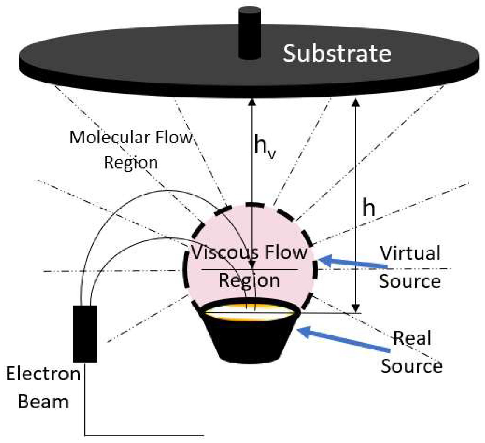
Figure 3.
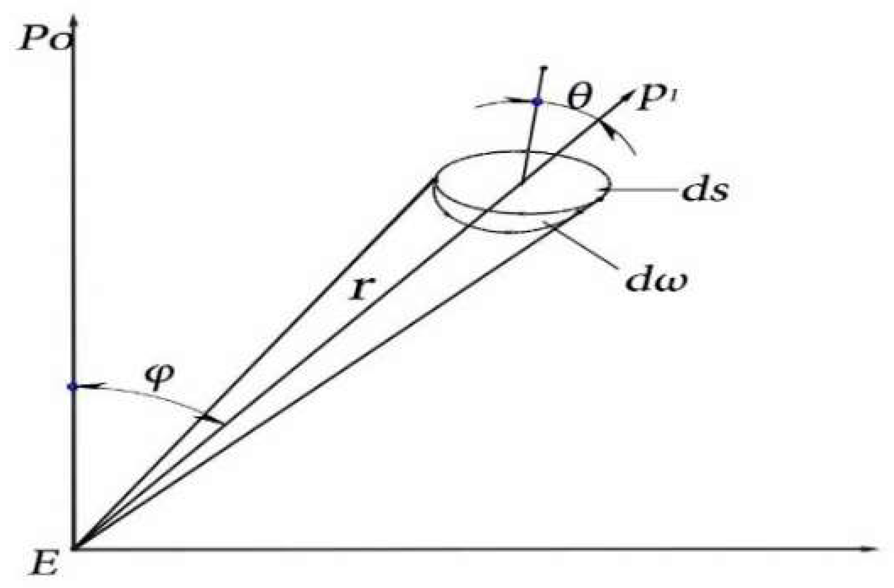
Influence of angle on thickness of film. Where ds is the substrate element, d is the solid angle, r is the evaporation distance. is the angle between the source normal and the line connecting the evaporation source to the substrate element, is the angle between the surface normal of the film and the line connecting the evaporation source to the substrate element, E is the evaporation source.
Figure 3.
Influence of angle on thickness of film. Where ds is the substrate element, d is the solid angle, r is the evaporation distance. is the angle between the source normal and the line connecting the evaporation source to the substrate element, is the angle between the surface normal of the film and the line connecting the evaporation source to the substrate element, E is the evaporation source.

Figure 4.
(a) Molybdenum boats for thermal evaporation; (b) crucible for electron-beam (EB) evaporation.
Figure 4.
(a) Molybdenum boats for thermal evaporation; (b) crucible for electron-beam (EB) evaporation.
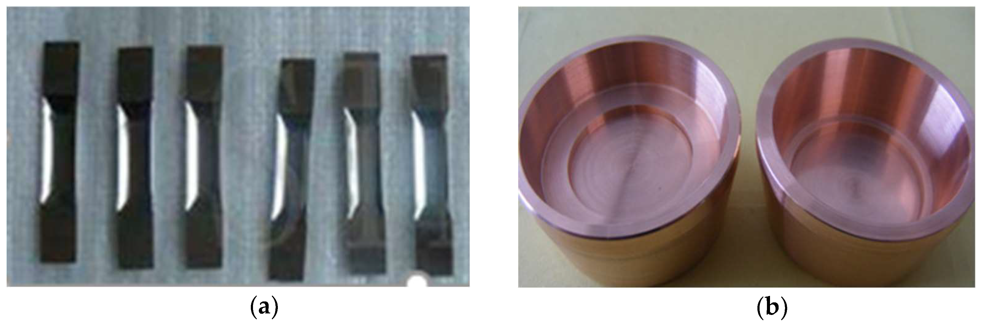
Figure 5.
(a) Racetrack shape in rectangular sputtering target; (b) racetrack in circle shaped target.
Figure 5.
(a) Racetrack shape in rectangular sputtering target; (b) racetrack in circle shaped target.
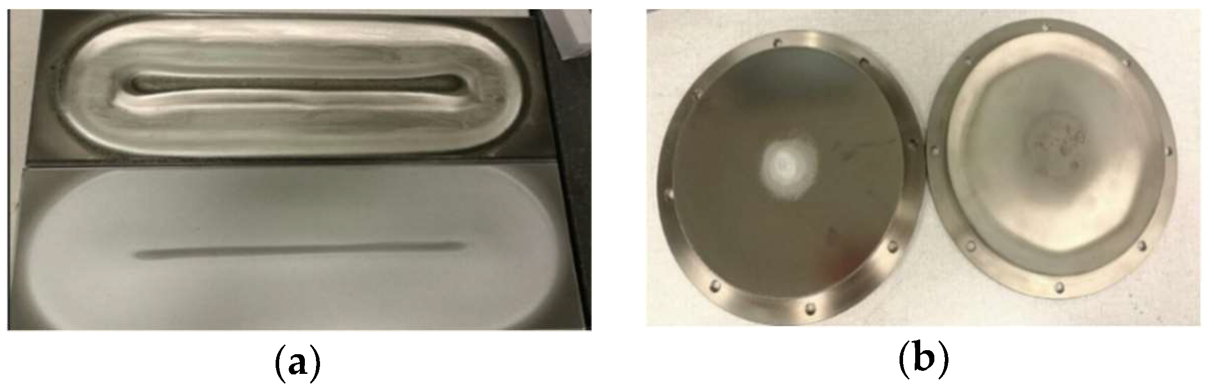
Figure 6.
Flat plate substrate holder, where H is the distance between the source and the substrate holder; is the angle between the normal of the source and the line connecting the source and the P point; θ is the angle between the normal of the substrate and the line connecting the source and the P point; is the distance from the center of the substrate holder to the P point; r is the distance from the source to the P point; P is any point on the substrate holder.

Figure 7.
Distribution of the thin film thickness on the flat plate substrate holder in relation to position/height ratio.
Figure 7.
Distribution of the thin film thickness on the flat plate substrate holder in relation to position/height ratio.
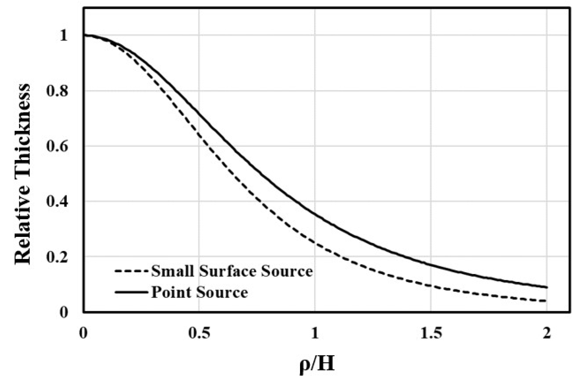
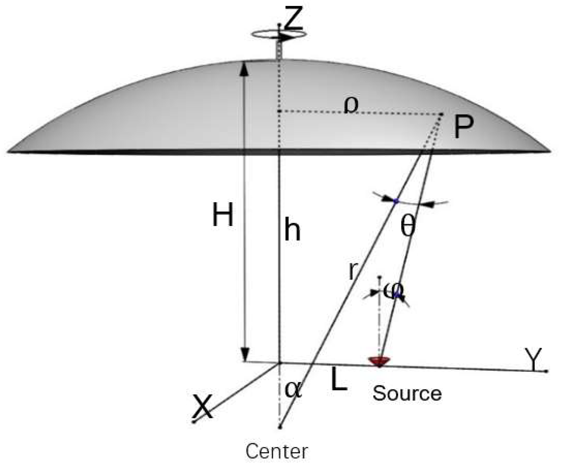
Figure 8.
Spherical surface substrate holder, where H is the distance between the source and the top of the substrate holder, h is the height of sample to the source position, is the angle between the normal of the source and the line connecting the source to the P point; is the angle between the normal of the substrate and the line connecting the source to the P point; is the distance from the center of the substrate holder to the P point; r is the distance from the source to the P point; P is any point on the substrate holder. R is the diameter of the spherical dome.

Figure 9.
Distribution of the thin film thickness on the spherical surface substrate holder.
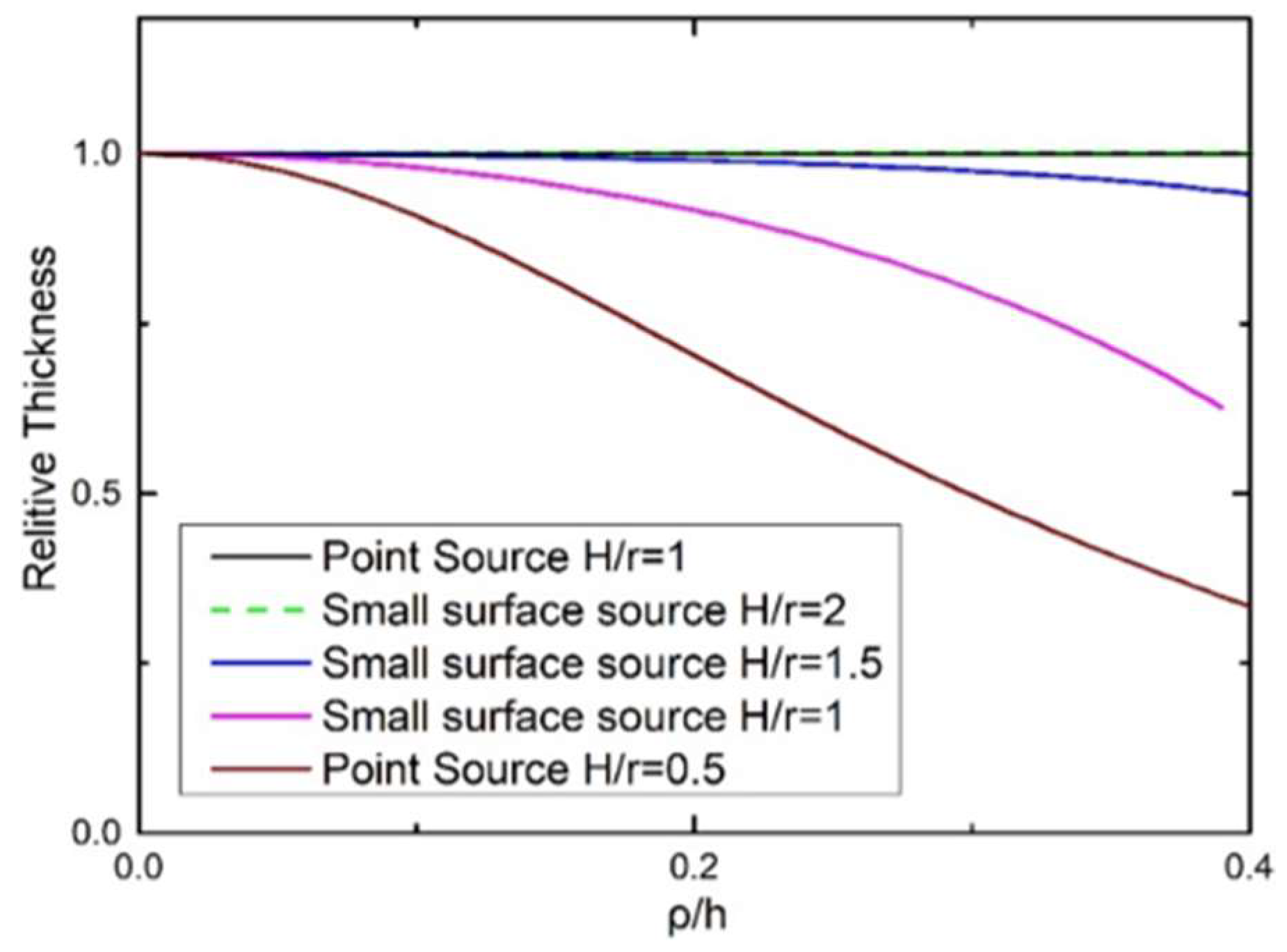
Figure 10.
Rotating planar substrate holder, where H is the distance between the source and the substrate holder; is the angle between the normal of the source and the line connecting the source to the P point; is the angle between the normal of the substrate and the line connecting the source to the P point; is the distance from the center of the substrate holder to the P point; r is the distance from the source to the P point; L is the distance from the source to the center; P is any point on the substrate holder.
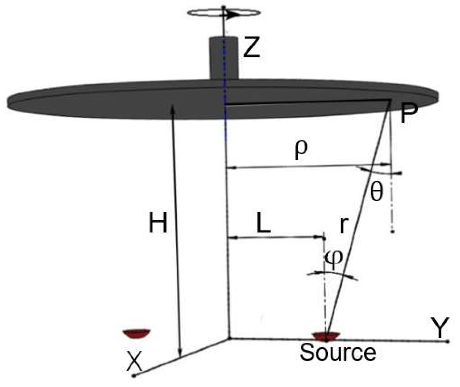
Figure 11.
(a) Distribution of the thin film thickness on the rotating planar plate substrate holder; (b) Distribution for optimized H/L values, to demonstrate finer details for better comparison.
Figure 11.
(a) Distribution of the thin film thickness on the rotating planar plate substrate holder; (b) Distribution for optimized H/L values, to demonstrate finer details for better comparison.
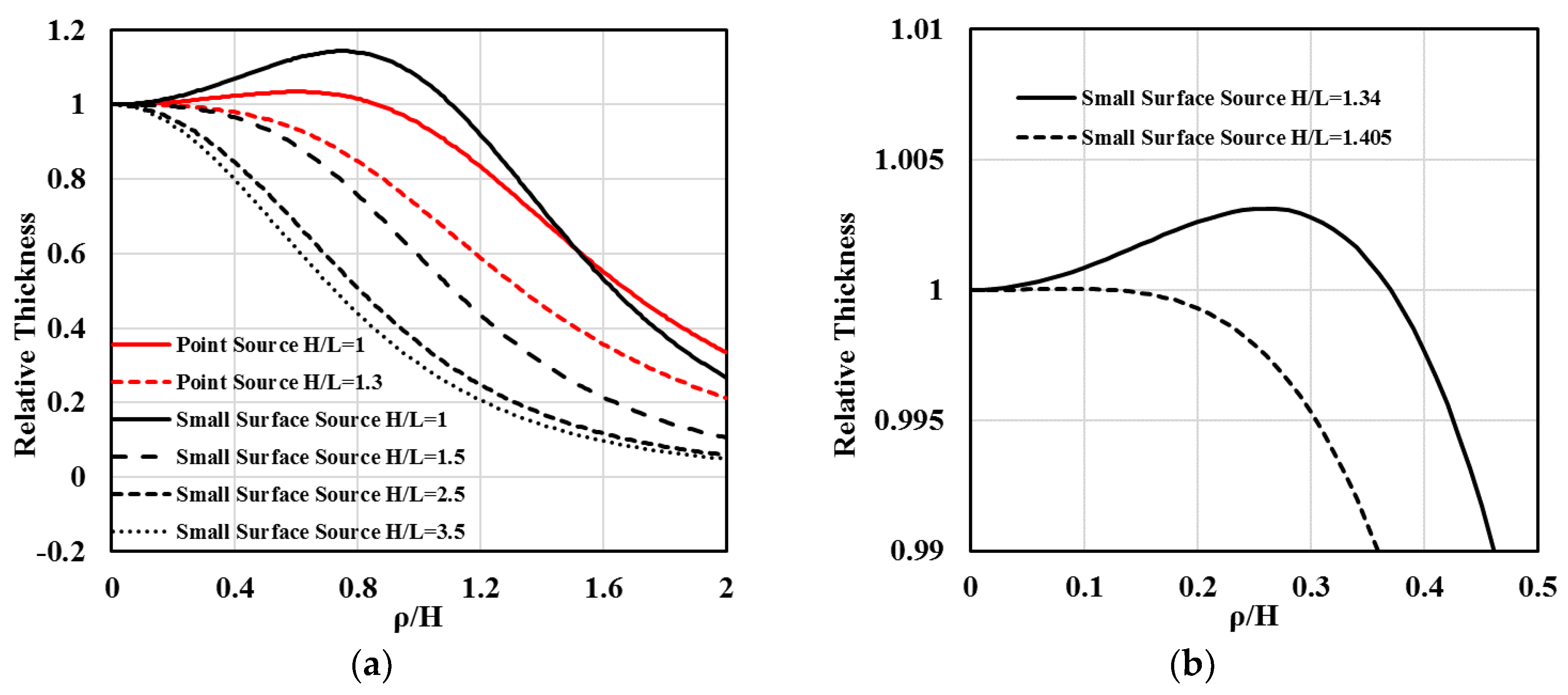
Figure 12.
Rotating spherical substrate holder, where H is the distance between the source and the top of the substrate holder, h is the height of sample to the source position, is the angle between the normal of the source and the line connecting the source to the P point; is the angle between the normal of the substrate and the line connecting the source to the P point; is the distance from the center of the substrate holder to the P point; r is the distance from the source to the P point; L is the distance from the source to the center; P is any point on the substrate holder.

Figure 13.
Distribution of the thin film thickness for small-surface sources on the rotating spherical surface substrate holder.
Figure 13.
Distribution of the thin film thickness for small-surface sources on the rotating spherical surface substrate holder.

Figure 14.
(a) Planar substrate holder with rectangular sputtering target, where H is the distance between the target plane and the substrate holder plane, is the angle between the normal of the target and the line connecting the point to the point; is the angle between the normal of the substrate and the line connecting the point to the point; r is the distance the point to the point; is any point on the substrate holder; is any point on the target; (b) 2D projection of the target. The track area, labelled as q(x, y), that is treated as the sputtering/target area.

Figure 15.
Relative film thickness distribution at different heights.

Figure 16.
Relative film thickness distribution at X1 positions, as described in Figure 14.
Figure 16.
Relative film thickness distribution at X1 positions, as described in Figure 14.

Figure 17.
Relative film thickness distribution at different Y1 positions.
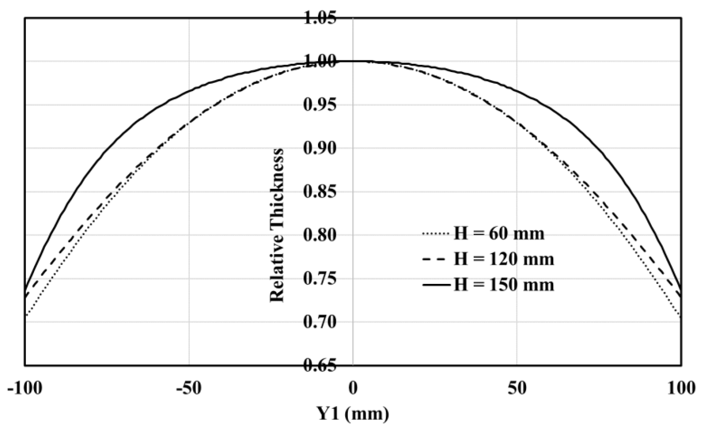
Figure 18.
(a) Rotating planar substrate holder and circular sputtering target, where H is the distance between the target plane and the substrate holder plane, is the angle between the normal of the target and the line connecting the point to the point; is the angle between the normal of the substrate and the line connecting the point to the point; r is the distance from the point to the point; is the distance from the point to the center of the substrate; D is the horizontal distance from the target center to the substrate holder center; is any point on the substrate holder; is any point on the target; (b) 2D projection of target, where is the inner ring radius; is the outer ring radius; and R is the distance from the point to the center of the target.
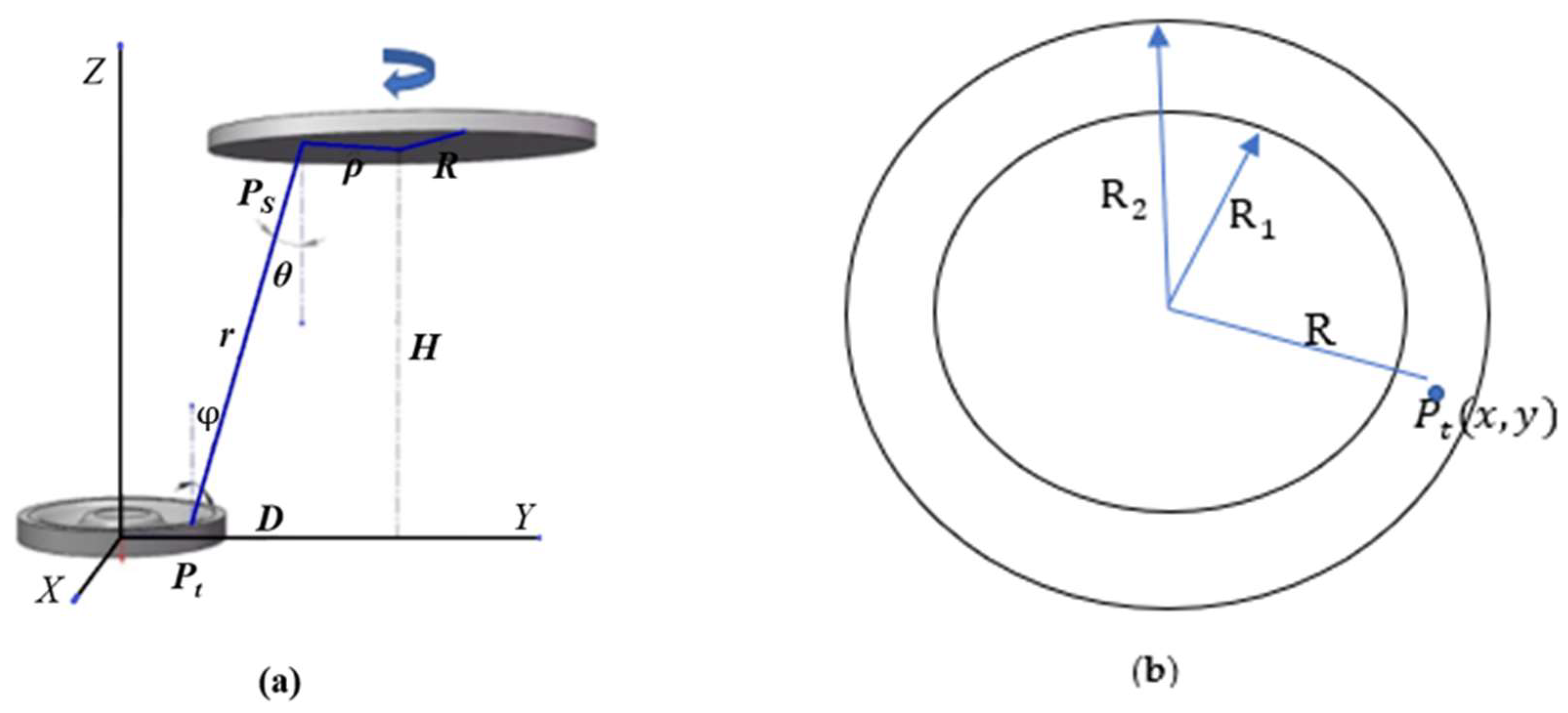
Figure 19.
Relative film thickness distribution of H = 40, 50, 60, 70, 80 mm, from 0 to 50 mm.
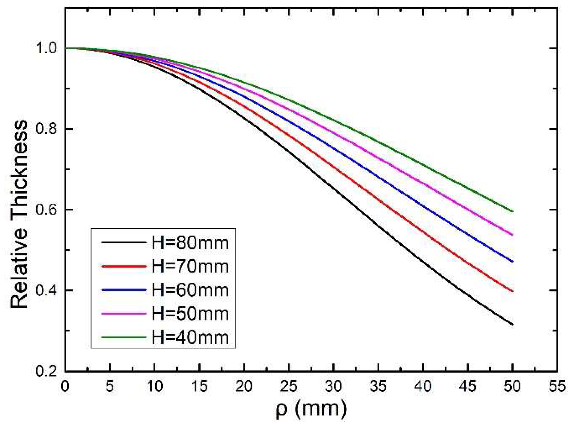
Figure 20.
Relative film thickness distribution of D = 0, 20, 40, 60, 80 mm, from 0 to 50 mm.
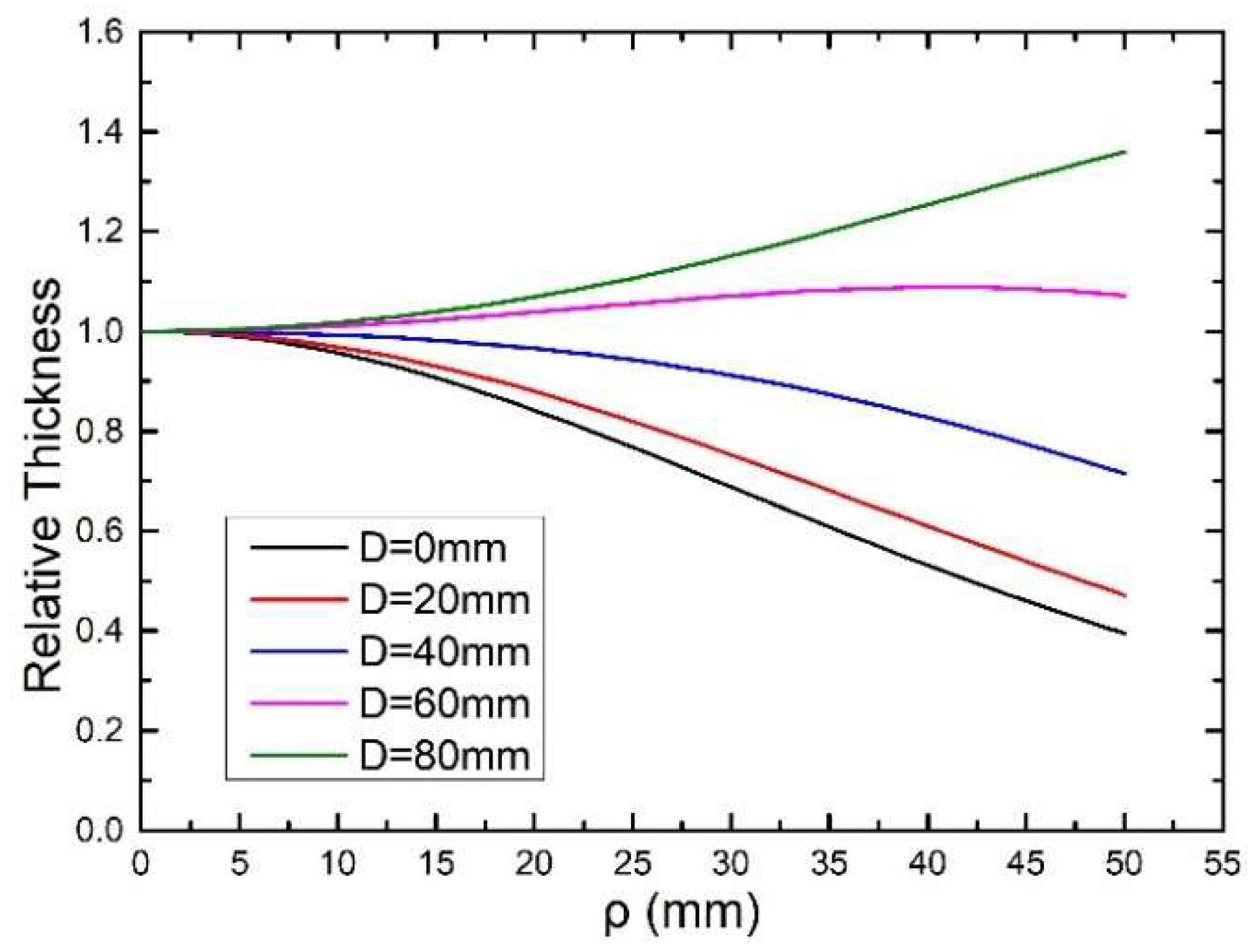
Figure 21.
The evaporation flow chart of the simulation on thickness distribution; passrate is a binary, 0 or 1, describing whether the evaporation material reaches the substrate or if it is blocked by the mask.
Figure 21.
The evaporation flow chart of the simulation on thickness distribution; passrate is a binary, 0 or 1, describing whether the evaporation material reaches the substrate or if it is blocked by the mask.
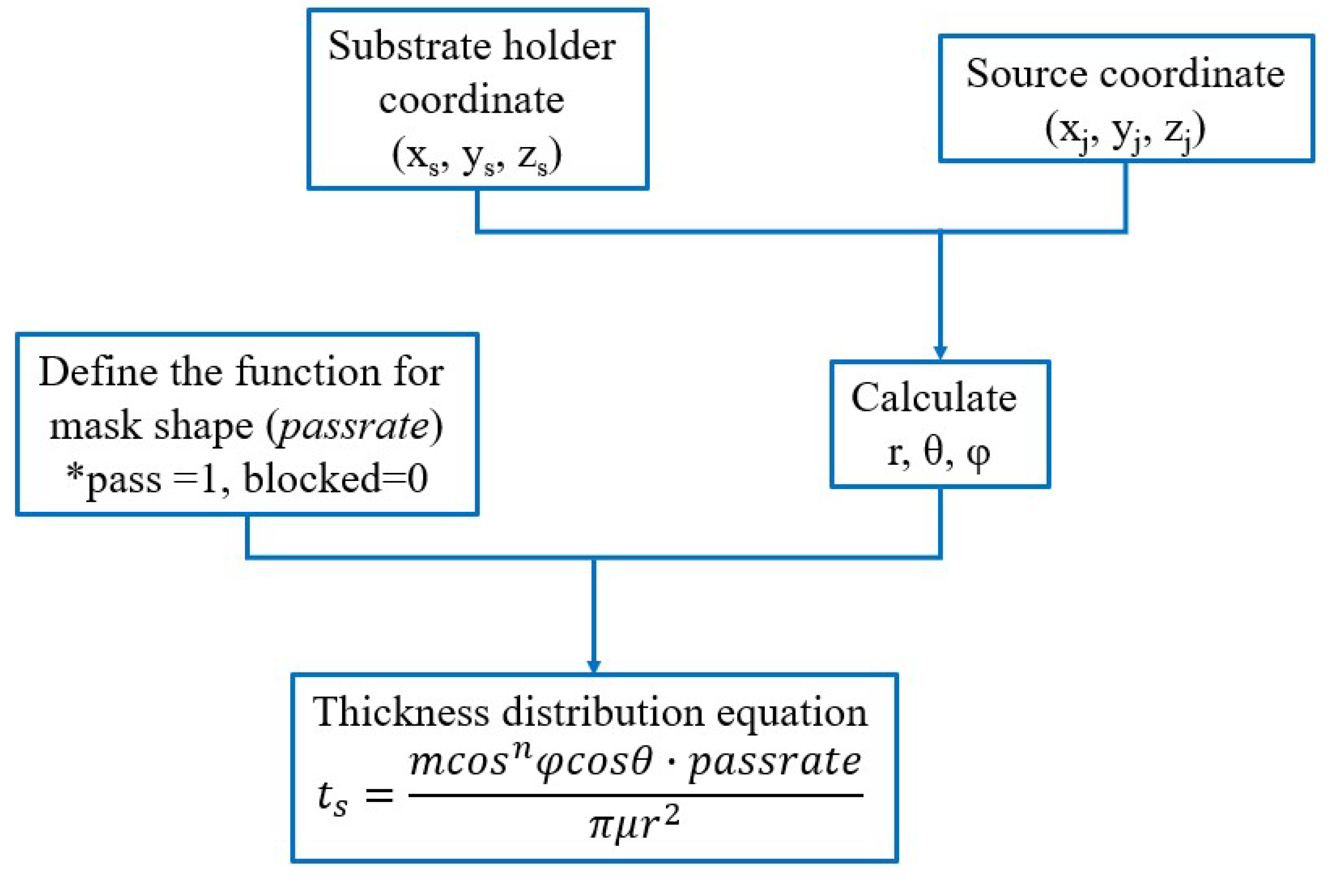
Figure 22.
Rotating spherical substrate holder with mask, where H is the distance between the source and the top of the substrate holder; h is the height of the sample to the source position; is the angle between the normal of the source and the line connecting the source to the P point; is the angle between the normal of the substrate and the line connecting the source to the P point; is the distance from the center of the substrate holder to the P point; r is the distance from the source to the P point; L is the distance from the source to the center; P is any point on the substrate holder; R is the diameter of the spherical dome.

Figure 23.
(a) The simulated depositions and measurement are used to obtain values of n, without mask; (b) The thickness distribution of simulation and measurement, the samples are placed from = 120 and above due to the position of the rotation axis and the crystal controller.
Figure 23.
(a) The simulated depositions and measurement are used to obtain values of n, without mask; (b) The thickness distribution of simulation and measurement, the samples are placed from = 120 and above due to the position of the rotation axis and the crystal controller.

Figure 24.
Planetary substrate holder with mask, where H is the distance between the source and the top of the substrate holder; is the angle between the normal of the source and the line connecting the source to the P point; is the angle between the normal of the substrate and the line connecting the source to the P point; is the distance from the center of the substrate holder to the P point; r is the distance from the source to the P point; L is the distance from the source to the center; D is the distance from the main axis to the planetary axis; and P is any point on the substrate holder, (L = 400 mm, H = 830 mm, D = 310 mm, , ).

Figure 25.
(a) The thickness distribution simulation with and without mask; (b) shape of the mask.
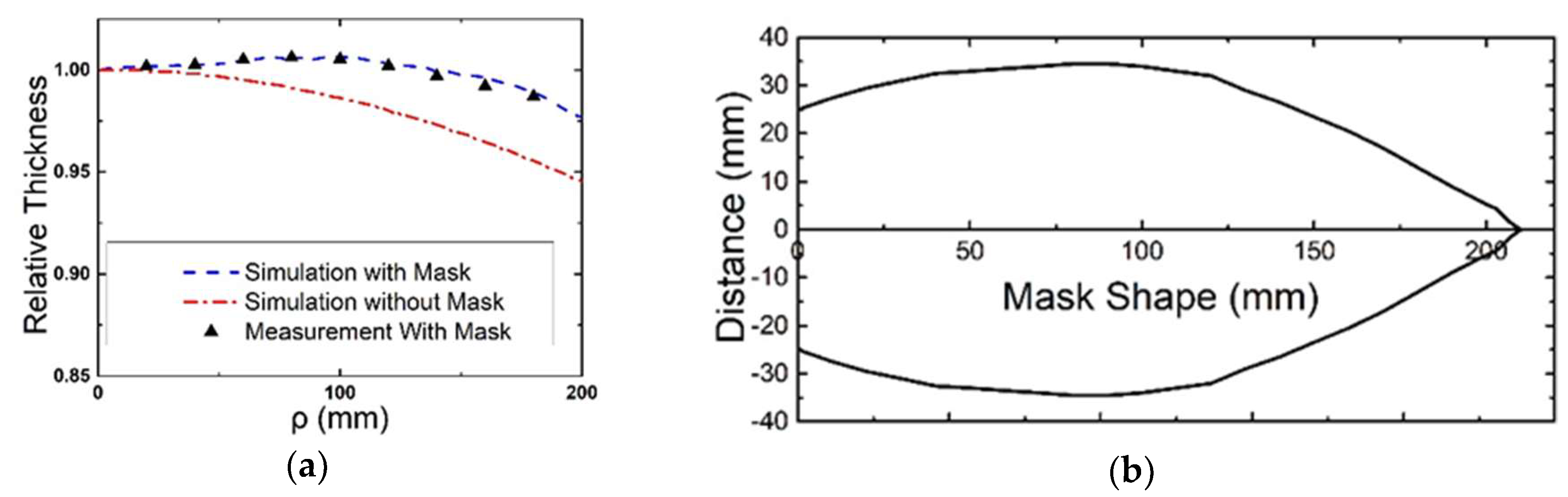
Figure 26.
Flow chart for simulation of thickness distribution from sputtering deposition; is a binary, 0 or 1; trackyield is the sputtering yield of the target.
Figure 26.
Flow chart for simulation of thickness distribution from sputtering deposition; is a binary, 0 or 1; trackyield is the sputtering yield of the target.
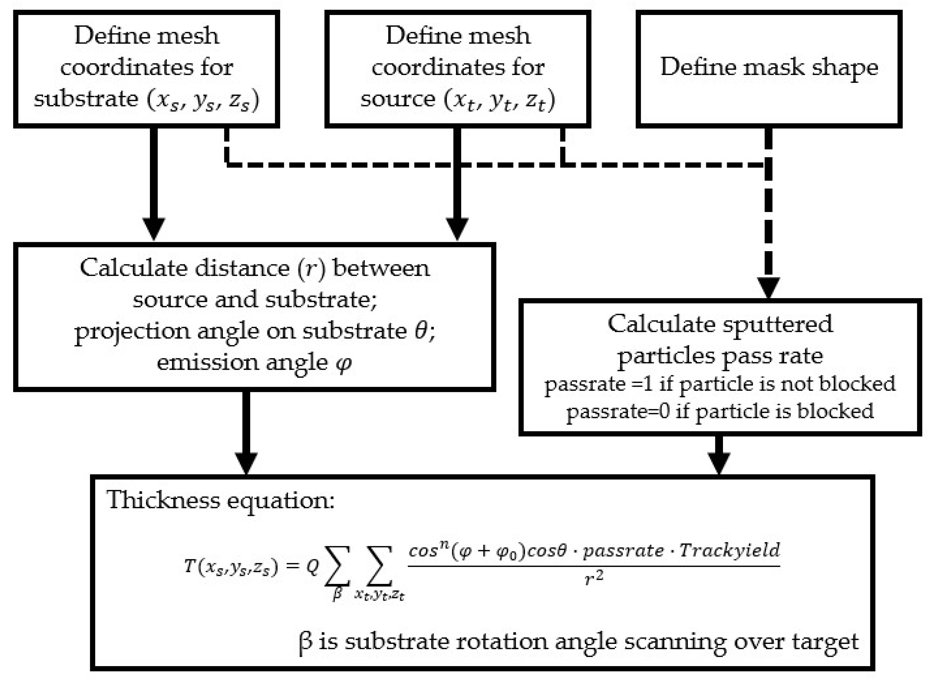
Figure 27.
The sputtering erosion track of the target (trackyield).
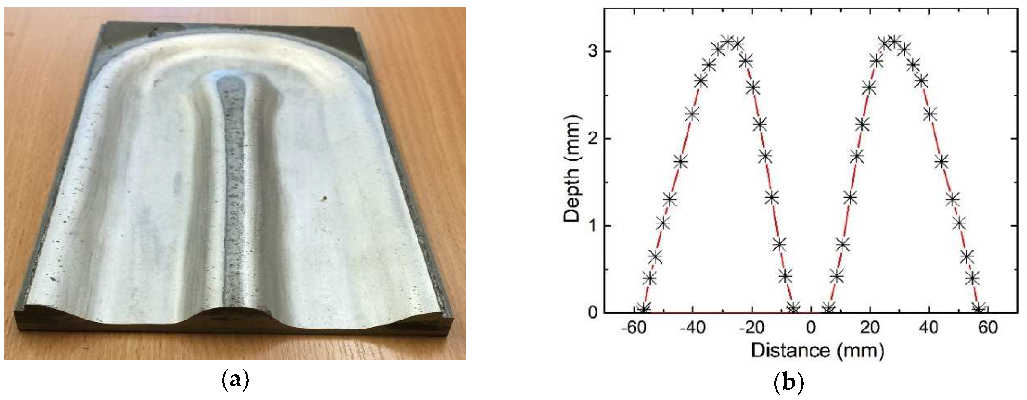
Figure 28.
(a) Rotating drum substrate holder. (b) is the emission angle to the target surface of ejected sputter flux; is the incident angle to the substrate surface of deposited atom flux; path A: direct line of sight from target to substrate; path B: mask blocked sputter flux.
Figure 28.
(a) Rotating drum substrate holder. (b) is the emission angle to the target surface of ejected sputter flux; is the incident angle to the substrate surface of deposited atom flux; path A: direct line of sight from target to substrate; path B: mask blocked sputter flux.

Figure 29.
(a) Simulated uniformity distribution and measured uniformity distribution, n and 0 are obtained by fitting measured data with the original mask shape, the mask shape was then optimized using these parameters; (b) Original mask shape and optimized mask shape.
Figure 29.
(a) Simulated uniformity distribution and measured uniformity distribution, n and 0 are obtained by fitting measured data with the original mask shape, the mask shape was then optimized using these parameters; (b) Original mask shape and optimized mask shape.
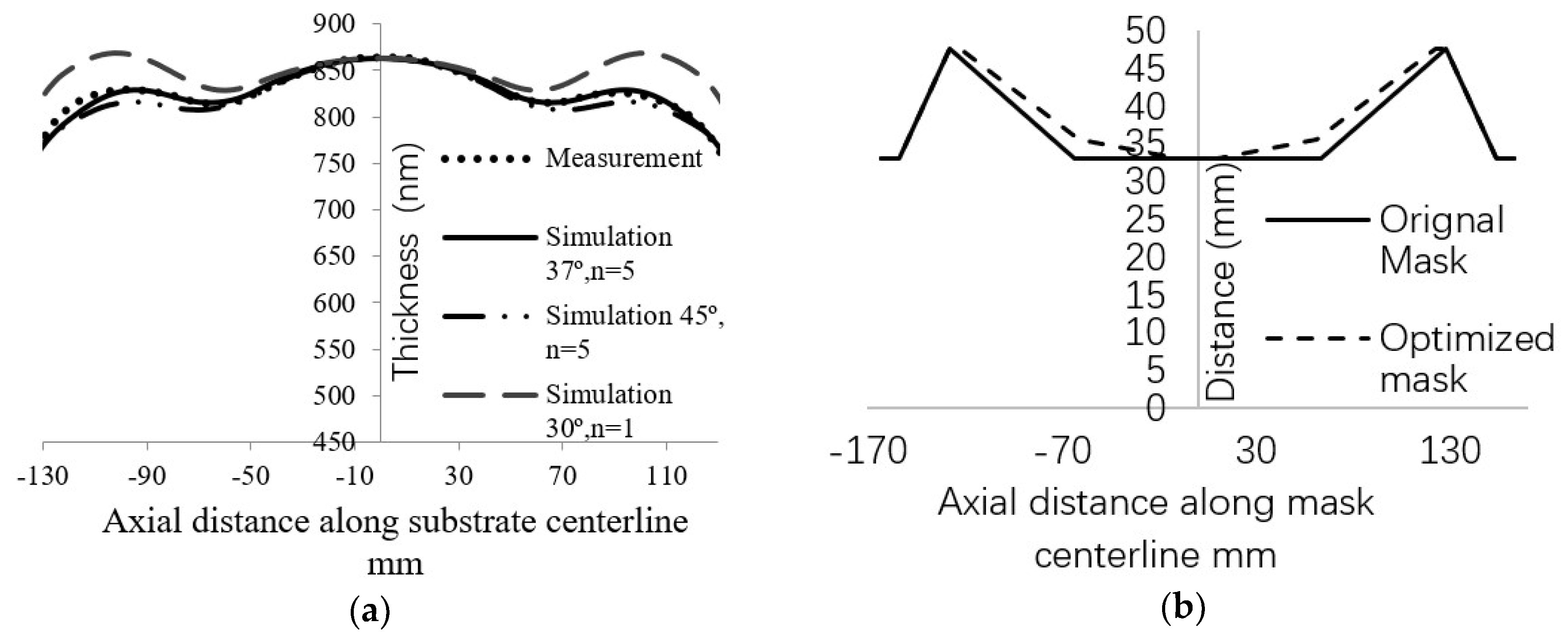
Figure 30.
Coating uniformity of (a) Nb2O5 film and (b) SiO2 film.


Table 1.
Summary for emission characteristics of the source.
| Source Type | Ideal Point Source | Small Surface Source (Approximated Point Source) | Extended Source | Sputter Source |
|---|---|---|---|---|
| Emission characteristics | uniformly emitted vapor molecules in all directions | or | or | . or |
Table 2.
Thin film thickness distributions for different types of sources.
| Source Types | Thickness Distribution | |
|---|---|---|
| Evaporation source | Point source | |
| Small surface source | ||
| Extended Source | ||
| Sputtering source | ||
© 2018 by the authors. Licensee MDPI, Basel, Switzerland. This article is an open access article distributed under the terms and conditions of the Creative Commons Attribution (CC BY) license (http://creativecommons.org/licenses/by/4.0/).
Share and Cite
MDPI and ACS Style
Wang, B.; Fu, X.; Song, S.; Chu, H.O.; Gibson, D.; Li, C.; Shi, Y.; Wu, Z. Simulation and Optimization of Film Thickness Uniformity in Physical Vapor Deposition. Coatings 2018, 8, 325. https://doi.org/10.3390/coatings8090325
AMA Style
Wang B, Fu X, Song S, Chu HO, Gibson D, Li C, Shi Y, Wu Z. Simulation and Optimization of Film Thickness Uniformity in Physical Vapor Deposition. Coatings. 2018; 8(9):325. https://doi.org/10.3390/coatings8090325
Chicago/Turabian StyleWang, Ben, Xiuhua Fu, Shigeng Song, Hin On Chu, Desmond Gibson, Cheng Li, Yongjing Shi, and Zhentao Wu. 2018. "Simulation and Optimization of Film Thickness Uniformity in Physical Vapor Deposition" Coatings 8, no. 9: 325. https://doi.org/10.3390/coatings8090325
Note that from the first issue of 2016, this journal uses article numbers instead of page numbers. See further details here.