1. Introduction
The increasing degree of global industrialisation and high demand for fossil fuel is becoming a serious issue in gas emissions contributing to greenhouse effect terms. High efficiency renewable energy sources are a need in an ever-more energy demanding world. Concentrated solar power plants have proven to be a real clean alternative for energy harvesting. Nowadays, the largest concentrated solar power (CSP) plant, Ivanpah in USA, has an installed power of 390 MW [
1]. A total production of 5 GW was reached worldwide in 2017 by means of CSP plants which, translated into energy, represents 0.2% of the total energetic demand of electric energy [
2]. Despite these numbers, efficiencies and costs of solar plants, or so-called levelized costs of energy, are still a “needs to improve” factor. Its technology is relatively novel compared with well-established competitors and consequently, there is still a large gap for improvement.
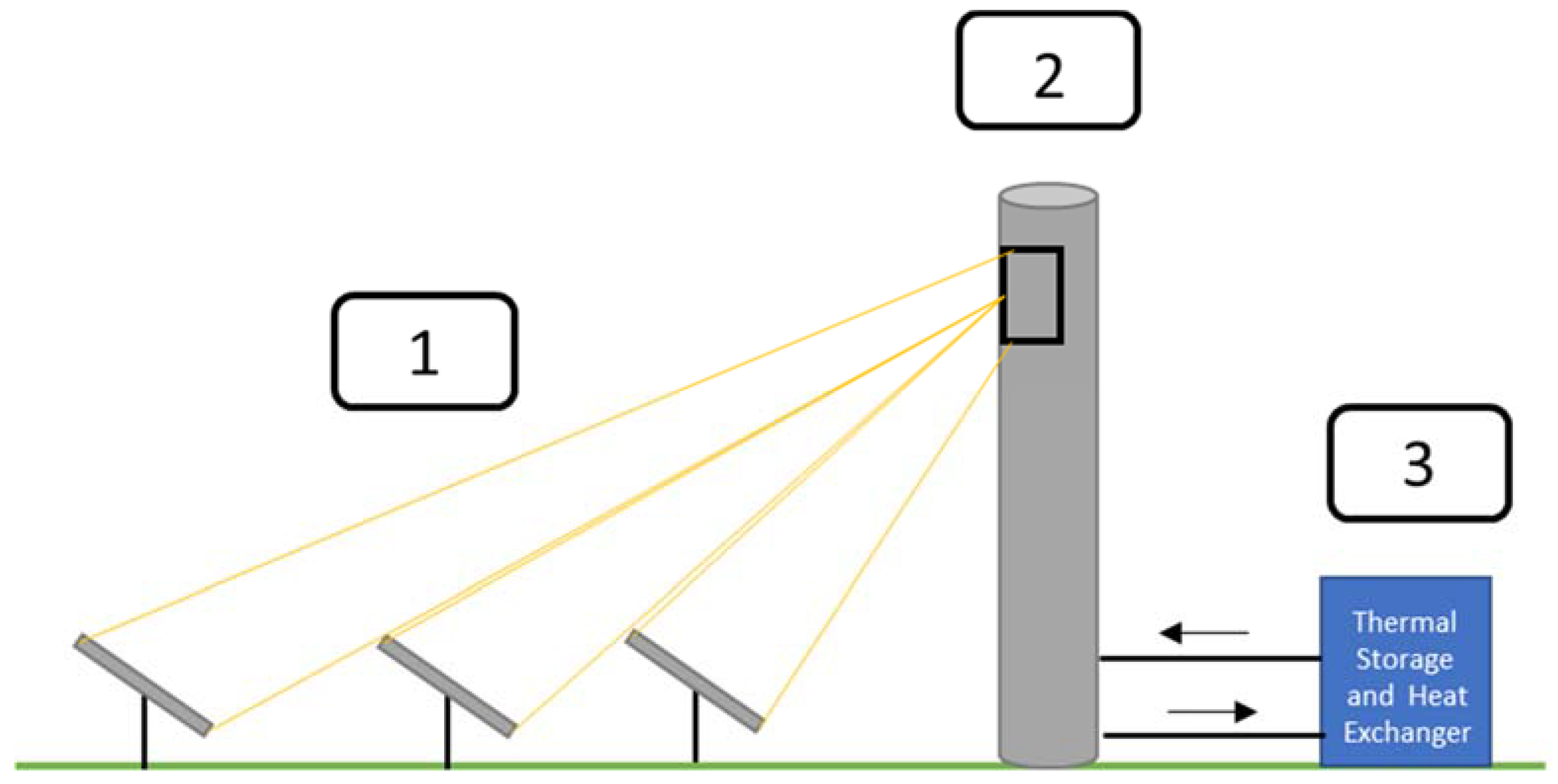
There are different types of CSP plants depending on the configuration of collectors and receivers. Parabolic dish, parabolic trough collectors, linear Fresnel collectors, and central tower systems [
3] are the most commonly used ones and all of them have mainly the same operation schemes. Mirrors (solar collectors) concentrate solar radiation towards solar receivers, thereby increasing the temperature of a heat transfer fluid. Thermal energy is moved downstream by the heat transfer fluid and is converted into electricity by a heat exchanger and a steam turbine in a power generator.
Surface science and engineering solutions (in particular, thin film and plasma technologies) have been found to provide improvements to CSP plants by tackling at least three different key components: high reflecting thin film solar collectors, solar selective coatings [
4] in the receivers, and anti-corrosion layers for protecting thermal storage tanks [
5] (see
Figure 1).
Most of the CSP plants utilise second face mirrors fabricated by means of wet chemistry processes [
6]. The reflectivity (solar weighted reflectivity) of commercial CSP ranges from 84 to 95%. The highest reflectivity is achieved using silver as reflecting element [
7]. Other commercial solutions with lower reflectance (<90%) include aluminium and silvered polymer layers as reflecting materials [
8]. However, main suppliers worldwide are investing in the development of dry fabrication processes such as physical vapour deposition (PVD) based technologies. PVD could bring improvements in optical properties and stability towards atmospheric inclemency. The increase in mirror specular reflectance (even at a few percentage points level) could significantly reduce the number of heliostats needed to reach the same temperatures at the solar receiver, bringing down the plant construction and operating expenses [
9]. In this regard, the implementation of high energy PVD techniques such as filtered cathodic vacuum arc (FCVA) could yield high density reflecting thin films with improved reflectance and better environmental stability. The high density of the films achieved using FCVA, because of the high energy at which particles reach the substrate, was the main reason for choosing this technique among others. This density can improve corrosion resistance by reducing grain boundaries and surface roughness.
In addition, improvements could also be achieved by modifying the manufacturing process. Nowadays, reflecting metals are chemically deposited in the back of extra clear glass in such a way that reflecting metals are atmosphere protected (second face mirror configuration), but partially scarifying the specular reflectance [
10]. In first face mirrors, the reflecting material is deposited directly on top of the glass. However, the metal surfaces studied degraded rapidly due to weathering (i.e., rain or sand storms) and cleaning processes, causing a substantial decrease in the reflectance, thus making them unsuitable for solar thermal first face applications [
11,
12]. The development of atmosphere stable highly reflective coatings would open the possibility of the usage of cheaper substrates such as standard glass. This would dramatically decrease the solar plant costs as the extra clear glass holds approximately 60% of the final price of the CSP mirror [
13,
14].
This study is aimed to achieve higher specular reflecting mirror surfaces to improve the yield of CSP solar plants. The studied first surface mirror concept is investigated as an alternative to well-established second surface mirror approaches, currently focusing on the reduction of the extra clear glass thickness on top of silver. Thereby, absorption-induced losses by the protective glass are prevented. In general, aluminium is a material presenting less durability issues than silver that is mainly used in state-of-the-art second surface mirrors. It is less prone to tarnishing than silver and it has a better mechanical performance. Moreover, aluminium forms an environmentally stable and hard natural oxide that could prevent or at least slow down mirror degradation. Finally, the Al/AlOx mirror concept has no internal interfaces that could undergo material failure. For that purpose, a series of aluminium thin films was deposited using FCVA at different working pressures and deposition times. The achieved optical performance of the films was studied depending on their structural properties. Rutherford backscattering spectrometry (RBS) was applied to explore the potential oxidation of the films during deposition or post-deposition air exposure. Surface morphological changes were explored by scanning electron microscopy (SEM). In addition, atomic force microscopy (AFM) measurements at different deposition times allowed exploring the dynamics of the growth mechanism of the films.
2. Materials and Methods
A set of aluminium thin films was deposited on glass slides and silicon (100) wafers using a 90° pulsed FCVA equipment (Plasma Technologies, Kowloon, Hong Kong) [
15]. Substrates were previously ultrasonicated for 10 min in (a) 0.5% Hellmanex solution in water, (b) acetone, and (c) ethanol. Before metal deposition, substrates were precleaned in the vacuum chamber with a flow of argon (60 sccm) applying a DC bias of 750 V (80% duty cycle) at 1.5 Pa for 15 min. Truncated cones (
Φ1 = 65 mm,
Φ2 = 50 mm, and height = 35 mm) made of aluminium (99.99%) were used as metallic targets for the depositions. The process was carried out applying a DC current of 20 A at an argon flow of 20 sccm without bias current. The processes were performed at different pressures (0.1, 0.25, 0.5, and 1 Pa) by controlling a throttle valve and at different deposition times (2, 5, 10, and 20 min). An additional sample deposited at 0.1 Pa for one min was prepared in order to study by AFM the early stages of film growth. A summary of deposition parameters is shown in
Table 1.
Film thickness and roughness were measured using a mechanical profilometer DektakXT (Bruker, Billerica, MA, USA) from Bruker. It was equipped with a 4 μm diameter diamond tipped stylus that applied 3 mg force for these measurements. Root mean square roughness (
Ra) was calculated according to the standard ISO4287-1997 [
16].
Reflectance was measured using a Lambda 1050 spectrophotometer (Perkin Elmer, Waltham, MA, USA). The system was equipped with a deuterium and a tungsten halogen lamps covering the wavelength ranges of 175–320 nm and 320–3300 nm, respectively. An integrating sphere (150 mm diameter) coated with Spectralon and the universal reflectance accessory (URA) were used to measure total and absolute specular reflectance, respectively. The integrating sphere has a photomultiplier tube (PMT) and InGaAs detectors and the URA accessory uses silicon and PbS detectors for the ultraviolet-visible (UV-vis) and near-infrared (NIR) region of the spectra, respectively. A calibrated silver mirror was used as reflectance reference.
For solar weighted reflectance (SWR) calculations, total and specular spectral reflectance
RT,S(λ) were measured in a spectral range between 300 nm and 2500 nm. SWR was obtained by calculating a weighted average using a referenced solar spectral irradiance (
G(λ), ASTM G173-03 AM 1.5), as defined in ISO 9050 [
17]:
Scanning electron microscopy (SEM) was performed for microstructure characterisation of the samples using a S5200 SEM (Hitachi, Tokyo, Japan) equipped with a field emission gun (FEG). Aluminium conducting samples were measured from top and cross-sectional views at 1–5 kV electron beam energy.
Rutherford backscattering spectrometry (RBS) was measured on samples deposited on silicon substrate in Helmholtz–Zentrum Dresden–Rossendorf (HZDR) in Dresden, Germany using a 2 MeV Van der Graaff accelerator by using
4He
+ ions with an energy of 1.7 MeV. The data were acquired using a silicon barrier detector located at a backscattering angle of 170°, whose energy resolution was 13 keV. SIMNRA software was used for simulation of the layer’s areal density and atomic composition [
18].
Atomic force microscopy (AFM) images were measured using a NTEGRA Spectra II (NTMDT Spectrum instruments, Moscow, Russia) using a non-contact mode. Sample areas of 10 μm × 10 μm were measured using NSG01 tips from NTMDT.
3. Results and Discussion
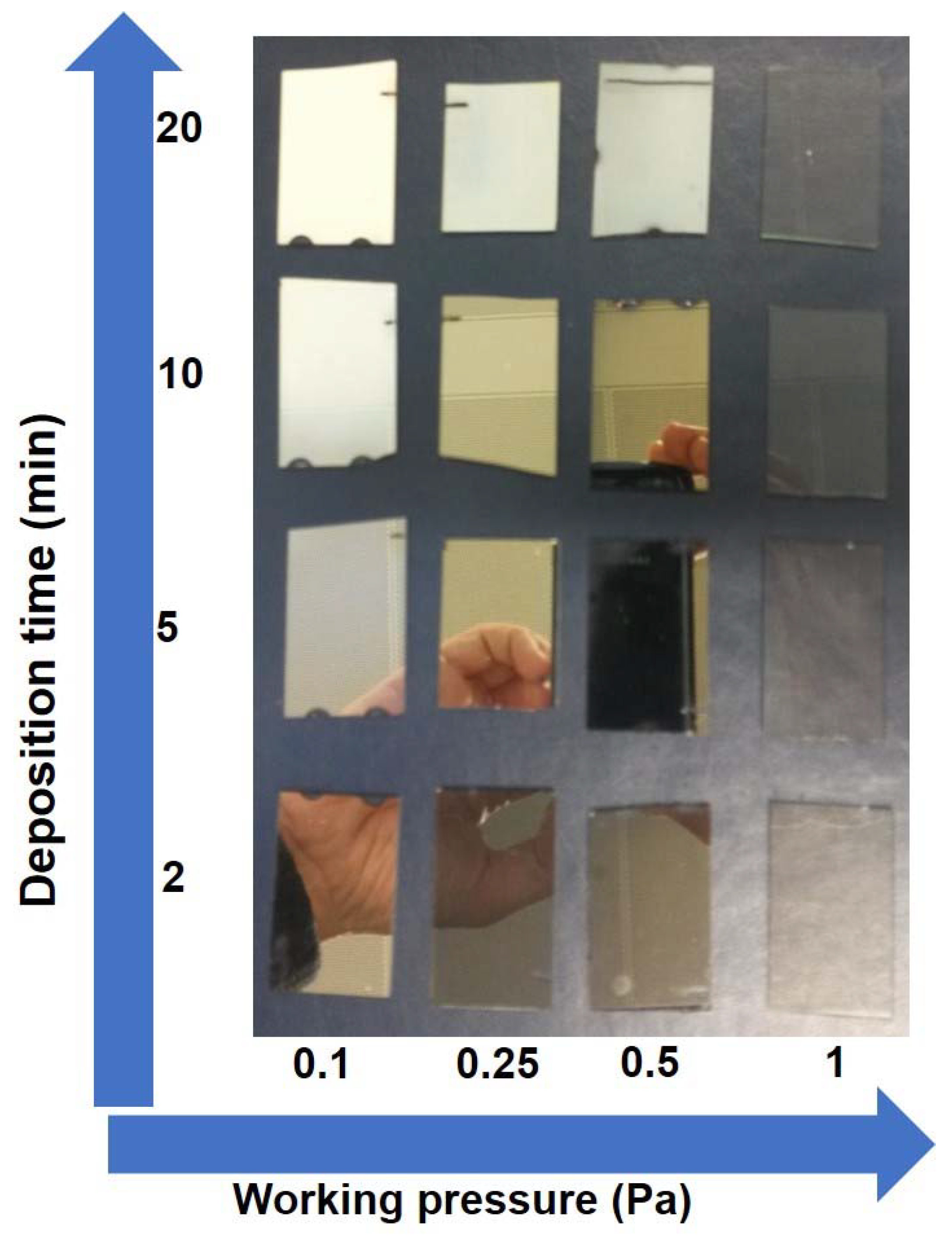
The series of aluminium thin layers deposited using FCVA at different working pressures (
Pw) (0.1, 0.25, 0.5, and 1 Pa) and during different deposition times (2, 5, 10, 20 min) shows distinct differences in their visual appearance and reflectivity (
Figure 2). At first glance, a low working pressure and short deposition times lead to highly reflective, higher working pressures and long deposition times to transparent films, respectively.
Table 2 shows the deposition rates of the films as a function of the working pressure calculated from the slope of the plot of the film thickness measured from profilometry versus the deposition time. A drastic decrease of the deposition rate with the working pressure is observed, and it varies from 27 nm/min for samples deposited at 0.1 Pa down to less than 2 nm/min for those prepared at 1 Pa. It is known that in PVD processes, the working pressure affects the mean free path of particles in the plasma [
19,
20]. In short, at high working pressures, the collision probability of the impinging particles is high and subsequently, fewer particles with lower energies are able to reach the substrate surface, which results in lower deposition rates. Contrarily, at low pressures, the mean free path of the particles increases and a high density of energetic particles reach the substrate surface. Hence, all samples deposited at the highest working pressure are transparent or semi-transparent due to their low thickness (<10 nm for the longest deposition time of 20 min). Samples prepared under intermediate working pressures (0.5 and 0.25 Pa) showed an evolution from semi-transparent to opaque appearance and only those samples deposited at the lowest pressure of 0.1 Pa were found to be non-transparent within the complete time range under study. As stated in the introduction, the main objective of the work was the optimization of aluminium thin films for reflecting surfaces. Therefore, the detailed morphological, compositional, and optical study described below is focused on the series of samples deposited at 0.1 Pa as a function of the deposition time, which exhibits the best reflective properties according to the visual inspection.
Samples ranging in thickness from 23 to 548 nm, as measured by profilometry, were obtained (see
Table 3). The elemental concentration depth profile of the set of samples prepared at
Pw = 0.1 Pa (
t = 2–20 min) was obtained by RBS measurements.
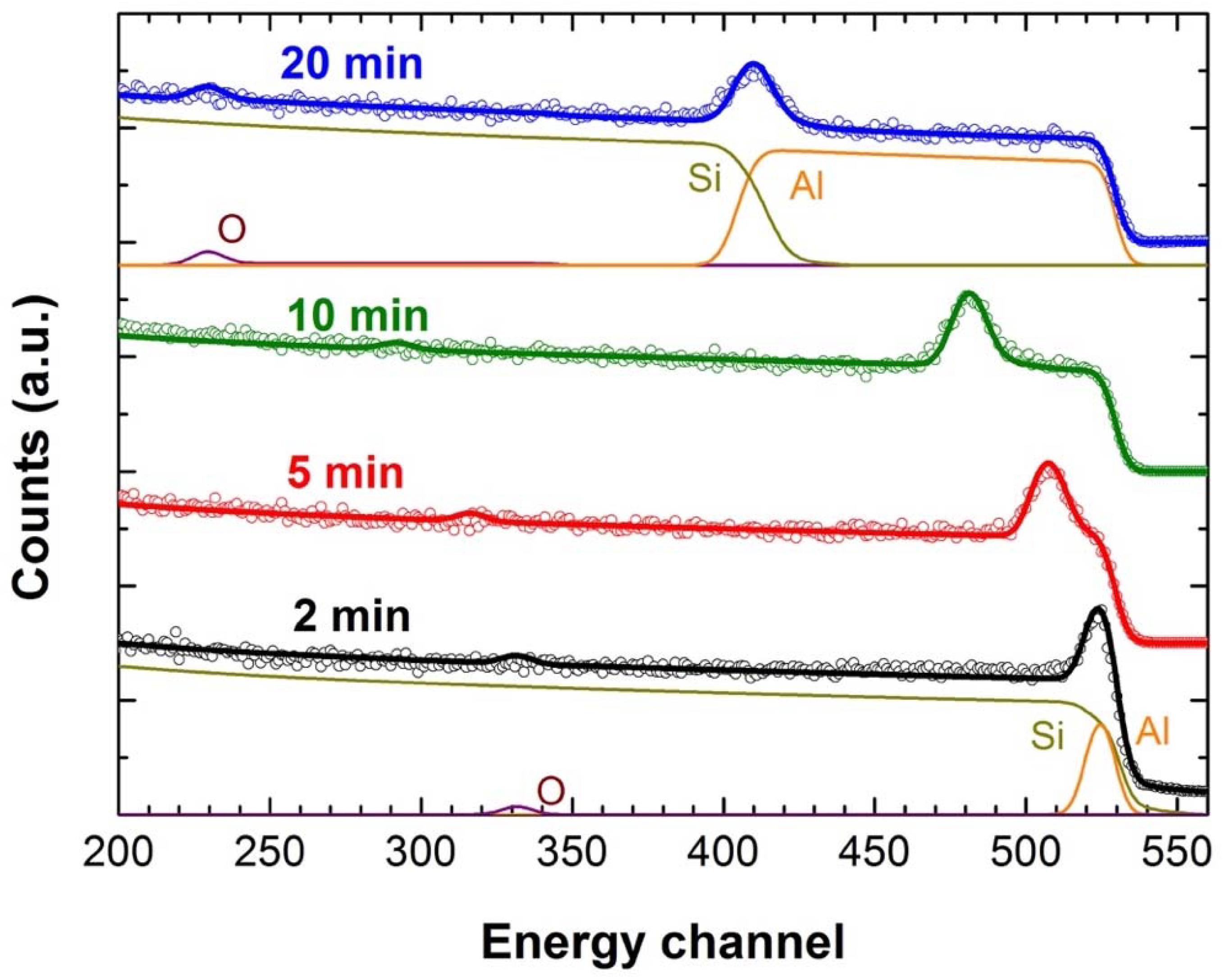
Figure 3 shows the RBS spectra of the samples together with their corresponding fit as obtained by SIMNRA. The deconvolution of the RBS spectrum in their individual element components is shown for the samples deposited for 2 and 20 min. A three-layer stack model was applied for fitting of the measured spectra: (i) the deposited aluminium layer, (ii) an oxygen contribution at the Al/Si interface, and (iii) the silicon substrate. Despite the similar atomic number (Z) of aluminium and silicon, the deposited Al film profile can be clearly discriminated from the Si substrate one. In the spectrum of the sample deposited for 2 min, the Si edge appears at a slightly higher backscattering energy than the Al edge because of the larger kinematic factor. With increasing Al thickness or depth, the He ions hitting Si have increasingly lower energy. Thus, while the backscattering energy of the high-energy Al edge remains the same for all thicknesses, the Si signal is shifted towards lower energies. A pure aluminium thin film was sufficient to simulate the spectrum of the deposited films. This is typical for thin films deposited by FCVA processes. Only for the longest deposition time of 20 min, a residual content of 4 at. % oxygen was found within the Al layer (see
Table 4). From the calculated RBS areal density (see
Table 4) and the measured thickness of the layers (see
Table 3), a density of 2.2 g cm
−3 was obtained for the aluminium deposited films. Pure aluminium films exhibit a density of 2.7 g cm
−3 [
21], thus the FCVA deposited films have a porosity of around 30%. The oxygen contribution shown in the RBS spectra is located at the Al/Si interface. This can be clearly assessed as the corresponding narrow peak is shifting towards lower energy channels (higher depths) as the thickness of the aluminium films grows with deposition time. This interfacial oxide layer, related to the native oxide of the silicon wafer, was found to have an areal density of 200 ± 10 × 10
15 at cm
2 that would correspond to a thickness of 30 ± 2 nm, assuming a layer density of SiO
2 (2.2 g cm
−3) [
22].
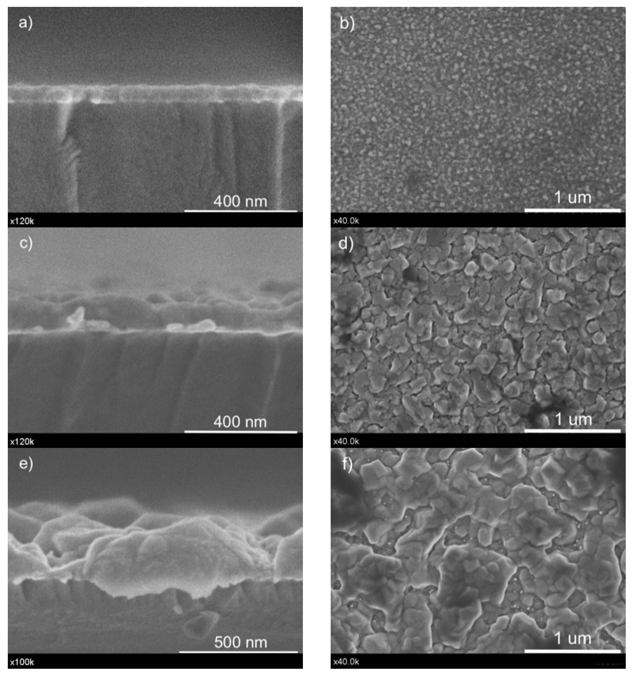
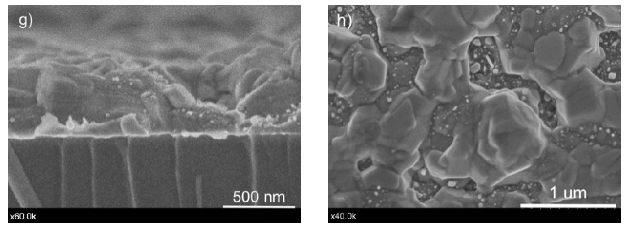
Cross-sectional and top view SEM images (
Figure 4) reveal an increasing surface roughness and the apparent transition from a two-dimensional (Frank–van der Merwe mode) to a three-dimensional thin film growth mode (Volmer–Weber mode) [
23]. While after 2 min deposition, the films have a closed microstructure, an open microstructure with big islands and deep voids approaching the substrate has evolved.
SEM analysis (
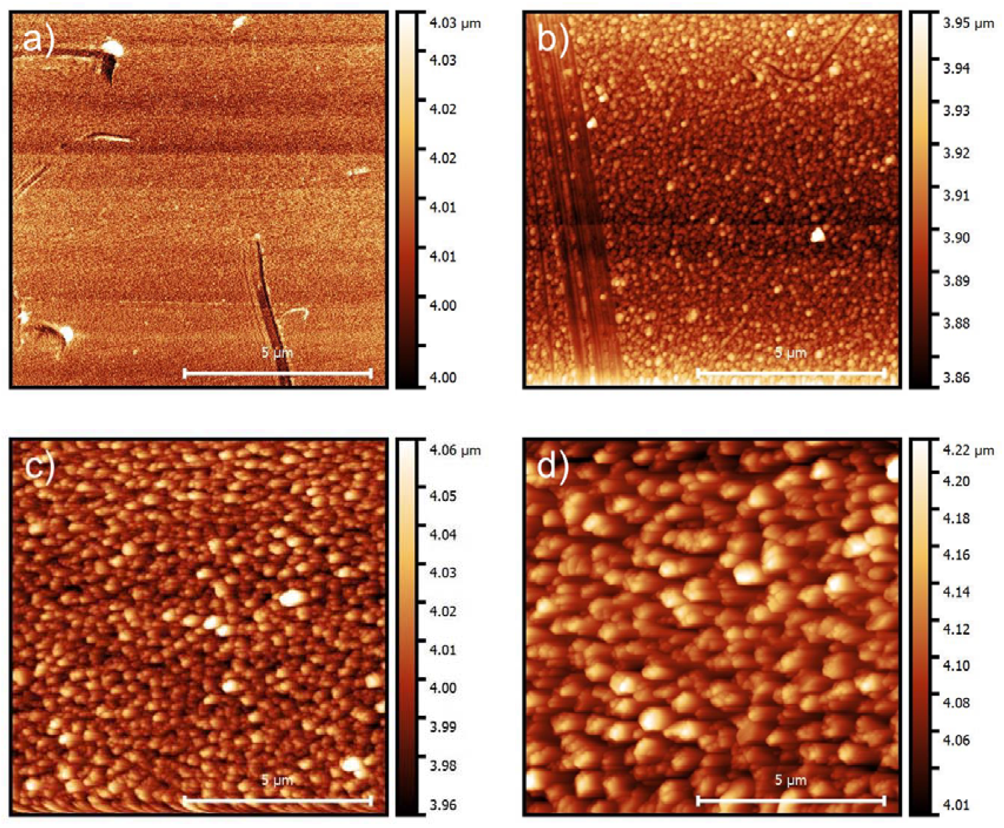
Figure 4) was complemented with AFM measurements. AFM images of 10 × 10 µm are shown in
Figure 5 for samples deposited at different times (
t = 2–20 min). The increase of surface roughness with deposition time is also evident in this scale. For short deposition times, the surface presents a very smooth and featureless morphology that turns into a granular morphology with a mean grain size growing from 170 nm at 5 min deposition time to 425 nm at 20 min deposition time.
In addition, the dynamics of the surface growth were characterized by means of a dynamic scaling theory (DST) approach [
24,
25]. In short, within the framework of DST, the roughness
σ is defined as the mean square deviation of the local height,
h, with respect to the mean height <
h(
t)>:
where
h(
r,
t) is the growing surface with
r a vector in the base plane,
t the deposition time, and <…> represents the average over all
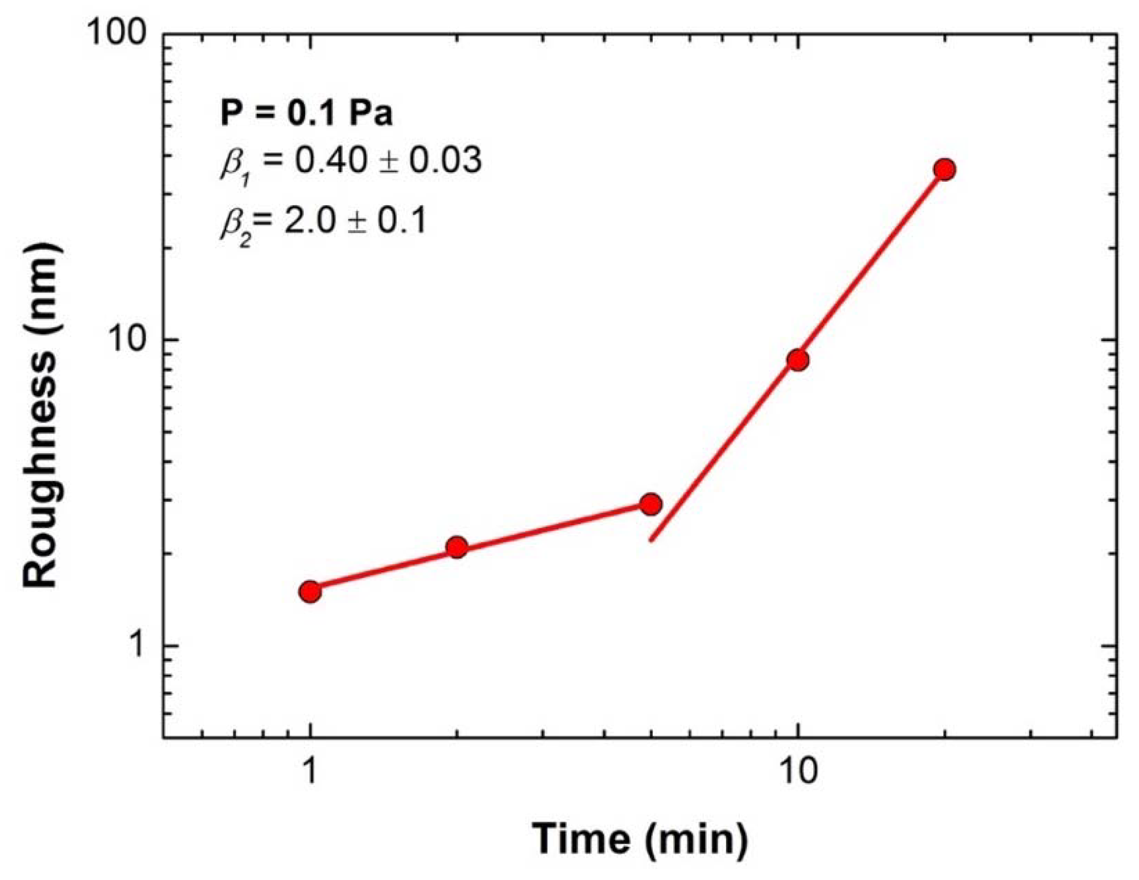
r in a given area. Under the assumptions of standard Family–Vicsek dynamic scaling, there are specific scaling relationships of the temporal and spatial dependences of σ. In particular, the evolution of the surface roughness with the deposition time: σ ≈
tβ. The growth exponent (β) can be determined by following the change of σ with time as can be observed in
Figure 6. From the log-log plot of the surface roughness at different deposition times, two different growth regimes can be observed. For deposition times below 5 min, there is a monotonous but slow increase of roughness with time σ ≈
t0.4. From this stage on, there is abrupt change in the growth dynamics and the surface roughness increases at a much faster pace σ ≈
t2.0.
The observed changes in the sample morphologies and, in particular, the two different growth mechanisms, are responsible for the optical properties of the deposited aluminium thin films. In
Figure 2, it is shown that samples prepared under short deposition times (2 and 5 min) showed a mirror-like appearance that turned into an opaque whitish colour for longer deposition times (10 and 20 min). As inferred from RBS results, this change in appearance cannot be attributed to a compositional change in the films (i.e., formation of a white alumina oxide layer due to the surface oxidation of aluminium). Contrarily, this change is related to a variation in the contribution of the specular component of the sample reflectance. In
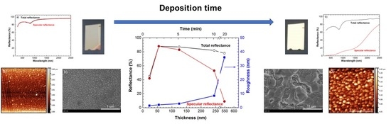
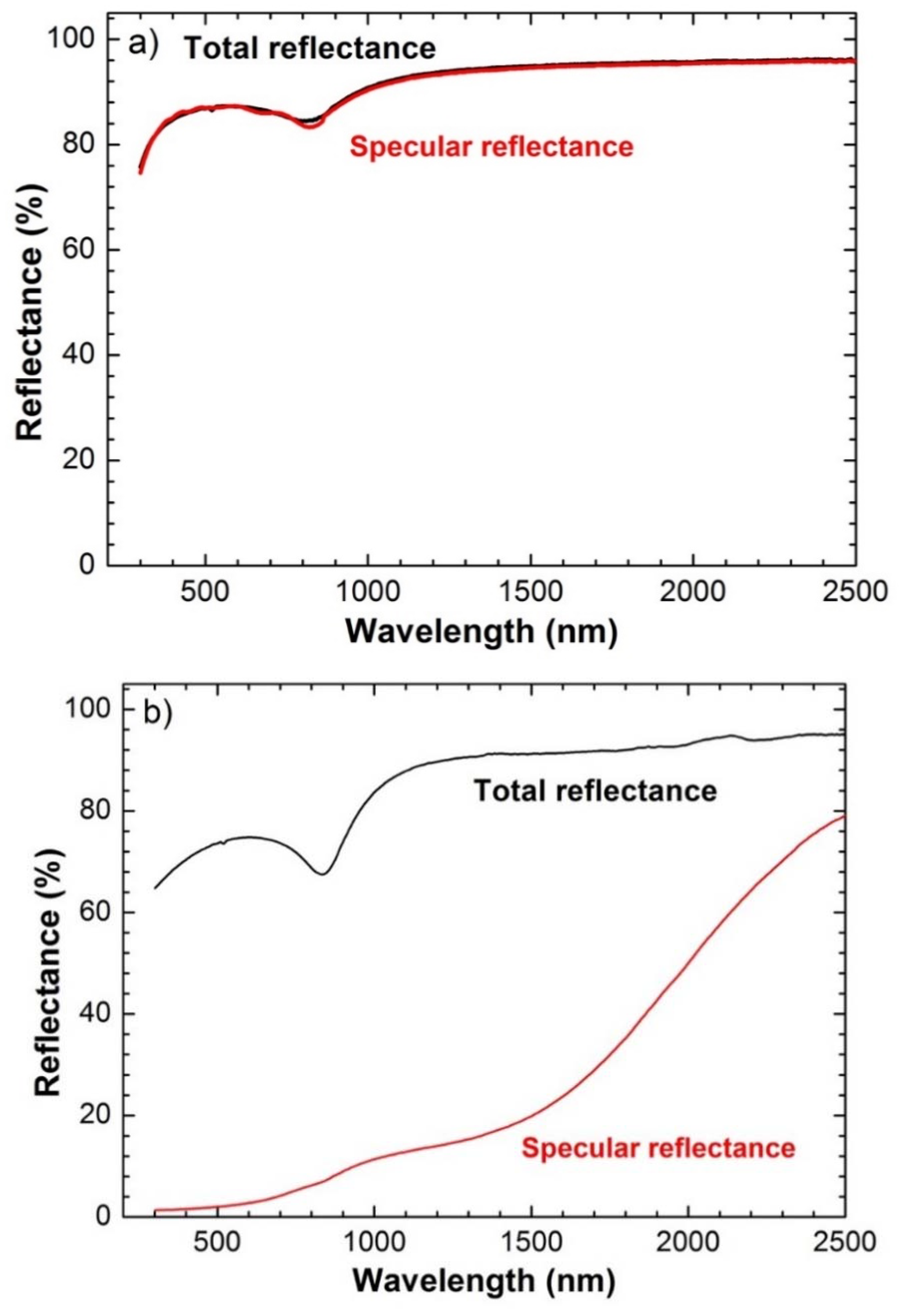
Figure 7, the total and specular reflectance are shown for the case of aluminium film deposited at 0.1 Pa for (top) 2 min and (bottom) 20 min. In the first case, the reflectance is almost purely specular (99.8% of the total reflectance), while the contribution of the specular reflectance to the total reflectance decreases enormously (down to 12%) for longer deposition times.
This behaviour correlates well with the observed changes in the surface roughness and grain size and the different growth regimes derived from DST analysis. In
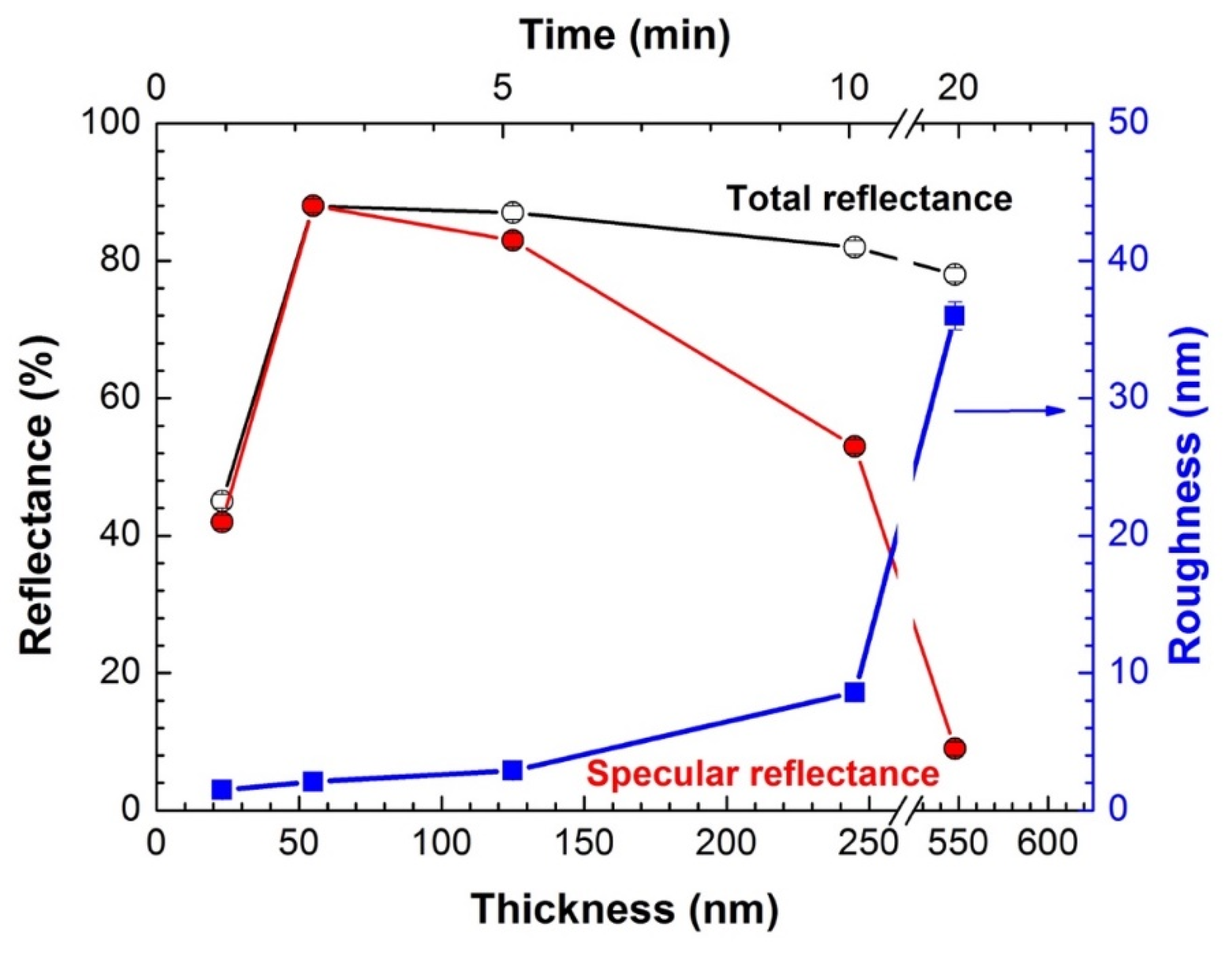
Table 3, the data of total and specular reflectance of the deposited samples are summarized and in
Figure 8, the total and specular reflectance together with the roughness of the samples are plotted versus the layer thickness. The thinnest layer of 22 nm (1 min deposition) still presents a semi-transparent performance with a total reflectance of around 42%. The total reflectance increases up to 87–88% with layer thickness for samples thinner than 120 nm (2 to 5 min deposition). This corresponds with the first regime of growth of DST that was characterised by a slow increase of the surface roughness (from 1.5 to 3 nm) and grain size with thickness. As stated above, the main contribution (99–95%) to this reflectance comes from the specular component and is in this range, at 2 min specifically, where best results for specular reflectance were measured. Although there is a small decrease of the total reflectance of thicker samples (78% for a 544 nm layer), probably related to light absorption, the most remarkable observation is the abrupt change of the specular reflectance of those samples. It decreases from 83% for a 122 nm layer down to 53% and 9% for 244 and 559 nm films, respectively. This behaviour is aligned with the increase up to an order of magnitude of the surface roughness of these samples (from 3 to 36 nm) and the appearance of large surface grains (>400 nm). It seems plausible that this increase of roughness and grain size produces the scattering of light on the thin film surface and, therefore, the diffuse component of the reflectance becomes predominant in these samples. It is worth noting that the thickest aluminium sample presents a relatively high total reflectance (around 80%) with a 90% diffuse component. This opens the possibility of using such films a diffuse metal standard as an alternative to typical commercial reference materials made, such as BaSO
4 or Spectralon used by commercial spectrophotometer manufacturers. It is important to remark that one of the great advantages of such a standard is that it could be complemented with a specular standard made of the same material (aluminium).
4. Conclusions
The aim of this paper was to optimise deposition parameters of aluminium thin films to obtain maximum specular reflectance using filtered cathodic vacuum arc. Deposition conditions of aluminium thin films were shown to have a massive impact on thin film properties and microstructure. The transparency of the samples increases with the working pressure (for a fixed deposition time) due to a decrease of the deposition rate of the samples. This is easily apparent already from the comparison of samples with similar thickness, but grown at different pressures and rates, namely the samples deposited in 2 min at 0.1 Pa and in 20 min at 1 Pa, respectively (
Figure 2). The resulting thicknesses of 56 nm and 40 nm are not much different. However, the first sample was well-reflecting, and the latter one was transparent. Working at a fixed pressure of 0.1 Pa, samples showed a transition from a mirror-like appearance to opaque whitish colour for longer deposition times. RBS spectra showed that this change in reflectance could not be attributed to the surface oxidation of the films, but to a dramatic increase (~20 times) of the surface roughness with deposition time. This increase was confirmed by SEM, profilometry, and AFM measurements. Consequently, the specular contribution to the total reflectance of the films dropped from 99.8% in the case of films deposited for 2 min, down to 12% in the case of films deposited for 20 min. These results were correlated with the presence of two different growth regimes as derived from dynamic scaling analysis. In the first regime (deposition times ≤5 min), the roughness slowly increases with time (σ ≈
t0.4) leading to the deposition of highly specular reflecting aluminium thin films. For longer deposition times, the surface roughness increases rapidly (σ ≈
t2.0) and highly diffusive reflecting aluminium films are grown.
The 88% maximum specular reflectance obtained with optimised aluminium thin films in this study is still far from the 95% values that solar collectors mirror uses today. However, it paves the way for further optimisation using the thin films developed here. This optimization would include exploring other experimental parameters (in particular, the growth temperature) and the deposition of dielectric multilayers on top of the metal film [
26].
These results could be also applied to create diffuse aluminium standard as an alternative to typical commercial materials as such BaSO4 or Spectralon. This can greatly contribute to the accuracy in the reflectance measurement and performance comparison of materials whose specular and diffuse components of the total reflectance are very much dependent on the deposition conditions.

 ,
, 


