Mechanical Properties of Zr–Si–N Films Fabricated through HiPIMS/RFMS Co-Sputtering

1
Department of Materials Engineering, Ming Chi University of Technology, New Taipei City 24301, Taiwan
2
Center for Plasma and Thin Film Technologies, Ming Chi University of Technology, New Taipei City 24301, Taiwan
3
Institute of Materials Engineering, National Taiwan Ocean University, Keelung 20224, Taiwan
*
Author to whom correspondence should be addressed.
Coatings 2018, 8(8), 263; https://doi.org/10.3390/coatings8080263
Submission received: 1 July 2018
/
Revised: 21 July 2018
/
Accepted: 26 July 2018
/
Published: 27 July 2018
(This article belongs to the Special Issue Design and Synthesis of Hard Coatings)
Abstract
:Zr–Si–N films were fabricated through the co-deposition of high-power impulse magnetron sputtering (HiPIMS) and radio-frequency magnetron sputtering (RFMS). The mechanical properties of the films fabricated using various nitrogen flow rates and radio-frequency powers were investigated. The HiPIMS/RFMS co-sputtered Zr–Si–N films were under-stoichiometric. These films with Si content of less than 9 at.%, and N content of less than 43 at.% displayed a face-centered cubic structure. The films’ hardness and Young’s modulus exhibited an evident relationship to their compressive residual stresses. The films with 2–6 at.% Si exhibited high hardness of 33–34 GPa and high Young’s moduli of 346–373 GPa, which was accompanied with compressive residual stresses from −4.4 to −5.0 GPa.
1. Introduction
Nanocomposite nitride films are comprised of nacocrystalline metal–nitride grains scattered in an amorphous Si3N4 matrix. These are recognized as nc-MenN/a-Si3N4 films, and have been widely investigated [1,2,3,4]. A hardness of 50 GPa was attained for nc-TiN/a-Si3N4 films, which was attributed to the inhibition of crack propagation by the amorphous tissue surrounding the nanocrystals [1]. The Ti–Si–N films with 8 at.% Si exhibited maximum hardness [1,2]. Previous studies [5,6,7] have applied the nc-MenN/a-Si3N4 model to interpret the hardness improvement of Nb–Si–N films, which exhibited a hardness of 34 GPa accompanied with the addition of 5–13 at.% Si. However, the hardness enhancement for Nb–Si–N films is restricted in contrast to that for Ti–Si–N films. Moreover, the previous works on Zr–Si–N films [8,9,10,11] also exhibited restricted improvement in hardness as the addition of 2–6 at.% Si achieved a hardness of 30–36 GPa. Additionally, the reported strengthening mechanisms were not consistent. The nc-MenN/a-Si3N4 model could not be applied to most Si-containing metal-nitride films. In our previous studies on Ta–Si–N [12], Nb–Si–N [13] and Zr–Si–N [14] coatings, fabricated using direct-current magnetron sputtering (DCMS) (introducing high Si contents into nitrides), formed an amorphous structure on X-ray and improved the oxidation resistance; although their mechanical properties deteriorated. Therefore, high-Si-content Ta–Si–N [15] and Zr–Si–N [16] coatings are applied for glass molding dies, which are operated under a low oxygen-containing atmosphere at approximately 600 °C. By contrast, the low-Si-content Zr–Si–N coatings exhibited a crystalline structure accompanied with a hardness level of 23–24 GPa and a compressive stress of less than 2 GPa [14]. High-power impulse magnetron sputtering (HiPIMS) [17,18] was recommended to grow films with a dense structure, high hardness and high residual compressive stress [19,20]. Therefore, exploring the mechanical performance of low-Si-content Zr–Si–N films fabricated by HiPIMS is essential for extending potential practical applications. Because the HiPIMS process resulted in low deposition rates [18], hybrid HiPIMS/DCMS [21] and HiPIMS/RFMS (radio-frequency magnetron sputtering) [22] were utilized to raise the deposition rate. In a previous study [23], the ZrNx films prepared using HiPIMS system exhibited a nanoindentation hardness level of 26–27 GPa. In this study, Zr–Si–N films were fabricated through HiPIMS/RFMS hybrid process, before the mechanical properties of these films were investigated.
2. Materials and Methods
Figure 1 shows the schematic of HiPIMS/RFMS co-sputtering system. A target of 99.999% pure Si was connected to a RF (radio-frequency) power generator (13.56 MHz), while the targets of 99.995% Ti and 99.9% Zr were connected to a pulse power supply (SPIK 2000A; Shen Chang Electric Co., Ltd., Taipei, Taiwan) operated in the unipolar negative mode. The Si, Ti, and Zr targets were 50.8, 76.2 and 76.2 mm in diameter, respectively. The chamber was pumped to a base pressure of 6.7 × 10⁻⁴ Pa using a turbopump (TURBOVAC 600C, Leybold, Hsinchu, Taiwan) and monitored by an ionization gauge (274005, Granville-Phillips Company, Longmont, CO, USA). The substrate-to-target distance was 12 cm. The substrate holder without heating was rotated at 10 rpm and was grounded. The substrate holder was maintained at less than 70 °C during the deposition, which resulted in an insignificant thermal stress of less than 0.1 GPa. A working pressure of 0.4 Pa was formed after introducing 30-sccm-Ar flow into the chamber, before Ti was deposited at 400 W for 40 min. This creates an interlayer on silicon substrates, which had a thickness of 80–100 nm. Subsequently, Zr–Si–N films were co-sputtered on Ti interlayers after flowing a gas mixture of Ar and N2 into the chamber. The sum of the Ar and N2 flow rates were maintained at 30 sccm and the working pressure was maintained at 0.4 Pa. The HiPIMS process was conducted using the pulse on-time (ton) and pulse off-time (toff) of 100 and 3900 µs, respectively, which resulted in a duty cycle of 2.5% and a repetition frequency of 250 Hz. Table 1 lists the main variables for depositing Zr–Si–N films. Batch I samples were prepared using various nitrogen flow rates, while Batch II samples were prepared using various sputter powers. The chemical compositions of the films were analyzed using a field-emission electron probe microanalyzer (FE-EPMA, JXA-8500F, JEOL, Akishima, Japan). The PET (pentaerythritol), TAP (Thallium acid phthalate), and LDE1 (layered diffracting elements of W and Si) crystals were used to analyze Zr, Si, as well as N, and O, respectively. The samples were labeled as ZrxSiyN100−x−y. The film thicknesses determined on the fracture surface were evaluated by field emission scanning electron microscopy (FE-SEM, S4800, Hitachi, Tokyo, Japan). Grazing-incident X-ray diffraction (GIXRD) was performed by using an X-ray diffractometer (XRD, X’Pert PRO MPD, PANalytical, Almelo, The Netherlands) to identify the phases. The incidence angle was 1°. Moreover, the XRD patterns were obtained by the Bragg–Brentano (θ–2θ) scan to calculate lattice parameters and texture coefficients. The nanostructure of the films was observed using transmission electron microscopy (TEM, JEM-2010F, JEOL, Akishima, Japan). The TEM samples with a protective Pt layer were produced using a focused ion beam system (FEI Nova 200, Hillsboro, OR, USA). The mechanical properties, hardness and Young’s modulus of the films were evaluated using a nanoindentation tester (TI-900 Triboindenter, Hysitron, Minneapolis, MN, USA) and calculated using the Oliver and Pharr method [24]. An atomic force microscope (AFM, DI 3100, Bruker, Santa Barbara, CA, USA) recorded the surface roughness. The residual stress of the films was measured by the curvature method [25].
3. Results and Discussion
3.1. Zr–Si–N Films Fabricated Using Various Nitrogen Flow Rates
Table 2 shows the chemical compositions of the Batch I films fabricated using various nitrogen flow rates. The O contents of the Zr–Si–N films were in the range of 0.3–1.2 at.%. The N content of the films increased from 40 to 43, 45, 46, and 47 at.% when the nitrogen flow rate was increased from 2.0 to 2.5, 3.0, 3.5, and 4.0 sccm, respectively. The Si content was changed from 8 to 9, 10, 10, and 10 at.%, respectively. The film thickness was maintained at levels of 720–898 nm by adjusting the deposition times. Figure 2 exhibits an evident decrease in the deposition rate from 4.0 to 2.5 nm/min as the nitrogen flow rate is increased from 2.0 to 4.0 sccm. The decrease was attributed to the highly ionized reactive gas used in the HiPIMS process, which had a severe poisoning effect of the Zr target [26,27,28].
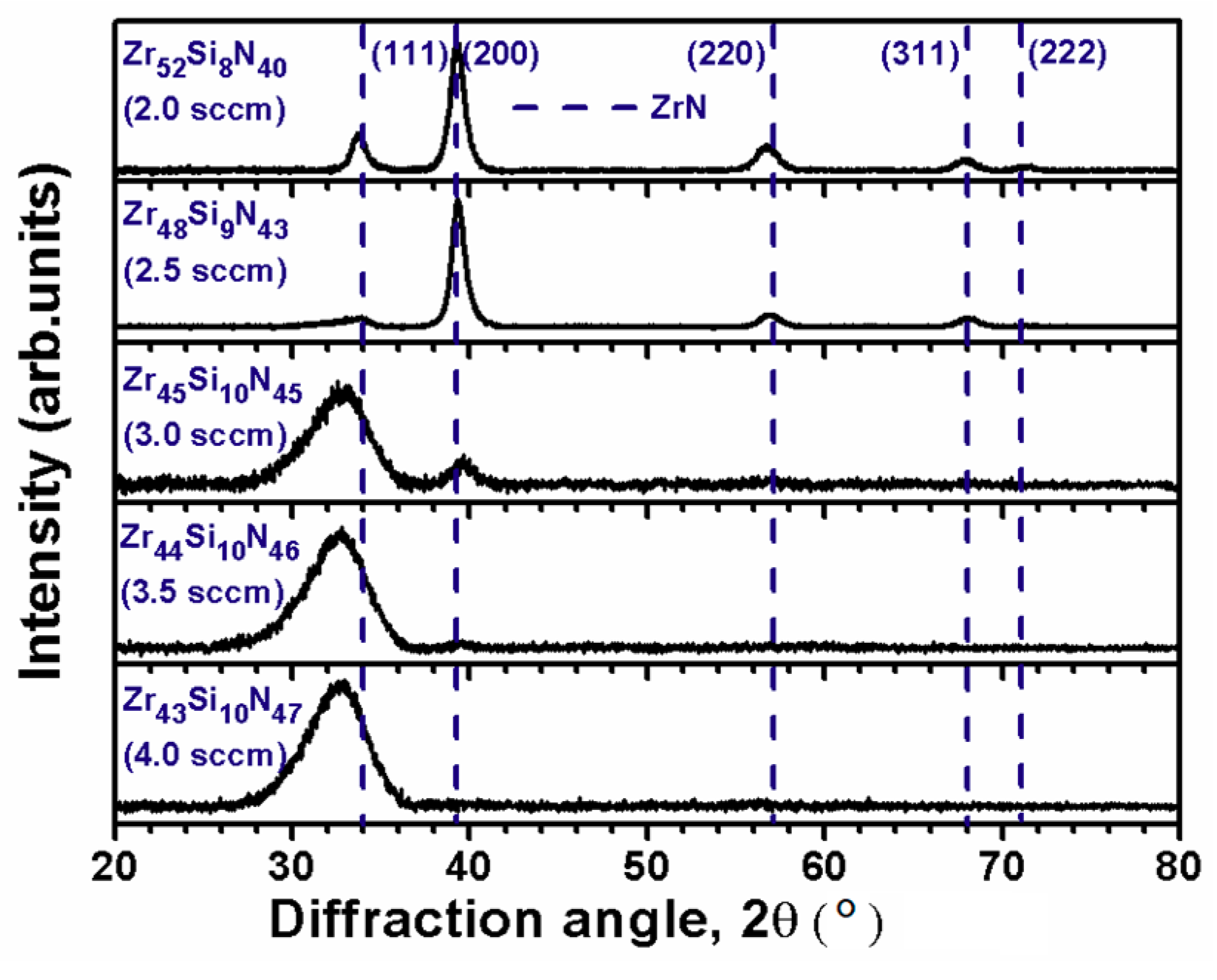
Figure 3 depicts the GIXRD patterns of the Zr–Si–N films. The Zr52Si8N40 and Zr48Si9N43 films displayed a face-centered cubic (fcc) ZrN (ICDD 35-0753) phase; the Zr45Si10N45 films exhibited mixed fcc ZrN and X-ray amorphous phases; and the Zr44Si10N46 and Zr43Si10N47 films were found to have an X-ray amorphous phase. Although the differences in Si and N contents between these films were not large, the structure varied evidently. The films with Si content of less than 9 at.% and N content less than 43 at.% exhibited a fcc structure, while the films with Si and N contents above the limitations exhibited an amorphous phase-dominated structure.
Table 2 lists the surface roughness, hardness, Young’s modulus and residual stress values of Zr–Si–N films. The crystalline Zr52Si8N40 and Zr48Si9N43 films exhibited relatively high surface roughness levels (Ra) of 3.5 and 2.2 nm, respectively. The Zr45Si10N45 films revealed the lowest roughness level of 0.3 nm, while the amorphous Zr44Si10N46 and Zr43Si10N47 films exhibited a roughness level of 1.1 nm. Figure 4 shows the variations of hardness and residual stress related to different N2 flow rates. The hardness values of crystalline Zr52Si8N40 and Zr48Si9N43 films were 27.4 and 20.4 GPa, respectively, which were accompanied with residual stress of −2.8 and −1.6 GPa, respectively. In contrast, the Zr45Si10N45, Zr44Si10N46 and Zr43Si10N47 films exhibited a hardness level of 13.8–14.5 GPa, which was accompanied with the presence of an amorphous. This resulted in a low residual stress level of −0.2 to −0.6 GPa. The elastic moduli and hardness of Zr–Si–N films displayed similar variations related to their chemical compositions. Additionally, the H3/E2 values, which represent resistance to plastic deformation [29], were 0.31 and 0.14 GPa for the crystalline Zr52Si8N40 and Zr48Si9N43 films, respectively. By contrast, the Zr45Si10N45, Zr44Si10N46 and Zr43Si10N47 films containing an amorphous phase exhibited a low H3/E2 level of 0.08–0.09 GPa.
3.2. Zr–Si–N Films Fabricated Using Various Power Levels
The Batch II films were fabricated through HiPIMS/RFMS co-sputtering using an average HiPIMS power of 300 W on the Zr target and various RF powers on the Si target (Table 1). The O contents of the films were 0.2–0.9 at.% (Table 2). The N content of the Batch II samples was changed from 29 to 36, 35, 37, 38, 40, and 40 at.% as the RF power increased from 0 to 25, 30, 35, 40, 50 and 60 W, respectively, and the Si content varied from 0, to 2, 3, 5, 6, 8, and 10 at.%, respectively. Both Batches I and II samples exhibited an atomic ratio N/(Zr + Si) of 0.41–0.89, which is under the stoichiometric ratio of 1.0 for ZrN. In a previous study [22], Ta–Zr–N films fabricated by the same HiPIMS/RFMS co-sputtering also exhibited an under-stoichiometric N/(Ta + Zr) ratio of 0.40–0.68. In another previous work [23], ZrNx films prepared using HiPIMS system exhibited an under-stoichiometric N/Zr ratio of 0.65–0.78. The deposition times for Batch II processes were adjusted to fabricate films with similar thickness values of 831–1183 nm. The deposition rates increased from 3.0 to 4.2 nm/min when increasing the RF power from 0 to 60 W.
Figure 5 displays the GIXRD patterns of the Zr–Si–N films with various Si content. The Zr71N29 films exhibited a fcc ZrN structure with a strong (111) reflection. The introduction of Si into the films caused the structure to exhibit a strong (200) reflection, while the (111) reflection diminished. The fcc reflections became broadened and shifted toward the right side with further increases in the Si content in the films. Figure 6 and Figure 7 show the XRD patterns under a Bragg–Brentano scan and their texture coefficients [30,31] of the Batch II films, respectively. The reflections of Ti [ICDD 44-1294], TiSi [ICDD 17-0424] and ZrSi2 [ICDD 32-1499] phases were observed besides a ZrN phase. The Ti and TiSi reflections were presented in another Ti/Si sample (not shown in this paper). The preferred orientations were (111) and (200) for the films with Si contents of <6 at.% and >8 at.%, respectively. Figure 8 exhibits the lattice parameters and grain sizes of the Zr–Si–N films calculated using (111) reflections. The lattice parameters decreased when increasing the Si content from 0 to 8 at.% due to the small atomic size of Si compared to Zr. This implied that 8 at.% Si or part of the 8 at.% Si was solved in the ZrN matrix and the residual Si atoms may reside at grain boundaries. Sandu et al. [7] suggested a solubility limit of 4 at.% Si for Nb–Si–N and Zr–Si–N films. A three-region model interpreted the structural evolution of composite M–Si–N films, which included the solubility of Si, coverage layer of SiNx at grain boundaries and reduction of crystallite size. In contrast, the lattice parameters of the Zr50Si10N40 films with a higher Si content of 10 at.% were larger than those of the films with 4–6 at.% Si, which could be attributed to the coexistence of Zr3N4 [16]. The grain sizes of the Batch II films determined by the Scherrer formula [32] exhibited a decreasing trend from 19.8 to 17.3, 17.7, 10.6 and 8.1 nm when increasing the Si contents from 0 to 3, 6, 8 and 10 at.%.
Figure 9a, Figure 10a and Figure 11a show the cross-sectional TEM images of the Zr71N29, Zr62Si3N35 and Zr50Si10N40 films, respectively. The selected area electron diffraction (SAED) patterns of the Zr71N29 and Zr62Si3N35 films in Figure 9a and Figure 10a indicated a fcc ZrN phase, while the SAED pattern of the Zr50Si10N40 films consisted of continuous rings, which implies a nanostructure. The high-magnification images of the Zr71N29 and Zr62Si3N35 films (Figure 9b and Figure 10b) exhibited a columnar structure with widths of 19–22 and 14–17 nm, respectively. Figure 11b shows that the Zr50Si10N40 films exhibits a fine structure and the width of the short columnar structure narrows to 9 nm only. The widths of the columnar structure in the Zr–Si–N films displayed a decreasing trend with increasing the Si content, which were consistent with the calculated grain sizes from XRD evaluation (Figure 8). Moreover, the short columnar structure of the Zr50Si10N40 films that represented the crystalline regions were interrupted by amorphous tissue in the growth direction. Therefore, the lattice parameters of the Zr50Si10N40 films did not follow the variation tendency of the Zr–Si–N films with 0–8 at.% Si, and the solid solution strengthening by introducing Si into ZrN matrix were negligible for the Zr50Si10N40 films.
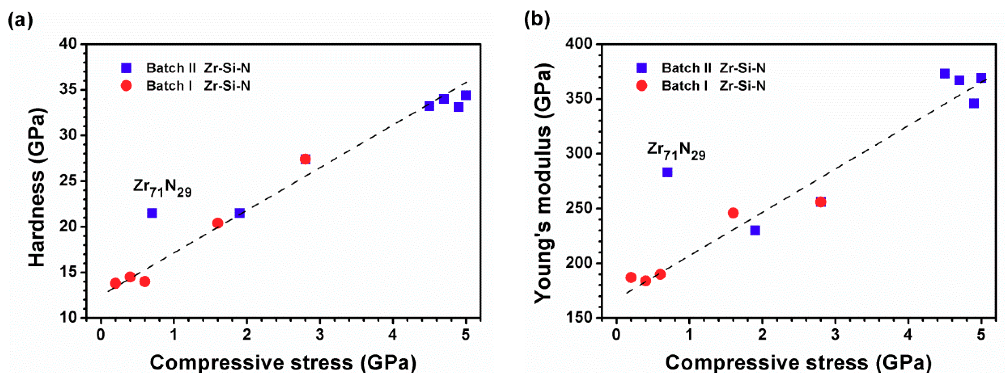
Table 2 and Figure 12 shows the hardness and residual stresses of the Zr–Si–N films with various Si contents. The Zr71N29 films exhibited a hardness of 21.5 GPa and a low compressive residual stress of −0.6 GPa, while the hardness were 33.1–34.3 GPa for the films with 2–6 at.% Si. This was accompanied with an elevated compressive residual stress level from −4.4 to −5.0 GPa. A further increase in Si content to 8 and 10 at.% resulted in decreased hardness of 27.4 and 21.5 GPa, respectively, which was accompanied with a decrease in the residual stress values to −2.8 and −1.8 GPa, respectively. The low-Si-content films exhibited a solid solution strengthening effect, while the formation of amorphous Si3N4 for high-Si-content films decreased the mechanical properties and relaxed the residual stress. Most of the previous studies on Zr–Si–N films reported a maximum hardness, which was accompanied with a certain range of Si contents [7,8,9,10]. Dong et al. [10], Martin et al. [9] and Mae et al. [8] reported maximum hardness of 29.8 GPa at 6.2 at.% Si, 36 GPa at 2 at.% Si and 35 GPa at 3 at.% Si, respectively. In the study conducted by Martin et al. [9], the films with a hardness of 36 GPa exhibited a stress of −5.7 GPa and a grain size of 17 nm. These characteristics seemed similar to the reported data in this study. The variation of hardness was evidently related to that of the residual stress [8,14]. Figure 13a shows the relationship of hardness and residual stress for Batches I and II samples, which exhibits a linear trend except for the hardness of Zr71N29 films. A similar linear relationship between Young’s modulus and residual stress was shown in Figure 13b. Table 2 shows that the Zr–Si–N films with 2–6 at.% Si shows high H3/E2 levels of 0.26–0.30 GPa, which was accompanied with low roughness levels of 0.8–1.4 nm.
4. Conclusions
Under-stoichiometric Zr–Si–N films with atomic ratios N/(Zr + Si) of 0.41–0.89 were fabricated through HiPIMS/RFMS co-sputtering. The structural characteristics of Zr–Si–N films was influenced by their constitutions. The films with Si content of less than 9 at.% and N content of less than 43 at.% displayed a face-centered cubic structure. The mechanical properties of Zr–Si–N films exhibited linear tendencies that were related to their residual stresses. The crystalline Zr–Si–N films of 2–6 at.% Si showed a high nanoindentation hardness level of 33.1–34.3 GPa and a high Young’s modulus level of 346–373 GPa, which demonstrated H3/E2 values of 0.26–0.30 GPa and surface roughness of 0.8–1.4 nm.
Author Contributions
Conceptualization, L.-C.C.; Data Curation, L.-C.C.; Formal Analysis, Y.-I.C.; Funding Acquisition, L.-C.C. and Y.-I.C.; Investigation, Y.-Z.Z.; Project Administration, L.-C.C.; Resources, L.-C.C.; Writing-Original Draft Preparation, L.-C.C. and Y.-I. C.
Funding
This research was funded by the Ministry of Science and Technology, Taiwan (106-2221-E-131-002 and 105-2221-E-019-007-MY3). The APC was funded by Ming Chi University of Technology.
Acknowledgments
The authors thank Mei-Chen Chiang at Ming Chi University of Technology for the technical support of TEM observations.
Conflicts of Interest
The authors declare no conflict of interest.
References
- Vepřek, S.; Haussmann, M.; Reiprich, S.; Li, S.; Dian, J. Novel thermodynamically stable and oxidation resistant superhard coating materials. Surf. Coat. Technol. 1996, 86–87, 394–401. [Google Scholar] [CrossRef]
- Veprek, S.; Niederhofer, A.; Moto, K.; Bolom, T.; Männling, H.-D.; Nesladek, P.; Dollinger, G.; Bergmaier, A. Composition, nanostructure and origin of the ultrahardness in nc-TiN/a-Si3N4/a- and nc-TiSi2 nanocomposites with HV = 80 to ≥105 GPa. Surf. Coat. Technol. 2000, 133–134, 152–159. [Google Scholar] [CrossRef]
- Diserens, M.; Patscheider, J.; Lévy, F. Mechanical properties and oxidation resistance of nanocomposite TiN–SiNx physical-vapor-deposited thin films. Surf. Coat. Technol. 1999, 120–121, 158–165. [Google Scholar] [CrossRef]
- Vaz, F.; Rebouta, L.; Goudeau, P.; Pacaud, J.; Garem, H.; Rivière, J.P.; Cavaleiro, A.; Alves, E. Characterisation of Ti1−xSixNy nanocomposite films. Surf. Coat. Technol. 2000, 133–134, 307–313. [Google Scholar] [CrossRef]
- Benkahoul, M.; Sandu, C.S.; Tabet, N.; Parlinska-Wojtan, M.; Karimi, A.; Lévy, F. Effect of Si incorporation on the properties of niobium nitride films deposited by DC reactive magnetron sputtering. Surf. Coat. Technol. 2004, 188–189, 435–439. [Google Scholar] [CrossRef]
- Sandu, C.S.; Benkahoul, M.; Sanjinés, R.; Lévy, F. Model for the evolution of Nb–Si–N thin films as a function of Si content relating the nanostructure to electrical and mechanical properties. Surf. Coat. Technol. 2006, 201, 2897–2903. [Google Scholar] [CrossRef]
- Sandu, C.S.; Sanjinés, R.; Benkahoul, M.; Medjani, F.; Lévy, F. Formation of composite ternary nitride thin films by magnetron sputtering co-deposition. Surf. Coat. Technol. 2006, 201, 4083–4089. [Google Scholar] [CrossRef]
- Mae, T.; Nose, M.; Zhou, M.; Nagae, T.; Shimamura, K. The effects of Si addition on the structure and mechanical properties of ZrN thin films deposited by an r.f. reactive sputtering method. Surf. Coat. Technol. 2001, 142–144, 954–958. [Google Scholar] [CrossRef]
- Martin, P.J.; Bendavid, A.; Cairney, J.M.; Hoffman, M. Nanocomposite Ti–Si–N, Zr–Si–N, Ti–Al–Si–N, Ti–Al–V–Si–N thin film coatings deposited by vacuum arc deposition. Surf. Coat. Technol. 2005, 200, 2228–2235. [Google Scholar] [CrossRef]
- Dong, Y.; Zhao, W.; Li, Y.; Li, G. Influence of silicon on the microstructure and mechanical properties of Zr–Si–N composite films. Appl. Surf. Sci. 2006, 252, 5057–5062. [Google Scholar] [CrossRef]
- Choi, H.; Jang, J.; Zhang, T.; Kim, J.H.; Park, I.W.; Kim, K.H. Effect of Si addition on the microstructure, mechanical properties and tribological properties of Zr–Si–N nanocomposite coatings deposited by a hybrid coating system. Surf. Coat. Technol. 2014, 259, 707–713. [Google Scholar] [CrossRef]
- Chen, Y.I.; Lin, K.Y.; Wang, H.H.; Cheng, Y.R. Characterization of Ta–Si–N coatings prepared using direct current magnetron co-sputtering. Appl. Surf. Sci. 2014, 305, 805–816. [Google Scholar] [CrossRef]
- Chen, Y.I.; Gao, Y.X.; Chang, L.C.; Ke, Y.E.; Liu, B.W. Mechanical properties, bonding characteristics, and oxidation behaviors of Nb–Si–N coatings. Surf. Coat. Technol. 2018, in press. [Google Scholar] [CrossRef]
- Chen, Y.I.; Chang, S.C.; Chang, L.C. Oxidation resistance and mechanical properties of Zr–Si–N coatings with cyclic gradient concentration. Surf. Coat. Technol. 2017, 320, 168–173. [Google Scholar] [CrossRef]
- Chen, Y.I.; Cheng, Y.R.; Chang, L.C.; Lu, T.S. Chemical inertness of Ta–Si–N coatings in glass molding. Thin Solid Films 2015, 584, 66–71. [Google Scholar] [CrossRef]
- Chang, L.C.; Zheng, Y.Z.; Chen, Y.I.; Chang, S.C.; Liu, B.L. Bonding characteristics and chemical inertness of Zr–Si–N coatings with a high Si content in glass molding. Coatings 2018, 8, 181. [Google Scholar] [CrossRef]
- Kouznetsov, V.; Macák, K.; Schneider, J.M.; Helmersson, U.; Petrov, I. A novel pulsed magnetron sputter technique utilizing very high target power densities. Surf. Coat. Technol. 1990, 122, 290–293. [Google Scholar] [CrossRef]
- Helmersson, U.; Lattemann, M.; Bohlmark, J.; Ehiasarian, A.P.; Gudmundsson, J.T. Ionized physical vapor deposition (IPVD): A review of technology and applications. Thin Solid Films 2006, 513, 1–24. [Google Scholar] [CrossRef] [Green Version]
- Purandare, Y.P.; Ehiasarian, A.P.; Hovsepian, P.E. Structure and properties of ZrN coatings deposited by high power impulse magnetron sputtering technology. J. Vac. Sci. Technol. A 2011, 29, 011004. [Google Scholar] [CrossRef] [Green Version]
- Ehiasarian, A.P.; Münz, W.-D.; Hultman, L.; Helmersson, U.; Petrov, I. High power pulsed magnetron sputtered CrNx films. Surf. Coat. Technol. 2003, 163, 267–272. [Google Scholar] [CrossRef]
- Greczynski, G.; Lu, J.; Jensen, J.; Bolz, S.; Kölker, W.; Schiffers, C.; Lemmer, O.; Greene, J.E.; Hultman, L. A review of metal-ion-flux-controlled growth of metastable TiAlN by HIPIMS/DCMS co-sputtering. Surf. Coat. Technol. 2014, 257, 15–25. [Google Scholar] [CrossRef] [Green Version]
- Chang, L.C.; Chang, C.Y.; You, Y.W. Ta–Zr–N thin films fabricated through HIPIMS/RFMS co-sputtering. Coatings 2017, 7, 189. [Google Scholar] [CrossRef]
- Chang, L.C.; Chang, C.Y.; Chen, Y.I.; Kao, H.L. Mechanical properties and oxidation behavior of ZrNx thin films fabricated through high-power impulse magnetron sputtering deposition. J. Vac. Sci. Technol. A 2016, 34, 02D107. [Google Scholar] [CrossRef]
- Oliver, W.C.; Pharr, G.M. An improved technique for determining hardness and elastic modulus using load and displacement sensing indentation experiments. J. Mater. Res. 1992, 7, 1564–1583. [Google Scholar] [CrossRef]
- Janssen, G.C.A.M.; Abdalla, M.M.; van Keulen, F.; Pujada, B.R.; van Venrooy, B. Celebrating the 100th anniversary of the Stoney equation for film stress: Developments from polycrystalline steel strips to single crystal silicon wafers. Thin Solid Films 2009, 517, 1858–1867. [Google Scholar] [CrossRef]
- Audronis, M.; Bellido-Gonzalez, V.; Daniel, B. Control of reactive high power impulse magnetron sputtering processes. Surf. Coat. Technol. 2010, 204, 2159–2164. [Google Scholar] [CrossRef]
- Purandare, Y.P.; Ehiasarian, A.P.; Hovsepian, P.E. Target poisoning during CrN deposition by mixed high power impulse magnetron sputtering and unbalanced magnetron sputtering technique. J. Vac. Sci. Technol. A 2016, 34, 041502. [Google Scholar] [CrossRef] [Green Version]
- Anders, A. Tutorial: Reactive high power impulse magnetron sputtering (R-HiPIMS). J. Appl. Phys. 2017, 121, 171101. [Google Scholar] [CrossRef] [Green Version]
- Tsui, T.Y.; Pharr, G.M.; Oliver, W.C.; Bhatia, C.S.; White, R.L.; Anders, S.; Anders, A.; Brown, I.G. Nanoindentation and nanoscratching of hard carbon coatings for magnetic disks. Mater. Res. Soc. Symp. Proc. 1995, 383, 447–452. [Google Scholar] [CrossRef]
- Cheng, H.E.; Hon, M.H. Texture formation in titanium nitride films prepared by chemical vapor deposition. J. Appl. Phys. 1996, 79, 8047–8053. [Google Scholar] [CrossRef]
- Jones, M.I.; McColl, I.R.; Grant, D.M. Effect of substrate preparation and deposition conditions on the preferred orientation of TiN coatings deposited by RF reactive sputtering. Surf. Coat. Technol. 2000, 132, 143–151. [Google Scholar] [CrossRef]
- Cullity, B.D.; Stock, S.R. Elements of X-Ray Diffraction, 3rd ed.; Prentice Hall: Upper Saddle River, NJ, USA, 2001. [Google Scholar]
Figure 1.
Schematic of the high-power impulse magnetron sputtering (HiPIMS) and radio-frequency magnetron sputtering (RFMS) co-sputtering equipment.
Figure 1.
Schematic of the high-power impulse magnetron sputtering (HiPIMS) and radio-frequency magnetron sputtering (RFMS) co-sputtering equipment.
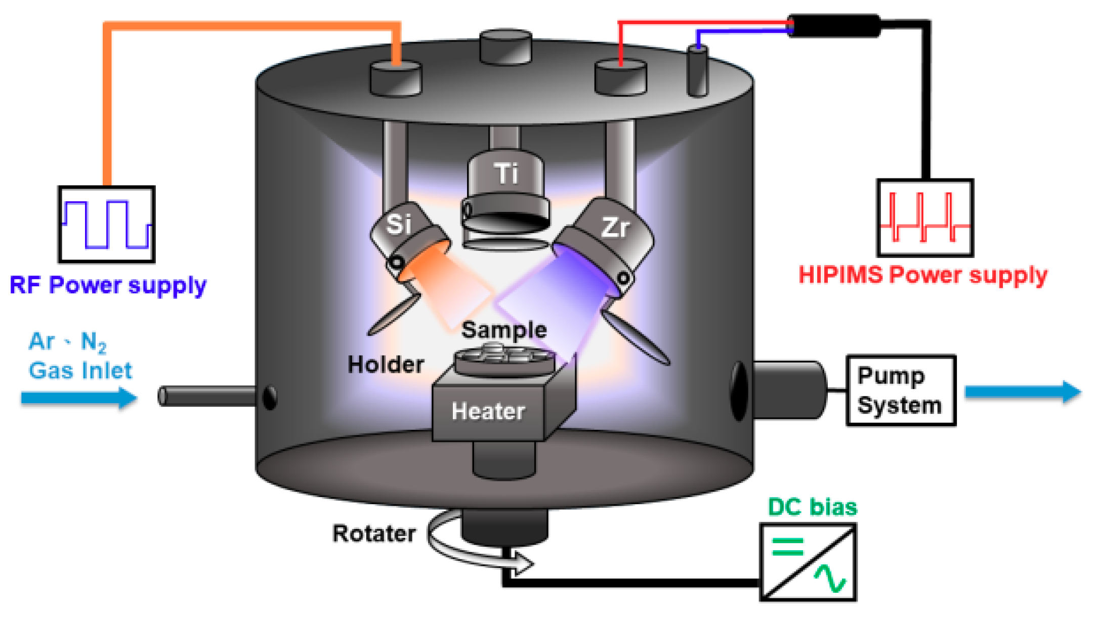
Figure 2.
Deposition rates of Batch I Zr–Si–N films fabricated using various nitrogen flow rates.
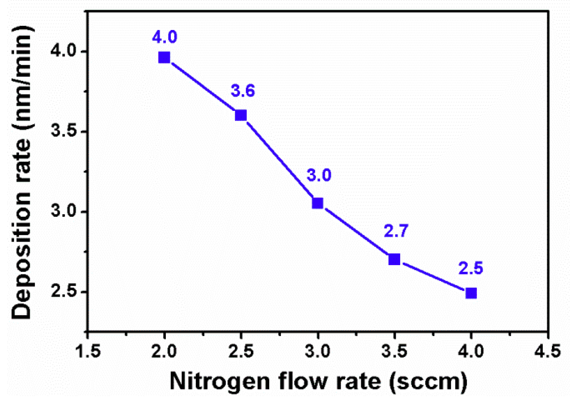
Figure 3.
Grazing-incident X-ray diffraction (GIXRD) patterns of Zr–Si–N films fabricated using various nitrogen flow rates.
Figure 3.
Grazing-incident X-ray diffraction (GIXRD) patterns of Zr–Si–N films fabricated using various nitrogen flow rates.

Figure 4.
Nanoindentation hardness and residual stress values of Zr–Si–N films fabricated using various nitrogen flow rates.
Figure 4.
Nanoindentation hardness and residual stress values of Zr–Si–N films fabricated using various nitrogen flow rates.
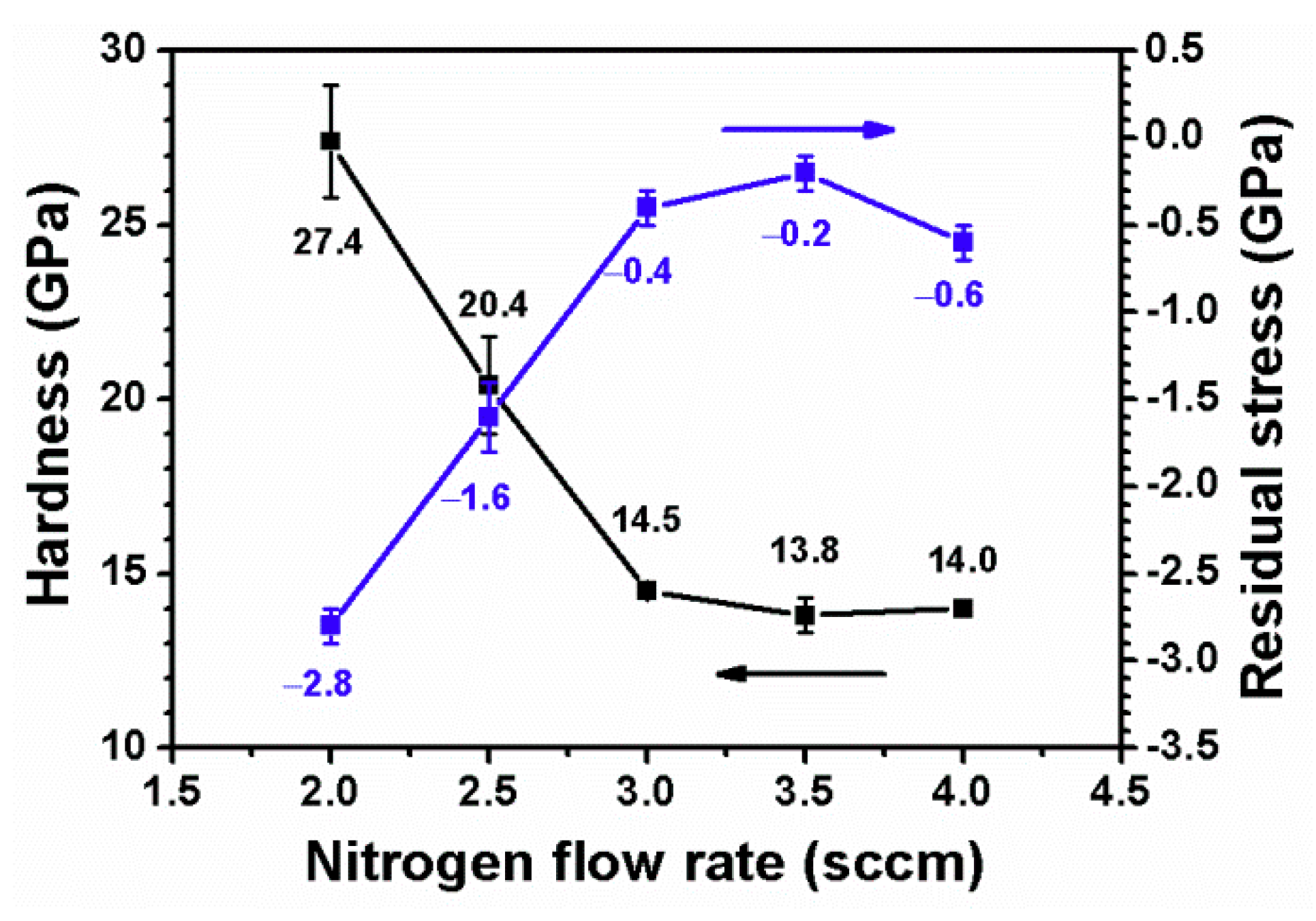
Figure 5.
Grazing-incident X-ray diffraction (GIXRD) patterns of Zr–Si–N films prepared using various RF powers on Si target.
Figure 5.
Grazing-incident X-ray diffraction (GIXRD) patterns of Zr–Si–N films prepared using various RF powers on Si target.
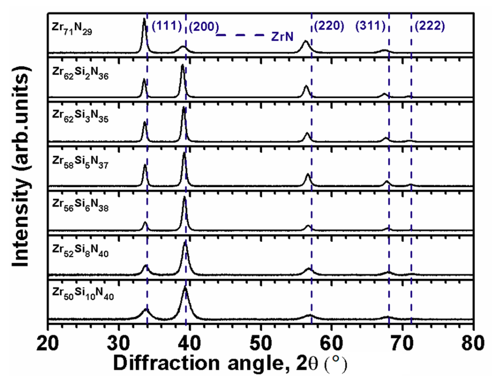
Figure 6.
Bragg–Brentano scan X-ray diffraction (XRD) patterns of Zr–Si–N films with a Ti interlayer.
Figure 6.
Bragg–Brentano scan X-ray diffraction (XRD) patterns of Zr–Si–N films with a Ti interlayer.
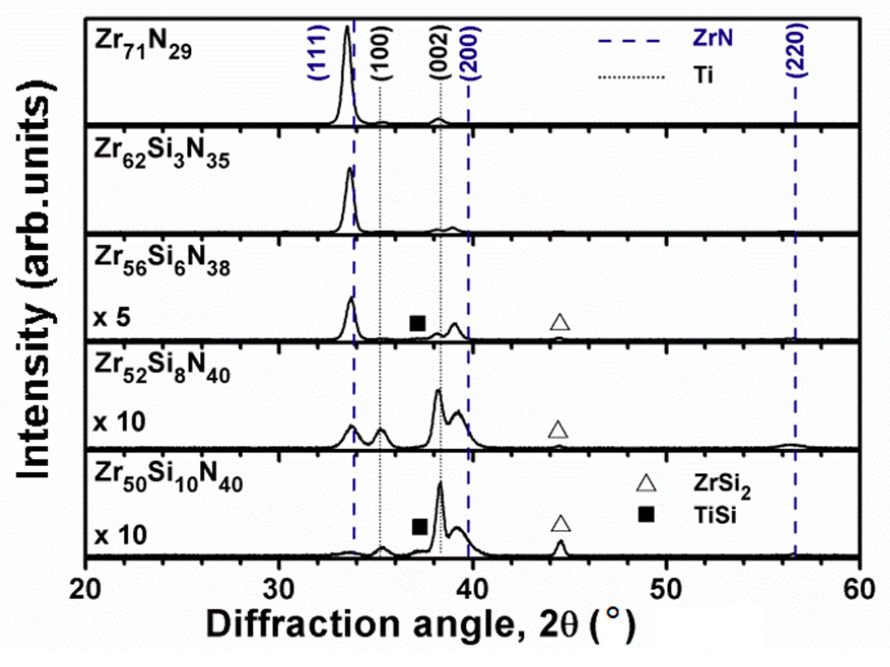
Figure 7.
Texture coefficients of Zr–Si–N films with various Si contents.
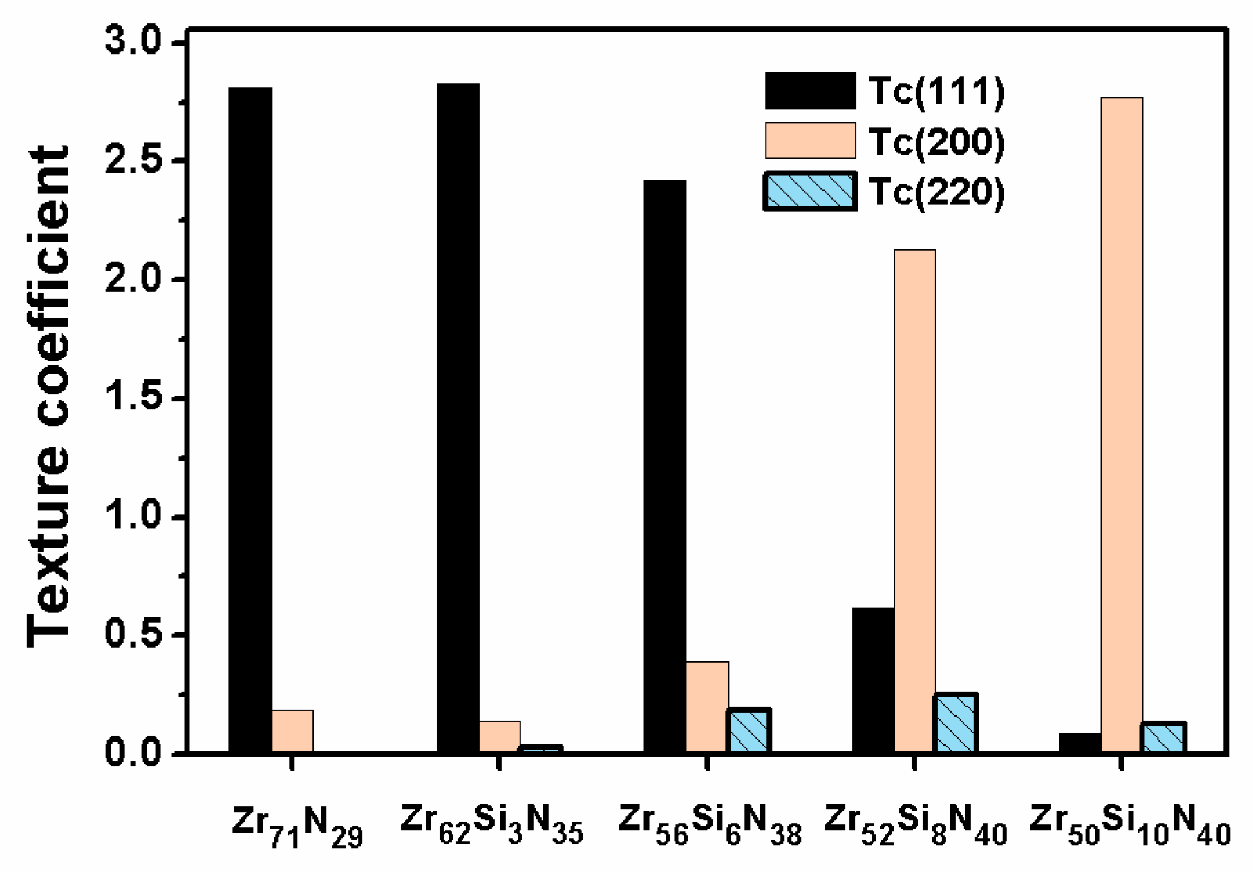
Figure 8.
Lattice parameters and grain sizes of the Zr–Si–N films.
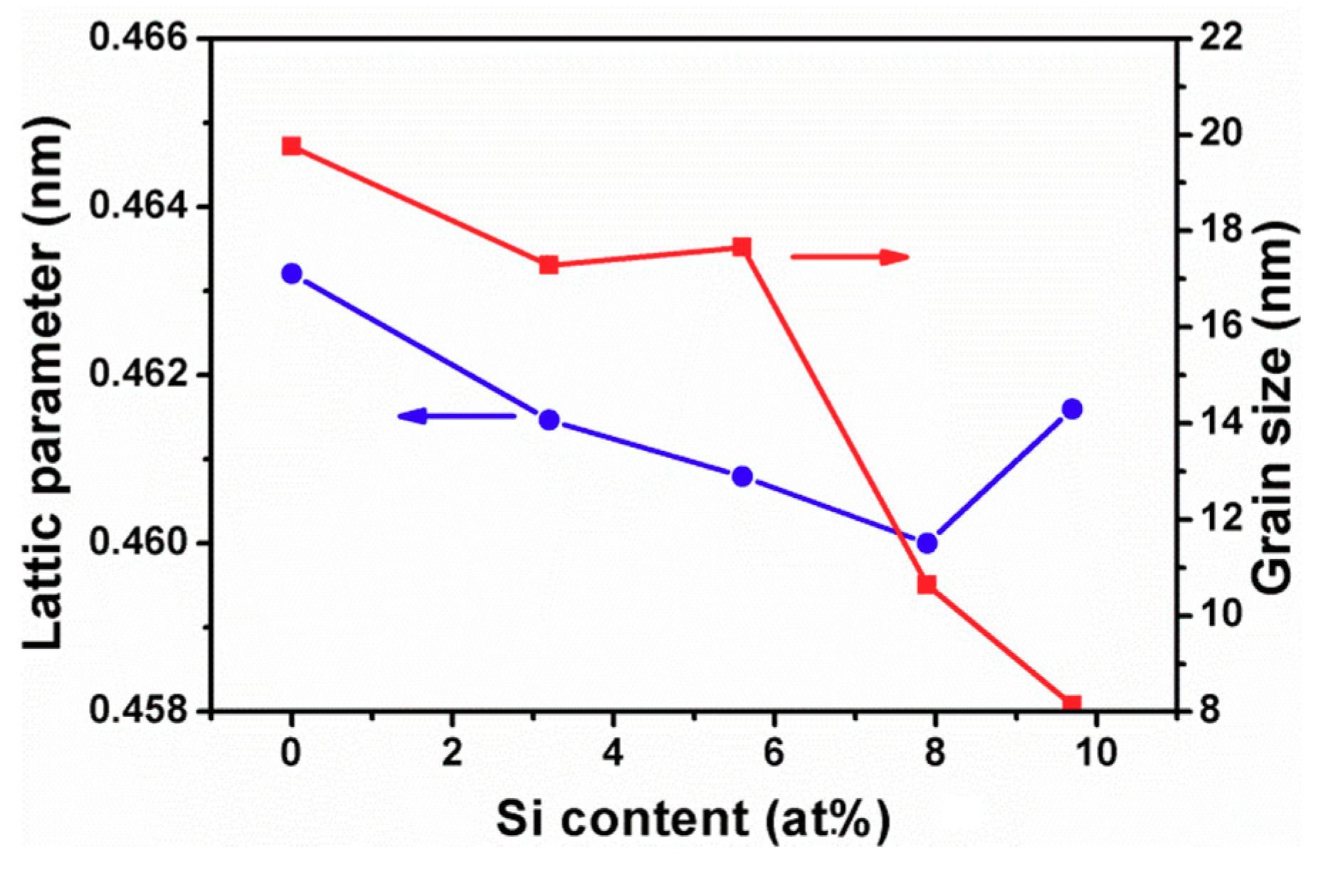
Figure 9.
(a) Cross-sectional transmission electron microscopy (TEM) image and selected area electron diffraction (SAED) pattern and (b) high-magnification TEM image of the Zr71N29 films.
Figure 9.
(a) Cross-sectional transmission electron microscopy (TEM) image and selected area electron diffraction (SAED) pattern and (b) high-magnification TEM image of the Zr71N29 films.
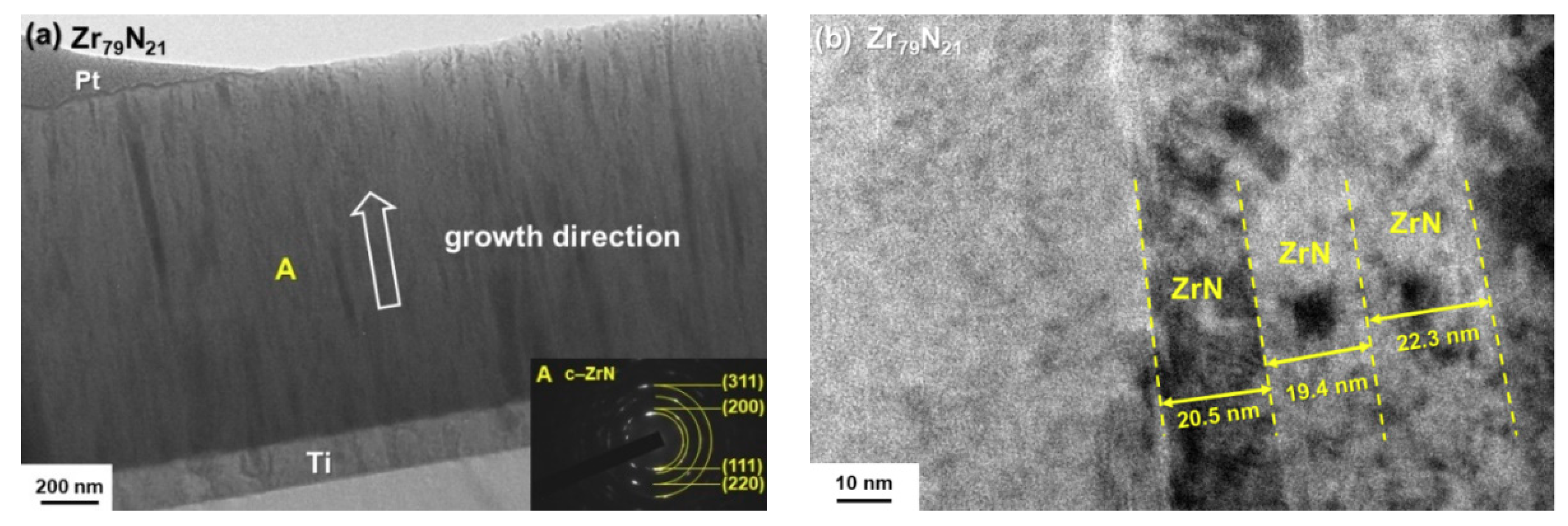
Figure 10.
(a) Cross-sectional TEM image and SAED pattern and (b) high-magnification TEM image of the Zr62Si3N35 films.
Figure 10.
(a) Cross-sectional TEM image and SAED pattern and (b) high-magnification TEM image of the Zr62Si3N35 films.
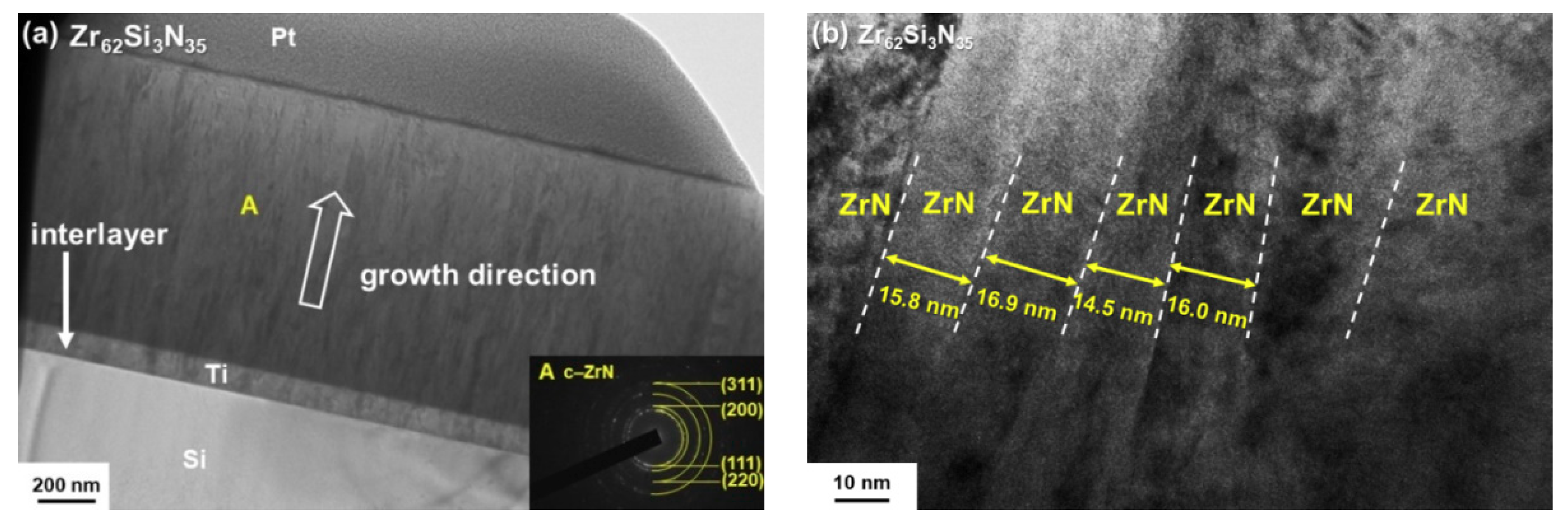
Figure 11.
(a) Cross-sectional TEM image and SAED pattern and (b) high-magnification TEM image of the Zr50Si10N40 films.
Figure 11.
(a) Cross-sectional TEM image and SAED pattern and (b) high-magnification TEM image of the Zr50Si10N40 films.
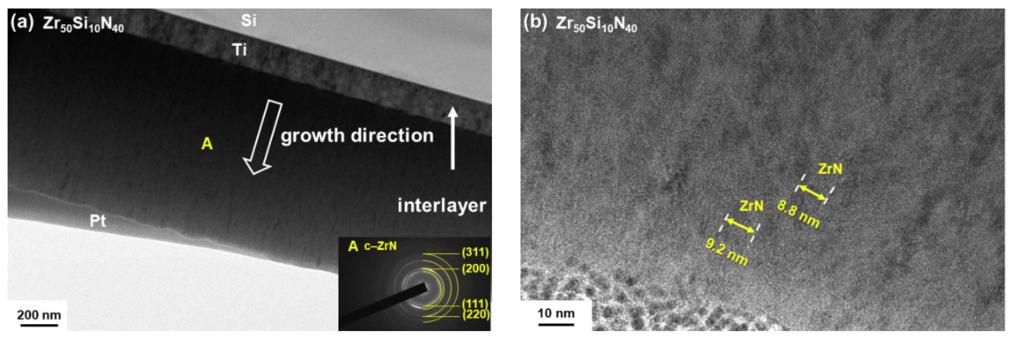
Figure 12.
Nanoindentation hardness and residual stress values of Zr–Si–N films.
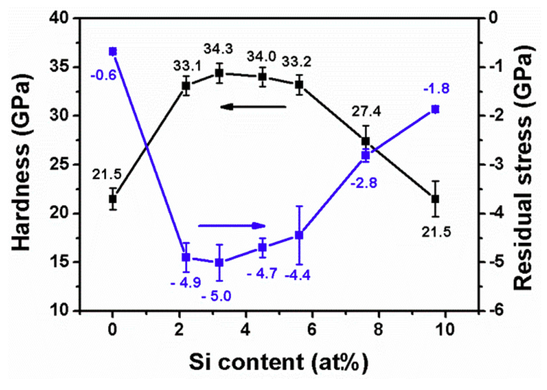
Figure 13.
The relationships of (a) nanoindentation hardness and (b) Young’s modulus of Zr–Si–N films to their residual stress values.
Figure 13.
The relationships of (a) nanoindentation hardness and (b) Young’s modulus of Zr–Si–N films to their residual stress values.


Table 1.
Sputtering parameters and thicknesses of Zr–Si–N films.
| Sample | Ar (sccm) | N2 (sccm) | HiPIMS PowerWZr (W) | RF PowerWSi (W) | Ave. Target Voltage (V) | Peak Current (A) | Time (min) | Thickness (nm) | Rate (nm/min) |
|---|---|---|---|---|---|---|---|---|---|
| Batch I | |||||||||
| Zr52Si8N40 | 28.0 | 2.0 | 300 | 50 | 660 | 67 | 210 | 831 | 4.0 |
| Zr48Si9N43 | 27.5 | 2.5 | 300 | 50 | 643 | 80 | 200 | 720 | 3.6 |
| Zr45Si10N45 | 27.0 | 3.0 | 300 | 50 | 600 | 90 | 240 | 732 | 3.0 |
| Zr44Si10N46 | 26.5 | 3.5 | 300 | 50 | 588 | 105 | 310 | 836 | 2.7 |
| Zr43Si10N47 | 26.0 | 4.0 | 300 | 50 | 588 | 110 | 360 | 898 | 2.5 |
| Batch II | |||||||||
| Zr71N29 | 28.0 | 2.0 | 300 | 0 | 640 | 58 | 400 | 1183 | 3.0 |
| Zr62Si2N36 | 28.0 | 2.0 | 300 | 25 | 618 | 67 | 285 | 937 | 3.3 |
| Zr62Si3N35 | 28.0 | 2.0 | 300 | 30 | 617 | 50 | 270 | 932 | 3.4 |
| Zr58Si5N37 | 28.0 | 2.0 | 300 | 35 | 615 | 70 | 255 | 926 | 3.6 |
| Zr56Si6N38 | 28.0 | 2.0 | 300 | 40 | 615 | 67 | 230 | 847 | 3.8 |
| Zr52Si8N40 | 28.0 | 2.0 | 300 | 50 | 660 | 67 | 210 | 831 | 4.0 |
| Zr50Si10N40 | 28.0 | 2.0 | 300 | 60 | 660 | 70 | 210 | 876 | 4.2 |
Table 2.
Chemical compositions, surface roughness, mechanical properties and residual stress values of Zr–Si–N films.
Table 2.
Chemical compositions, surface roughness, mechanical properties and residual stress values of Zr–Si–N films.
| Sample | Chemical Composition (at.%) | Ra (nm) | Ha (GPa) | Eb (GPa) | H3/E2 (GPa) | Stress c (GPa) | |||
|---|---|---|---|---|---|---|---|---|---|
| Zr | Si | N | O | ||||||
| Batch I | |||||||||
| Zr52Si8N40 | 52.0 ± 1.1 | 7.6 ± 0.2 | 40.1 ± 1.3 | 0.3 ± 0.1 | 3.5 ± 0.1 | 27.4 ± 1.6 | 256 ± 7 | 0.31 | −2.8 ± 0.1 |
| Zr48Si9N43 | 47.5 ± 0.7 | 9.0 ± 0.2 | 42.3 ± 0.9 | 1.2 ± 0.1 | 2.2 ± 0.2 | 20.4 ± 1.4 | 246 ± 9 | 0.14 | −1.6 ± 0.2 |
| Zr45Si10N45 | 44.6 ± 1.1 | 10.2 ± 0.2 | 44.4 ± 1.0 | 0.8 ± 0.2 | 0.3 ± 0.0 | 14.5 ± 0.2 | 184 ± 3 | 0.09 | −0.4 ± 0.1 |
| Zr44Si10N46 | 43.1 ± 1.3 | 10.1 ± 0.4 | 45.8 ± 1.3 | 1.0 ± 0.2 | 1.1 ± 0.1 | 13.8 ± 0.5 | 187 ± 7 | 0.08 | −0.2 ± 0.1 |
| Zr43Si10N47 | 42.4 ± 1.3 | 10.0 ± 0.2 | 46.6 ± 0.9 | 1.0 ± 0.3 | 1.1 ± 0.4 | 14.0 ± 0.6 | 190 ± 8 | 0.08 | −0.6 ± 0.1 |
| Batch II | |||||||||
| Zr71N29 | 70.6 ± 0.5 | 0.1 ± 0.0 | 28.7 ± 0.7 | 0.6 ± 0.2 | 4.4 ± 0.2 | 21.5 ± 1.1 | 283 ± 13 | 0.12 | −0.7 ± 0.1 |
| Zr62Si2N36 | 61.1 ± 1.9 | 2.2 ± 0.1 | 35.8 ± 2.1 | 0.9 ± 0.3 | 1.3 ± 0.2 | 33.1 ± 1.0 | 346 ± 11 | 0.30 | −4.9 ± 0.3 |
| Zr62Si3N35 | 61.0 ± 0.4 | 3.2 ± 0.1 | 34.9 ± 0.4 | 0.9 ± 0.2 | 1.4 ± 0.1 | 34.4 ± 1.0 | 369 ± 11 | 0.30 | −5.0 ± 0.4 |
| Zr58Si5N37 | 57.5 ± 0.2 | 4.5 ± 0.2 | 37.1 ± 0.1 | 0.9 ± 0.2 | 1.1 ± 0.0 | 34.0 ± 1.4 | 367 ± 13 | 0.29 | −4.7 ± 0.2 |
| Zr56Si6N38 | 55.8 ± 0.2 | 5.6 ± 0.1 | 37.9 ± 0.3 | 0.7 ± 0.2 | 0.8 ± 0.1 | 33.2 ± 1.0 | 373 ± 12 | 0.26 | −4.5 ± 0.6 |
| Zr52Si8N40 | 52.0 ± 1.1 | 7.6 ± 0.2 | 40.1 ± 1.3 | 0.3 ± 0.1 | 3.5 ± 0.1 | 27.4 ± 1.6 | 256 ± 7 | 0.31 | −2.8 ± 0.1 |
| Zr50Si10N40 | 49.9 ± 0.6 | 9.7 ± 0.1 | 40.2 ± 0.8 | 0.2 ± 0.3 | 3.3 ± 0.0 | 21.5 ± 1.8 | 230 ± 7 | 0.19 | −1.9 ± 0.1 |
a: Hardness; b: Young’s modulus; c: Residual stress.
© 2018 by the authors. Licensee MDPI, Basel, Switzerland. This article is an open access article distributed under the terms and conditions of the Creative Commons Attribution (CC BY) license (http://creativecommons.org/licenses/by/4.0/).
Share and Cite
MDPI and ACS Style
Chang, L.-C.; Zheng, Y.-Z.; Chen, Y.-I. Mechanical Properties of Zr–Si–N Films Fabricated through HiPIMS/RFMS Co-Sputtering. Coatings 2018, 8, 263. https://doi.org/10.3390/coatings8080263
AMA Style
Chang L-C, Zheng Y-Z, Chen Y-I. Mechanical Properties of Zr–Si–N Films Fabricated through HiPIMS/RFMS Co-Sputtering. Coatings. 2018; 8(8):263. https://doi.org/10.3390/coatings8080263
Chicago/Turabian StyleChang, Li-Chun, Yu-Zhe Zheng, and Yung-I Chen. 2018. "Mechanical Properties of Zr–Si–N Films Fabricated through HiPIMS/RFMS Co-Sputtering" Coatings 8, no. 8: 263. https://doi.org/10.3390/coatings8080263
Note that from the first issue of 2016, this journal uses article numbers instead of page numbers. See further details here.