Article

Combination of Zinc Oxide and Antimony Doped Tin Oxide Nanocoatings for Glazing Application

1
Fraunhofer IWS, Winterbergstrasse 28, D-01277 Dresden, Germany
2
King Abdulaziz City for Science and Technology KACST, P.O. Box 6086, Riyadh 11442, Saudi Arabia
*
Author to whom correspondence should be addressed.
Coatings 2018, 8(7), 248; https://doi.org/10.3390/coatings8070248
Submission received: 24 May 2018 / Revised: 10 July 2018 / Accepted: 10 July 2018 / Published: 12 July 2018
(This article belongs to the Special Issue Chemical Vapor Deposition 2018)

Abstract

:
Multilayered nanocoatings allow outstanding properties with broad potential for glazing applications. Here, we report on the development of a multilayer nanocoating for zinc oxide (ZnO) and antimony doped tin oxide (ATO). The combination of ZnO and ATO thin films with their promising optical properties is a cost-efficient alternative for the production of energy-efficient glazing. It is an effective modification of the building envelope to reduce current high domestic demand of electrical power for air conditioning, especially in hot climates like Saudi Arabia. In this paper, we report the development of a nanocoating based on the combination of ZnO and ATO. Principle material and film investigations were carried out on lab-scale by dip coating with chemical solution deposition (CSD), while with regard to production processes, chemical vapor deposition (CVD) processes were evaluated in a second stage of the film development. It was found that with both processes, high-quality thin films and multilayer coatings with outstanding optical properties can be prepared. While keeping the optical transmission in the visible range at around 80%, only 10% of the NIR (near infrared) and below 1% of UV (ultraviolet) light passes these coatings. However, in contrast to CSD, the CVD process allows a free combination of the multilayer film sequence, which is of high relevance for production processes. Furthermore, it can be potentially integrated in float glass production lines.

1. Introduction

The application of suitable glazing is an effective modification of the building envelope to reduce current high domestic demand of electrical power for air conditioning, especially in hot climates like Saudi Arabia [1,2]. Besides applying vacuum glazing and aerogel filling material, multilayer coatings are of special interest [3,4]. As glass materials used for ordinary fenestration exhibit high transparency in the solar range (300–2500 nm), wavelength-selective light transmission is one key feature addressed by these kinds of nanocoatings. In order to reduce the transmission of UV and IR (infrared) radiation, these coatings have to be designed to be transparent in the visible range (380–780 nm). Especially in hot climate regions, the IR radiation contributes to 53% of the heat being transferred inside buildings connected with the electric power demand for air conditioning [5,6]. Furthermore, the short wavelength UV radiation is responsible for furniture bleaching and decompositions at the interior surfaces. Efficient solutions for blocking these radiations while remaining transparent for visible light are desired. Typically, multilayer coatings based on silver or nickel embedded in a stack of oxidic or sulfidic support layers are used to obtain this effect [7,8] These layers are very effective, but have to be applied by costly vacuum deposition methods. Furthermore, thermochromic or electrochromic coatings based on tungsten oxide are used to realize so-called smart glazing [9]. The idea of these coatings is self-regulation of the light transmission by phase changes inside the material resulting in a darkening of the windows under high irradiation. While a darkening effect can be generated and tuned quite well depending on the amount of irradiated light, wavelength-selectivity is hard to adjust.
In contrast to these approaches, semiconductive materials with bandgaps >3 eV exhibit sufficient high transparency in the visible range. The reduction of solar radiation, especially in the IR region, can be influenced by dopants to achieve transparent conductive oxide (TCO) materials with reflective properties in the NIR range (780–2500 nm) [10,11]. Moreover, in the UV range (<380 nm), suitable semi-conductive materials can contribute to reducing the solar transmission.
In this work, we combine two semi-conductor based thin film hard coatings in order to achieve efficient solar control glazing. We focus on cost-efficient materials and processes. The concept is based on a double layer setup with one UV-blocking and one NIR-blocking layer. The UV absorbing layer consists of zinc oxide (ZnO). This material offers a sharp absorption edge at 380 nm because of distinct electronic transitions taking place exactly below the boundary line between the UV and the visible part of the light [12]. Thus, it is a good candidate for efficient UV-blocking. The IR-blocking coating selected for this study is antimony doped tin oxide (ATO). This TCO material exhibits a plasmon resonance in the NIR range, and thus causes IR reflectivity [13]. The proposed coating could be applied, for example, on the vacuum gap facing side of an outer sheet of a double glazing setup.
Besides the optical properties of the combined nanocoatings, the process development for the film deposition is the focus of this work. While for general studies on the concept, a coating layout is carried out in simple lab-scale chemical solution deposition (CSD) processes by dip coating, in this case, production-relevant processing by chemical vapor deposition (CVD) was evaluated for final film optimization. These two processes are of high interest for both laboratory sample preparation and industrial scale film deposition. Particularly in terms of cost-efficient glazing production, the utilized aerosol-assisted CVD process at atmospheric pressure provides the ability to be competitive with state-of-the art vacuum-based physical vapor deposition (PVD) processes [14].

2. Materials and Methods

Thin films were prepared by chemical solution deposition (CSD) and chemical vapor deposition (CVD) methods on 1.1 mm thick C1737 glass from Delta Technologies (Loveland, CO, USA).
For CSD, being a generic term for different deposition methods using precursor solutions, we used the dip coating plus annealing method from the following precursors: Zinc oxide thin films were deposited on C1737 substrates from a solution as reported by Ohyama et al. [15] with 16.463 g zinc acetate dihydrate (99.8% Alfa Aesar, Karlsruhe, Germany) in 100 mL of 2-Methoxyethanol (99% Sigma Aldrich, Taufkirchen, Germany), with 4.581 g of 2-Aminoethan-1-ol (99.5% Sigma Aldrich), was used. Using multiple dip coating steps with 1 mm/s and subsequent drying and heating in air at temperatures between 300 and 600 °C, compact films with different film thicknesses and crystallinity were obtained.
Antimony doped tin oxide films were prepared in a similar manner by applying a solution reported by Aegerter et al. [16] containing 3.792 g tin (II) chloride (99.9% Alfa Aesar), 50 mL abs. ethanol, and the desired volume of a 0.5 M antimony (III) chloride (99.9% Alfa Aesar) solution in ethanol and 4.646 g of 4-Hydroxy-4-methylpentan-2-one (99% Sigma Aldrich) in order to realize initial Sb/Sn ratios between 0 and 15% in the solution. The films were annealed in air at 600 °C for 15 min, if not stated otherwise.
For CVD of ZnO and ATO, an aerosol-assisted process and equipment was used, as we reported earlier [17]. The following precursor solutions were used: For ZnO films, 40 g zinc acetate dihydrate (99.8% Sigma Aldrich) was dissolved in 200 mL deionized water; 26.05 g of tin tetrachloride (99.9% Alfa Aesar) was dissolved in 270 mL absolute ethanol. Antimony trichloride was added in amounts between 0 and 3.422 g in order to adjust the Sb/Sn ratio between 0 and 15%. If not stated otherwise, a 360-nm coating (12 runs) of ZnO was used as sublayer for combined ZnO/ATO CVD coatings.
As-prepared thin films were characterized through the following methods: The optical properties of the films were measured by total transmittance and reflectance measurements using a UV-visible (VIS)-NIR (0.3–2.5 μm) spectrophotometer (Perkin Elmer, Rodgau, Germany; Lambda 900 with 150 mm integrated sphere), a Fourier transform (FT)-IR (1.7–20 μm) spectrophotometer (Perkin Elmer, Spectrum 2000 with Pike integrated sphere “IntegratIR”), and a spectroscopic ellipsometer (J.A. Woollam Co., Darmstadt, Germany; VASE; indices of refraction were evaluated at 550 nm). The structural properties were investigated by X-ray diffractometer (XRD, X´Pert Pro from Panalytical, Kassel, Germany; Cu-Kα-radiation (λ = 1.5405 Å)) and a scanning electron microscope (SEM, ZEISS GeminiSEM 500, Jena, Germany).
For evaluating τ-values of the coatings, C1737 spectra were used as reference, while air was used as reference for the uncoated C1737 glass.

3. Results and Discussion

3.1. Film Development by CSD

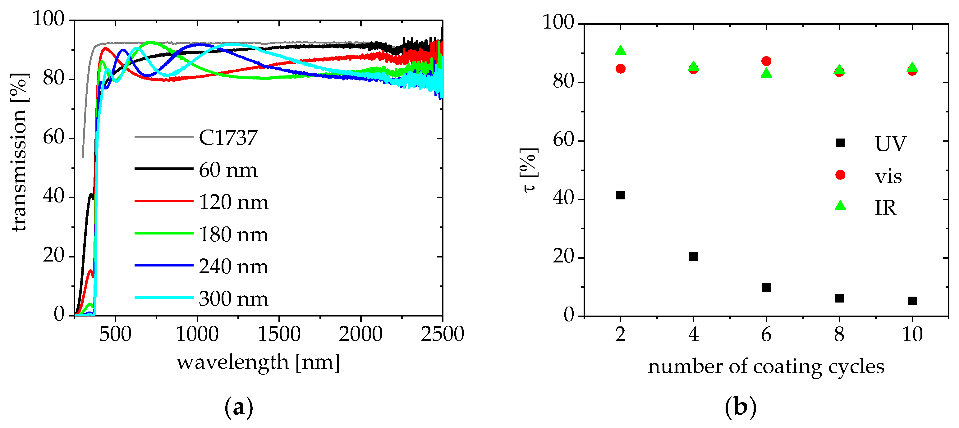
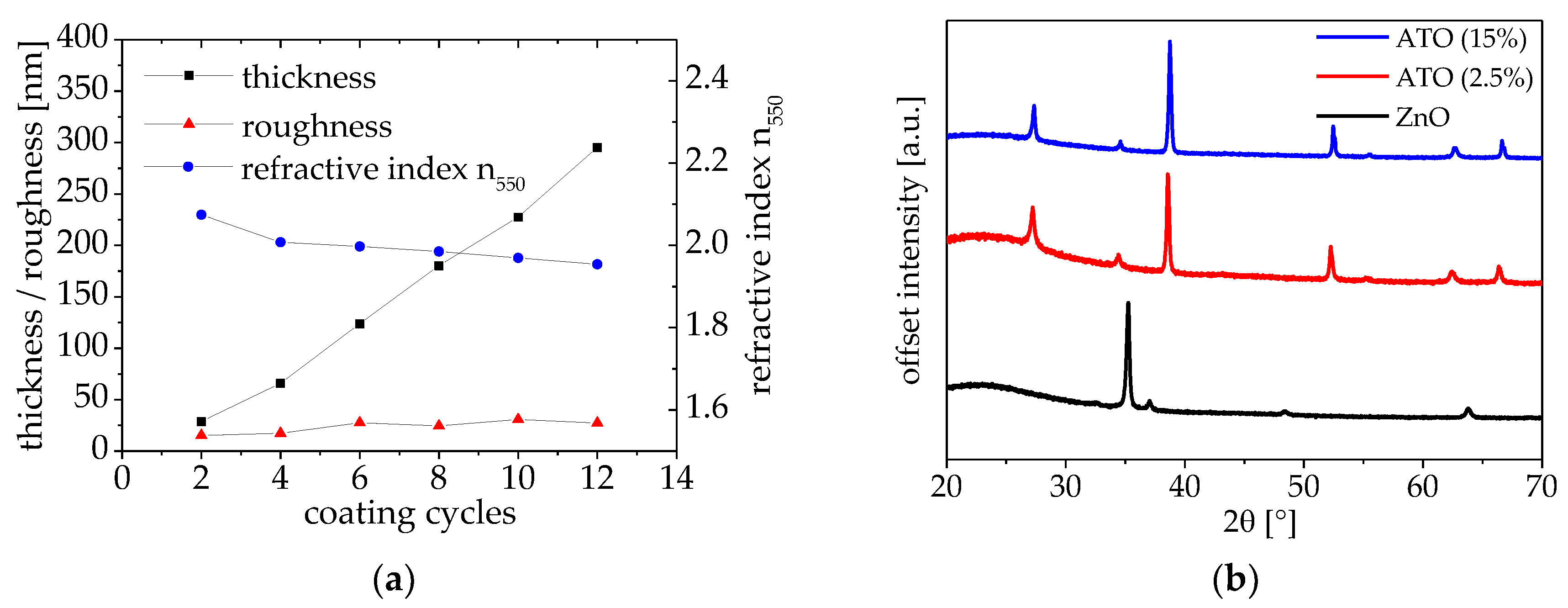
3.1.1. Zinc Oxide Films by CSD

For a reasonable utilization of the zinc oxide‘s UV absorption properties, a minimum crystallinity of the thin films is expected to be required. Therefore, XRD investigations were carried out from dip coated samples with comparable film thickness (derived from ellipsometry data: ~90–100 nm ZnO on each side of the glass substrate) annealed at different temperatures. From Figure 1, it can be seen that crystalline phases can be detected for films with annealing temperatures of 400 °C and above. Besides ZnO, no side phases could be detected [18]. The crystallinity increases with the annealing temperature, because the intensity of the reflection peaks—or more precisely their full width at half maximum—increases in this manner.
The optical transmission spectra of these samples exhibit a distinct absorption edge at 380 nm, as is expected for ZnO. However, the different shape of the shoulder at 345 nm indicates a different quality in the absorption behavior, as it is attributed to the superposition of ZnO absorption and glass substrate absorption. While for samples prepared at 500 °C and 600 °C, the shoulder is well pronounced, for the 400 °C sample, the shoulder exhibits less sharpness. In contrast to the higher temperatures, incomplete precursor decomposition may affect the optical behaviour. Carbon impurities could be one reason for this observation. At even lower annealing temperatures (300 °C), there is no clear differentiation of the shoulder. Consequently, the best optical performance in terms of absorption is obtained for tempering at 500 °C and above. However, when comparing the transmission of the samples prepared at 500 °C and 600 °C, it is very clear that the 500 °C sample offers higher transmission, which can be attributed to the somewhat lower index of refraction of this sample (n550 nm = 1.81 at 500 °C vs. n550 nm = 1.94 at 600 °C). Thus, a thermal annealing at 500 °C should be considered as optimum conditions in terms of optical properties of the dip coated ZnO films.
Because the observation of a shoulder in the transmission spectra between 250 nm and 380 nm indicates an incomplete absorption below 380 nm, the optimization of the ZnO film thickness is a necessary step for film development. Therefore, ZnO films with different film thicknesses were prepared by CSD via multiple dip coating and annealing steps (each performed at 500 °C). From the optical transmission spectra, it can be seen that the shoulder is still present even at film thicknesses of 180 nm.
We use the τ-value in order to simplify the optical transmission properties of a sample. Therefore, the transmission T of a sample is integrated in a certain wavelength range (UV: λ1 = 250 nm and λ2 = 380 nm; VIS: λ1 = 380 nm and λ2 = 780 nm; NIR: λ1 = 780 nm and λ2 = 2500 nm) with regard to the transmission of a reference TRef. While for the uncoated C1737 film, transmission in air was used as reference, for the coated samples, the transmission was referenced against the C1737 glass. Thus, the τ-value is a measure for the overall light transmission in a certain wavelength range.
τ λ 1 , 2 =   λ 1 λ 2 T Ref ( λ ) T ( λ ) d λ λ 1 λ 2 T Ref ( λ ) d λ  
According to Equation (1), a 360-nm and a 500-nm thick film transmits only 0.9% and 0.01% of the UV light, respectively (see Figure 2). The reduced transmission in the visible and NIR range are mainly due to interference losses caused by relatively high indices of refraction (n550) of 1.8–2.0. However, the τ-values of the ZnO samples in the visible and NIR-range are around 80% and higher, indicating that the films are quite transparent in these ranges. Thus, different ZnO film thicknesses only have minor influence on the τ-values for visible and NIR light.
Consequently, in order to have an efficient UV-blocking layer, ZnO film thicknesses of at least around 350 nm should be applied. The solution-based preparation of highly visible light transparent and UV-blocking ZnO layers should be thus carried out at 500 °C and with film thicknesses >350 nm.

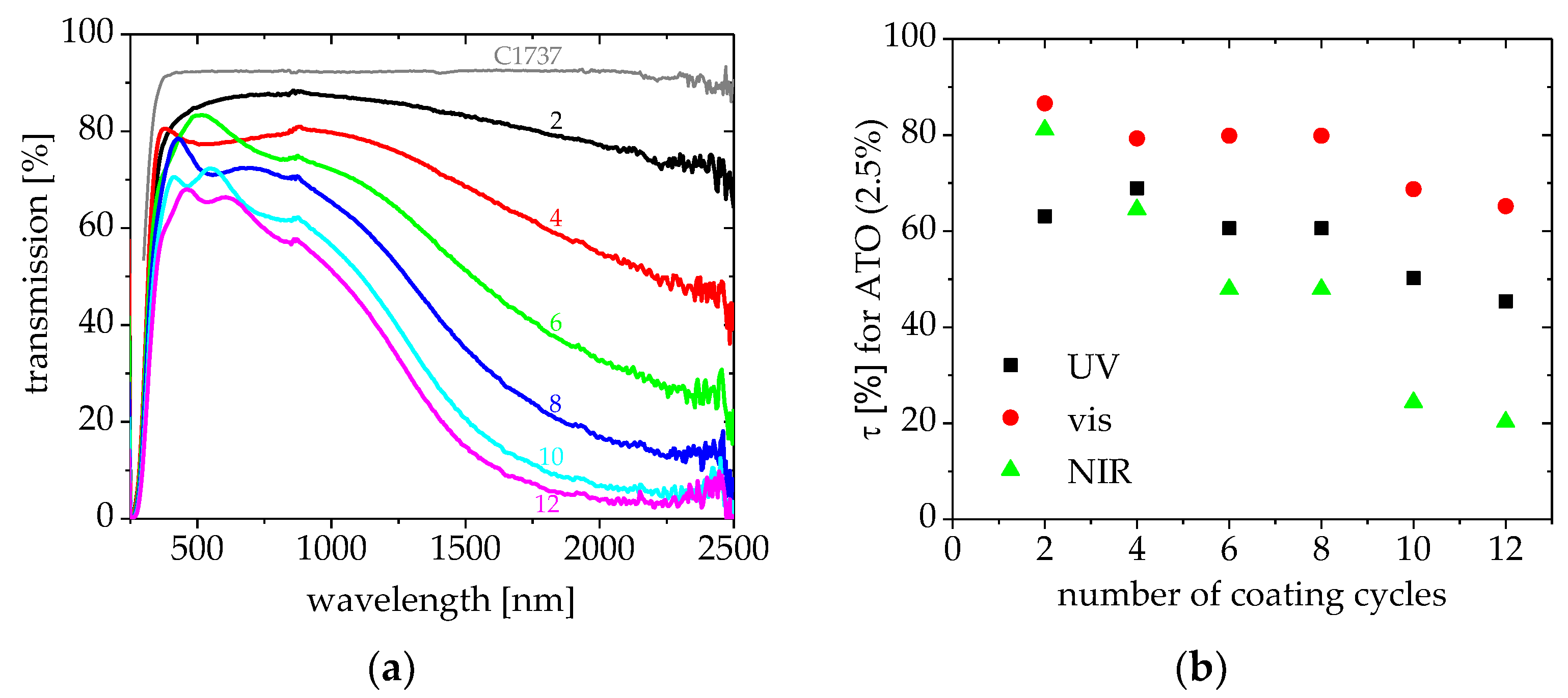
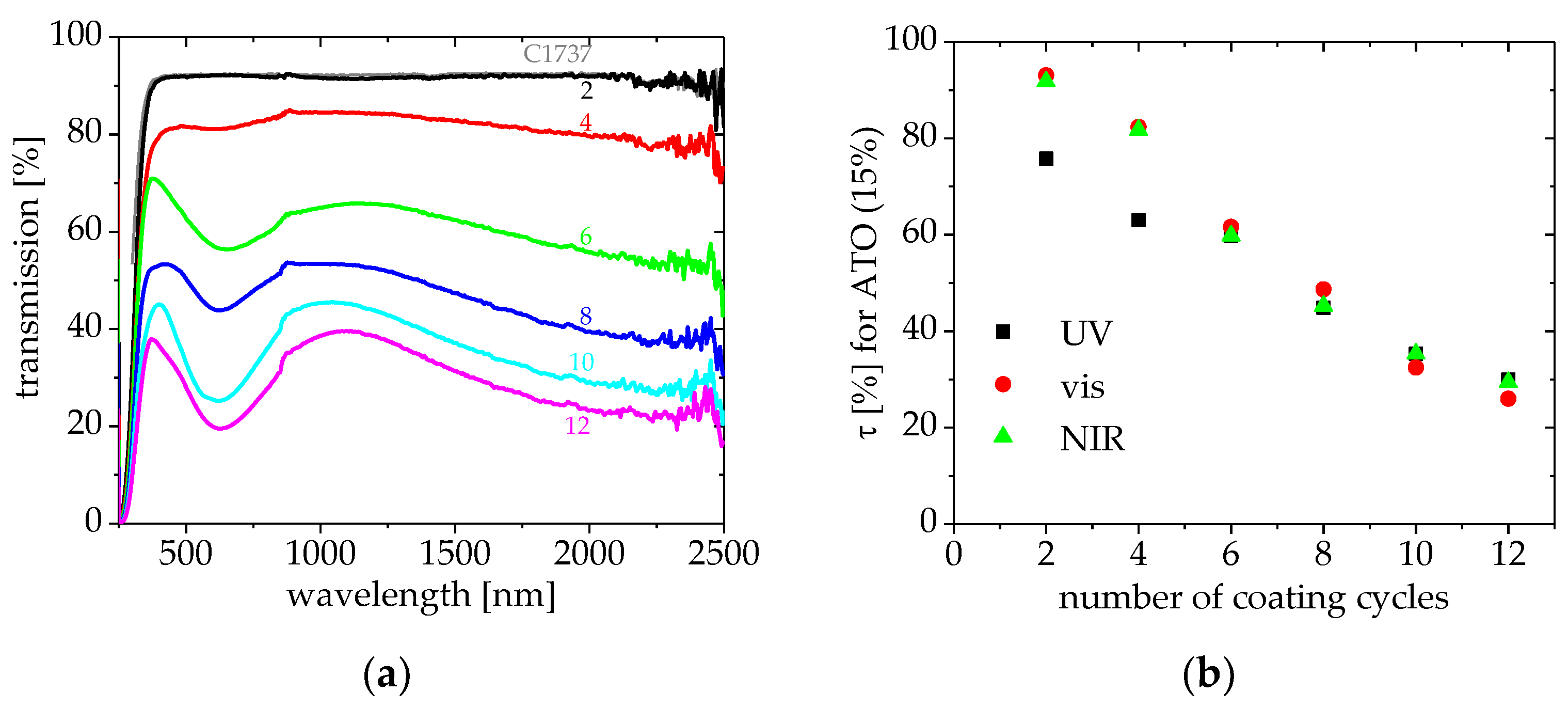
3.1.2. ATO Films by CSD

Similar to ZnO film optimization, the ATO layer was also individually optimized. Therefore, the influence of antimony content in the precursor solution was evaluated in the first step. Dip coated samples with thicknesses in the range of 110–150 nm were prepared. The main differences in the spectra were found in the range 1000–2500 nm, while the influence in the UV and visible range is much lower. Regarding the optical behavior in the NIR region, it could be found that up until a Sb/Sn ratio of 12.5%, the transmission decreases (see Figure 3a). There is no strong influence observed for higher antimony contents: The samples with doping levels in the range 7.5–17.5% have almost equal spectral transmission behavior. The slightly thinner sample prepared with 17.5% doping level has a slightly higher transmission compared with the 12.5% doping level, which may be mainly due to the different film thicknesses. Thus, an intermediate doping level of 10% Sb in the ATO precursor was chosen for further experiments. This doping level results in efficient IR reflection properties, as can be seen from Figure 3b. However, also in the visible light range, the transmission was slightly influenced. This effect seems to be dominated by the film thickness. To evaluate the influence of ATO film thickness, and in order to improve the IR-blocking behavior of the films, ATO coatings with different film thicknesses have been prepared by multiple dip coating steps. Increasing film thicknesses mainly affects the optical behavior in the IR range, while having only a small influence on the visible region and almost no influence on the UV region. Compared with the uncoated glass reference, an ATO layer thickness of 500 nm results in a τ-value of 99.8% for the UV light, 70.3% for visible light, and the τ-value for IR light is found to be 10.7%, as can be derived from Figure 3. With increasing coating thicknesses of 25, 180, and 260 nm, the τ-values in the IR decrease from 82% to 53% and 36%, respectively. This behavior allows the tuning of the IR transmission behavior in the 780–2500 nm range, while the UV and visible transmission is only slightly affected.
The optical transmission is mainly influenced by the optical constants (dielectric function) and the amount of charge carriers. A series of samples with different thicknesses was prepared at 600 °C from solutions with a 10% initial doping level by multiple dip coating cycles. These samples were evaluated by ellipsometry in order to obtain thickness information and the index of refraction. From Figure 4a, it can be seen that the thickness of the coating increases linearly with the number of cycles. The index of refraction also increases linearly for films with thicknesses below 120 nm. This may be due to the dominant influence of the substrate on defect density, crystallite size, and orientation for low film thicknesses. Above 120-nm, the index of refraction remains more or less constant, as bulk properties are reached for these thicker films.
The films’ sheet resistance is also strongly dependent on the film thickness, as can be seen from Figure 4b. With increasing thickness, the sheet resistance decreases by orders of magnitude. Sheet resistances of ~100 Ω can be realized for film thicknesses above 150 nm. The specific resistance shows some small thickness dependence at low film thicknesses, but levels at a constant value of ~5 × 10⁻⁵ Ω∙m for thicknesses above 30 nm. The electric properties are strongly connected with IR reflection. This finding is in agreement with the optical data, as a highly conductive film will also offer good IR-blocking behavior.

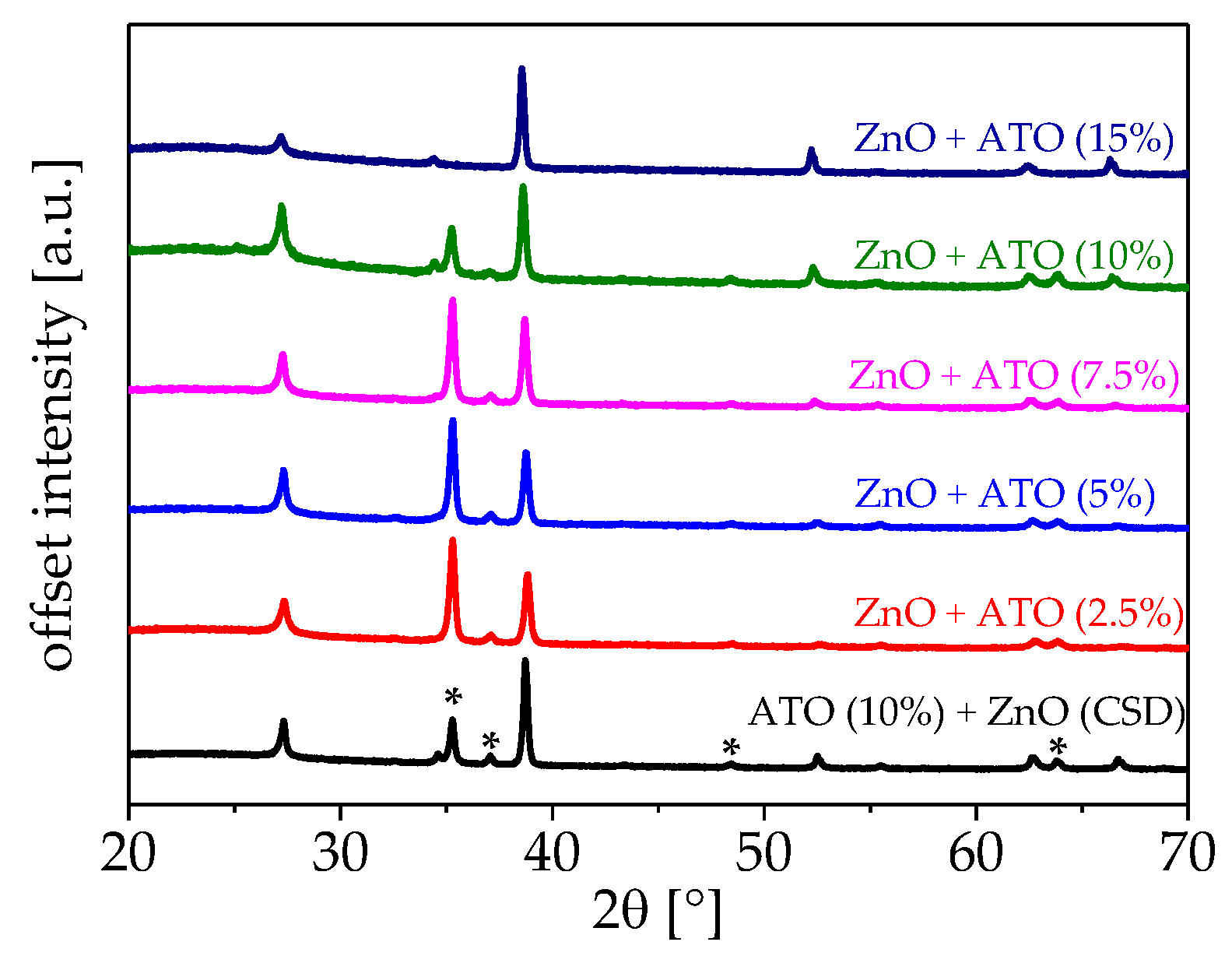
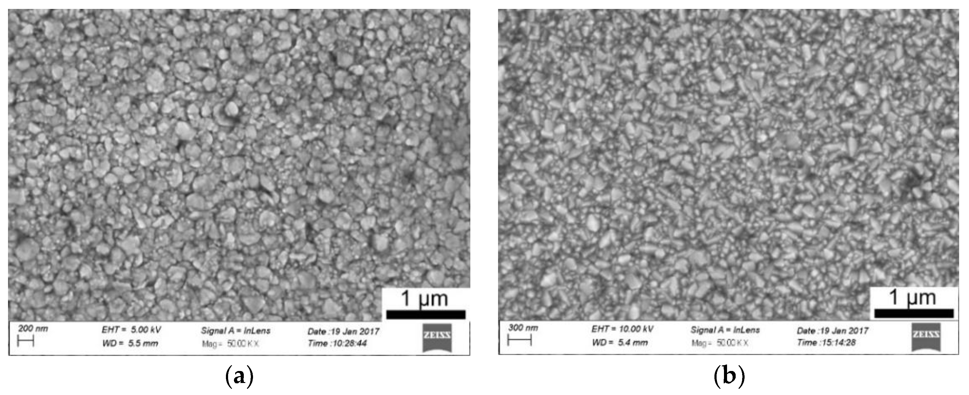
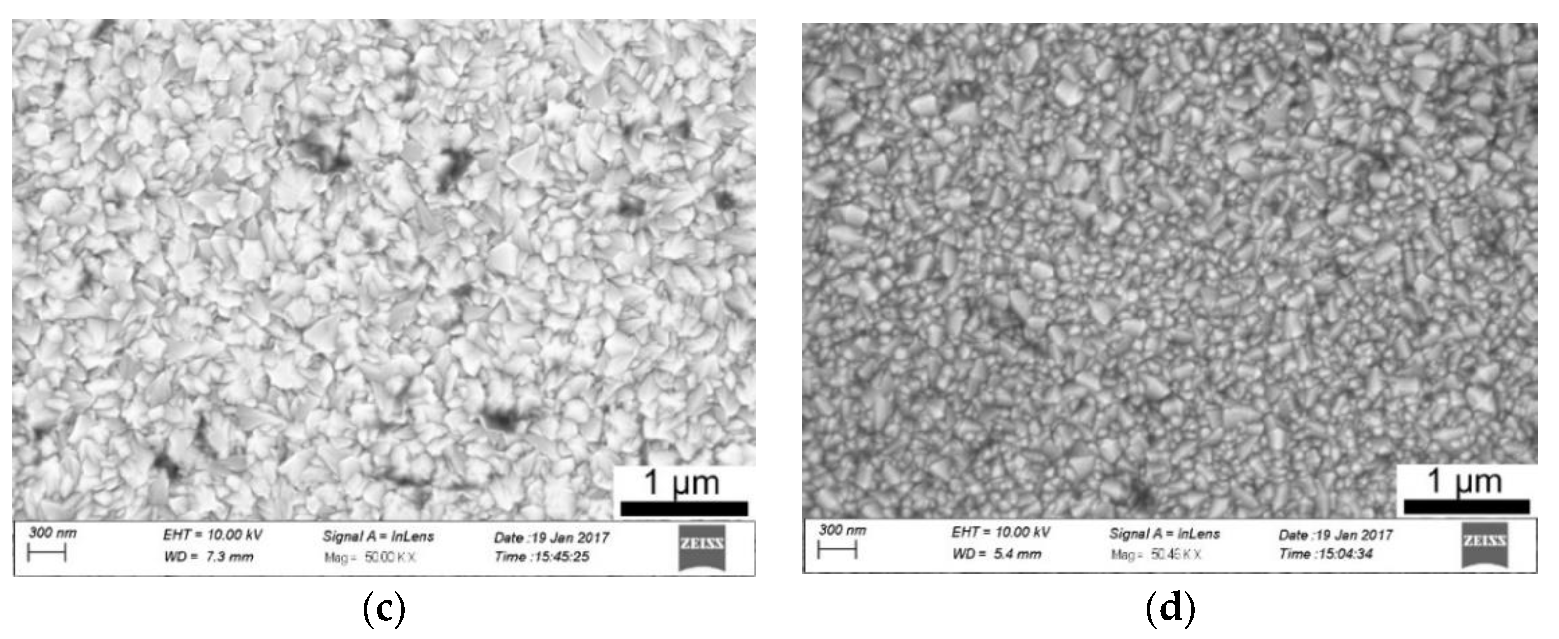
3.1.3. Combination of ATO and ZnO Films by CSD

Because both films ZnO and ATO exhibit only a small influence on the visible region, a combination of both films was expected to provide UV-blocking and IR-reflecting properties, while being relatively transparent in the visible region.
ATO layers were deposited on top of ZnO coated glass by dip coating. As can be seen from Figure 5, this sequence of coating steps leads to the loss of UV-blocking properties. This is because of the acidic properties of the ATO precursor. By dipping the ZnO coated substrate into the ATO precursor solution, ZnO is etched away, and thus the coating loses its UV-blocking properties. This might be avoided by using different ATO precursor solutions with lower acidity. However, the chloride based precursors salts are the most cost-efficient antimony and tin sources (besides the oxides themselves), leaving not much room for alternatives. Consequently, a combination of ZnO and ATO by CSD is only achievable by coating ZnO on top of ATO. Figure 5 shows that this sequence exhibits the desired UV-blocking/IR-reflecting properties. A combination of these nanocoatings can thus be used for efficient solar control glazing. However, as this experiment shows, a ZnO topping layer cannot be favored in terms of chemical stability. It is much more preferable to have the tin oxide-based, and thus chemically relatively well resistant, ATO as an outer layer. Based on these lab-scale investigations, we investigated CVD processes for evaluating the flexibility in the deposition sequence for these processes. Because CVD is potentially better to scale and might be designed to be implemented in float glass production lines, its practical relevance offers another reason for its consideration for glazing development.

3.2. Application of CVD Processes

3.2.1. Single Layer Deposition by CVD

In order to avoid wet-chemical etching of ZnO layers, a dry vapor-based CVD process was used to realize the desired coatings. Similar to the CSD process, different film thicknesses of ZnO and ATO were realized in order to be able to tune the optical properties of double layers in the subsequent steps. While the ATO film deposition by CVD is described elsewhere in our previous work [17], the ZnO deposition by CVD was of special interest. Again, the ZnO film thickness was evaluated in order to realize a >99% absorption of UV light. According to Figure 6, this was achieved for film thicknesses >240 nm. The τ-value for the UV range decreases with the number of coating cycles, and thus with the film thickness, while the visible and NIR-transmission remains unaffected by the film thickness. As losses in the latter ranges are only due to interferences, the films’ optical quality is considered to be very high with low impurities.
The direct influence on the optical behavior of the ZnO films, especially in the UV range, is a result of the increasing film thickness with the number of coating cycles and because of different refractive indices. While with the number of coating cycles the film thickness increases more or less linearly, with approximately 25–30 nm per cycle; the refractive index decreases from 2.09 for 30-nm thick films to 1.96 for 300-nm thick films. The latter might be because of a slight change in crystal sizes or grain orientation for the thicker films. This goes along with a slightly increased roughness of thicker films, as obtained from ellipsometry measurements, because a larger crystal size leads to a higher roughness and a higher tendency for preferred orientation. Opposing crystal faces from neighbored grains need to have similar orientation in the case of large grains in order to allow relatively defect-free film growth. Otherwise, pinhole formation would be the result. From Figure 7b, a preferred orientation of the ZnO film prepared at 500 °C can be seen. XRD patterns of ATO layers from both 2.5% and 15% initial doping levels show the formation of a phase pure ATO films—no side phases were detected even for the high doping amounts [19,20]. Consequently, the Sb atoms are efficiently incorporated into the SnO2 lattice.
As expected, a strong relation of the optical behavior of ATO films prepared by CVD with the film thickness and doping level could be found (see Figure 8 and Figure 9). While for low doping levels, mainly the IR range can be influenced; for high doping levels, IR, visible, and UV ranges are influenced. This blackening for heavily Sb doped tin oxide is in accordance with observations by Kojima et al. [21]. However, efficient UV-blocking cannot be obtained with just ATO coatings.

3.2.2. Combination of ZnO and ATO Films by CVD

With the CVD process, it was possible to deposit ATO on top of ZnO. Because the ATO precursor is vaporized on the surface of the ZnO coated substrate, etching does not occur. This can be seen from the XRD measurements shown in Figure 10. In all multilayer samples, the main reflection peaks at 35.3° for ZnO and 37.0° can be found simultaneously with the main reflections for SnO2 at 27.2°, 34.4° and 38.6°. Consequently, the CVD process can be used to produce the preferred film sequence with ATO on top of ZnO, which is not possible with the described CSD routine. As can also be seen from Figure 10, the growth of the ATO layer depends on the doping level. Different intensities of the main reflection peaks can be found for different doping levels. This may be mainly affected by the resulting dominant surface crystal faces and crystallite orientation. Moreover, a higher antimony content widens the tin oxide lattice, which results in a slight shift of the reflection to smaller angles.
For the preparation of the double layer nanocoating samples discussed in the following section, a C1737 substrate coated with approximately 360-nm ZnO (12 runs) was used. While the ZnO parameters were kept constant, ATO doping level and film thicknesses were varied in these investigations.
The microstructural appearance of the CVD films seems to be only slightly influenced by the precursor or film composition. ZnO and ATO/ZnO combinations show similar crystal shape and size. Figure 11 shows a homogeneous and dense surface for each film or combination. A slight tendency towards smaller crystal sizes can be observed with increasing Sb doping levels. This could be because of the higher amount of defects introduced at higher doping levels, as these would act as nucleation sites for new crystallites.
Besides XRD, also from optical measurements, the presence of the ZnO layer could be observed after ATO deposition. This can be seen from the efficient UV-blocking behavior of all double layer samples. The effect of the ATO thickness and doping level is similar to that of the ATO single layers. Thus, it is possible to realize a nanocoating offering 50% NIR-blocking at 80% visible light transmission and with almost 100% UV-blocking (see Figure 12).
Moreover, if a 15% initial doping level is used for ATO deposition on ZnO, the visible and NIR light is blocked by similar percentages. While full UV-blocking is observed, no selectivity for either the visible or NIR range can be observed. The heavy doping causes visible light absorption, and thus loses the advantage of selective light transmission. According to Figure 13b, the τ-values of these coatings decrease in a similar manner. Thus, only a film thickness effect according to Beer’s law is observed in the visible and NIR range. However, these films still offer application potential for glazing since visible light protection may also be of interest for regions with outstanding high solar irradiation.
The used CVD method utilizes atmospheric pressure equipment. Furthermore, it makes use of relatively cost-efficient raw materials. An integration into float glass production lines thus may potentially offer a clear advantage over conventional vacuum-based processes. Consequently, the described process has great potential for prize-competitive functional solar control coatings, and thus for affordable glazing in this mass market segment.

3.3. Comparison of CVD and CSD

With both of the used techniques, CVD and CSD, high-quality thin film preparation could be carried out. However, each technology has advantages over the other, depending on the respective focus. Comparing the optical properties of the prepared ZnO films, it seems that CVD has a slight advantage over CSD. Especially when comparing ZnO spectra from CSD (Figure 2a) and CVD (Figure 6a), it can be seen that for the CVD samples, only the absorption in the UV is changing with the film thickness, while the visible and NIR regions are only influenced by interference effects. All transmission spectra exhibit no transmission loss higher than 10% in this range compared with C1737. In contrast to that, spectra of samples prepared by CSD exhibit up to 20% transmission loss at certain wavelengths, especially in the visible region. This may be because of the higher amount of organic ingredients, which, if not fully decomposed, can cause carbon impurities and thus visible light absorption. The CVD precursor is on aqueous base, and thus less carbon may be formed. Besides this, CSD is a very versatile technology especially for small sample preparation without a high effort for equipment or infrastructure. Furthermore, CSD offers very high precursor yield, which is not the case for CVD. Both methods are scalable to large formats of a few meter sample widths, and are thus applicable for industrial processes. Because CVD would allow integration in float glass lines, an in-situ deposition of the coating on the still hot glass sheets can be carried out. No additional heating or annealing would be needed, which would be the case for CSD processes.
The main disadvantage of CSD for the specific thin film system described in this work becomes obvious from the results in Section 3.1.2. The deposit of the preferred layer sequence could not be realized. The chemically and mechanically more resistant tin oxide based ATO layer would preferably be deposited on top of ZnO, which is not possible as the ATO precursor solution etches the ZnO. With CVD, the ATO precursor vaporizes over the sample surface avoiding an etchant contact with the sensitive ZnO. Thus, an ATO deposition on top of ZnO is possible.

4. Conclusions

The results from this work clearly show the possibility of combining ATO and ZnO layers in order to achieve high-quality coatings for solar control glazing. With both investigated deposition methods, solution-based CSD and vapor-based CVD, it is possible to prepare highly UV- and IR-blocking layers, while keeping visible light transmission high. However, while the CSD method is rather useful for process development, it offers drawbacks in terms of practical relevance. The preferred film sequence of ATO forming a chemically resistant protective layer on top of ZnO could not achieved by this method. With the described double layer ZnO/ATO approach, it was possible to realize a CVD coating offering a 99% UV-blocking and up to 60% NIR-blocking, while enabling ~80% of visible light transmission through the coated glass at the same time. Furthermore, it could be demonstrated that the optical properties of the coatings can be nicely tuned by the precursor and deposition parameters. Especially, the ATO layer allows both NIR and visible light transmission tuning by adjusting the antimony content. By applying a >240-nm thick ZnO coating a glazing with >99% UV light blocking properties can be realized.
By applying the described coatings to window glass sheets, an energy- and cost-efficient alternative to existing thermal control glazing solutions may become possible.

Author Contributions

Conceptualization, B.S., T.A., and H.A.; Methodology, B.S., T.H. and H.A.; Investigation, T.A., B.S., P.H., G.M. and A.M.A.; Writing-Original Draft Preparation, B.S.; Writing-Review & Editing, B.S., T.A., H.A. and S.A.A.; Supervision, S.A.A. and S.K.

Funding

This research received no external funding.

Acknowledgments

The authors gratefully thank Energy Institute at King Abdulaziz City for Science and Technology (KACST) for their endorsement. Furthermore, we thank Ahmad A. Almaleki, Emad Alanzi, Abdulaziz Altamimi, and Talal A. Alrajhi for their technical and scientific support and useful discussions. Finally, the authors thank Beate Leupolt for optical characterization of the thin films.

Conflicts of Interest

The authors declare no conflict of interest. The founding sponsors had no role in the design of the study; in the collection, analyses, or interpretation of data; in the writing of the manuscript, and in the decision to publish the results.

References

  1. Jelle, B.P.; Hynd, A.; Gustavsen, A.; Arasteh, D.; Goudey, H.; Hart, R. Fenestration of today and tomorrow: A state-of-the-art review and future research opportunities. Sol. Energy Mater. Sol. Cells 2012, 96, 1–28. [Google Scholar] [CrossRef] [Green Version]
  2. Lahn, G.; Stevens, P. Burning Oil to Keep Cool: The Hidden Energy Crisis in Saudi Arabia; Chatham House: London, UK, 2011. [Google Scholar]
  3. Baetens, R.; Jelle, B.P.; Gustavsen, A. Properties, requirements and possibilities of smart windows for dynamic daylight and solar energy control in buildings: A state-of-the-art review. Sol. Energy Mater. Sol. Cells 2010, 94, 87–105. [Google Scholar] [CrossRef] [Green Version]
  4. Kanu, S.S.; Binions, R. Thin films for solar control applications. Proc. RSC A Math. Phys. Eng. Sci. 2009, 466, 19–44. [Google Scholar] [CrossRef]
  5. Ghosh, A.; Mallick, T.K. Evaluation of optical properties and protection factors of a PDLC switchable glazing for low energy building integration. Sol. Energy Mater. Sol. Cells 2018, 176, 391–396. [Google Scholar] [CrossRef]
  6. Parker, D.S. Research highlights from a large scale residential monitoring study in a hot climate. Energy Build. 2003, 35, 863–876. [Google Scholar] [CrossRef]
  7. Leftheriotis, G.; Yianoulis, P. Characterisation and stability of low-emittance multiple coatings for glazing applications. Sol. Energy Mater. Sol. Cells 1999, 58, 185–197. [Google Scholar] [CrossRef]
  8. Kulczyk-Malecka, J.; Kelly, P.J.; West, G.; Clarke, G.; Ridealgh, J.A.; Almtoft, K.P.; Greer, A.L.; Barber, Z.H. Investigation of silver diffusion in TiO2/Ag/TiO2 coatings. Acta Mater. 2014, 66, 396–404. [Google Scholar] [CrossRef]
  9. Alamri, S.N. The temperature behavior of smart windows under direct solar radiation. Sol. Energy Mater. Sol. Cells 2009, 93, 1657–1662. [Google Scholar] [CrossRef]
  10. Granqvist, C.G. Transparent conductors as solar energy materials: A panoramic review. Sol. Energy Mater. Sol. Cells 2007, 91, 1529–1598. [Google Scholar] [CrossRef]
  11. Minami, T. Transparent conducting oxide semiconductors for transparent electrodes. Semicond. Sci. Technol. 2005, 20, S35–S44. [Google Scholar] [CrossRef]
  12. Znaidi, L. Sol-gel-deposited ZnO thin films: A review. Mater. Sci. Eng. B 2010, 174, 18–30. [Google Scholar] [CrossRef]
  13. Lee, S.; Park, B. Structural, electrical and optical characteristics of SnO2: Sb thin films by ultrasonic spray pyrolysis. Thin Solid Films 2006, 510, 154–158. [Google Scholar] [CrossRef]
  14. Hou, X.; Choy, K.-L. Processing and applications of aerosol-assisted chemical vapor deposition. Chem. Vap. Depos. 2006, 12, 583–596. [Google Scholar] [CrossRef]
  15. Ohyama, M.; Kozuka, H.; Yoko, T. Sol-Gel Preparation of Transparent and Conductive Aluminum-Doped Zinc Oxide Films with Highly Preferential Crystal Orientation. J. Am. Ceram. Soc. 1998, 81, 1622–1632. [Google Scholar] [CrossRef]
  16. Puetz, J.; Chalvet, F.N.; Aegerter, M.A. Wet chemical deposition of transparent conducting coatings in glass tubes. Thin Solid Films 2003, 442, 53–59. [Google Scholar] [CrossRef]
  17. Abendroth, T.; Schumm, B.; Alajlan, S.A.; Almogbel, A.M.; Mäder, G.; Härtel, P.; Althues, H.; Kaskel, S. Optical and thermal properties of transparent infrared blocking antimony doped tin oxide thin films. Thin Solid Films 2017, 624, 152–159. [Google Scholar] [CrossRef]
  18. Paraguay D., F.; Estrada L., W.; Acosta N., D.R.; Andrade, E.; Miki-Yoshida, M. Growth, structure and optical characterization of high quality ZnO thin films obtained by spray pyrolysis. Thin Solid Films 1999, 350, 192–202. [Google Scholar] [CrossRef]
  19. Assia, S.; Ratiba, O.; El Mahdi, M.; Mohamed, K. Optical reflectance of pure and doped tin oxide: From thin films to poly-crystalline silicon/thin film device. Int. J. Chem. Biomol. Eng. 2009, 2, 48. [Google Scholar]
  20. Kim, K.; Yoon, S.; Lee, W.; Ho Kim, K. Surface morphologies and electrical properties of antimony-doped tin oxide films deposited by plasma-enhanced chemical vapor deposition. Surf. Coat. Technol. 2001, 138, 229–236. [Google Scholar] [CrossRef]
  21. Kojima, M.; Kato, H.; Gatto, M. Blackening of tin oxide thin films heavily doped with antimony. Philos. Mag. B 1993, 68, 215–222. [Google Scholar] [CrossRef]
Figure 1. Optical transmission spectra of nanocoating for zinc oxide (ZnO) samples with approximately 160 nm thickness prepared by chemical solution deposition (CSD) using different annealing temperatures (a); X-ray diffractometer (XRD) patterns of dip coated ZnO films annealed at different temperatures (b).
Coatings 08 00248 g001
Figure 2. Optical transmission spectra of ZnO samples prepared by dip coating (annealing at 500 °C) with different film thicknesses. The given numbers for film thicknesses refer to the total film thickness as a sum of front and back side (a); τ values for UV (black), visible (VIS) (red), and NIR (blue) transmissions of the same samples (b).
Coatings 08 00248 g002
Figure 3. Optical transmission spectra of antimony doped tin oxide (ATO) films prepared by CSD with different doping levels (a) and from a 10% Sb doped precursor solution at 600 °C (b).
Coatings 08 00248 g003
Figure 4. Influence of number of dip coating cycles on thickness and index of refraction of ATO layers (a). Influence of film thickness on electrical sheet resistance and specific resistance (b). Both sample series were prepared with 10% Sb doping at 600 °C.
Coatings 08 00248 g004
Figure 5. Optical transmission of the combination ATO on top of a ZnO layer (black line) and ZnO on top of ATO (red line)—the ATO film is approximately 500 nm and the ZnO film is approximately 360 nm thick (a); τ-values in the UV (280–380 nm, black), visible (380–780 nm, red), and NIR (780–2500 nm, blue) ranges of the same samples compared with uncoated C1737 glass (b).
Coatings 08 00248 g005
Figure 6. Optical transmission through ZnO coatings prepared by chemical vapor deposition (CVD) with different coating cycles, and thus film thicknesses (a); and τ-values in the UV (black squares), visible (red dots), and IR ranges (green triangles) of the same samples (b).
Coatings 08 00248 g006
Figure 7. Dependence of film thickness (black squares), refractive index (blue dots), and film roughness (red triangles) on the number of CVD coating cycles (a); XRD patterns of ZnO deposited at 500 °C and ATO with 2.5% and 15% initial doping levels deposited at 600 °C (b).
Coatings 08 00248 g007
Figure 8. Optical transmission (a) and τ-values (b) of ATO samples with different film thicknesses prepared by CVD using a 2.5% initial doping level. The number of coating cycles is indicated at each curve in (a).
Coatings 08 00248 g008
Figure 9. Optical transmission (a) and τ values (b) of ATO samples with different film thicknesses prepared by CVD using a 15% initial doping level. The number of coating cycles is indicated at each curve in (a).
Coatings 08 00248 g009
Figure 10. XRD patterns of combined ZnO and ATO layers. The black curve represents a sample prepared by CSD. All other samples were prepared by CVD using a ~360 nm ZnO base coating prepared at 500 °C and a ~500 nm ATO top coating prepared at 600 °C using different initial Sb doping levels. The asterisk indicates ZnO reflections.
Coatings 08 00248 g010
Figure 11. Scanning electron microscope (SEM) images of a ~360-nm ZnO coatng (a); and ~500-nm ATO coatings with 2.5% (b); 10% (c); and 15% (d) initial Sb doping on top of ZnO.
Coatings 08 00248 g011aCoatings 08 00248 g011b
Figure 12. Optical transmission (a) and τ-values (b) of ATO samples with different film thicknesses prepared on top of ZnO by CVD using a 2.5% initial doping level. The number of coating cycles is indicated at each curve in (a).
Coatings 08 00248 g012
Figure 13. Optical transmission (a) and τ-values (b) of ATO samples with different film thicknesses prepared on top of ZnO by CVD using a 15% initial doping level. The number of coating cycles is indicated at each curve in (a).
Coatings 08 00248 g013

