Omnidirectional SiO2 AR Coatings


1
The State Key Laboratory for New Ceramics & Fine Processing, School of Materials Science & Engineering, Tsinghua University, Beijing 100084, China
2
Key Laboratory of Advanced Materials (MOE), School of Materials Science & Engineering, Tsinghua University, Beijing 100084, China
*
Author to whom correspondence should be addressed.
Coatings 2018, 8(6), 210; https://doi.org/10.3390/coatings8060210
Submission received: 18 April 2018
/
Revised: 17 May 2018
/
Accepted: 26 May 2018
/
Published: 1 June 2018
(This article belongs to the Special Issue Active Organic and Organic-Inorganic Hybrid Coatings and Thin Films: Challenges, Developments, Perspectives)
Abstract
:It is of great importance to develop antireflective (AR) coatings and techniques because improved optical performance has been progressively prerequisite for wide-ranging applications such as flat panel displays, optoelectronic devices or solar cells. Natural surroundings inspire researchers considerably to impersonate in order to provoke analogous characteristics via artificial approaches, which provide the opportunity for emerging techniques and development in material engineering. Herein, SiO2 antireflective (AR) coatings comprised of two layers were fabricated using a physical vapour deposition method via glancing angle. The top layer fabricated at an oblique angle of 80° and the bottom layer close to the substrate was deposited at a deposition angle of 0°. The experimental outcomes demonstrate that there is a slight influence on the refractive index of thin films by changing the morphology of nanostructures keeping deposition angles the same. The top layer shows a periodic arrangement of SiO2 nanostructures while the bottom stratum represents a SiO2 compact dense layer. The assembled bilayer SiO2 AR coating retains omnidirectional AR efficiency and tunability at a preferred wavelength range displaying <1% reflectance. Moreover, the fabricated omnidirectional SiO2 AR coatings have thermal stability up to 300 °C. These SiO2 AR coatings also possess negative temperature resistivity to withstand different cold storage conditions. Hence, the flexible and environmental adaptive SiO2 AR coating offers an intriguing route for imminent research in optics.
1. Introduction
Different optoelectronics instruments such as eyeglasses, cathode ray tubes, display panels, solar cells covers, or windows require anti-reflective coatings (ARCs) [1]. A light reflection from optical boundaries in a coating stack is an outcome of dissimilarities in the refractive index profile in a coating [2,3]. In optoelectronic instruments including solar thermal cells, monitors, liquid crystal displays, telescopes, and shielding windows in greenhouses, AR coatings have a great role in diminishing undesirable light reflectance to enhance the overall working potential of transmissive optical features [4,5,6,7,8]. AR coatings were used to suppress Fresnel reflections between the surrounding media (air) and AR coated substrate interface [9]. Augustin-Jean Fresnel [10] introduces the concept of reflectance loss when light strikes the interfaces having different media. The light impinges on glass having refractive index of 1.52 shows Fresnel reflection at the air-glass interface with 4.2% reflectance loss at 550 nm. An AR coating significantly reduces the resultant losses (4% per interface) by using index-matching materials.
Earlier, numerous groups formulated AR coatings comprised of organic, inorganic or composite materials [11,12]. Diverse composites or amalgam nanostructures were assembled to produce single-layer, bilayer or multilayer AR coatings [13,14]. A single layer AR coating reduces reflectance only at a specified preferred wavelength (quarter-wave (QW)) [15]. A double layer or multilayer AR coatings can diminish reflection in a broader region (more than one wavelength of interest), but the preference of the material selection is more limited, due to refractive index restraints [16,17]. Multifunctional AR coatings with superhydrophobicity, transparency, and thermal stability possessing an ultralow refractive index have been studied by many research groups [18]. These AR coatings have promising potential applications in industrial and commercial scale in electronic or optical devices. However, the poor durability of anti-reflective coatings is a great obstacle hindering their applications [11,19]. A bilayer or trilayer composite AR coating of SiO2-TiO2 shows 99% transmittance at the wavelength of 351 and of 1053 nm, and the tri-layer AR film shows nearly 100% transmittance at the wavelengths of 527 and 1053 nm suitable for laser applications [20]. Plastic substrates such as PMMA shows 99% transmittance in a visible region when a silica layer is coated on both sides of substrates [21]. However, the key disadvantage and limitation of multilayer AR thin film occurs due to appropriate refractive index selection, property incompatibility at the layer edges, and the applicable arrangement of a discrete layer in a multilayer coating stack. These issues make the multilayer composite AR coatings production development complex and bind it for applying them commercially due to expensive costs. Moreover, in a composite multilayer ARC, the increase in a number of layers generates intrinsic problems including the refractive index constancy, precise thickness control of discrete layer throughout the coating stack, and impurity fortification from the adjoining environments. It is easy to fabricate ARCs comprised of a single material to avoid the concerns of choosing the pertinent materials with matching appropriate steady properties.
The most interesting approach for broadband AR coating encompasses the creation of gradient configurations on wavelength scale such as nanopillar fabrication mimicking moth eye. Graded index AR coatings enhance efficiency at a wider spectral region. Kennedy and Brett study the humidity impact on refractive index of graded-index SiO2 AR films fabricated via glancing angle deposition on glass [22], composite AR coatings of quarter wave double-layer (TiO2-SiO2, 94.4% transmittance), (ZrO2-SiO2, 94.3% transmittance) or groove surfaces of bilayer or trilayer AR coatings used in solar cells to enhance solar cell efficiency [23,24]. Zhang [25] reported a simple way to modify refractive index (1.10–1.45) of SiO2 established on SiO2 hollow nanospheres based on hybridization with acid-catalyze on a low iron glass substrate. The hybridization process impacts and influences the refractive index, thin-film thickness and roughness. They fabricate single-layered ARCs showing 99% transmittance at a single wavelength of 600 nm and the three-layered ARCs (300–800 nm) showing 97.29% transmittance. Similarly, mesoporous SiO2 nanospheres show AR efficiency and reduce glass reflectance from 8% to <2% [26]. SiO2 AR coatings for UV laser applications [27] and ammonia-SiO2 composite monolayer AR coating by the sol-gel method enhance laser-disk pumping efficiency [28]. Wang fabricates antibacterial composite AR coatings comprised of mesoporous SiO2 with Ag nanoparticles. The optimal thin-film-coated glass substrate exhibits an average transmittance of 97.1%, in the range of 400–800 nm [29].
Diverse top down or bottom up approaches were used to fabricate AR coatings including sputtering process [30], liquid phase deposition [31,32], interference or electron beam lithography [33] to replicate structures. However, the majority of these approaches are characteristically challenged due to intricate complex processes with various production stages. In the sol-gel fabrication process, extensive sol ageing times causes trouble. In addition, organic constituent compatibility, its effects on the condensation or hydrolysis process, worsening of organic functionality due to high-temperature exposure, contamination or dust particle influence limit its practical approach and inflict complex challenges. The main shortcoming of the sol-gel fabrication method is the narrow choice of supporting substrates. Previously, most of SiO2 AR coating was assembled on K9 or glass substrates via sol-gel technique [34]. The pore densification step requires high sintering temperature (200–500 °C), which restricts the fabrication to few substrates [35]. Regarding this, the physical vapour deposition (PVD) process is most applicable for production of ARCs as direct deposition has a minimal probability of foreign contamination in the fabricated films. The fabricated films hold good compositional uniformity over film thickness in nanorange, displaying reliability and steadiness in the refractive index profile [22,36].
The purpose of the current work is to fabricate omnidirectional AR coatings and also to study the influence of morphology and its impact on thin films’ refractive index under identical fabrication parameters. Here, we demonstrate a simple method to fabricate SiO2 AR coating using the PVD technique. This methodology permits efficient fine-tuning of the porosity of the individual stratum in a bilayer coating stack to reduce reflectance in a broader wavelength region. The optical performance of the fabricated ARCs was calculated under different environmental conditions. The experimental result shows that there is a very slight influence on the refractive index by changing the morphology, keeping the deposition angles same. The bottom layer in a bilayer coating stack is dense and similar in all fabricated SiO2 AR coatings. The morphology of the top porous layer consists of nanozigzag, nanohelix, C-shape and slating nanostructures. All of the bilayer coatings show good omnidirectional AR efficiency (<1%) in the visible spectra, but the one having zigzag morphology shows the best among all due to higher porosity and a gradual variation in the refractive index profile from top to bottom, which enhances AR efficiency overall.
The novelty of the present work on SiO2 AR coatings lies in the fabrication mechanism and engineering nanostructure. The current coating design is reliable, easy to formulate on a large scale, and applicable on different transparent or semitransparent supporting substrates. One can simply lessen the reflectance of the preferred substrate only by modifying the distinct stratum thickness and choosing the applicable refractive index in a coating stack through modelling and simulation of refractive indices suitable for minimizing reflectance. One of the significant characteristics of the strategy is the non-existence of property incompatibility impact at the interfaces between stratum and least contamination influence as the binary layers encompass a single material.
2. Materials and Methods
2.1. Materials
Borosilicate crown glass (BK7) having dimensions 15 mm × 15 mm and silicon wafers were used as supporting substrates to deposit SiO2 thin films. Before the fabrication process, the supporting substrates BK7 were washed in an ultrasonic bath with ethanol and acetone for half an hour to remove any kind of contamination. Afterwards, the BK7 was dipped in deionized water for five to ten minutes and dried in an atmospheric environment.
2.2. Fabrication Method
Glancing angle deposition technique is used to fabricate bilayer SiO2 AR coatings under a high vacuum using an electron beam evaporation machine at room temperature. A quartz-crystal microbalance (QCM) positioned close to the substrate is used to evaluate the thickness growth of the individual thin layer. During experiments, the fabrication parameters i.e., the deposition rate (5 A°/s) and base pressure (3 × 10⁻⁴ Pa), were kept similar. According to the experimental needs, we can change and incline the substrate at the different tilted position. The substrate is positioned at a specified distance of 10 cm away from the target (SiO2 99.9% high purity). The SiO2 AR coatings assembled on silicon wafers were used for morphological study and refractive index study while the AR coatings fabricated on BK7 transparent substrates were used to evaluate AR characteristics, omnidirectionality, thermal stability and negative temperature influence.
2.3. Characterization
Field Emission Scanning Electron Microscopy SEM, JEOL-7001F (operational voltage; 15 kV) (JEOL, Tokyo, Japan) is used to analyse the cross-sectional nanostructure and top morphology of as-deposited bilayer SiO2 AR coating. Computer software is used for simulating SiO2 AR coatings by adjusting distinct stratum width in the coating structure. In order to determine the refractive index of SiO2 nanofilms at a wavelength of 550 nm, a WVASE32 spectroscopic ellipsometer instrument (JA Woollam Co., Inc., Lincoln, NE, USA) is used. AR performance of bilayer SiO2 at the normal light incidence and oblique omnidirectional angles were supported by means of an ARM (angle-resolved microscope) R1 series Ideaoptics (HL2000 Pro) instrument (IDEAOPTICS Instrument Co., Ltd., Shanghai, China). AR measurements were performed at five different locations on the sample surface to determine the homogeneity of thin films. The average result of five readings was reported here for accuracy. The surface wettability of SiO2 AR coatings was determined by using a drop shape analyzer instrument (DSA 100, Krüss GmbH, Hamburg, Germany). A needle having a diameter of 0.5 mm and length of 38 mm is used to measure the water contact angle using a droplet volume of 5 μL.
2.4. Optical Simulation for Designing AR Coating
Thin Film Calculator software (TFcalc) (3.5, Software Spectra, Inc., Portland, OR, USA), a computer controlled programming method is used for simulation purposes to design AR coatings. This software helps in designing different kinds of AR coatings including broadband, multilayers, narrow band or single wavelength AR coatings in accordance with preferred specifications. During simulation, the input parameters comprise the number of layers in coating stack, η of the individual stratum, layer thickness, light incident angle, substrate η, one-sided substrate reflectance consideration and preferred wavelength region. The output parameter consists of reflectance curves of bilayer AR coating. Preliminary studies illustrate that the two layers selected for assembling AR coating were a porous layer having η = 1.17–1.19 adjoining air media and a compact layer having η = 1.46 close to the substrate. The two layers are arranged in a manner to create a gradual increment in a refractive index from surrounding air media towards the substrate bottom. This layer arrangement helps in reducing the reflectance of substrate material increasing AR efficiency. Layer thickness and the refractive index of the individual layer in a coating stack are of vital importance to enhance AR characteristics. In the current work, firstly TFCalc software is used to optimize the thickness of each individual layer and the arrangement of the specified layer to generate low reflectance in the visible desired region through simulation. The bilayer AR coating is fabricated by using the simulation parameters. The assemble bilayer AR coating shows nearly the same AR performance in accordance with the simulated design AR coating.
3. Results and Discussion
3.1. Morphological Study of SiO2 Single Layer Nanostructures
Firstly, we deposit SiO2 nanofilms at an oblique angle of 80° and try to change the morphology of a single silica layer by controlling the fabrication parameters including the substrate rotational speed by keeping the deposition angle and base pressure similar. Herein, we try to study the morphological influence on the refractive index and porosity of thin films.
3.1.1. Nanozigzag, Nanohelix, Slanting and C-Shape SiO2 Nanofilms Fabrication
SiO2 thin films having different morphologies were deposited on silicon wafers in a high vacuum e-beam evaporation system with a base pressure of 3 × 10⁻⁴ Pa by using a glancing angle deposition technique. The oblique incident was adjusted at, θ = 80° to fabricate nanozigzag, nanohelix, slanting and C-shape SiO2 single layer thin films. Different nanofilms were fabricated in order to study the influence of morphology on the refractive index of thin films. The experimental result shows that there is a slight increment or decrement in the refractive index of thin films by changing the morphology. The growth mechanics of SiO2 nanostructures is mentioned below.
3.1.2. SiO2 Nanostructures Growth Mechanism
The governing principle that leads towards the nanostructure growth is based on a self-shadowing effect and adatom diffusion. The nanostructures column development proceeds because atomic shadowing generates zones. Due to these zones, the vapour flux cannot directly reach the substrate. The adatom mobility is very low for surface diffusion to fill the cavities and voids. When the vapour flux reaches at a glancing angle (α > 70°), the atomic shadowing influence is considerably boosted. This leads to a formation of porous columnar nanostructure morphology of isolated grains directed towards the vapour source. Thus, columnar nanostructure was generated when the substrate is tilted at α > 70° during deposition. The nanostructures do not develop and advance in a parallel direction as the direction of the incident vapour flux, but they always develop and grow towards the vertical direction.
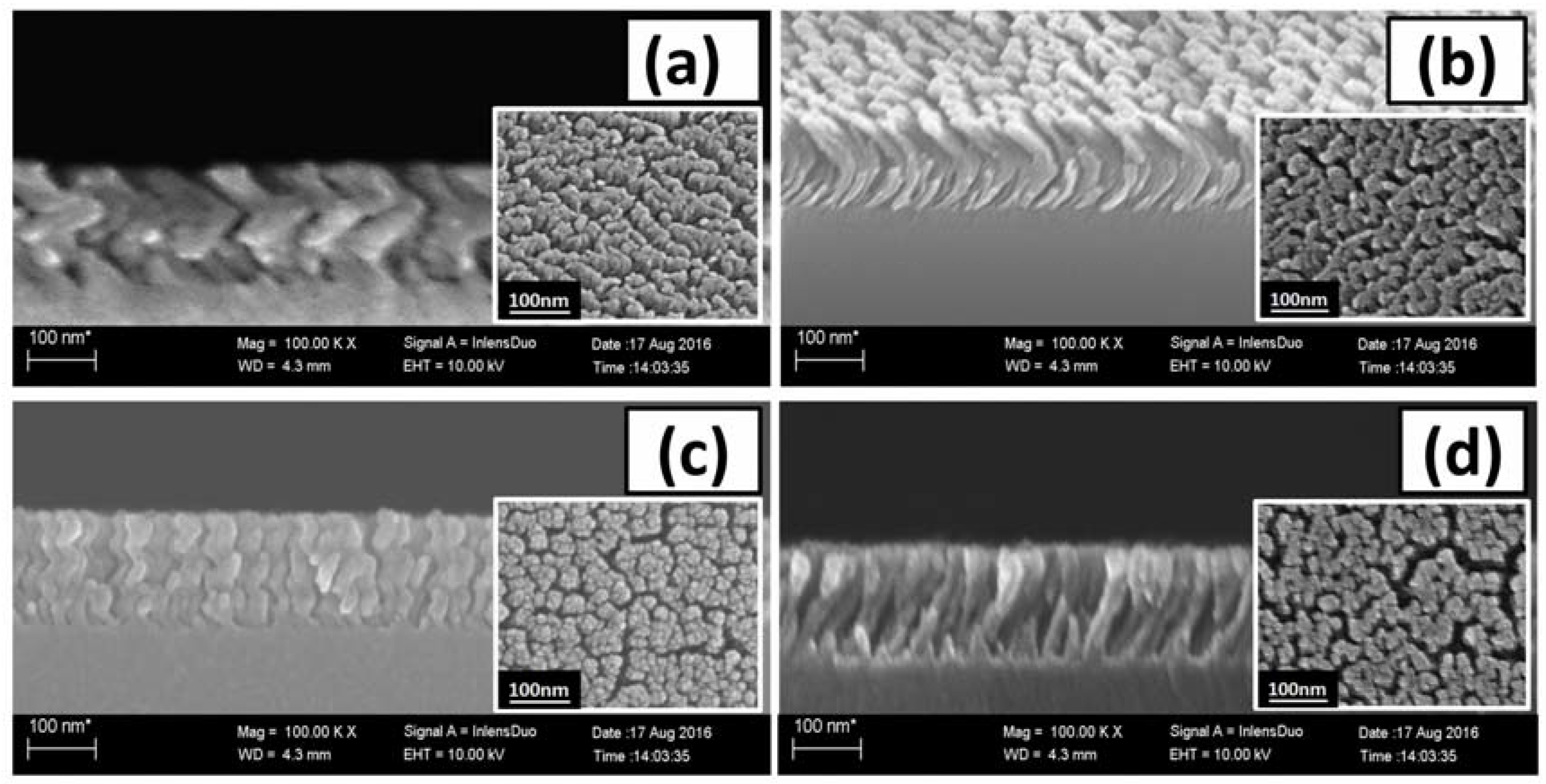
According to experimental requirements, the growing nanostructures morphology can be modified easily by monitoring the substrate rotational condition, stationary position, deposition angle, or the vapour flux arrival during the fabrication process. We also fabricate different morphologies of SiO2 nanostructures such as nanozigzag, nanohelix, slanting and C-shape SiO2 nanofilms by controlling and adjusting the substrate position as shown in Figure 1. Figure 1a represents the SiO2 nanozigzag film. The zigzag nanostructure can be easily established by instigating the vapour flux arrival direction to rotate the substrate holder by 180° repeatedly in clockwise and anticlockwise directions while the deposition angle was kept constant at 80° throughout the deposition process. Similarly, C-Shape nanofilms and nanohelics can be fabricated by rotating substrates at a constant rate comparative to the deposition rate. Thus, a columnar C-shape (0.06 Rev/min) or nanohelics (0.12 Rev/min) formation takes place comprised of constant pitches depending on the rotational speed of the substrate with respect to revolution per time.
Slanting nanorods as shown in Figure 1d is fabricated by a slanting substrate holder with respect to the target normal direction by an angle of 80° keeping the substrate holder stationary, and thickness of the developing film is controlled by a deposition rate measured via QCM. The QCM determines variation in mass flux per unit area by computing the frequency change. When target materials having high melting points are deposited at room temperature under high vacuum in a tilt substrate position, then the vapour flux arrives at a normal substrate, which results in growing columnar nanostructures. SEM images observably indicate that deposition angle plays a key role in monitoring the nanostructure morphology of thin films due to limited atom mobility and self-shadowing effect. Cross-sectional SEM images show that, in all the fabricated SiO2 nanostructures, the inter-column spaces increase, due to which extremely oriented, nanocolumn development proceeds. The nanocolumns in spite of any shape show good separation, consistency, uniformity and homogeneity with periodical void spaces between growing nanostructures as shown in Figure 1.
3.2. Refractive Index Analysis
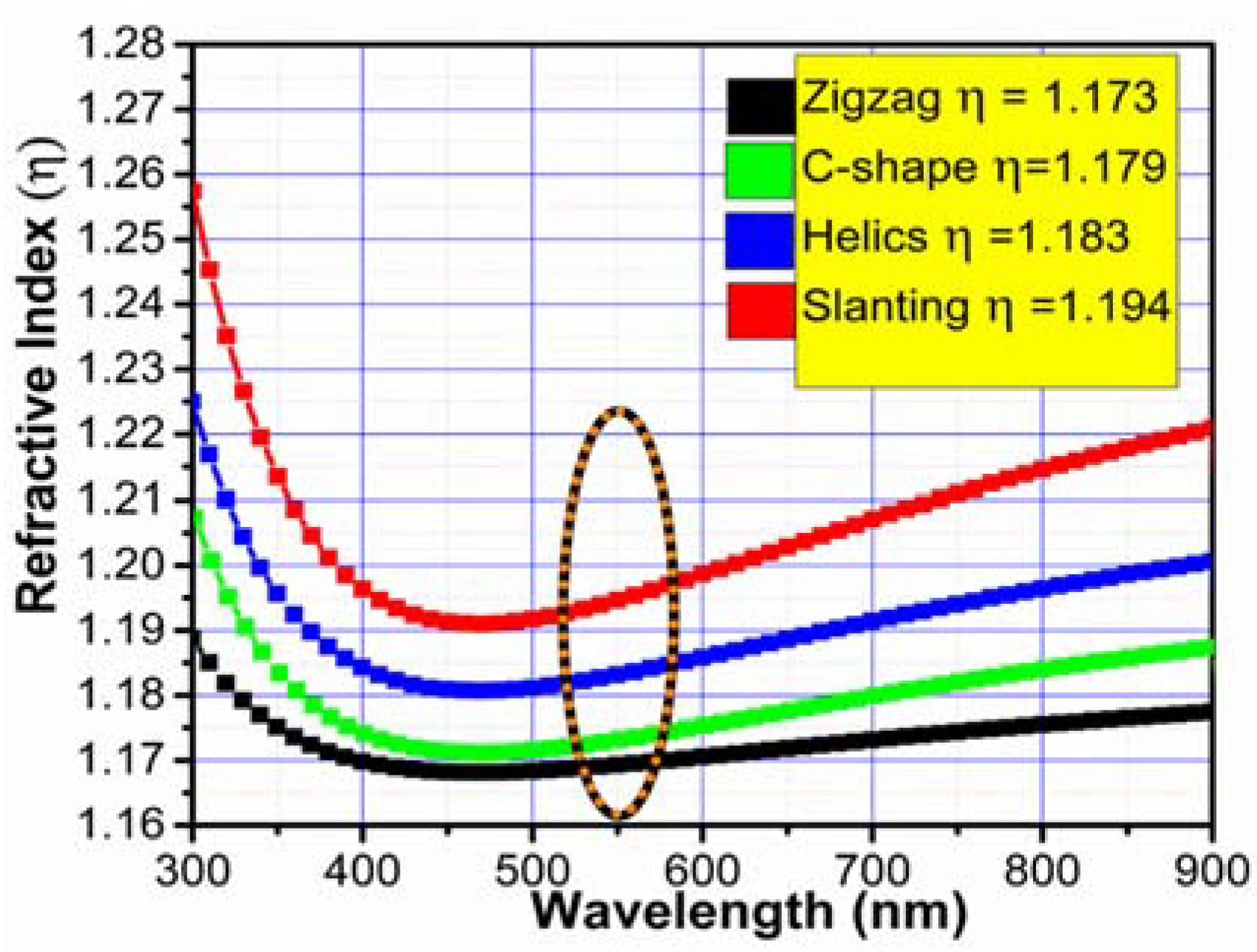
The refractive index of SiO2 nanostructures was determined by using a WVASE32 spectroscopic ellipsometer (JA Woollam Co., Inc., Lincoln, NE, USA) in the wavelength range of 300–900 nm. The η of SiO2 nanostructures were calculated by using the Cauchy dispersion model, as SiO2 is transparent and dielectric. The experimental results show that there is a slight variation in the refractive index of thin films at 550 nm wavelength, as shown in Figure 2.
The nanozigzag and C-shape SiO2 nanostructures nearly show the same η = 1.17. However, SiO2 nanohelix structures show the η = 1.18. Earlier in our previous experiments, we deposited standing nanorods that almost show the same refractive index of 1.18 [24]. Slanting SiO2 nanorods show the highest refractive index of 1.19 among all fabricated nanostructures at a deposition angle of 80°. The experimental results prove that overall there is a very slight influence on the refractive index of thin films by changing the morphology of nanostructures keeping the deposition angle the same. The η value remains in between 1.17–1.19 at angle 80° by changing morphology. In thin films, the main cause for the decrement in the effective refractive index is due to an upsurge in porosity, which influences the packing density and mass fraction. Figure 2 indicates that nanozigzag SiO2 film shows higher porosity in comparison with other nanostructures. Overall, all of the SiO2 nanofilms are very permeable, spongy and porous comprised of mass flux and void air spaces.
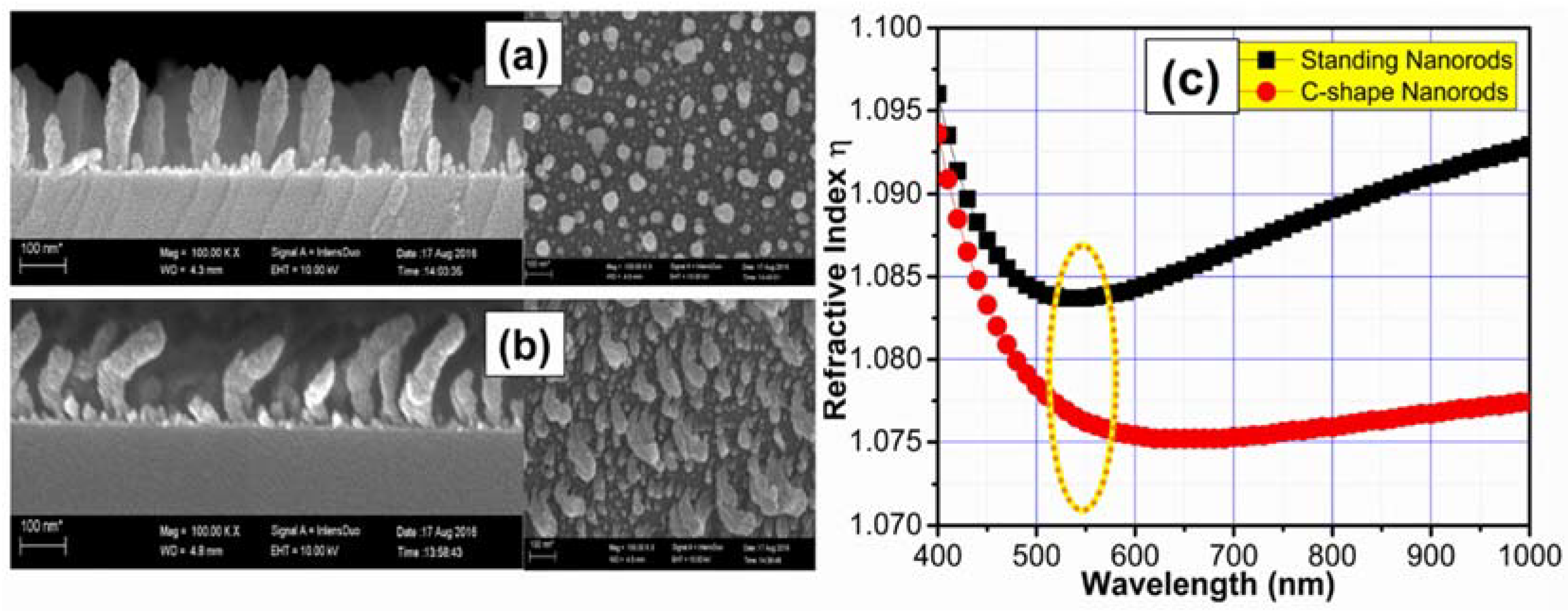
In order to prove and validate our findings of the nanostructure influence on the refractive index, we use the maximum glancing angle 88° and fabricate nanostructures with varying morphologies including standing [24], and C-shape nanofilms as shown in Figure 3. The experimental results show that, at such high oblique angle, there are minor differences in refractive index still existing at the nanolevel. The SEM top and cross-sectional images clearly indicate that nanofilms are highly oriented, well-spaced, homogenous, and separated. Figure 3a,b shows the standing nanorods, and C-shape nanofilms fabricated at a glancing angle of 88° with fast substrate rotational and slow rotation. Figure 3c shows the refractive index of SiO2 standing, and C-shape measured as a function of wavelength at 550 nm. The refractive index analysis shows that there is a very slight negligible influence of refractive index at a glancing angle of 88°. Overall morphology did not impact the refractive index at 88° and it lies in between 1.07–1.08.
3.3. Fabrication of SiO2 AR Coatings
In fabricating AR coatings, optical thickness and η play an important role in reducing the reflectance of the desired substrate. In our experiments, we deposit bilayer SiO2 AR coatings comprised of a dense layer and a porous layer on top of the dense layer to reduce the reflectance of BK7 glass substrate less than 1 percent in the visible region. Firstly, the dense film is deposited on the forward-facing side at deposition angle 0° having a refractive index of 1.46 at 550 nm wavelength [34]. On the top of the dense film, a porous vertical nanostructure having lower η than the bottom layer was deposited at an oblique angle (α) of 80°.
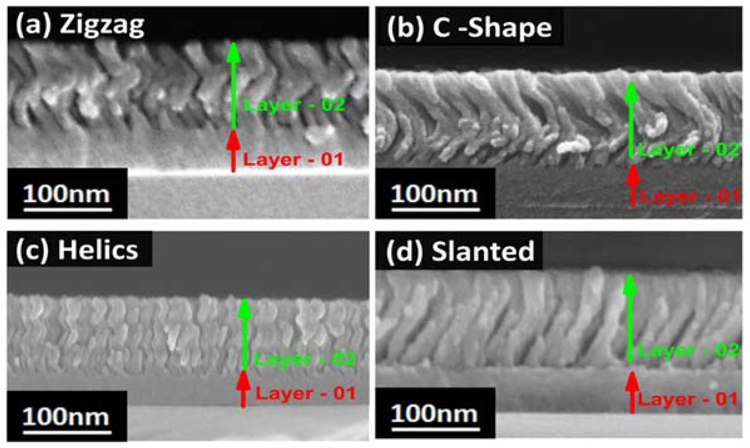
Both layers were deposited in a single step just by changing the tilting position of the substrate to avoid any foreign contamination or dust influence. The oblique angle was preferred to induce porosity as well as to generate a steady deviation in η of AR coating stack from surrounding air towards the substrate bottom. Figure 4 clearly represents the cross-sectional SEM image of bilayer SiO2 AR coatings having different morphologies on BK7 substrate. The SEM image clearly shows the interfaces between the dense layer and the top porous layer having different morphologies comprised of nanozigzag, C-shape, nanohelix, and slanting nanostructure. In all cases, the bottom layer is deposited at angle 0° and the top layer is deposited at angle 80°. The edges of two layers in the SiO2 AR stack and the supporting substrate is clearly evident, indicating the consistency and regularity within the individual layer throughout the thickness of nanostructure representing stability and consistency in the refractive index profile.
3.4. AR Efficiency of SiO2 AR Coatings
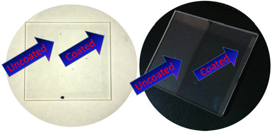
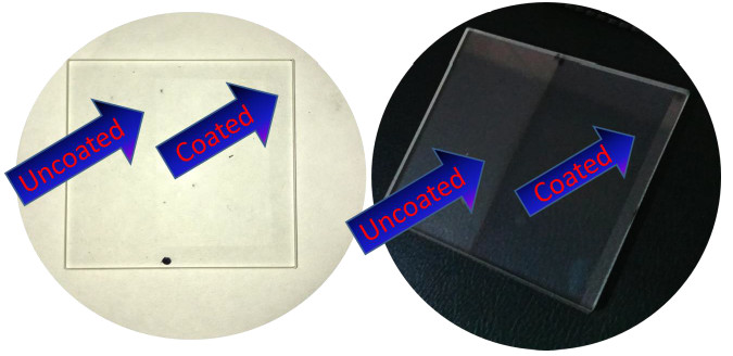
The angle-resolved microscope (ARM) R1 series Ideaoptics is used to determine the reflectance properties of bilayer SiO2 AR coatings at the normal light incidence and omnidirectional angles. BK7 substrate reflects 4.26%–5% in the wavelength range between 500–900 nm. Fabricating bilayer SiO2 AR coating reduces the reflectance of BK7 to <1% reflectance in the wavelength range 500–900 nm as shown in Figure 5. The measured experimental reflectance (dE) outcomes of fabricated bilayer SiO2 AR coating are quite analogous to each other displaying <1% reflectance as shown in Figure 5 in the visible region.
The fabrication parameters i.e., the deposition angle and individual layer thickness in bilayer SiO2 AR coating stack is mentioned in Table 1. The experimental result shows that AR efficiency of nanozigzag is better than the other SiO2 AR coatings having different morphologies. Nanozigzag bilayer SiO2 AR coating shows less <1% reflectance in the whole visible region 470–850 nm at normal incidence angle. C-shape and nanohelix bilayer SiO2 AR coatings show nearly identical AR efficiency (<1%) in the wavelength range of 520–900 nm. Slanting SiO2 AR coatings shows a slight decrement in efficiency (540–850 nm) in comparison with other SiO2 AR coatings. The reason is due to a slight variation in refractive index of top layers in comparison with other coatings throughout the wavelength range (300–900 nm).
Here, the bilayer SiO2 AR films were fabricated according to simulation parameters. The simulated AR curves are similar to experimental reflectance curves of as-deposited SiO2 AR films, as shown in Figure 5a–d. The thickness of each individual layer in bilayer coating stack information is taken by simulated design AR film as mentioned in Table 1. The experimental fabricated thickness of bilayer SiO2 AR films is identical to the thickness of the individual layer of a simulated design AR coating stack. The simulated thickness is represented by dS and experimentally fabricated AR film thickness is abbreviated as dE, as stated in Table 1. The experimental results show that, by optimizing the thickness of the individual layer in a coating stack and selecting the appropriate refractive index, one can design AR coatings according to optical instrument requirements at the desired wavelength region.
3.5. Omnidirectional AR Efficiency of SiO2 AR Coatings
Practically in different optoelectronic appliances, AR coating encompassing wideband reflectance over a wide light incident angles (AOI) is mandatory and prerequisite. Here, we also determine the AR efficiency of our fabricated coatings at a different angle of light incidence via full angle reflection (FAR) operational mode. The omnidirectional AR capacity of bilayer SiO2 AR coating having different morphologies is shown in Figure 6.
The experimental measurement demonstrates that, in the visible wavelength range, bilayer SiO2 AR coating having zigzag morphology preserves its AR proficiency uniformly at oblique angles. The zigzag SiO2 AR coating reflecting 0.01%–0.58% light in the wavelength range of 530–850 nm at oblique angles varies from normal incidence 90° up to 50° with 5° change. Similarly, the bilayer SiO2 AR coating having different morphologies Figure 6b C-shape, Figure 6c nanohelix and Figure 6d slanting nanostructure also show omnidirectional AR efficiency at a different angle of light incidence. In C-shape SiO2 AR coatings, the films show <1% reflectance in the entire visible spectra. In the wavelength range of 650–750 nm, C-shape SiO2 AR coatings show <0.29% light, while, at 550–650 nm and 750–850 nm, it shows <0.58% showing good omnidirectional characteristics.
A similar kind of omnidirectional efficiency is observed in helical SiO2 AR coatings displaying <0.48% light in the wavelength range of 550–850 nm wavelength. Thus, the experimental result shows that fabricated AR coating is omnidirectional. In case of slanting SiO2 AR coatings (Figure 6d), the coating shows <0.5% reflectance in the wavelength range between 550–700 nm at different angles of light incidence. However, at oblique angles of 60° and 55°, the AR efficiency declines towards higher wavelength regions (650–750 nm) showing nearly 1%–2% reflectance. Beyond this wavelength (i.e., 750–850 nm), the AR film reflects nearly 2%–3% light. Overall, the performance of AR coatings having different morphologies is stable and consistent in visible spectra showing an incident-angle-insensitive antireflective omnidirectional characteristic.
3.6. Negative Temperature Stability
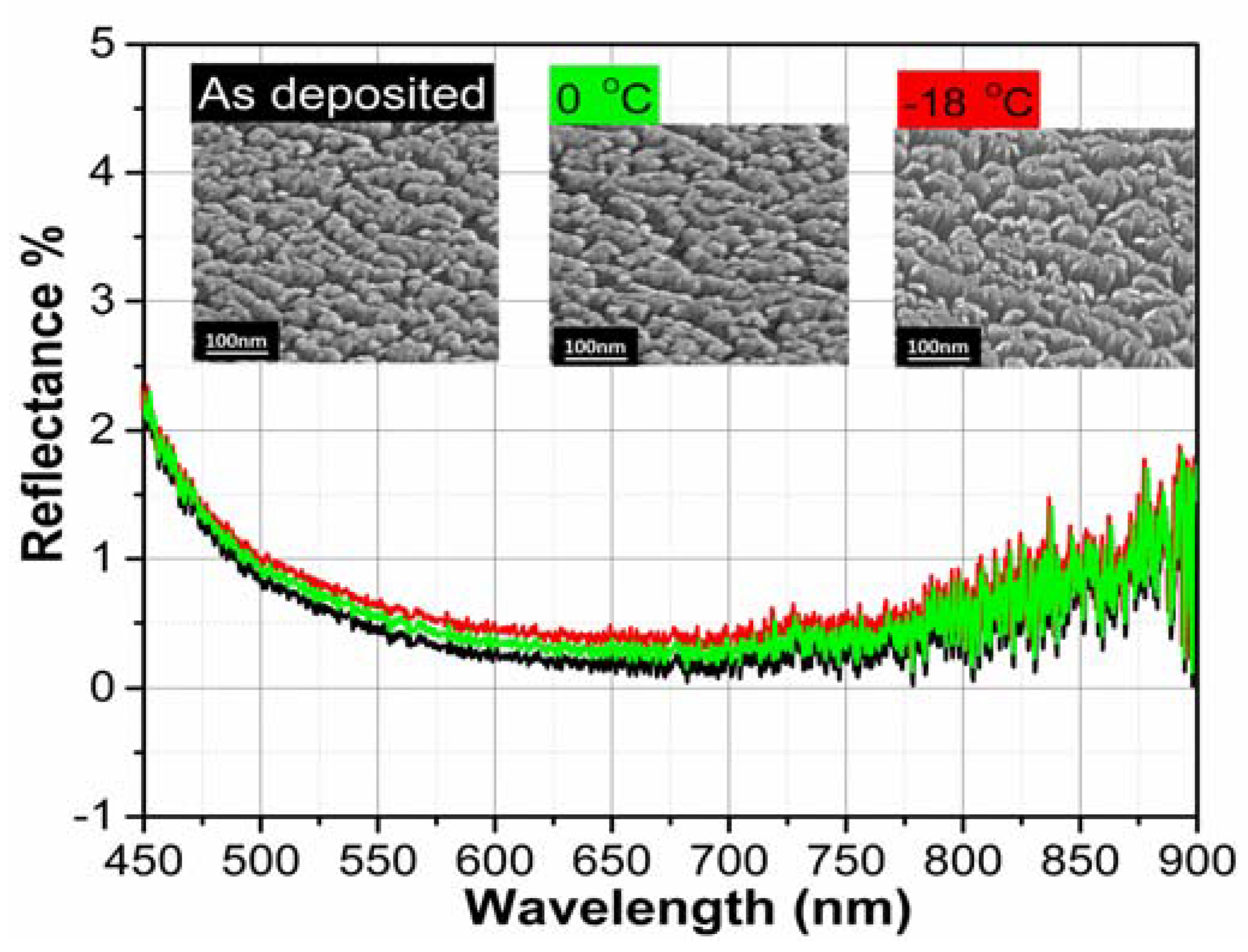
Experiments were also carried at a negative temperature to investigate the AR efficiency of nanozigzag bilayer SiO2 coating. We keep the bilayer SiO2 AR films at 32 °F (0 °C, refrigerator) and 0 °F (−18 °C) for 24 h in order to study the negative temperature impact on the AR efficiency of as-deposited bilayer SiO2 coating. The experimental result displays that the AR film retains its AR efficiency even when exposed to such low temperatures. The as-deposited and negative exposed nanozigzag bilayer SiO2 coating shows similar AR efficiency when measured at normal incidence angle. There is a very negligible variation in AR efficiency (towards lower wavelength region 500 nm) of as-deposited SiO2 AR coating and cold storage SiO2 AR coating after exposure to 24 h at 0 °C, and −18 °C, as shown in Figure 7. The inset in Figure 7 shows SEM images of as-deposited and cold storage nanozigzag bilayer SiO2 AR coatings, showing that there is no change in morphology taking place. Due to this, there is consistency and no worsening occurs in AR performance of bilayer SiO2 thin films.
3.7. Annealing Influence on AR Proficiency of SiO2 AR Coatings
Annealing experiments were also performed to examine the AR proficiency of nanozigzag bilayer SiO2 coating at a higher temperature. The SiO2 AR coating was annealed for an hour at 100, 200, 300 and 350 °C with a ramp speed of 5 °C, as shown in Figure 8. At 100 °C, the as-deposited SiO2 AR coating and annealed SiO2 AR coating show nearly identical AR efficiency as there is no influence of annealing. At 200 °C and 300 °C, there is negligible slight declination in AR efficiency in comparison with as-deposited AR coating. However, the SiO2 AR coating shows <1% reflectance in the visible region retaining its AR performance. After annealing at 350 °C, a clear shift of reflectance minima is observed in comparison with as deposit AR coating. The AR efficacy of SiO2 AR coating at 350 °C deteriorates due to structural defects, lattice stresses, increased packing density or crystallization [34]. Overall, the SiO2 AR films are thermally stable up to 300 °C without any deterioration in AR efficiency. Beyond this temperature (350 °C), there is a slight increment in AR efficiency due to induced crystallinity, which influences packing density of thin films in the declining of the AR efficacy [34].
3.8. Contact Angle Measurement
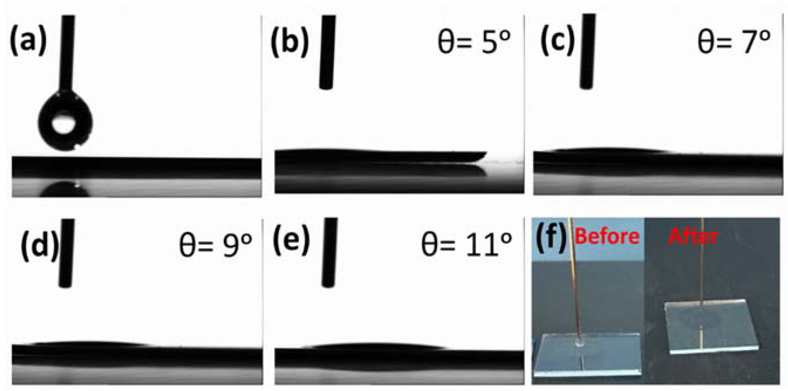
The wetting behaviour of coatings is a significant phenomenon for its practical usage in real-world applications i.e., TiO2 self-cleaning coatings for photocatalysis [37,38,39,40]. The contact angle (CA) parameter is used to describe the hydrophobicity or hydrophilicity of a surface. In our experiments, the sessile drop method is used to determine the static contact angle of SiO2 AR coatings having different nanostructures. The experimental result demonstrates that our fabricated AR coatings are super hydrophilic in nature, showing a water contact angle θ < 12° as shown in Figure 9.
The CA measurements show that SiO2 AR coatings having nanozigzag and C-shape morphology show super hydrophilic behaviour with a CA of nearly 5° and 7°. Nanohelix and slanting nanostructure also show the same kind of hydrophilic behaviour as shown in Figure 9d,e. The CA measurements were performed at five different locations on AR coatings and the average result is reported here for accuracy. Figure 9f clearly demonstrates the spreading of water droplets after it drops on SiO2 AR coating. Hydrophilicity and wettability performance of SiO2 AR coatings depend on nanostructure, chemical composition and surface geometrical dimension. The hydrophilicity characteristic in our fabricated SiO2 AR coating generates a self-cleaning ability in AR films as the water spreads instantaneously over the surface, rather enduring as droplets. The hydrophilic behaviour in thin films improves the removal of the dirt particles and makes the surface dry quicker. Thus, SiO2 AR coating offers an intriguing route in different optics applications because of it self-cleaning ability, thermal stability and omnidirectional AR performance.
4. Conclusions
A PVD method for the fabrication of SiO2 thin films that transforms refractive index from 1.45 to 1.07 has been established by changing the deposition angle. The omnidirectional optical behaviour of SiO2 AR coating could be easily varied by the rational design of film structure and the choice of the substrate material. It was experimentally proved that the AR film exhibits a significant decrement in reflectance in comparison with the uncoated supporting substrate. The outstanding performance of experimentally fabricated coating could be attributed to the design parameters of a bilayer coating on a transparent substrate. The current coating design advantage is that it is reliable, easy to fabricate, consistent and appropriate for different substrates (transparent or semitransparent). One can easily reduce the reflectance of the desired substrate only by regulating the discrete stratum thinness and selecting the appropriate refractive index in a coating stack. One of the noteworthy characteristics of the design is the absence of property incongruity influence at the interface and least contamination impact since the two distinct layers comprise a single structure. Our experimental result proves that the morphology slightly impacts the refractive index of nanostructures when deposited at the same angle at the nanolevel. The fabricated bilayer SiO2 AR coatings having different morphologies demonstrate self-cleaning ability, thermal stability and omnidirectional AR efficiency as well as AR constancy when exposed to negative temperature. Engineering graded-index morphologies at the nanolevel is an effective methodology to engender identical properties such as lotus like superhydrophobicity or being reminiscent of moth eyes. These kinds of AR coatings are a good choice in optoelectronic devices operational in negative temperature environments.
Author Contributions
Z.Z. and H.W. conceived and designed the experiments; S.B.K. performed the experiments; analyzed the data and wrote the paper; Z.Z. also financed the providing of materials, analysis tools and equipment.
Funding
This research was supported by the Basic Science Center Project of NSFC (Grant No. 51788104), the National Natural Science Foundation of China (Grant No. 51572148 and No. 51531006), and the Tsinghua University Initiative Scientific Research Program.
Conflicts of Interest
The authors declare no conflict of interest. The funding sponsors had no role in the design of the study; in the collection, analyses, or interpretation of data; in the writing of the manuscript, and in the decision to publish the results.
References
- Sun, J.; Zhang, C.; Zhang, C.; Ding, R.; Xu, Y. Effect of post-treatment on ordered mesoporous silica antireflective coating. RSC Adv. 2014, 4, 50873–50881. [Google Scholar] [CrossRef]
- Zou, L.; Li, X.; Shen, J. Preparation and properties of ordered mesoporous silica antireflective coating with high strength. Rare Met. Mater. Eng. 2016, 45, 472–476. [Google Scholar]
- Xu, L.; He, J. Antifogging and antireflection coatings fabricated by integrating solid and mesoporous silica nanoparticles without any post-treatments. ACS Appl. Mater. Interfaces 2012, 4, 3293–3299. [Google Scholar] [CrossRef] [PubMed]
- Carlstrom, J.E.; Ade, P.A.R.; Aird, K.A.; Benson, B.A.; Bleem, L.E.; Busetti, S.; Chang, C.L.; Chauvin, E.; Cho, H.M.; Crawford, T.M. The 10 meter south pole telescope. Publ. Astron. Soc. Pac. 2009, 123, 568–581. [Google Scholar] [CrossRef]
- Kelzenberg, M.D.; Boettcher, S.W.; Petykiewicz, J.A.; Turnerevans, D.B.; Putnam, M.C.; Warren, E.L.; Spurgeon, J.M.; Briggs, R.M.; Lewis, N.S.; Atwater, H.A. Enhanced absorption and carrier collection in Si wire arrays for photovoltaic applications. Nat. Mater. 2010, 9, 239–244. [Google Scholar] [CrossRef] [PubMed]
- Zou, M.; Thompson, C.; Fleming, R.A. Antireflective Coating for Glass Applications and Method of Forming Same. U.S. Patent WO2014134594A1, 4 September 2014. [Google Scholar]
- Moghal, J.; Kobler, J.; Sauer, J.; Best, J.; Gardener, M.; Watt, A.A.R.; Wakefield, G. High-performance, single-layer antireflective optical coatings comprising mesoporous silica nanoparticles. ACS Appl. Mater. Interfaces 2011, 4, 854–859. [Google Scholar] [CrossRef] [PubMed]
- Xu, L.; He, J. A novel precursor-derived one-step growth approach to fabrication of highly antireflective, mechanically robust and self-healing nanoporous silica thin films. J. Mater. Chem. C 2013, 1, 4655–4662. [Google Scholar] [CrossRef]
- Lu, Y.; Zhang, X.; Huang, J.; Li, J.; Wei, T.; Lan, P.; Yang, Y.; Xu, H.; Song, W. Investigation on antireflection coatings for Al:ZnO in silicon thin-film solar cells. Opt. Int. J. Light Electron. Opt. 2013, 124, 3392–3395. [Google Scholar] [CrossRef]
- Wu, F.; Dantan, J.Y.; Etienne, A.; Siadat, A.; Martin, P. Improved algorithm for tolerance allocation based on Monte Carlo simulation and discrete optimization. Comput. Ind. Eng. 2009, 56, 1402–1413. [Google Scholar] [CrossRef]
- Menezes, E.H.S.D.C.; König, P.; Jilavi, M.H.; Oliveira, P.W.D.; Júnior, S.A. Carboxylic acids and esters as scaffold for cavities in porous single layer anti-reflective coatings of silica-titania with excellent optical and mechanical properties. Mater. Sci. Appl. 2014, 5, 783–788. [Google Scholar] [CrossRef]
- Li, T.; He, J. Mechanically robust, humidity-resistant, thermally stable high performance antireflective thin films with reinforcing silicon phosphate centers. Sol. Energy Mater. Sol. Cells 2017, 170, 95–101. [Google Scholar] [CrossRef]
- Khristyan, V.A.; Zagoruiko, Y.A.; Kovalenko, N.O.; Mateychenko, P.V.; Sofronov, D.S. Thermally stable antireflection coatings for active elements of ZnMgSe:Cr2+–laser: Preparation and properties. Funct. Mater. 2011, 18, 462–465. [Google Scholar]
- Doroshenko, M.E.; Osiko, V.V.; Jelínková, H.; Jelínek, M.; Šulc, J.; Němec, M.; Vyhlídal, D.; Čech, M.; Kovalenko, N.O.; Gerasimenko, A.S. Spectroscopic and laser properties of bulk iron doped zinc magnesium selenide Fe:ZnMgSe generating at 4.5–5.1 µm. Opt. Express 2016, 24, 19824–19834. [Google Scholar] [CrossRef] [PubMed]
- Abdul Hadi, S.; Milakovich, T.; Bulsara, M.T.; Saylan, S. Design optimization of single-layer antireflective coating for GaAs1−xPx/Si Tandem Cells With x = 0, 0.17, 0.29, and 0.37. IEEE J. Photovolt. 2014, 5, 425–431. [Google Scholar] [CrossRef]
- Saylan, S.; Milakovich, T.; Hadi, S.A.; Nayfeh, A.; Fitzgerald, E.A.; Dahlem, M.S. Multilayer antireflection coating design for GaAs 0.69 P 0.31/Si dual-junction solar cells. Sol. Energy 2015, 122, 76–86. [Google Scholar] [CrossRef]
- Bernal-Correa, R.; Morales-Acevedo, A.; Mora, A.; Pulzara, L.; Monsalve, J.M. Design of AlxGa1−xAs/GaAs/InyGa1−yAs triple junction solar cells with anti-reflective coating. Mater. Sci. Semicond. Process. 2015, 37, 57–61. [Google Scholar] [CrossRef]
- Khan, S.B.; Wu, H.; Huai, X.; Zou, S.; Liu, Y.; Zhang, Z. Mechanically robust antireflective coatings. Nano Res. 2018, 11, 1699–1713. [Google Scholar] [CrossRef]
- Kim, S.; Cho, J.; Char, K. Thermally stable antireflective coatings based on nanoporous organosilicate thin films. Langmuir 2007, 23, 6737–6743. [Google Scholar] [CrossRef] [PubMed]
- Wang, S.; Yan, H.; Li, D.; Qiao, L.; Han, S.; Yuan, X.; Liu, W.; Xiang, X.; Zu, X. TEM and STEM studies on the cross-sectional morphologies of Dual-/Tri-layer broadband SiO2 antireflective films. Nanoscale Res. Lett. 2018, 13, 49. [Google Scholar] [CrossRef] [PubMed]
- Huang, X.; Yuan, Y.; Liu, S.; Wang, W.; Hong, R. One-step sol-gel preparation of hydrophobic antireflective SiO2 coating on poly(methyl methacrylate) substrate. Mater. Lett. 2017, 208, 62–64. [Google Scholar] [CrossRef]
- Kennedy, S.R.; Brett, M.J. Porous broadband antireflection coating by glancing angle deposition. Appl. Opt. 2003, 42, 4573–4579. [Google Scholar] [CrossRef] [PubMed]
- Li, J.; Lu, Y.; Lan, P.; Zhang, X.; Xu, W.; Tan, R.; Song, W.; Choy, K.L. Design, preparation, and durability of TiO2/SiO2 and ZrO2/SiO2 double-layer antireflective coatings in crystalline silicon solar modules. Sol. Energy 2013, 89, 134–142. [Google Scholar] [CrossRef]
- Zhao, J.; Green, M.A. Optimized antireflection coatings for high-efficiency silicon solar cells. IEEE Trans. Electron Devices 1991, 38, 1925–1934. [Google Scholar] [CrossRef]
- Zhang, J.; Lan, P.; Li, J.; Xu, H.; Wang, Q.; Zhang, X.; Zheng, L.; Lu, Y.; Dai, N.; Song, W. Sol-gel derived near-UV and visible antireflection coatings from hybridized hollow silica nanospheres. J. Sol-Gel Sci. Technol. 2014, 71, 267–275. [Google Scholar] [CrossRef]
- Du, X.; He, J. Facile fabrication of hollow mesoporous silica nanospheres for superhydrophilic and visible/near-IR antireflection coatings. Chem. Eur. J. 2011, 17, 8165–8174. [Google Scholar] [CrossRef] [PubMed]
- Zhang, L.; Du, K.; Zhou, L.; Tu, H. Preparation of silica antireflective coating for UV-laser. Acta Opt. Sin. 1996, 16, 998–1001. [Google Scholar]
- Belleville, P.F.; Floch, H.G. Ammonia hardening of porous silica antireflective coatings. In Proc. SPIE 2288, Sol-Gel Optics III, Proceedings of SPIE’s 1994 International Symposium on Optics, Imaging, and Instrumentation, San Diego, CA, USA, 24-29 July 1994; Mackenzie, J.D., Ed.; SPIE: Bellingham, WA, USA, 1994. [Google Scholar] [CrossRef]
- Wang, K.; He, J. One-Pot fabrication of antireflective/antibacterial dual-function Ag NP-containing mesoporous silica thin films. ACS Appl. Mater. Interfaces 2018, 13, 11189–11196. [Google Scholar] [CrossRef] [PubMed]
- Mazur, M.; Wojcieszak, D.; Domaradzki, J.; Kaczmarek, D.; Song, S.; Placido, F. TiO2/SiO2 multilayer as an antireflective and protective coating deposited by microwave assisted magnetron sputtering. Opto-Electron. Rev. 2013, 21, 233–238. [Google Scholar] [CrossRef]
- Wuu, D.S.; Lin, C.C.; Chen, C.N.; Lee, H.H.; Huang, J.J. Properties of double-layer Al2O3/TiO2 antireflection coatings by liquid phase deposition. Thin Solid Films 2015, 584, 248–252. [Google Scholar] [CrossRef]
- Huang, J.J.; Lee, Y.T. Self-cleaning and antireflection properties of titanium oxide film by liquid phase deposition. Surf. Coat. Technol. 2013, 231, 257–260. [Google Scholar] [CrossRef]
- Kuo, C.F.J.; Tu, H.M.; Su, T.L. Optimization of the electron-beam-lithography parameters for the moth-eye effects of an antireflection matrix structure. J. Appl. Polym. Sci. 2006, 102, 5303–5313. [Google Scholar] [CrossRef]
- Khan, S.B.; Wu, H.; Li, J.; Chen, L.; Zhang, Z. Bilayer SiO2 nanorod arrays as omnidirectional and thermally stable antireflective coating. Adv. Eng. Mater. 2018, 20, 1700942. [Google Scholar] [CrossRef]
- Vicente, G.S.; Bayón, R.; Germán, N.; Morales, A. Long-term durability of sol–gel porous coatings for solar glass covers. Thin Solid Films 2009, 517, 3157–3160. [Google Scholar] [CrossRef]
- Khan, S.B.; Wu, H.; Ma, L.; Hou, M.; Zhang, Z. HfO2 nanorod array as high-performance and high-temperature antireflective coating. Adv. Mater. Interfaces 2017, 4, 1600892. [Google Scholar] [CrossRef]
- Shirolkar, M.; Kazemian Abyaneh, M.; Singh, A.; Tomer, A.; Choudhary, R.; Sathe, V.; Phase, D.; Kulkarni, S. Rapidly switched wettability of titania films deposited by dc magnetron sputtering. J. Phys. D Appl. Phys. 2008, 41, 1525–1528. [Google Scholar] [CrossRef]
- Takeda, S.; Suzuki, S.; Odaka, H.; Hosono, H. Photocatalytic TiO2 thin film deposited onto glass by DC magnetron sputtering. Thin Solid Films 2001, 392, 338–344. [Google Scholar] [CrossRef]
- Pérez-González, M.; Tomás, S.A.; Santoyo-Salazar, J.; Morales-Luna, M. Enhanced photocatalytic activity of TiO2–ZnO thin films deposited by dc reactive magnetron sputtering. Ceram. Int. 2017, 12, 8831–8838. [Google Scholar] [CrossRef]
- Pérez-González, M.; Tomás, S.A.; Morales-Luna, M.; Arvizu, M.A.; Tellez-Cruz, M.M. Optical, structural, and morphological properties of photocatalytic TiO2–ZnO thin films synthesized by the sol–gel process. Thin Solid Films 2015, 594, 304–309. [Google Scholar] [CrossRef]
Figure 1.
Cross-sectional images of SiO2 nanostructures: (a) nanozigzag, (b) C-Shape, (c) nanohelix, and (d) slanting nanorods. The inset in each figure represents the top view morphology of thin films.
Figure 1.
Cross-sectional images of SiO2 nanostructures: (a) nanozigzag, (b) C-Shape, (c) nanohelix, and (d) slanting nanorods. The inset in each figure represents the top view morphology of thin films.

Figure 2.
Refractive index (η) of SiO2 nanozigzag, nanohelix, slanting and C-shape nanofilms measured as a function of wavelength at 550 nm.
Figure 2.
Refractive index (η) of SiO2 nanozigzag, nanohelix, slanting and C-shape nanofilms measured as a function of wavelength at 550 nm.

Figure 3.
Shows the (a) standing nanorods (reproduced with permission from [34]; © 2018 WILEY-VCH Verlag GmbH & Co. KGaA), and (b) C-shape nanofilms fabricated at glancing angle of 88°; (c) the refractive index of SiO2 standing and C-shape nanofilm calculated as a function of wavelength at 550 nm.
Figure 3.
Shows the (a) standing nanorods (reproduced with permission from [34]; © 2018 WILEY-VCH Verlag GmbH & Co. KGaA), and (b) C-shape nanofilms fabricated at glancing angle of 88°; (c) the refractive index of SiO2 standing and C-shape nanofilm calculated as a function of wavelength at 550 nm.

Figure 4.
Bilayer SiO2 AR coatings having different morphologies on BK7 substrate: (a) nanozigzag, (b) C-shape, (c) nanohelix, and (d) slanting nanostructure.
Figure 4.
Bilayer SiO2 AR coatings having different morphologies on BK7 substrate: (a) nanozigzag, (b) C-shape, (c) nanohelix, and (d) slanting nanostructure.

Figure 5.
Bilayer SiO2 AR coating efficiency on BK7 substrate: (a) nanozigzag, (b) C-shape, (c) nanohelix, and (d) slanting nanostructures. Blue curves represent the simulated reflectance of design coating. The black curve represents reflectance from the uncoated substrate. Coloured curves represent the experimentally measured reflectance results of fabricated bilayer SiO2 AR coatings.
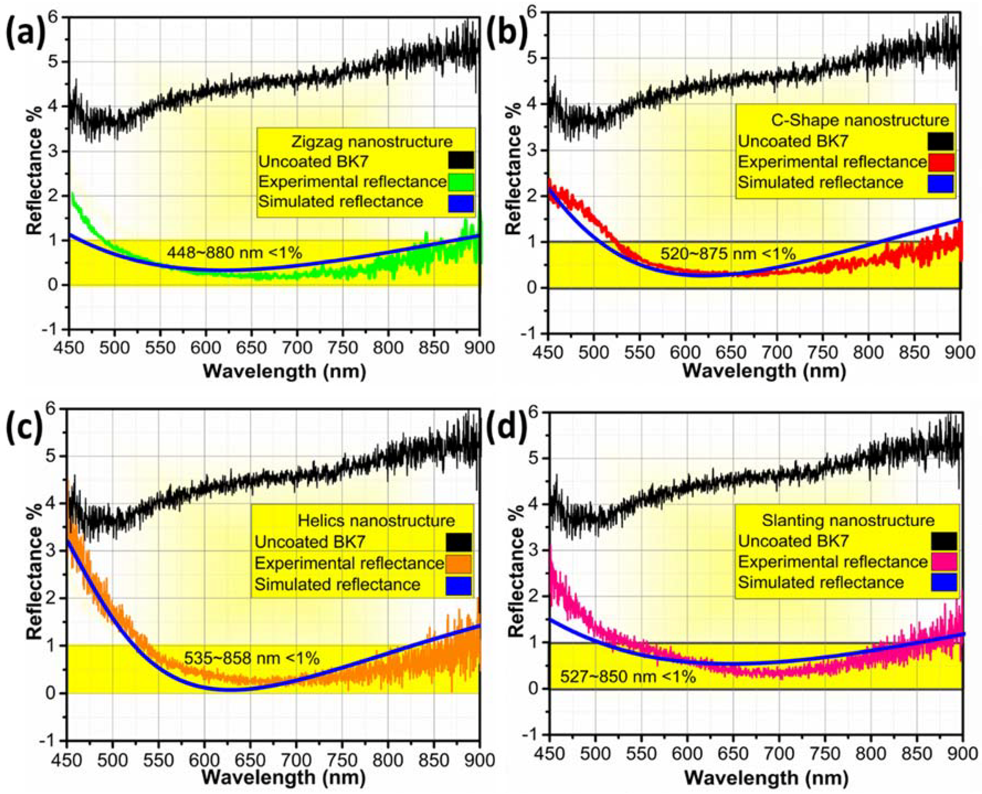
Figure 6.
Omnidirectional AR efficiency of bilayer SiO2 AR coating on BK7 substrate at a different angle of light incidence: (a) nanozigzag, (b) C-shape, (c) nanohelix, and (d) slanting nanostructure.
Figure 6.
Omnidirectional AR efficiency of bilayer SiO2 AR coating on BK7 substrate at a different angle of light incidence: (a) nanozigzag, (b) C-shape, (c) nanohelix, and (d) slanting nanostructure.

Figure 7.
Experimentally calculated AR efficiency of as-deposited nanozigzag SiO2 AR coating and cold storage SiO2 coating at 0 °C, and −18 °C, The inset represents the top morphology of as-deposited AR and negative temperature exposed SiO2 AR coating.
Figure 7.
Experimentally calculated AR efficiency of as-deposited nanozigzag SiO2 AR coating and cold storage SiO2 coating at 0 °C, and −18 °C, The inset represents the top morphology of as-deposited AR and negative temperature exposed SiO2 AR coating.

Figure 8.
AR efficiency of as-deposited and annealed nanozigzag SiO2 AR coating at 100, 200, 300 and 350 °C.
Figure 8.
AR efficiency of as-deposited and annealed nanozigzag SiO2 AR coating at 100, 200, 300 and 350 °C.
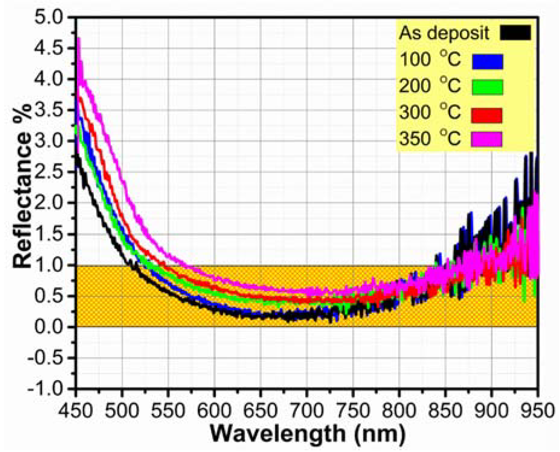
Figure 9.
Contact angle measurement of SiO2 AR coating on BK7 substrate (a) showing droplet volume of 5 µL use to measure contact angle, (b) nanozigzag, (c) C-shape, (d) nanohelix, (e) slanting nanostructure, and (f) represents the droplet spreading behavior before and after droplet removal from needle.


Table 1.
Bilayer SiO2 AR coating fabrication parameters.
| Morphology | Deposition Angle (α) | Refractive Index (η) | Thickness (nm) dS | Thickness (nm) dE | ||||
|---|---|---|---|---|---|---|---|---|
| Layer-1 | Layer-2 | Layer-1 | Layer-2 | Layer-1 | Layer-2 | Layer-1 | Layer-2 | |
| Nanozigzag | 0 | 80 | 1.45 | 1.173 | 65 | 130 | 70 | 130 |
| C-shape | 0 | 80 | 1.45 | 1.179 | 75 | 135 | 78 | 141 |
| Nanohelix | 0 | 80 | 1.45 | 1.18 | 60 | 142 | 56 | 147 |
| Slanting | 0 | 80 | 1.45 | 1.19 | 64 | 130 | 56 | 125 |
© 2018 by the authors. Licensee MDPI, Basel, Switzerland. This article is an open access article distributed under the terms and conditions of the Creative Commons Attribution (CC BY) license (http://creativecommons.org/licenses/by/4.0/).
Share and Cite
MDPI and ACS Style
Khan, S.B.; Wu, H.; Zhang, Z. Omnidirectional SiO2 AR Coatings. Coatings 2018, 8, 210. https://doi.org/10.3390/coatings8060210
AMA Style
Khan SB, Wu H, Zhang Z. Omnidirectional SiO2 AR Coatings. Coatings. 2018; 8(6):210. https://doi.org/10.3390/coatings8060210
Chicago/Turabian StyleKhan, Sadaf Bashir, Hui Wu, and Zhengjun Zhang. 2018. "Omnidirectional SiO2 AR Coatings" Coatings 8, no. 6: 210. https://doi.org/10.3390/coatings8060210
Note that from the first issue of 2016, this journal uses article numbers instead of page numbers. See further details here.