Morphological Characteristics of Au Films Deposited on Ti: A Combined SEM-AFM Study


Dipartimento di Fisica e Astronomia, Università di Catania and MATIS CNR-IMM, via S. Sofia 64, 95123 Catania, Italy
*
Author to whom correspondence should be addressed.
Coatings 2018, 8(4), 121; https://doi.org/10.3390/coatings8040121
Submission received: 3 March 2018
/
Revised: 16 March 2018
/
Accepted: 24 March 2018
/
Published: 26 March 2018
(This article belongs to the Special Issue Thin Films for Advance Applications)
Abstract
:Deposited Au films and coatings are, nowadays, routinely used as active or passive elements in several innovative electronic, optoelectronic, sensing, and energy devices. In these devices, the physical properties of the Au films are strongly determined by the films nanoscale structure. In addition, in these devices, often, a layer of Ti is employed to promote adhesion and, so, influencing the nanoscale structure of the deposited Au film. In this work, we present experimental analysis on the nanoscale cross-section and surface morphology of Au films deposited on Ti. In particular, we sputter-deposited thick (>100 nm thickness) Au films on Ti foils and we used Scanning Electron Microscopy to analyze the films cross-sectional and surface morphology as a function of the Au film thickness and deposition angle. In addition, we analyzed the Au films surface morphology by Atomic Force Microscopy which allowed quantifying the films surface roughness versus the film thickness and deposition angle. The results establish a relation between the Au films cross-sectional and surface morphologies and surface roughness to the film thickness and deposition angle. These results allow setting a general working framework to obtain Au films on Ti with specific morphological and topographic properties for desired applications in which the Ti adhesion layer is needed for Au.
1. Introduction
Deposited Au films and coatings are, nowadays, routinely used as active or passive elements in several innovative electronic, optoelectronic, sensing, and energy devices [1,2,3]. These technologies require exploitation of the electronic, magnetic, optical, mechanical and thermal properties unique to metallic materials. Generally, the prerequisites for a “good” metallization include strong adhesion, high electrical conductivity, and a clean interface with the contacting material [4,5]. The problems connected to these aspects are well-known from the development of the microelectronics era [4,5], where metal films and coatings were used on semiconductors or oxides as electrical contacts and interconnections [6]. Metallic coatings have known a renewed interest with the development of the nanotechnology era [1,2,3]. In fact, deposited metallic films, having nanoscale thickness, present artificial physical properties enhancing the performances of several devices [1,2,3]. In this sense, for example, they find application in the production of solar cell devices, complementary metal-oxide-semiconductor (CMOS) devices, sensing devices, etc. by exploiting their structure-dependent electronic, magnetic, optical, and thermal properties [1,2,3]. As specific examples: (a) the continuing downscaling of CMOS devices poses stringent requirements on the optimization and reliability of all components of the devices [3]. With the approaching of the quantum electronic devices with a projection of a gate length of 4–5 nm [3] it is likely that metal contacts will play a crucial role. It can be anticipated, however, that the successful downscaling demand high-performance contacting metals in terms film thickness, crystallographic phase, and surface/interface morphology; (b) the mechanical properties of metallic films often determine the reliability of electronic, optical, magnetic devices [3]. During operation of devices employing metallic coatings, very significant stresses, can develop in the metallic films (especially for very thin films) causing distortion and even failure. Therefore, the strict control of the metal film structure (in terms of structural and chemical defects) is essential in establish the final device reliability so as in the next-generation micro- and nano-electro-mechanical-systems (MEMS and NEMS) [3]; magnetic thin films having nanoscale controlled structure present unique properties such as magnetocrystalline, interfacial and shape anisotropy [3]. The characteristic of these anisotropies can be finely controlled by the control of the film nanoscale morphology and employed in magnetic recording devices, sensing devices, etc. [3]; metal films have been shown to guide light in visible, infrared, and terahertz portions of the electromagnetic spectrum by coupling radiation to surface plasmons [3]. However, characteristics such as plasmons mode propagation length and coupling efficiency, depends upon the optical properties of metallic films which are, in turn, determined by the structural ones [3].
In this general context, the wide-range control and modification of the metal film nano-morphology is crucial in the exploitation of their properties for desired applications, and this can be as result of the control of the deposition process parameters [7]. One of the prime concerns towards the reliability of these technologies is the adhesion strength of the metal film to the semiconductor or insulator substrate (which can be quantified, for example, by the adhesion energy Eadh = γfv + γsv − γfs (J/m2), being γfv the metal film surface energy, γsv the semiconductor or insulator substrate surface energy, and γfs the film-substrate interface energy) [1,2,3,6,8,9,10,11]. Therefore, adhesion is a characteristic property of the film-substrate system on the basis of the material forming the two system components, involving the materials atomic bonding. In addition, in real systems, adhesion is dependent on the mechanical properties of the two materials brought into contact. In particular, the mechanical properties of thin films of materials (i.e., fracture and deformation properties) are, often, very different from those of the corresponding bulk materials making the adhesion behavior of the film-substrate system different from that of the corresponding bulk-bulk materials system [6]. Gold is widely used as metallic coating for semiconductors and oxides due to the wide range of properties it offers on the nanoscale, ranging from the optical ones (i.e., plasmonic, in particular) to the electrical ones [1,2,3]. However, since Au does not easily bond well to semiconductors and oxides (SiO2 is the main example), a layer of titanium or titanium oxide is employed to promote adhesion [8,9,10,11,12]. In most cases, the Au metallization of semiconductors and oxides surfaces requires a high adhesive strength of the Au layer to increase the mechanical reliability of the micro- and nano-electronics devices [1,2,3,4,5,6,12,13,14,15]. In this regard, prior to the formation of an Au electrode layer on the semiconductor or oxide substrates, Ti or TiO2 are usually deposited to strongly bind the substrate and Au together. Au, as other metals, poorly wet semiconductors and oxides and cluster in three-dimensional particles when deposited on these substrates. For example, the adhesion energy of these metals to SiO2 is, typically, between 0.2 and 1.0 J/m2. However, the insertion of Ti or TiO2 buffer layers between metals and SiO2 increases the adhesion energy by more than one order of magnitude [10]. On the other hand, the insertion of the Ti or TiO2 adhesion layer greatly affects the nanoscale morphology of the Au film which is grown on it. The final nano-morphology of the deposited film is determined by the competing kinetic and thermodynamic processes occurring for the adatoms on a surface (diffusion, nucleation, etc.) [7]. These processes are largely influenced by the interaction of the deposited atoms with the atoms of the substrate (since this interaction affects the adatoms surface diffusion). In this regard, in particular, the nanoscale control of the Au film structure is crucial towards the determination of its properties in view of applications in functional nano-devices. For example, the roughness of deposited metal films is one of the most critical determining final electrical, optical and other properties of the systems [16,17,18,19,20,21,22,23,24,25]. As examples: (a) one of the key issue in the modern integrated circuit technology is the dramatic increase in metallic interconnect resistivity with decreasing cross section thickness. This effect, by increasing the time delay, seriously affects the future evolution of the microelectronic devices [18]. Below 100 nm thickness, the electrons scattering process by the metal film surface roughness becomes more and more pronounced and becoming predominantly below 50 nm thickness. In this sense, the fabrication of ultraflat metallic films (with roughness much smaller than the electrons mean free path) is essential is essential in limiting the surface roughness scattering process; (b) the surface plasmonic properties of rough metal films can be exploited for the fabrication of ultra-sensitive Raman-based sensing devices [19]. In these devices, the nanoscale film roughness strongly affects the surface enhancement factor of the Raman spectroscopy. The surface roughness dictates, in fact, both the metal surface exposed area and the overall interaction of the light with the metal on the nanoscale level; (c) the surface roughness of metal films establishes, on the nanoscale level, the characteristics of the light interaction with the film. As a consequence, the roughness determines the absorbing and scattering properties of the metal film. By controlling these properties, thin metal films are exploited as light absorbing or scattering elements in plasmonic solar cells or other optical devices [20,21,22,23]; (d) laser-induced photochemistry on metal surfaces is widely studied as an effective means to catalyze surface reactions for specific adsorbates [24]. However, the surface roughness of the metal film was proved to greatly impacts on the rate of the reactions by controlling the light absorption in the metal film; (e) surface roughness dictates, also, the surfaces wetting properties and its nanoscale control is essential for designing and controlling wetting processes in general. This is particularly important in the extreme case of ultra-hydrophobic surfaces, for which roughness results in very high water contact angles and very low water roll-off angles [25].
Therefore, it is clear the recent importance devoted by the scientific research on nanoscale rough metal surface and in the development of methods to produce, on surfaces, metal films with controlled and desired surface roughness.
On the basis of the previous considerations, the aim of the present paper is to report on the experimental analysis of the nanoscale cross-section and surface morphology of thick Au films (>100 nm thickness, in contrast to ultrathin Au films with thickness <10 nm and thin Au films with thickness in the 10–100 nm range) deposited on Ti. The results of these analyses, performed by Scanning Electron Microscopy (SEM) and Atomic Force Microscopy (AFM), allow to set a general working framework to obtain Au films on Ti with specific morphological and topographic properties for desired applications in which the Ti adhesion layer is needed for Au.
2. Materials and Methods
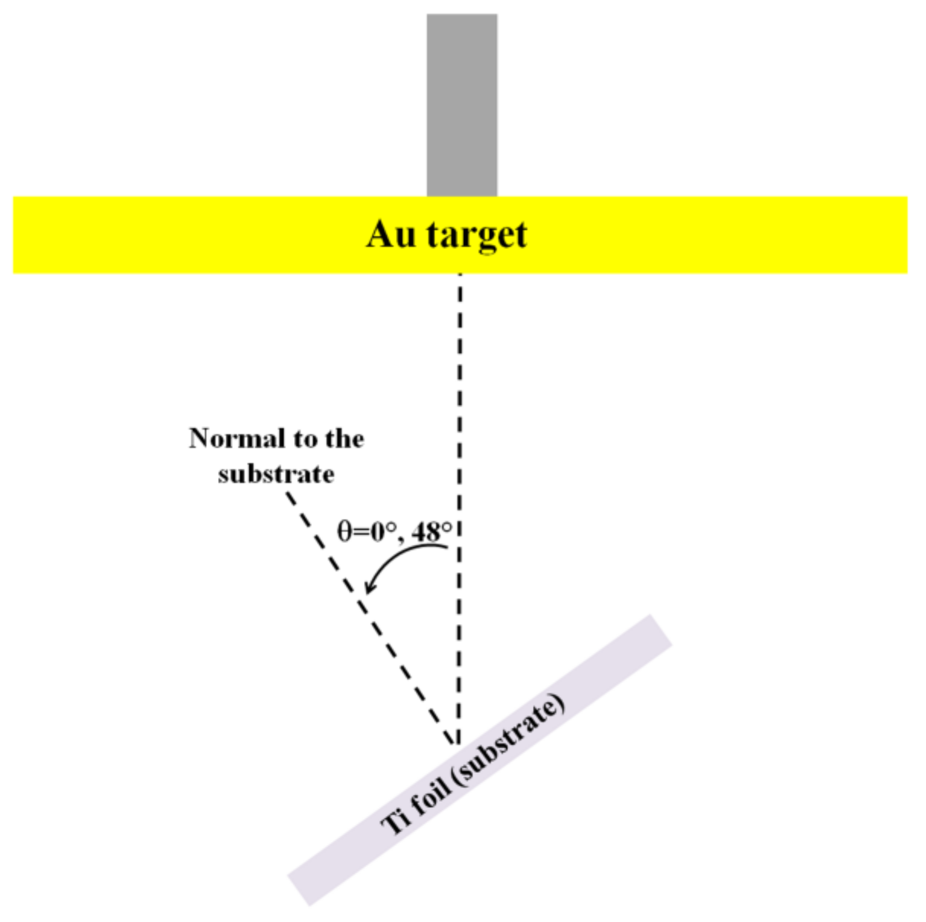
99.99%-pure Ti foil (with a few angstroms thick layer of titania on the surface) was purchased from Sigma-Aldrich (St. Louis, MO, United States) [26]. Slides (about 1 cm × 1 cm) were cut from the starting Ti foil. Regarding the Au depositions on the Ti slides, Au foil (99.999% purity, 6 cm diameter) was used as sputtering target. The Au sputtering depositions on the Ti slides were performed by using a RF Emitech K550X sputter coater (Laughton, East Sussex, UK) employing Ar gas for the sputtering process at a pressure of 0.02 mbar during the depositions. The depositions were carried out maintaining the Ti substrates at room temperature ad stationary and at a distance of 40 mm from the Au target. During the Au depositions, the working current was fixed to 50 mA while the deposition time was fixed to 20 or 32 min, so to change the resulting Au film thickness on the Ti substrate. In addition, the Au depositions were performed in normal incidence (maintaining the substrate parallel to the target, θ = 0°) or in oblique incident (fixing an angle of θ = 48° between the normal direction to the substrate and the normal direction to the target), see the scheme in Figure 1. The Au film growth rate r depends on the substrate inclination [27,28,29,30,31,32]: in normal incidence condition, Au films of thickness h0 ~ 220 nm (20 min deposition, namely sample A1), or 350 nm (32 min deposition, namely sample A2) are obtained (r0 ~ 0.18 nm/s), while in oblique incidence condition, Au films of thickness h48 ~ 140 nm (20 min deposition, namely sample B1), or 230 nm (32 min deposition, namely sample B2), corresponding to h0 cos(48°) [27,28,29,30,31,32], are obtained (r48 ~ 0.12 nm/s). Table 1 summarizes the fabricated samples.
A Zeiss FEG-SEM Supra 25 Microscope (Oberkochen, Germany) was employed to perform the cross-sectional and plan view Scanning Electron Microscopy (SEM) analyses of the deposited Au films (using an acceleration voltage of 5 kV). Also AFM analyses of the deposited Au film surfaces were performed by using a Bruker-Innova microscope (Billerica, MA, USA) operating in high-amplitude mode. Concerning these analysis, ultra-sharpened Si tips were used (MSNL-10 from Bruker Instruments, Billerica, MA, United States, with anisotropic geometry, radius of curvature ~2 nm, tip height ~2.5 μm, front angle ~15°, back angle ~25°, side angle 22.5°, nominal spring constant of 0.07 N/m). The Si tips were substituted as soon as a resolution loose was observed during the AFM images acquisition. The AFM images were analyzed by using the SPMLABANALYSES V7.00 software to extract values for the RMS (Root Mean Square) of the Au films surface.
3. Results and Discussions
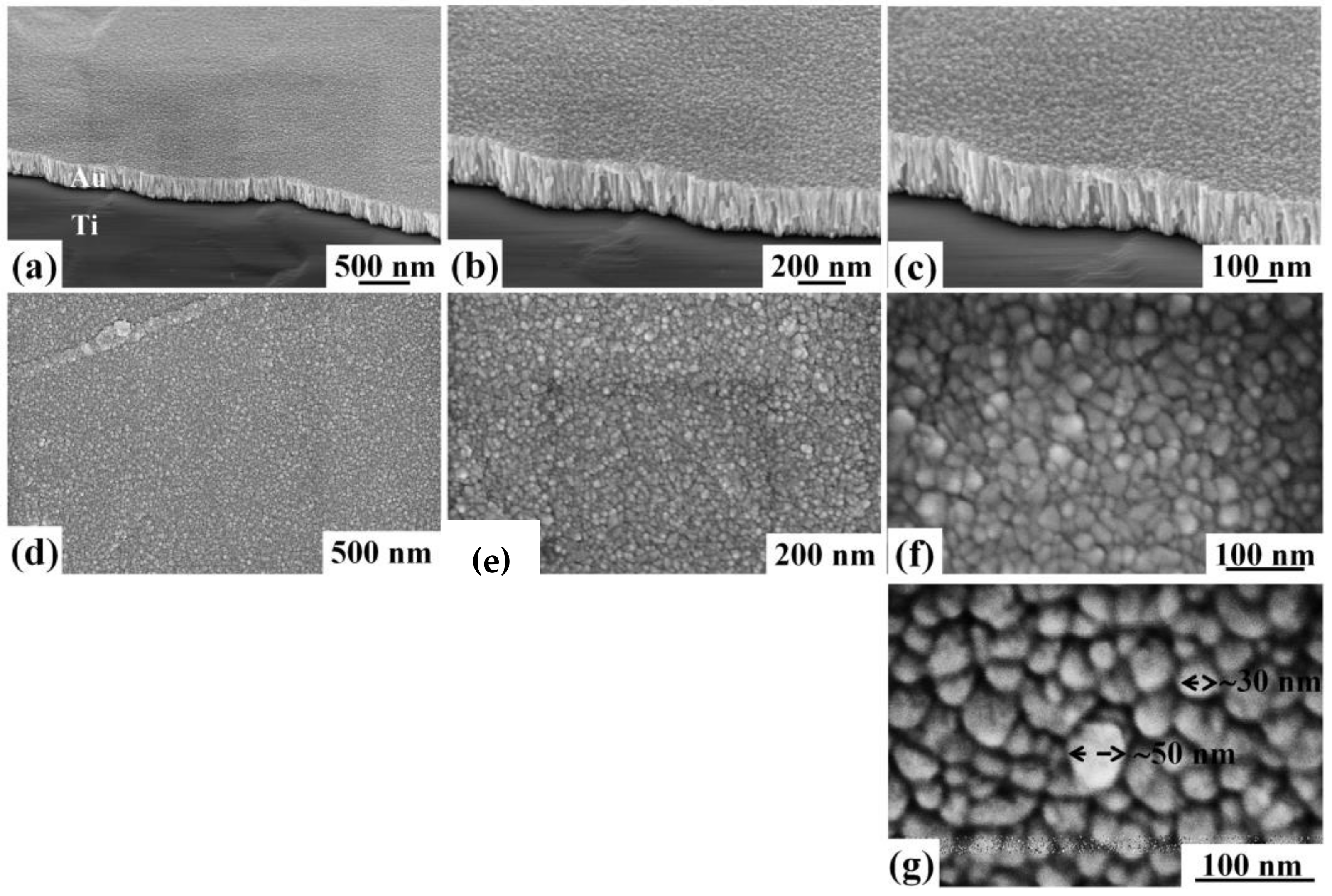
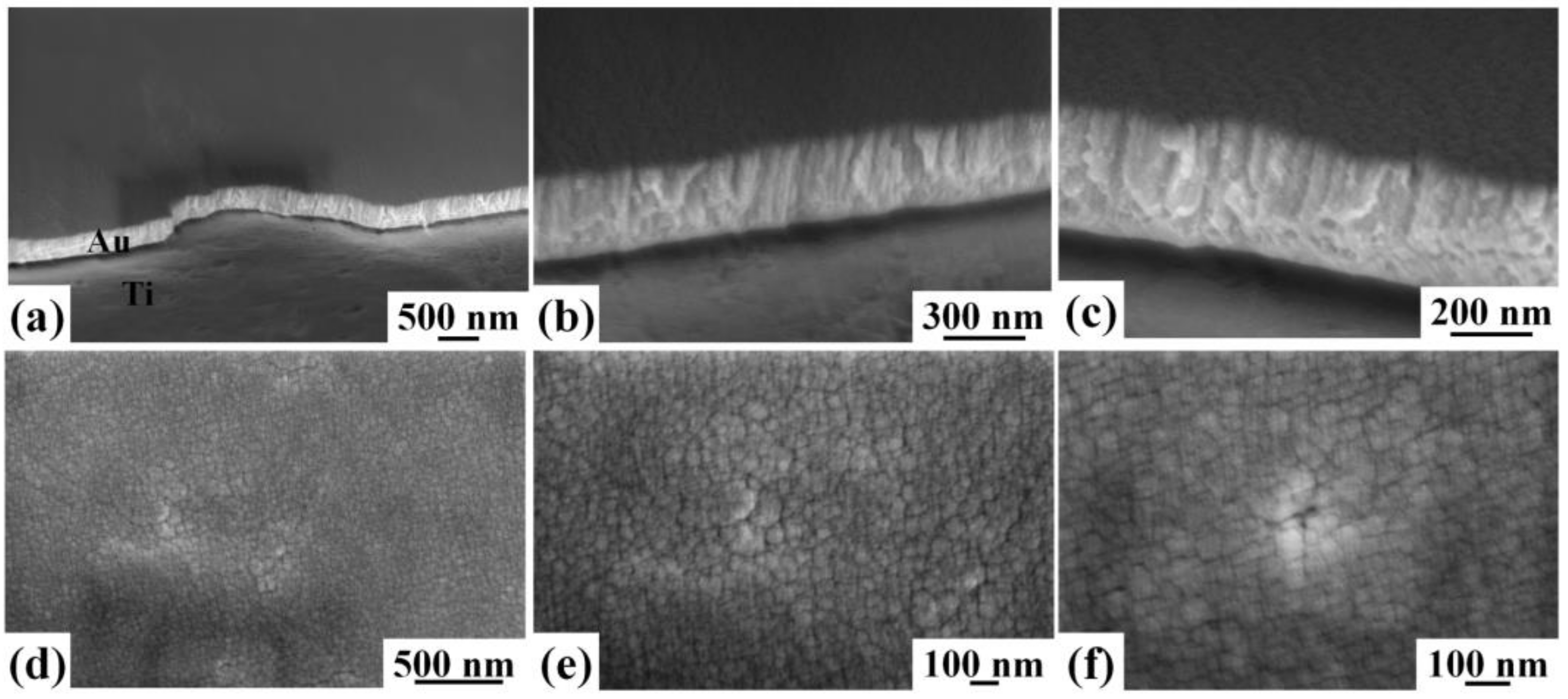
First of all, we report cross-sectional and plan-view SEM micrographs of the Au films deposited on Ti in the various conditions. Figure 2 reports the SEM micrographs for sample A1 (θ = 0°, 20 min deposition, h0 ~ 220 nm), cross-views with increasing magnification from Figure 2a–c, and plan-views with increasing magnification from Figure 2d–g. Figure 3 presents the SEM micrographs for sample A2 (θ = 0°, 32 min deposition, h0 ~ 350 nm), cross-views with increasing magnification from Figure 3a–c, and plan-views with increasing magnification from Figure 3d–f. Then, Figure 4 reports the SEM micrographs for sample B1 (θ = 48°, 20 min deposition, h48 ~ 140 nm), cross-views with increasing magnification from Figure 4a–c, and plan-views with increasing magnification from Figure 4d–f. Finally, Figure 5 shows the SEM micrographs for sample B2 (θ = 48°, 32 min deposition, h0 ~ 230 nm), cross-views with increasing magnification from Figure 5a–c, and plan-views with increasing magnification from Figure 5d–f.
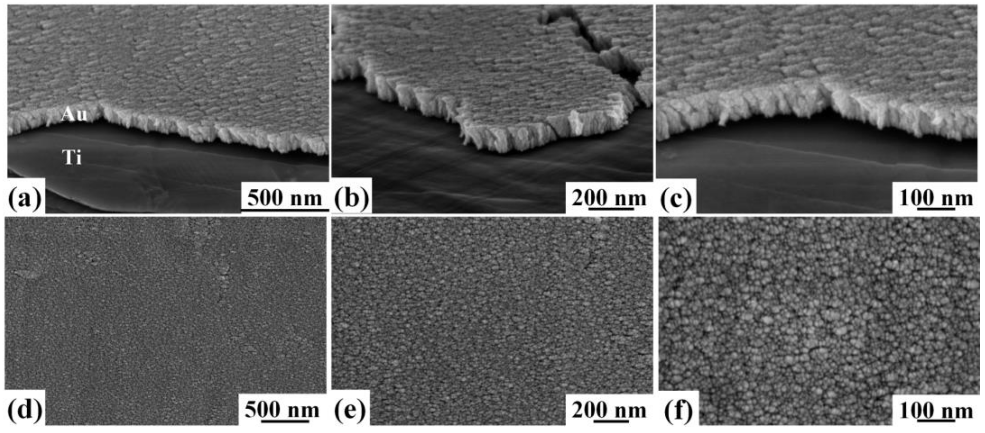
In particular, observing the images in Figure 2, it is evident that in sample A1 (θ = 0°, 20 min deposition, h0 ~ 220 nm) the Au film on Ti is a uniform and dense layer. It can be recognized, in this case, that the film is formed by dense touching grains which are elongated perpendicularly to the substrate. The plan dimensions of these elongated grains ranges, roughly, from about 20 nm to about 60 nm (see Figure 2g characterized by the highest magnification). However, even if compact, the film clearly shows a columnar structure. This columnar structure establishes the peculiar surface morphology (Figure 2d–f) in which round-shaped structures (each corresponding to the top-side of a column) are evident.
Concerning, instead, the thicker Au film (350 nm, 32 min deposition) deposited in normal incidence condition, as imaged in Figure 3, the columnar structure is yet recognizable but it is less evident from the cross-sectional images ((a)–(c)) leading, also, to a more flat surface morphology with respect to the thinner Au film. In discussing these first results, we observe that the Au adatoms, upon arriving over the substrate surface from the atomic vapor generated from the source (Au target), perform a random walk (i.e., surface diffusion) on the surface which can be quantitatively described by the surface diffusion coefficient D = D0exp[−EA/kT] (D and D0 measured in m2/s, and EA J (or eV) so as kT), being D0 (the pre-exponential factor) related to the adatom attempt frequency from a surface site to another, EA the activation energy for the hopping phenomenon, k the Boltzmann constant and T the absolute temperature at which the adatoms hopping process occurs [31,33]. Key factors establishing EA are, for example, the interatomic energy between the adatoms and the substrate atoms and between the adatoms themselves. The very first step of the Au film growth is the Au clusters formation (homogeneous and/or heterogeneous nucleation stage). The characteristics of such a stage are of paramount importance in establishing the structural properties (defects, stress, etc.) of the final grown film after the overall deposition process. In this nucleation stage, the surface density of the adatoms is very low, so that atomic interaction is, mainly, between the adatoms and the substrate atoms. However, in this stage, the surface deposited adatoms interact, also, with the new atoms continuously arriving from the vapor-phase during the deposition. Therefore, this interaction becomes a competitive phenomenon to the adatoms surface diffusion process: the final film morphology will be determined, eventually, by the competition between the adatoms surface diffusion and the rate of arriving atoms from the vapor-phase. As an extreme case, at very high deposition rates, adatoms on the substrate surface are buried under newly impinging atoms, limiting, so, the adatoms joining rate to other diffusing adatoms but becoming potential nucleation site for the arriving atoms from the vapor-phase. In the opposite case, at very low deposition rates, the adatoms can probe a very high surface area per unit time, leading to a high nucleation rate at surface defects and high joining rate for diffusing adatoms. It is evident that, continuing the deposition, these two extreme situations will lead films with different nanoscale structure and morphology. We can summarize the above observations by considering, as final result, that the adatoms surface diffusion length LD = (t the diffusion time) is, also, established by the deposition rate [27,31]. The overall parameters determining the adatoms mobility on the substrate surface can be summarized as the adatom-surface interaction, the substrate temperature, the atoms deposition rate from the vapor-phase, and the energy of the atoms arriving on the surface from the vapor-phase. All these kinetics and thermodynamics parameters concur in establishing the film growth characteristics and, so, the final film nanoscale morphology. We focus, now, our attention, in particular, on the effect of the adatom-surface interaction on the adatoms mobility. A general rough classification distinguishes atoms which are chemisorbed or physioadsorbed on the substrate surface [27]. Chemisorbed atoms chemically react with the surface atoms establishing strong chemical bindings with typical binding energies of the 1 eV order. Physioadsorbed atoms, instead, interact weakly with the surface atoms, mainly by van der Waals forces. In this case, the binding energy is, typically, in the 0.3–0.4 eV range. Obviously, this distinction greatly impacts on the adatoms surface mobility: higher the binding energy between adatoms and surface atoms lower, then, the adatoms surface mobility. Fixed the chemical nature of atoms to be deposited (in addition to the substrate temperature, atoms arriving rate from the vapor-phase, and energy of the arriving atoms), the substrate can be changed to pass from chemisorbed adatoms to physioadsorbed adatoms. Chemisorbed adatoms will be characterized by a lower diffusion length with respect to physioadsorbed adatoms. This classification leads to conclude, roughly, that chemisorbed adatoms on the surface could be potential nucleation sites for newly arriving atoms, while physioadsorbed adatoms tend to condensate at surface preferential sites (defects or impurities). It is clear that in these two extreme cases, continuing the deposition, films of the same material will be formed but with very different nanoscale structure and morphology and, as a consequence, with very different properties such as density, adhesion behaviour, etc. In the specific case of Au films, these considerations justify why Ti or TiO2 layers are usually used as adhesion layers for Au films on oxides (SiO2, for example). In fact, the binding energy of Au atoms to Ti atoms is quite large (Nagata et al. [9], in particular, quantified the improvement of the adhesive strength of Au on Ti with respect to SiO2). Therefore, in the discussion of the nano-morphology of the Au films grown on Ti, we have to consider a lower Au adatom diffusivity (when fixed the others parameters, i.e., substrate temperature and atomic flux). The high binding energy of Au adatoms on Ti (i.e., chemisorbed adatoms) strongly decreases the adatoms surface mobility. In this situation, on Ti the continue nucleation of new small Au clusters is promoted in the very first stage of the Au film growth. These small clusters, however, are quickly buried by the new arriving atoms from the vapor-phase. As a result, the growing Au film develops a columnar morphology being each column originated by the small nucleus (cluster) formed and buried in the first stage of the growth. For normal deposition (θ = 0°) the columns forming the final film are normal to the substrate surface (see Figure 2a–c). However, increasing the amount of deposited Au atoms, these atoms diffuse along the growing Au surface on the substrate and along the Au grains boundaries. As a result, the thicker Au film formed on the Ti surface (see Figure 3 in comparison to Figure 2) becomes more dense partially losing the columnar morphology. Typically, the crossover thickness from Au clusters/islands to a continuous Au film on substrates is lower than 10 nm [34,35,36]: in particular, Zhang et al. [36], evaporating Au on Ti/TiO2 at room temperature, found that for Au thickness lower than 1 nm, the Au grows has hemispherical three-dimensional islands, then forms partially coalesced worm-like island structures for thickness higher than 1.5 nm reaching a percolative quasi-continuous film morphology at thickness of 8 nm and, finally, becoming a continuous rough film at thickness higher than 12 nm.
Now, we focus our attention on the cross-section and surface morphology of the Au films grown on the Ti substrate by the oblique-angle depositions, Figure 4 and Figure 5. Oblique angle deposition of thin metal film is, nowadays, a well-established method to grow anisotropic structured films [27,28,29,30,31,32]. In the oblique angle deposition condition, in addition to the kinetics and thermodynamics processes for the adatoms on surface, a key geometrical effect concurs in the film formation and final structure: the self-shadowing effect, which is competitive to the adatoms surface diffusion process [27,28,29,30,31,32]. In the oblique deposition condition, the shadowing effect dictates the preferential deposition of the atoms arriving from the vapor-phase on top of the highest surface features, see the scheme in Figure 6.
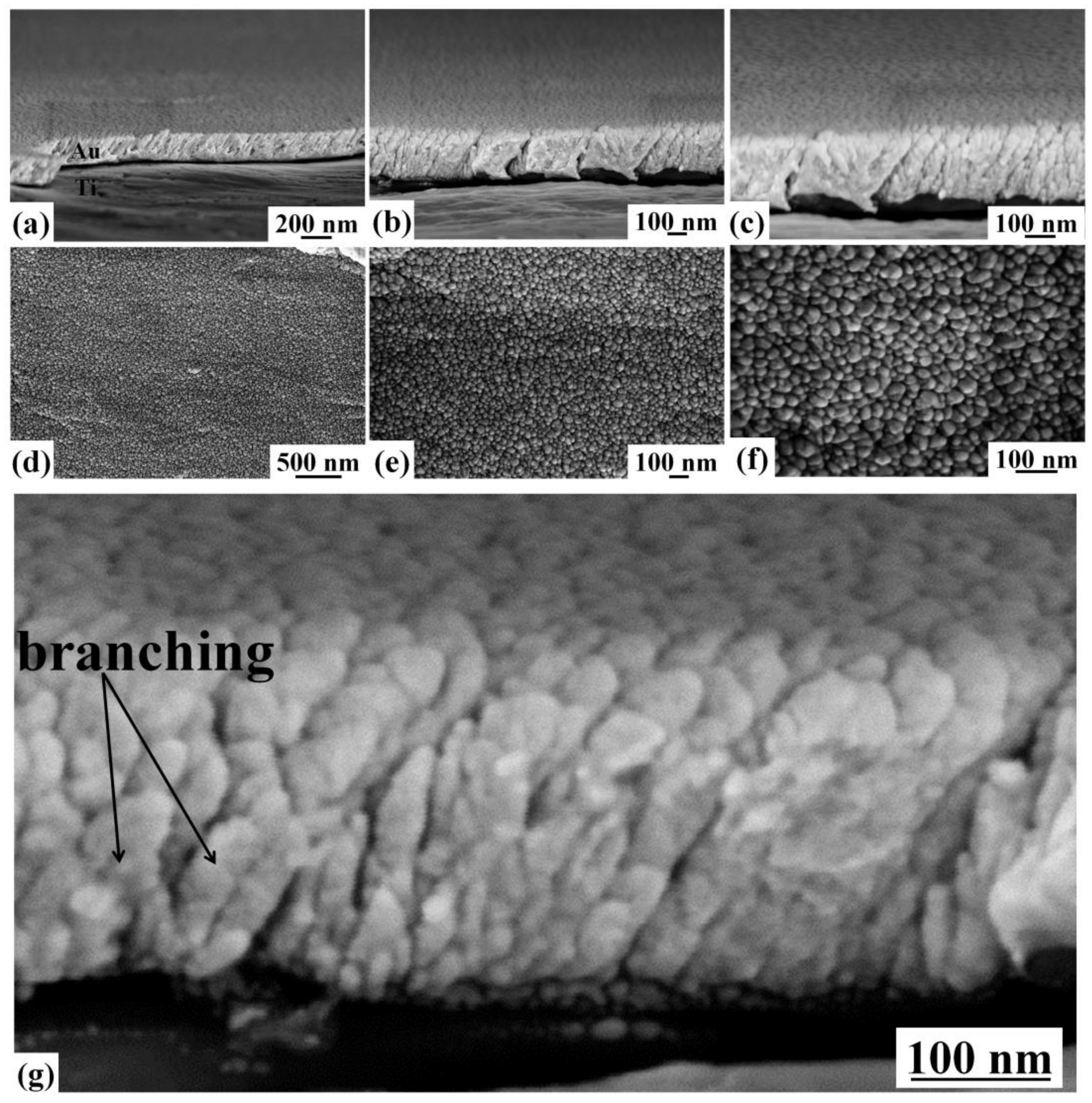
In fact [29], in the oblique deposition condition, the highest surface features geometrically shadow other surface regions from direct impingement by the incoming atoms from the vapor-phase (Figure 6). In the shadowed surface regions, adatoms can arrive only by indirect processes (vapor atoms reflection, scattering or desorption) or by surface diffusion from the other surface regions. The oblique angle deposition, so, by the self-shadowing effect, results in voided and low-density films. The result of such an effect is, also, the enhancement of the columnar morphology of the growing film, as we clearly observe for the thicker Au film deposited on Ti at θ = 48° (Figure 5). The adatoms surface diffusion length LD = quantifies the effect of the surface diffusion. In a similar way a shadowing length LS can be introduced to describe quantitatively the self-shadowing effect [32]. The capturing radius due to the shadowing increases with increasing the height h of the surface structures and the oblique angle θ so that LS = htanθ [31,32]. The final film morphology is dictated by the competition between LD and LS. LD is proportional to D/F (D the adatoms surface diffusivity and F the atoms impinging flux) and LS is proportional to the adatoms incidence angle θ. Our data in Figure 4 and Figure 5 show that the columnar morphology of the Au film is evident when it is deposited on the Ti substrate in the oblique incidence condition. This is particularly evident for the thicker Au film (Figure 5). Therefore, with respect to the Au film deposited in the normal incidence condition, in this case a less-dense film is obtained presenting an oblique-oriented columnar structure. In addition, the Au columns forming the film present a branched morphology (see Figure 5c) of the oblique-oriented columns forming the film. The branched morphology of the columns is due, according to Karabacak et al. [32], to the low adatom diffusivity D with respect to the vapor atoms impinging flux F, i.e., low value of D/F leading to metastable structures, since the adatoms are “frozen” in a spatial metastable configuration by the continuous arrival of new atoms from the vapor phase. The Monte Carlo-based simulations by Karabacak et al. [32] show that, in the oblique deposition condition, the branching of the growing columns is more and more enhanced as the adatoms surface diffusion rate is lower and lower (when fixed the atoms arrival rate). Our data are fully in agreement with these simulation results.
To further analyze the topographical differences in the four Au films on the basis of the thickness and deposition angle, we proceeded to the AFM analysis of the corresponding surfaces. In particular, these analyses allowed us to quantify the Au films surface roughness σ.
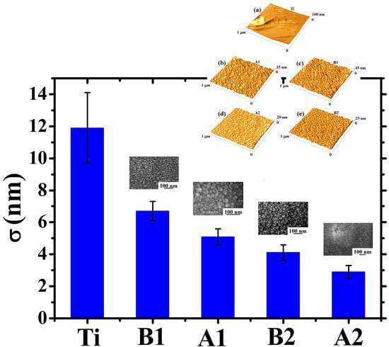
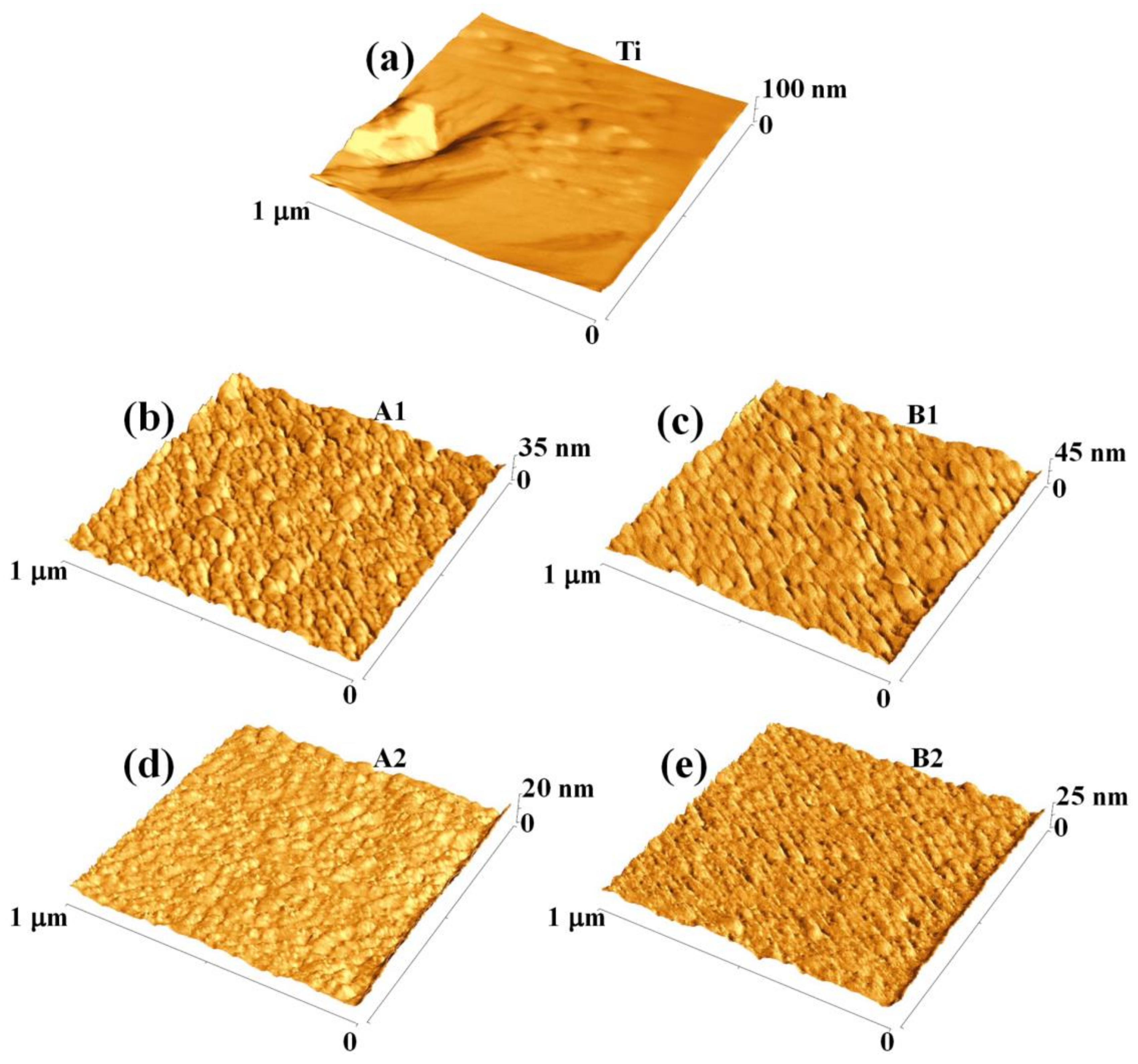
First of all, Figure 7 reports representative 1 μm × 1 μm AFM images (three-dimensional reconstructions) of the surface of: (a) bare Ti foil, (b) thinner (220 nm) Au film deposited, at normal incidence, on the Ti foil, (c) thinner (140 nm) Au film deposited, at oblique incidence, on the Ti foil, (d) thicker (350 nm) Au film deposited, at normal incidence, on the Ti foil, (e) thicker (230 nm) Au film deposited, at oblique incidence, on the Ti foil. The surface morphology of the Au film, in each case, resembles that evidenced by the SEM analysis for the corresponding sample. However, the AFM analysis give direct information on the height of the surface structures as evident from the three-dimensional AFM images reported in Figure 7: each images is accompanied by the z-scale (height scale). It is just evident the difference in the height scale for the bare Ti surface with respect to height scale of the samples having the Au film deposited on top. For the bare Ti surface the height scale ranges from 0 to 100 nm, in sample A1 from 0 to 35 nm, in sample B1 from 0 to 45 nm, in sample A2 from 0 to 20 nm, in sample B2 from 0 to 25 nm. Qualitatively, the 0-100 nm range in the height scale for the bare Ti sample is just an indication of a higher surface roughness with respect to the other samples since, in this sample, the height differences between valleys and peaks should be higher than in the other samples (as we will see in the following, the roughness parameter quantifies the vertical spacing of a surface, neglecting the horizontal spacing. If the vertical spacing are large, the surface is rough; if they are small the surface is smooth).
However, the AFM analyses allow quantitative evaluations on the Au films surface roughness. The roughness of a surface can be characterized by several parameters and functions [37,38,39,40]. The most used are the roughness average Ra and the Root Mean Square (RMS) width σ. They are defined, respectively, as Ra = <z(x,y)> and σ = <z(x,y)2>1/2 being z(x,y) = h(x,y) − <h(x,y)> with h(x,y) the height function and <z(x,y)> the spatial average over a planar reference surface [34,35,36,37,38,39,40]. Therefore, Ra is the arithmetic mean of the absolute values of the height of the surface profile. On the other hand, the RMS σ of a surface is similar to the roughness average Ra, with the only difference being the mean squared absolute values of surface roughness profile [40]. In particular, for the present analysis, we choose to characterize the surfaces roughness using the RMS (σ) parameter since it is more sensitive to surface peaks and valleys than Ra due to the squaring of the amplitude in its calculation [40]. We point out that there are two important factors which affect the resolution of the surface roughness measurement: the AFM instrument noise (which limits the vertical resolution), and the tip radius (which limits the spatial resolution). Regarding these aspects, we observe that: (i) the Bruker-Innova AFM instrument, thanks to the closed-loop measurement configuration, nominally, reaches a z noise floor <50 pm RMS, a closed-loop xy noise <1.2 nm RMS, and z linearizer noise <200 pm RMS [41]; (ii) we used, for the AFM measurements, Si tips with nominal radius of curvature of ~2 nm. Considering that the SEM analysis (Figure 2, Figure 3, Figure 4 and Figure 5) evidenced, in the analyzed samples, the formation of Au structures characterized by cross- and plan-dimensions (and spacing) much larger than these values, the following RMS analysis are not crucially affected by the instrument resolution limits.
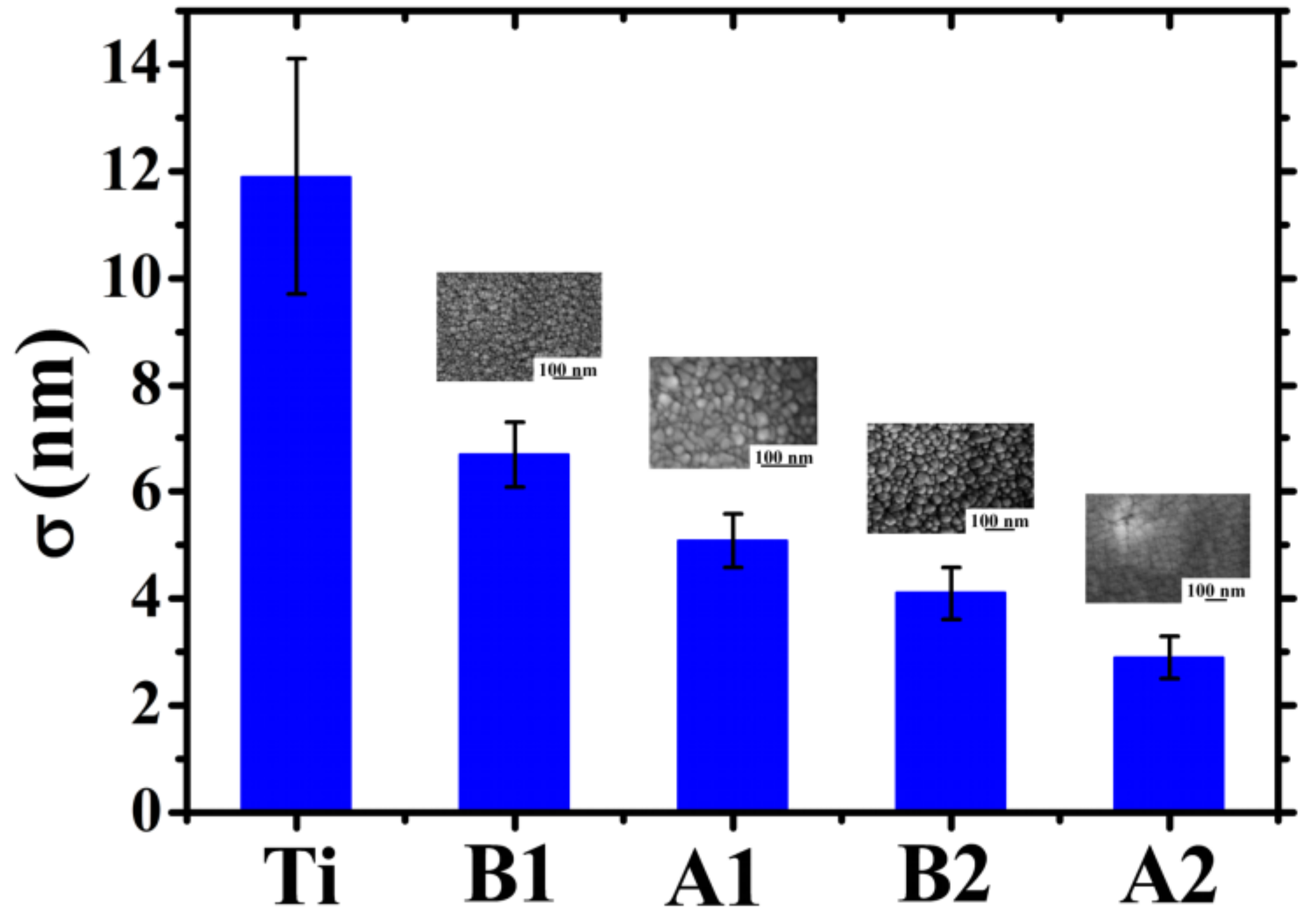
Therefore, for each sample, we acquired, at least, six AFM images per sample (1 μm × 1 μm). Using each image, the value σi of the roughness corresponding to that image was calculated by the SPMLABANALYSES V7.00 software. It calculates σi implementing a routine which evaluates σi = <z(x,y)2>1/2. Then, to each sample was associated the corresponding mean roughness σ as the mean value obtained by (at least) the six σi values. The error in σ was derived as the standard deviation arising from the averaging procedure. The results for all the samples, including the roughness of the starting Ti foil as reference, are summarized in the plot in Figure 8. Analyzing this plot, some conclusions can be drawn: (a) the starting Ti foil presents a high surface roughness (~12 nm). However, the Au deposit, in each case, has the effect to reduce the surface roughness.
This is due to the partial filling of the Ti surface holes determining, so, the decrease in the surface heights standard deviations. In other words, the Au film makes the surface more uniform in the sense that it decreases the surfaces height differences. (b) When fixed the deposition angle θ, the surface roughness σ decreases by increasing the Au film thickness (the roughness of sample A2 is lower than of sample A1, and the roughness of sample B2 is lower than of sample B1). This is due to the fact that depositing more and more Au atoms, the starting holes in the Ti substrate are more and more filled leading to the formation of a more and more flat surface. (c) When fixed the deposition time, the surface roughness σ increases by increasing the deposition angle θ. In fact, the increase of θ leads to the enhancement of the columnar morphology of the Au film, resulting in a more porous structure. Therefore, for θ = 0°, the compact Au film exhibits, on its surface, a low density of height discontinuities. On the contrary, for θ = 48°, the columnar morphology of the Au film greatly increases the surface density of height discontinuities (i.e., the separations between neighboring columns), resulting in the increase of the film surface roughness.
Summarizing, these data allow the tuning of the Au film structural characteristics for desired applications when a Ti adhesion layer is needed for the growth of the film. In fact:
- Applications which demand minimized surface roughness for the Au film [42,43], require thick Au films deposited in normal incidence condition. In this sense, for example, atomically flat Au films are needed for anchoring self-assembled organic monolayers (as examples hexadecanethiol self-assembled monolayers in [42] and tethered lipids in [43]) to fully exploit these systems as building blocks for molecular electronics or for sensing and bio-sensing devices [43]. In addition, the planar arrangement of the self-assembled organic monolayers on ultra-flat metal surfaces (Au in particular) allows the application of a variety of surface-analytical techniques for the overall characterizations of the molecules properties [43].
- Applications which demand high surface roughness for the Au film [44,45], require thin Au films deposited in oblique (i.e., glancing) deposition condition. In this sense, for example, recent years have seen an increasing interest in highly-efficient absorbers and scatterers of visible light for the conversion of solar energy into electrochemical energy. Regarding these applications, ultra-rough metal films can efficiently act, in a device, as light absorbing or scattering [44] and interference [45] elements with tuned action on the basis of roughness. Such capabilities are employed, for example, in plasmonic solar cells [44], broadband plasmonic absorbers [44], water splitting and photocatalysis devices [44], flexible optoelectronic devices [45].
- Applications which demand directional anisotropic properties (i.e., optical, electrical, etc.) of the Au film with minimized surface roughness [46,47], require thick Au film deposited in oblique deposition condition. On the contrary, the increase of the roughness can be obtained by reducing the film thickness. In this sense, for example, metal films presenting anisotropic elastic properties can be exploited for the production of innovative microelectrochemical devices [46]. In these films the elastic properties have a tensorial character resulting in direction-dependent response of the microelectrochemical devices [46]. On the other hand, for example, metal films with direction-dependent optical properties found recent interesting applications in devices exploiting the birefringence and dichroism effects on the nanoscale [47]. Some of these devices comprehend plasmon-assisted sensing and photovoltaic devices [47].
- Applications which demand high conductivity Au film [48], require compact and low-roughness film, i.e., thick films deposited in normal-incidence condition. In this sense, for example, the conductivity of thin metal film can be strongly different from the corresponding bulk material and determined by the porosity of the film [48]. The study of Smith et al. [48] shows that the resistance of deposited thin Au film can increase from about 10 Ω to about 108 Ω when in the film the Au volume fraction decreases from 1 to 0.16. This fact is crucial in realizing low-resistance Au metallizations for any devices requiring contacting electrodes.
- Applications which demand high-porous Au film [48,49,50], require film deposited in glancing condition. In this sense, for example, nanoporous Au films take advantage of their enormous exposed surface area to enhance chemical, electrochemical, and photoelectrochemical reactions (such as photoelectrochemical CO2 reduction [49], etc.).
A final comment related to Figure 8 concerns some comparisons with previous literature: in particular, the data in Figure 8 highlight an increase in the Au film surface roughness by increasing the deposition angle θ (when fixed the deposition time, so compare sample A1 to sample B1 and sample A2 to sample B2). A similar kinetic roughening was already observed in glancing angle deposition of metal films [51,52] and ascribed to the atomic shadowing effect that increases the growth rate of misoriented grains during growth. Dalla Torre et al. [51] sputter-deposited Ta films on inclined substrates and found an increase of the Ta surface roughness from about 1 nm to about 20 nm increasing the deposition angle from 0° to 85°. Frederick et al. [52] performed magnetron sputtering of CrN films on MgO(001) and found and CrN surface roughness increase from about 1 nm to about 10 nm increasing the deposition angle from 0° to 80°. Our data are fully consistent with these previous finding, however, in addition, highlight the strict connection of the surface roughness results to the cross-sectional nanoscale structure of the grown films.
4. Conclusions
We investigated the nanoscale plan and cross-section morphological characteristics of Au films sputter-deposited on Ti substrate both in normal and oblique conditions. We observed that both the cross-sectional and plan nanoscale structure as well as the surface roughness of the Au film change on the basis of the film thickness and deposition angle. In normal incidence condition, a compact, dense Au film is obtained showing, in addition, a resemblance of columnar morphology which is less evident increasing the film thickness. Furthermore, in this condition, increasing the film thickness, the film surface roughness decreases from about 5 nm (film thickness of 220 nm) to about 3 nm (film thickness of 350 nm). On the other hand, the oblique incidence condition enhances the branched columnar morphology of the film, leading to the formation of a porous film formed by well-distinguished columns which are tilted with respect to the normal direction to the substrate surface. Moreover, the oblique incidence condition leads to the increase of the film surface roughness (with respect to the normal incidence condition) but, also in this case, the surface roughness decreases by increasing the film thickness: the surface roughness decreases from about 7 nm (film thickness of 140 nm) to about 4 nm (film thickness of 230 nm).
Therefore, the data presented in this work can be useful in the in the establishment of a general scheme for the cross-sectional and plan structure of Au films used in devices where the use of Ti adhesion layer for Au is needed. Since these different nanoscale structures of the Au films can greatly influences the films physical properties, a general working framework relating the structural and physical properties could be set.
Author Contributions
F.R. and M.G.G. conceived and designed the experiments; F.R. performed the experiments and analyzed the data; F.R. and M.G.G. wrote the paper.
Conflicts of Interest
The authors declare no conflict of interest.
References
- Hass, G.; Francombe, M.H.; Vossen, J.L. Physics of Thin Films-Research and Development; Academic Press: New York, NY, USA, 1982. [Google Scholar]
- Zhigal’skii, G.P.; Jones, B.K. The Physical Properties of Thin Metal Films; Taylor and Francis: New York, NY, USA, 2003. [Google Scholar]
- Barmak, K.; Coffey, K. Metallic Films for Electronic, Optical and Magnetic Applocations-Structure, Processing and Properties; Woodhead Publishing Limited: Sawston, UK, 2014. [Google Scholar]
- Batra, I.P. Metallization and Metal-Semiconductor Interface; Plenum Press: New York, NY, USA, 1989. [Google Scholar]
- Wilson, S.R.; Tracy, C.J.; Freeman, J.L., Jr. Handbook of Multilevel Metallization for Integrated Circuits: Materials, Technology, and Applications; Noyes Publication: Norwich, NY, USA, 1993. [Google Scholar]
- Mattox, D.M. Thin film metallization of oxides in microelectronics. Thin Solid Films 1973, 18, 173–186. [Google Scholar] [CrossRef]
- Barth, J.V.; Costantini, G.; Kern, K. Engineering atomic and molecular nanostructures at surfaces. Nature 2005, 437, 671–679. [Google Scholar] [CrossRef] [PubMed]
- Vogt, K.W.; Kohl, P.A.; Carter, W.B.; Bell, R.A.; Bottomley, L.A. Characterization of thin titanium oxide adhesion layers on gold: Resistivity, morphology, and composition. Surf. Sci. 1994, 301, 203–213. [Google Scholar] [CrossRef]
- Nagata, H.; Shinriki, T.; Shima, K.; Tamai, M.; Haga, E.M. Improvement of bonding strength between Au/Ti and SiO2 films by Si layer insertion. J. Vac. Sci. Technol. A 1999, 17, 1018–1023. [Google Scholar] [CrossRef]
- Jupille, J.; Lazzari, R. Improving the wetting of oxides by metals. J. Optoelectr. Adv. Mater. 2006, 8, 901–908. [Google Scholar]
- Moazzez, B.; O’Brien, S.M.; Merschrod, E.F.S. Improved Adhesion of Gold Thin Films Evaporated on Polymer Resin: Applications for Sensing Surfaces and MEMS. Sensors 2013, 13, 7021–7032. [Google Scholar] [CrossRef] [PubMed] [Green Version]
- Cloud, T.A.; Houston, M.R.; Kohl, P.A.; Bidstrup, S.A. Evaluation of the processing and performance of noble metal MCMs. In Proceedings of the International Conference on Mutichip Modules Proceedings, ISHM, Denver, Colorado, 14–16 April 1993; p. 451. [Google Scholar]
- Aouani, H.; Wenger, J.; Gérard, D.; Rigneault, H.; Devaux, E.; Ebbesan, T.W.; Mahdavis, F.; Xu, T.; Blair, S. Crucial Role of the Adhesion Layer on the Plasmonic Fluorescence Enhancement. ACS Nano 2009, 3, 2043–2048. [Google Scholar] [CrossRef] [PubMed]
- Nilsson, S.; Klett, O.; Svedberg, M.; Amirkhani, A.; Nyholm, L. Gold-coated fused-silica sheathless electrospray emitters based on vapor-deposited titanium adhesion layers. Rapid Comm. Mass Spectr. 2003, 17, 1535–1540. [Google Scholar] [CrossRef] [PubMed]
- Habteyes, T.G.; Dhuey, S.; Wood, E.; Gargas, D.; Cabrini, S.; Schuck, P.J.; Alivisatos, A.P.; Leone, S.R. Metallic Adhesion Layer Induced Plasmon Damping and Molecular Linker as a Nondamping Alternative. ACS Nano 2012, 6, 5702–5709. [Google Scholar] [CrossRef] [PubMed]
- Reiss, G.; Brückl, H. The influence of surface roughness on electronic transport in thin films. Surf. Sci. 1992, 269, 772–776. [Google Scholar] [CrossRef]
- Jacob, U.; Vancea, J.; Hoffmann, H. Surface-roughness contributions to the electrical resistivity of polycrystalline metal films. Phys. Rev. B 1990, 41, 11852–11857. [Google Scholar] [CrossRef]
- Ke, Y.; Zahid, F.; Timoshevskii, V.; Xia, K.; Gall, D.; Guo, H. Resistivity of thin Cu films with surface roughness. Phys. Rev. B 2009, 79, 155406. [Google Scholar] [CrossRef]
- Tian, Z.-Q.; Ren, B.; Wu, D.-Y. Surface-Enhanced Raman Scattering: From Noble to Transition Metals and from Rough Surfaces to Ordered Nanostructures. J. Phys. Chem. B 2002, 106, 9463–9483. [Google Scholar] [CrossRef]
- Maradudin, A.A.; Méndez, E.R. Enhanced backscattering of light from weakly rough, random metal surfaces. Appl. Opt. 1993, 32, 3335–3343. [Google Scholar] [CrossRef] [PubMed]
- Bergström, D.; Powell, J.; Kaplan, A.F.H. The absorption of light by rough metal surfaces—A three-dimensional ray-tracing analysis. J. Appl. Phys. 2008, 103, 103515. [Google Scholar] [CrossRef]
- Stockman, M.I.; Bergman, D.J.; Anceau, C.; Brasselet, S.; Zyss, J. Enhanced Second-Harmonic Generation by Metal Surfaces with Nanoscale Roughness: Nanoscale Dephasing, Depolarization, and Correlations. Phys. Rev. Lett. 2004, 92, 057402. [Google Scholar] [CrossRef] [PubMed]
- Springer, J.; Poruba, A.; Müllerova, L.; Vanecek, M. Absorption loss at nanorough silver back reflector of thin-film silicon solar cells. J. Appl. Phys. 2004, 95, 1427–1429. [Google Scholar] [CrossRef] [Green Version]
- Goncher, G.M.; Parsons, C.A.; Harris, C.B. Photochemistry on rough metal surfaces. J. Phys. Chem. 1984, 88, 4200–4209. [Google Scholar] [CrossRef]
- Marmur, A. Wetting on Hydrophobic Rough Surfaces: To Be Heterogeneous or Not To Be? Langmuir 2003, 19, 8343–8348. [Google Scholar] [CrossRef]
- 348805 ALDRICH Titanium SIGMA-ALDRICH. Available online: http://www.sigmaaldrich.com/catalog/product/aldrich/348805?lang=it®ion=IT (accessed on 25 March 2018).
- Shah, P.J. Nanostructured Columnar Thin Films Using Oblique Angle Deposition: Growth, SERS Characterization and Litographic Processing. Ph. D. Thesis, Wright State University, Dayton, OH, USA, 2012. [Google Scholar]
- Abelmann, L.; Lodder, C. Oblique evaporation and surface diffusion. Thin Solid Films 1997, 305, 1–21. [Google Scholar] [CrossRef]
- Vick, D.; Friedrich, L.J.; Dew, S.K.; Brett, M.J.; Robbie, K.; Seto, M.; Smy, T. Self-shadowing and surface diffusion effects in obliquely deposited thin films. Thin Solid Films 1999, 339, 88–94. [Google Scholar] [CrossRef]
- Malac, M.; Egerton, R.F. Observations of the microscopic growth mechanism of pillars and helices formed by glancing-angle thin-film deposition. J. Vac. Sci. Technol. A 2001, 19, 158–166. [Google Scholar] [CrossRef]
- Ruffino, F.; Torrisi, V. Ag films deposited on Si and Ti: How the film-substrate interaction influences the nanoscale film morphology. Superlatt. Microstruct. 2017, 111, 81–89. [Google Scholar] [CrossRef]
- Karabacak, T.; Wang, G.-C.; Lu, T.-M. Quasi-periodic nanostructures grown by oblique angle deposition. J. Appl. Phys. 2003, 94, 7723–7728. [Google Scholar] [CrossRef]
- Tu, K.N.; Mayer, J.W.; Feldman, L.C. Electronic Thin Film Science; Macmilian Publishing Company: New York, NY, USA, 1992. [Google Scholar]
- Ruffino, F.; Crupi, I.; Irrera, A.; Grimaldi, M.G. Pd/Au/SiC Nanostructured Diodes for Nanoelectronics: Room Temperature Electrical Properties. IEEE Trans. Nanotechnol. 2010, 9, 414–421. [Google Scholar] [CrossRef]
- Ruffino, F.; Torrisi, V.; Marletta, G.; Grimaldi, M.G. Atomic force microscopy investigation of the kinetic growth mechanisms of sputtered nanostructured Au film on mica: Towards a nanoscale morphology control. Nanoscale Res. Lett. 2011, 6, 112. [Google Scholar] [CrossRef] [PubMed]
- Zhang, L.; Cosandey, F.; Persaud, R.; Madey, T.E. Initial growth and morphology of thin Au films on TiO2(110). Surf. Sci. 1999, 439, 73–85. [Google Scholar] [CrossRef]
- Barabasi, A.-L.; Stanley, H.E. Fractal Concepts in Surface Growth; Cambridge University Press: Cambridge, UK, 1995. [Google Scholar]
- Family, F.; Vicsek, T. Dynamics of Fractals Surfaces; World Scientific: Singapore, 1991. [Google Scholar]
- Ruffino, F.; Grimaldi, M.G.; Giannazzo, F.; Roccaforte, F.; Raineri, V. Atomic Force Microscopy Study of the Kinetic Roughening in Nanostructured Gold Films on SiO2. Nanoscale Res. Lett. 2009, 4, 262. [Google Scholar] [CrossRef] [PubMed]
- De Oliveira, R.R.L.; Albuquerque, D.A.C.; Cruz, T.G.S.; Yamaji, F.M.; Leite, F.L. Measurement of the Nanoscale Roughness by Atomic Force Microscopy: Basic Principles and Applications. In Atomic Force Microscopy-Imaging, Measuring and Manipulating Surfaces at the Atomic Scale; Bellitto, V., Ed.; INTECH: Rijeka, Croatia, 2012. [Google Scholar]
- The Best-Value Research AFM. Available online: https://www.bruker.com/products/surface-and-dimensional-analysis/atomic-force-microscopes/innova/overview.html (accessed on 25 March 2018).
- Jeong, W.; Lee, M.; Lee, H.; Lee, H.; Kim, B.; Park, J.Y. Ultraflat Au nanoplates as a new building block for molecular electronics. Nanotechnology 2016, 27, 215601. [Google Scholar] [CrossRef] [PubMed]
- Naumann, R.; Schiller, S.M.; Giess, F.; Grohe, B.; Hartman, K.B.; Kärcher, I.; Köper, I.; Lübben, J.; Vasilev, K.; Knoll, W. Tethered Lipid Bilayers on Ultraflat Gold Surfaces. Langmuir 2003, 19, 5435–5443. [Google Scholar] [CrossRef]
- Tan, F.; Li, T.; Wang, N.; Lai, S.K.; Tsoi, C.C.; Yu, W.; Zhang, X. Rough gold films as broadband absorbers for plasmonic enhancement of TiO2 photocurrent over 400–800 nm. Sci. Rep. 2016, 6, 33049. [Google Scholar] [CrossRef] [PubMed]
- Kats, M.A.; Capasso, F. Ultra-thin optical interference coatings on rough and flexible substrates. Appl. Phys. Lett. 2014, 105, 131108. [Google Scholar] [CrossRef]
- Faurie, D.; Djemia, P.; Le Bourhis, E.; Renault, P.-O.; Roussigné, Y.; Chérif, S.M.; Brenner, R.; Castelnau, O.; Patriarche, G.; Goudeau, P. Elastic anisotropy of polycrystalline Au films: Modeling and respective contributions of X-ray diffraction nanoindentation and Brillouin light scattering. Acta Mater. 2010, 58, 4998–5008. [Google Scholar] [CrossRef]
- Zhou, W.; Mandia, D.J.; Barry, S.T.; Albert, J. Anisotropic effective permittivity of an ultrathin gold coating on optical fiber in air, water and saline solutions. Opt. Express 2014, 22, 31665–31676. [Google Scholar] [CrossRef] [PubMed]
- Smith, G.B.; Maaroof, A.I.; Cortie, M.B. Percolation in nanoporous gold and the principle of universality for two-dimensional to hyperdimensional networks. Phys. Rev. B 2008, 78, 165418. [Google Scholar] [CrossRef]
- Song, J.T.; Ryoo, H.; Cho, M.; Kim, J.; Kim, J.-G.; Chung, S.-Y.; Oh, J. CO2 Reduction: Nanoporous Au Thin Films on Si Photoelectrodes for Selective and Efficient Photoelectrochemical CO2 Reduction. Adv. Energy Mater. 2017, 7, 1601103. [Google Scholar] [CrossRef]
- Jia, F.; Yu, C.; Deng, K.; Zhang, L. Nanoporous Metal (Cu, Ag, Au) Films with High Surface Area: General Fabrication and Preliminary Electrochemical Performance. J. Phys. Chem. C 2007, 111, 8424–8431. [Google Scholar] [CrossRef]
- Dalla Torre, J.; Gilmer, G.H.; Windt, D.L.; Kalyanaraman, R.; Baumann, F.H.; O’Sullivan, P.L.; Sapjeta, J.; Dìaz de la Rubia, T.; Djafari Rouhani, M. Microstructure of thin tantalum films sputtered onto inclined substrates: Experiments and atomistic simulations. J. Appl. Phys. 2003, 94, 263–271. [Google Scholar] [CrossRef]
- Frederick, J.R.; D’Arcy-Gall, J.; Gall, D. Growth of epitaxial CrN on MgO(001): Role of deposition angle on surface morphological evolution. Thin Solid Films 2006, 494, 330–335. [Google Scholar] [CrossRef]
Figure 1.
Scheme of the experimental setup for the Au depositions on Ti in normal condition (θ = 0°) or in oblique condition (θ = 48°).
Figure 1.
Scheme of the experimental setup for the Au depositions on Ti in normal condition (θ = 0°) or in oblique condition (θ = 48°).

Figure 2.
Cross-section ((a–c), with magnification increase from (a) to (c)) and plan-view ((d–g), with magnification increase from (d) to (g)) SEM images of the thinner (220 nm-thick) Au film deposited at θ = 0° on Ti (sample A1).
Figure 2.
Cross-section ((a–c), with magnification increase from (a) to (c)) and plan-view ((d–g), with magnification increase from (d) to (g)) SEM images of the thinner (220 nm-thick) Au film deposited at θ = 0° on Ti (sample A1).

Figure 3.
Cross-section ((a–c), with magnification increase from (a) to (c)) and plan-view ((d–f), with magnification increase from (d) to (f)) SEM images of the thicker (350 nm-thick) Au film deposited at θ = 0° on Ti (sample A2).
Figure 3.
Cross-section ((a–c), with magnification increase from (a) to (c)) and plan-view ((d–f), with magnification increase from (d) to (f)) SEM images of the thicker (350 nm-thick) Au film deposited at θ = 0° on Ti (sample A2).

Figure 4.
Cross-section ((a–c), with magnification increase from (a) to (c)) and plan-view ((d–f), with magnification increase from (d) to (f)) SEM images of the thinner (140 nm-thick) Au film deposited at θ = 48° on Ti (sample B1).
Figure 4.
Cross-section ((a–c), with magnification increase from (a) to (c)) and plan-view ((d–f), with magnification increase from (d) to (f)) SEM images of the thinner (140 nm-thick) Au film deposited at θ = 48° on Ti (sample B1).

Figure 5.
Cross-section ((a–c), with magnification increase from (a) to (c)) and plan-view ((d–f), with magnification increase from (d) to (f)) SEM images of the thicker (230 nm-thick) Au film deposited at θ = 48° on Ti (sample B2). (g) Reports a much higher magnification cross-view image to better highlight a branching phenomenon of the Au columns.

Figure 6.
Schematic picture illustrating the shadowing effect during the Au atoms deposition in the oblique condition and in the late state of the deposition process, when high Au surface structure are formed on the substrate surface. h is the characteristic height of these surface structures, θ the atoms deposition angle (angle for which the atoms from the vapor-phase arrive on the substrate surface), and LS the resulting shadowing length.

Figure 7.
1 μm × 1 μm three-dimensional AFM images of the surface of: (a) bare Ti foil; (b) thinner (220 nm) Au layer deposited, at θ = 0°, on Ti foil (sample A1); (c) thinner (140 nm) Au layer deposited, at θ = 48°, on Ti foil (sample B1); (d) thicker (350 nm) Au layer deposited, at θ = 0°, on Ti foil (sample A2); (e) thicker (230 nm) Au layer deposited, at θ = 48°, on Ti foil (sample A2).

Figure 8.
Plot synthesizing the comparison of the roughness σ for the bare Ti surface, of the surface of the thinner (140 nm) Au film deposited, at θ = 48°, on Ti foil (sample B1), thinner (220 nm) Au film deposited, at θ = 0°, on Ti foil (sample A1), thicker (230 nm) Au film deposited, at θ = 48°, on Ti foil (sample B2), thicker (350 nm) Au film deposited, at θ = 0°, on Ti foil (sample A2).


Table 1.
Summary of the deposition conditions (deposition angle and deposition time) of the Au films and resulting thickness of the Au films. The first column reports the names assigned to the samples.
Table 1.
Summary of the deposition conditions (deposition angle and deposition time) of the Au films and resulting thickness of the Au films. The first column reports the names assigned to the samples.
| Sample | Deposition Angle θ (°) | Deposition Time (min) | Au Film Thickness h (nm) |
|---|---|---|---|
| A1 | 0 | 20 | 220 |
| A2 | 0 | 32 | 350 |
| B1 | 48 | 20 | 140 |
| B2 | 48 | 32 | 230 |
© 2018 by the authors. Licensee MDPI, Basel, Switzerland. This article is an open access article distributed under the terms and conditions of the Creative Commons Attribution (CC BY) license (http://creativecommons.org/licenses/by/4.0/).
Share and Cite
MDPI and ACS Style
Ruffino, F.; Grimaldi, M.G. Morphological Characteristics of Au Films Deposited on Ti: A Combined SEM-AFM Study. Coatings 2018, 8, 121. https://doi.org/10.3390/coatings8040121
AMA Style
Ruffino F, Grimaldi MG. Morphological Characteristics of Au Films Deposited on Ti: A Combined SEM-AFM Study. Coatings. 2018; 8(4):121. https://doi.org/10.3390/coatings8040121
Chicago/Turabian StyleRuffino, Francesco, and Maria Grazia Grimaldi. 2018. "Morphological Characteristics of Au Films Deposited on Ti: A Combined SEM-AFM Study" Coatings 8, no. 4: 121. https://doi.org/10.3390/coatings8040121
Note that from the first issue of 2016, this journal uses article numbers instead of page numbers. See further details here.