Electronic Structure Characterization of Hydrogen Terminated n-type Silicon Passivated by Benzoquinone-Methanol Solutions


1
Department of Chemistry and Biochemistry, University of Delaware, Newark, DE 19716, USA
2
Department of Materials Science and Engineering, University of Delaware, Newark, DE 19716, USA
*
Author to whom correspondence should be addressed.
Coatings 2018, 8(3), 108; https://doi.org/10.3390/coatings8030108
Submission received: 10 January 2018
/
Revised: 14 March 2018
/
Accepted: 16 March 2018
/
Published: 17 March 2018
(This article belongs to the Special Issue Advanced Surface Passivation Processes for Solar Cells)
Abstract
:The electrical passivation mechanism of benzoquinone-methanol solutions on silicon has been examined through the study of the silicon surface electronic structure. Surface photovoltage (SPV) measurements using both X-ray photoelectron spectroscopy (XPS) and scanning Kelvin probe microscopy (SKPM) indicate a downward band bending of H-Si and benzoquinone (BQ) and methanol (ME) treated samples. This suggests the creation of an accumulation layer of majority carriers near the surface, with a significant field-effect contribution to the observed surface passivation. The highest SPV values recorded for the ME-Si and BQ-Si samples of about −220 mV are approaching the Fermi level—conduction band crossover. Density functional theory (DFT) calculations show that a dipole is formed upon bonding of BQ radicals on the surface, decreasing the surface electron affinity and work function. Considering the 0.07 eV shift due to the dipole and the 0.17 eV downward band bending, the work function of BQ-Si is found to be 4.08 eV. Both the dipole and downward band bending contribute to the formation of surface electron accumulation, and decrease the minority carrier density of n-Si passivated by BQ.
1. Introduction
Silicon is the dominant material in photovoltaic devices, and the treatment of silicon surfaces to reduce harmful surface recombination effects is crucial to Si-based device performance. The conventional SiNx, SiO2, and Al2O3 surface passivation methods require capital expensive processes like ALD (atomic layer deposition) and PECVD (plasma-enhanced chemical vapor deposition) [1]. Room-temperature solution-based organic passivation methods, however, can provide alternatives with a much lower CapEx (capital expenditure).
Benzoquinone in methanol solutions (BQ/ME) is one of the organic passivants that has been utilized as a temporary passivant for hydrogen terminated silicon surfaces, providing a surface recombination velocity as low as 1.6 cm/s, in equivalent to the existing thin film passivation techniques like SiNx, SiO2, and Al2O3 [1,2,3,4,5,6]. Previous work in our group has found that the chemical passivation mechanism is radical-driven and light sensitive, where the semiquinone radical QH•, C6H4–OH–O•, and methanol radical CH3O• are responsible for bonding to the silicon surface defect sites resulting in a reduction of interface states [6,7]. Presumably, bonding of BQ and ME groups on n-Si surfaces can also affect the electron distribution, which may introduce an electrical passivation effect. Cahen et al. [5] have reported that the negatively charged benzene bonding on n-Si pulls electrons away from the Si space charge region, and inverts the surface to p-type, based on the observations from vibrating Kelvin probe. However, this work, verified by both scanning Kelvin probe microscopy (SKPM) and X-ray photoelectron spectrometer (XPS), is contrary to the results of Cahen et al., suggesting that the BQ/ME treated n-Si surface accumulates electrons (n++ type).
The work function is the key to explore the electronic structure of BQ modified Si surface, which is determined by a combination of the surface band bending and electron affinity [8,9]. Band bending can be induced by metals–semiconductor contact, surface states, adsorption, and field effect [10,11,12]. In the case of solution passivation, like benzoquinone-methanol (BQ/ME) passivation, band bending may exist on Si surfaces due to the different chemical environment between surface and bulk, such as the termination of lattice periodicity at the surface, absorption of molecules, or contact with other materials [5,12,13,14]. Band bending can be probed with the surface photovoltage (SPV) technique. The SPV measurement is a contactless and non-destructive technique to characterize band bending by measuring light induced changes on the semiconductor surfaces [13,14]. In SPV measurements, when a semiconductor is excited by light with sufficient energy, the absorbed photons will generate electron–hole pairs. The generated carriers push the system to flat-band conditions [15]. Therefore, the extent of band bending can be probed by changing the illumination conditions. Band bending at solid interfaces can be estimated with the Kelvin probe method where the contact potential difference (CPD) between the Si sample and metal tip is recorded under different illumination conditions. SPV can also be measured using photoelectron spectroscopy, where SPV is calculated by the changes of valence/core level electron binding energies.
The second component of the work function is the surface electron affinity χ. A dipole induced by an adsorbed polar molecule can alter the surface electron affinity and result in a change in the work function. The dipole contribution can be independently determined through density functional theory (DFT) calculations [16]. Since DFT calculations do not include doping and, therefore, the band-bending component of the work function is not included, then the difference in the calculated work function Φ can be attributed to the dipole δ, Equation (1).
In this study, the conduction and valence band bending on BQ and methanol treated n-type silicon surfaces will be characterized using both Kelvin probe and X-ray photoelectron spectroscopy (XPS). The surface dipole will be calculated using DFT in the Vienna ab initio simulation package (VASP). The work function of the BQ-Si surface relative to the H-Si surface can then be calculated from the band bending and dipole behaviors.
2. Materials and Methods
The wafers used in this work were double side polished n-type silicon (100) FZ wafers with a resistivity of 1–5 Ω·cm and 280 ± 20 µm thickness.
The following cleaning procedure was used for every trial to achieve hydrogen termination: The first step was a piranha clean consisting of a 5-min bath in a 4:1 solution of sulphuric acid and hydrogen peroxide. Piranha solutions were freshly made and cooled at room temperature for 10 min before use. Subsequently, the wafers were given a 5-min DI water submersion and then followed by a 2-min HF (2%) immersion. These H-Si wafers were then briefly rinsed with DI water and blown dry with N2.
The cleaned H–Si wafers were quickly placed in a sealed plastic bag containing a 0.01 mol/L BQ/ME solution or pure methanol solution to achieve BQ or ME termination. Samples were kept in BQ/ME for 1 h and 24 h in ME before SPV testing for an optimal passivation effect based on the immersion time study [6].
SPV was measured using a Physical Electronics (Chanhassen, MN, USA) model 5600 X-ray photoelectron spectrometer (XPS) with an overall accuracy of 0.05 eV. A 300 W xenon lamp was used for illumination, where the light was focused on the sample surface through a quartz window on the XPS chamber. Silicon samples were grounded with carbon tape on the stage. The XPS chamber was kept in ultra-high vacuum and cooled to around 17 °C.
A scanning Kelvin probe microscopy (SKPM), equipped with an Asylum Research (Santa Barbara, CA, USA) MFP-3D atomic force microscope (AFM) was also used to study SPV. The silicon tips coated with Pt were calibrated with freshly peeled HOPG (highly ordered pyrolytic graphic). A 650 nm red laser with a power output of 20 mW was used for charger carrier excitation. Measurements were taken under nitrogen purge in ambient room condition.
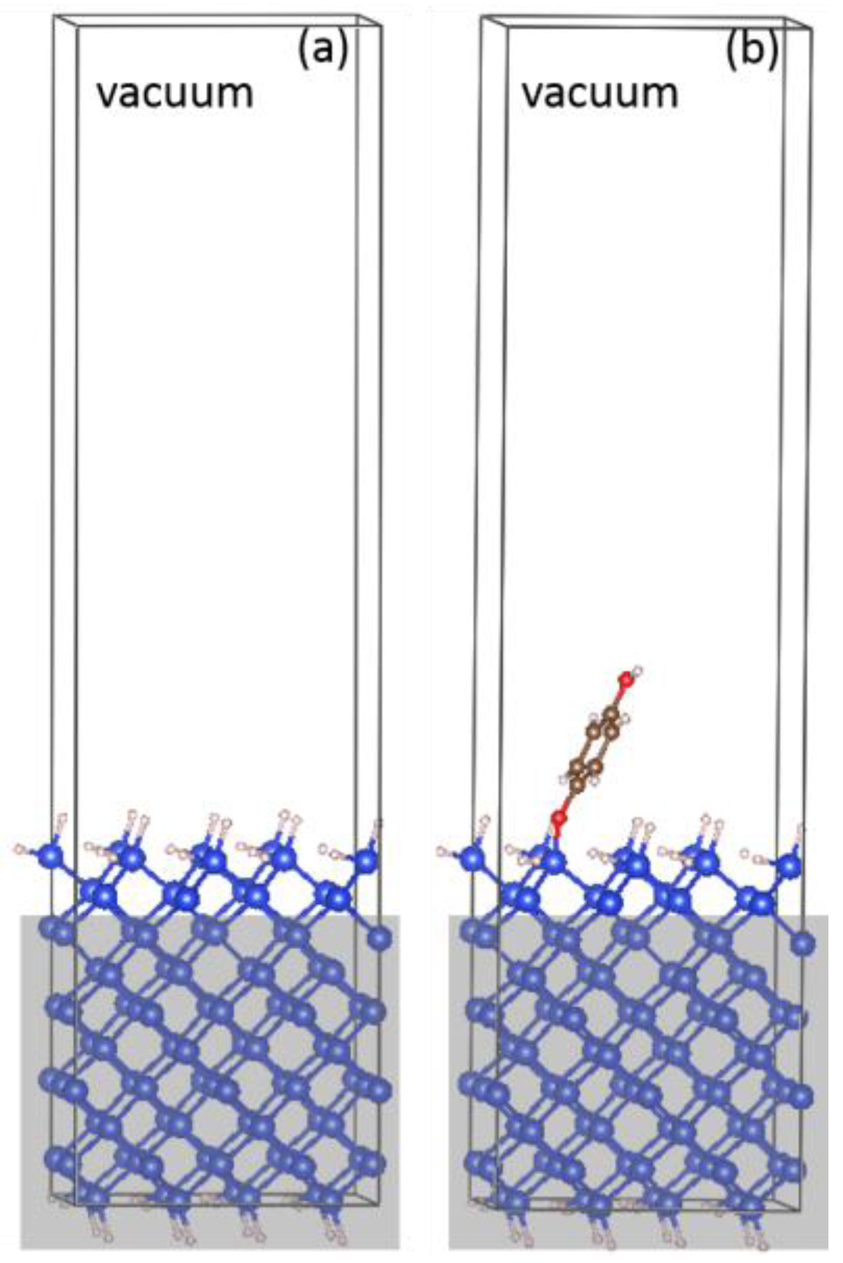
Dipole calculations were performed for a dihydride-passivated and a BQ-adsorbed Si(100) surface using the Vienna ab initio simulation package (VASP) [17]. The interaction between ions (nuclei) and electrons were described using projector augmented wave pseudopotentials [18]. Electron–electron exchange and correlation interactions were described using the gradient corrected Perdew–Burke–Ernzerhof (PBE) functional [19]. The Brillouin-zone (BZ) integrations were performed using the Monkhorst–Pack (4 × 4 × 1) K-point set. The unit cell was a 4 × 4 periodic slab containing 10 atomic layers. The coordinates of the Si atoms in the bottom eight layers of Si were kept fixed after silicon slab relaxation. The vacuum region was approximately 25 Å. The energy cut-off of 400 eV was chosen based on energy dependence study of cutoff energy from 350 to 600 eV. For the H-terminated Si, all top and bottom layer silicon atoms were terminated with two hydrogen atoms per silicon, as shown in Figure 1a. This 1 × 1 canted-row dihydride structure is found to be energetically favorable with respect to the symmetric 1 × 1 dihydride, in good agreement with literature [20]. For the BQ-adsorbed Si, one of the two hydrogens adsorbed on Si was replaced by a BQ radical, QH•, per unit cell, as shown in Figure 1b [6]. The coverage of QH• was one QH• per eight surface Si atoms. Absorption of BQ is chosen to happen only on the front surface of the silicon to match the surface measurements in Kelvin probe and XPS [21].
3. Results
3.1. SPV Measurements by XPS
Band bending on three n-type Si(100) wafers were studied via XPS: H-terminated Si (H-Si), BQ/ME passivated Si (BQ-Si) and methanol treated Si (ME-Si). The hydrogen termination was achieved by using the piranha/HF cleaning procedure described in the experimental section. BQ-Si and ME-Si were achieved by immersing H-Si in BQ/ME or ME solution for 1 h and 24 h respectively before testing, based on the immersion time study where the BQ/ME is observed reaching the highest passivation in 1 h, and ME passivation takes 24 h [6].
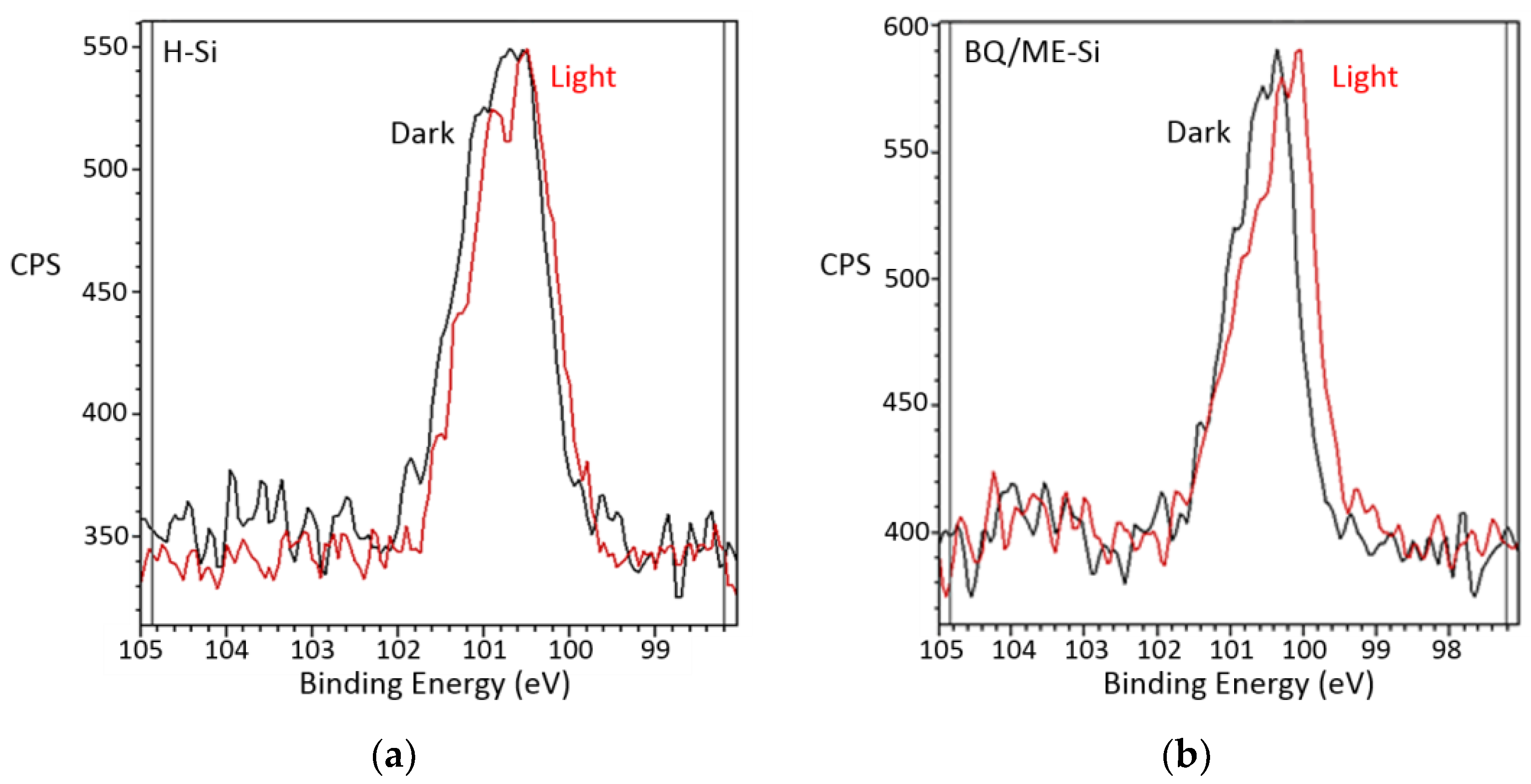
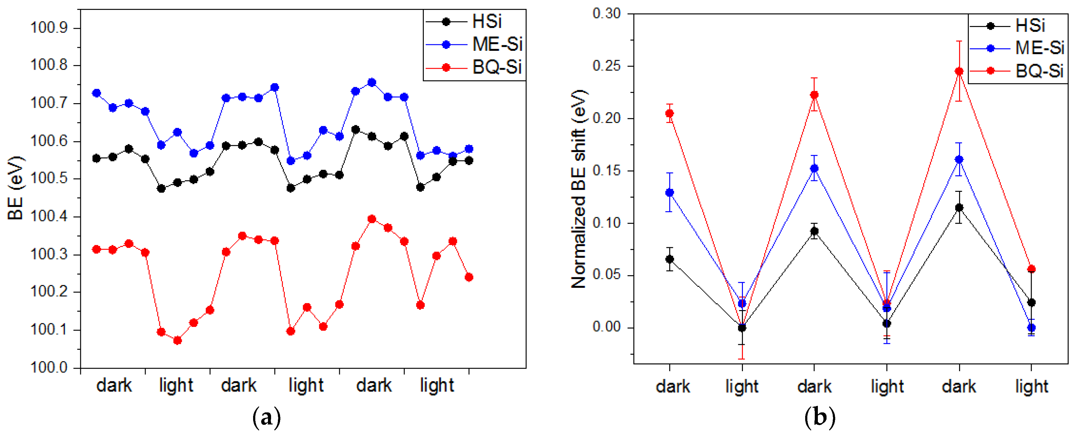
Figure 2 shows the shift of Si 2p peak of H terminated Si and BQ treated Si with xenon light on and off. Si 2p shifts to lower binding energy on both samples in the light condition, while BQ/ME-Si shifts more than the H-Si sample. Repetitive light and dark conditions were performed on Si samples with three different treatments, recorded in Figure 3. It can be seen that a repeatable energy shift to lower binding energy in the illumination condition exists on all three samples, which indicates a downward band bending.
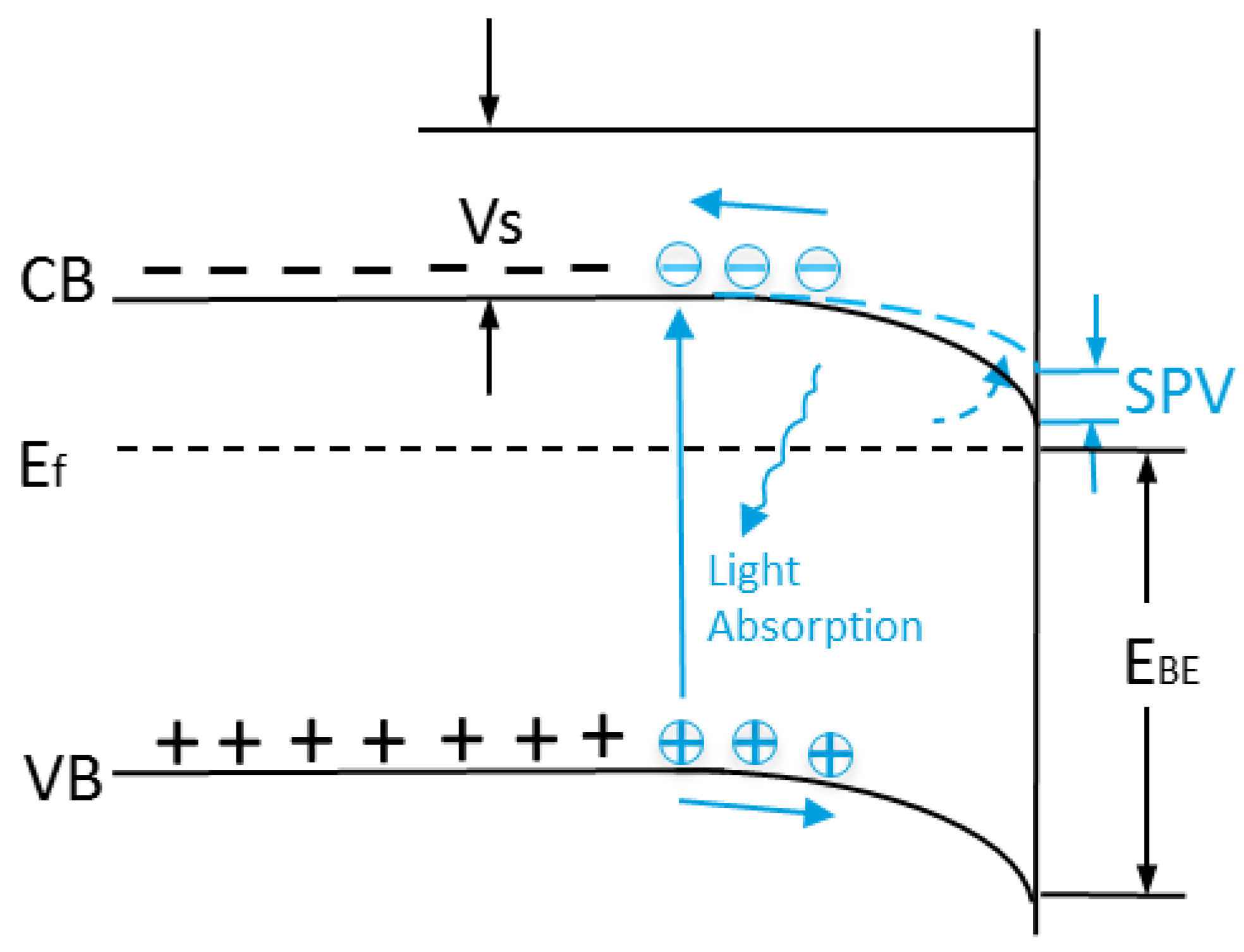
In a downward band bending scheme, shown in Figure 4, the light generated carriers compensate the built-in potential Vs, and the measured EBE decreases. This observed downward band bending indicates that BQ/ME bonding to the silicon surface introduces an electron accumulation layer on the surface, causing a decrease in minority carrier density at the surface and an increase in passivation. The SPV is 230 ± 50 meV on BQ/ME treated n-type Si, and followed by ME-Si and H-Si, which suggests that the stronger field effect of BQ/ME can contribute to a longer lifetime [6].
3.2. SPV Measurements by SKPM
n-type Si(100) wafers with three different surface treatments—H-Si, BQ-Si, and ME-Si as described in the previous section—were studied in SKPM. The contact potential difference (CPD) between the Kelvin probe tip and the grounded samples’ surface were recorded in a scan size of 3 µm × 3 µm, shown in Figure 5. An initial scan found high spatial homogeneity of the contact potential difference, with less than 5 mV of variation across the area of the sample.
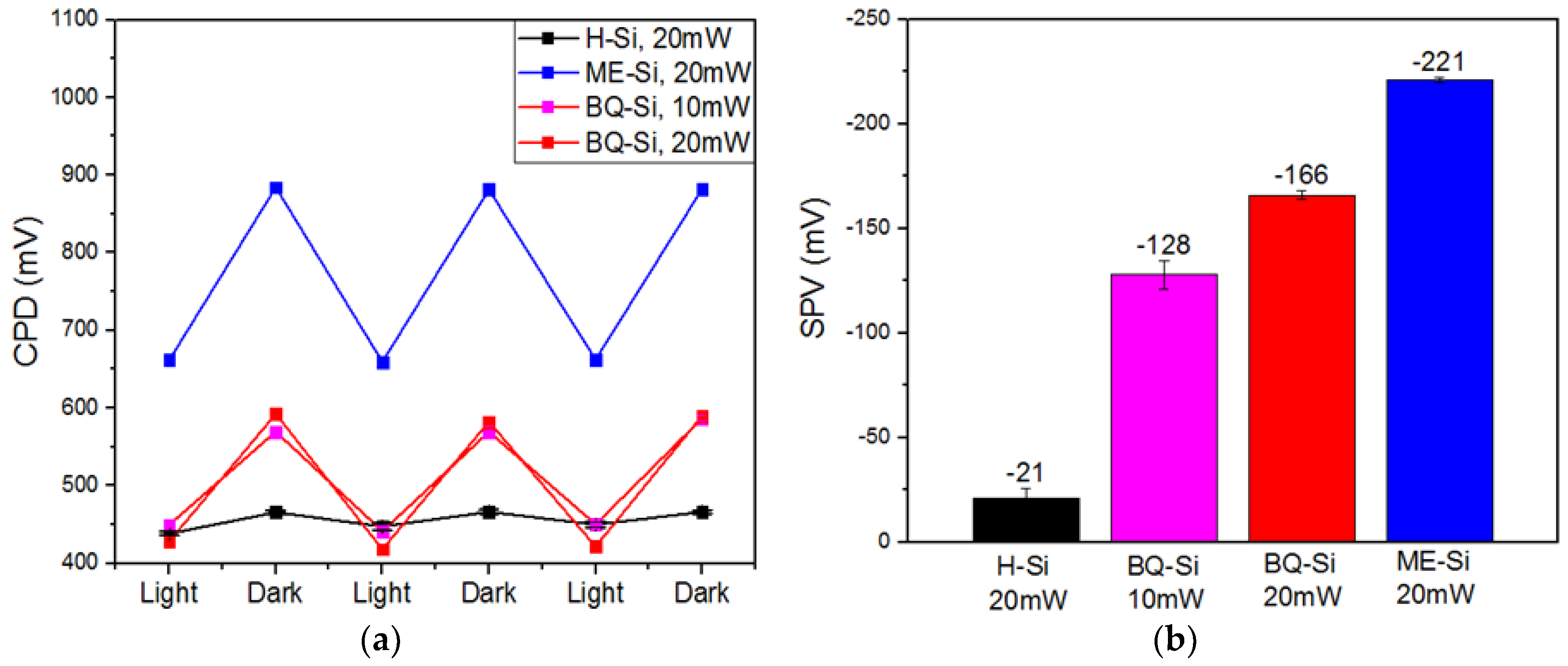
For all samples, a reproducible shift of CPD is observed when the 650 nm light source is switched on and off during the scan. The average CPD values in each 0.5 µm × 3 µm region are reported relative to the HOPG reference in Figure 6a. It can be seen that the shift in potential between the light and dark conditions is consistent across the area of each sample with an error bar smaller than 5 mV. Comparing the 10 mW (depicted in red) and 20 mW (depicted in blue) light irradiation on BQ-Si, both reach an illuminated CPD of around 450 mV. This suggests that the 20 mW 650 nm laser illumination is close to approaching a flat-band condition of around 450 mV on this sample. Similar results are found for the H-Si sample. However, the illuminated CPD of the ME-Si surface is observed to be 200 mV higher. This could be explained by a change in grounding or differing surface dipoles between the treatments, but would not affect the magnitude of the surface photovoltage.
Surface photovoltage (SPV) is obtained by calculating the difference of CPD between light and dark conditions, shown in Figure 6b. The negative SPV values confirm a downward band bending for n-type Si with all three surface treatments. However, band bending on ME-Si is observed higher than BQ-Si, in contrast to the XPS results, which might be caused by the interference of oxygen oxidization on BQ-Si caused by inefficient N2 purge.
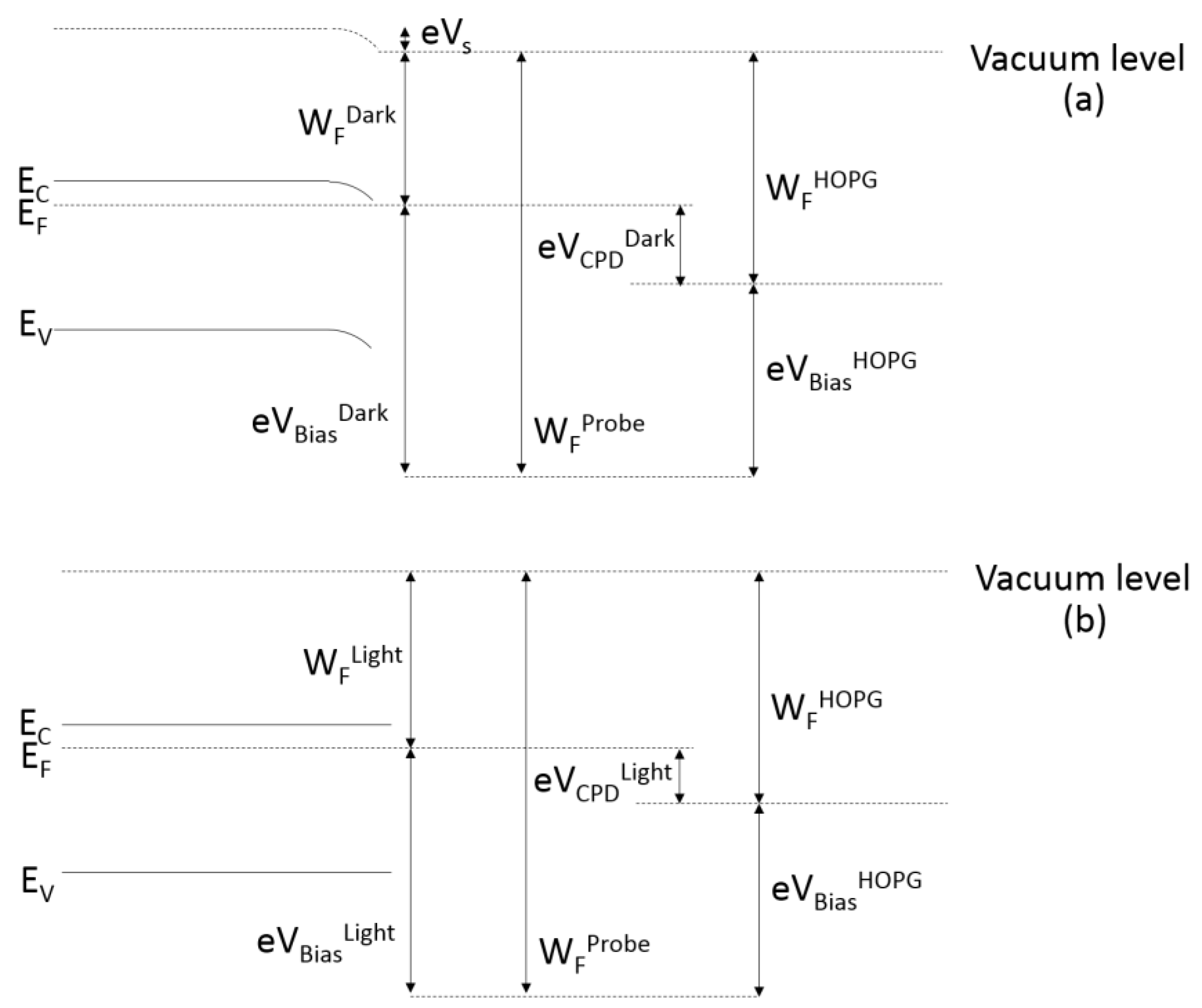
The energy levels measured in dark and light condition in Kelvin probe are illustrated in Figure 7. The applied bias voltage VBias is equal to the difference in work functions of the probe (WFProbe) and sample (WFLight or WFDark). To remove the effect of the unknown probe work function, the contact potential difference VCPD is reported relative to the bias measured on an HOPG reference sample. The difference in VCPDLight and VCPDDark gives the surface photovoltage, SPV. The work function of the BQ passivated n-Si surface is thus found out to be 4.15 eV.
With SKPM, it further confirms that immersing H terminated Si in BQ and ME solutions increases the downward band bending, which agrees with the band bending reported by XPS in Figure 3. Additionally, the work function of the BQ passivated n-Si surface is calculated to be around 4.15 eV by SKPM.
3.3. Surface Dipole and Work Function Calculation
The second component of the work function is the surface electron affinity χS, which is defined as the energy required to excite a surface electron from the bottom of the conduction band to the local vacuum level [22]. The surface dipole (δ) equals the difference between the surface electron affinity χS and the bulk electron affinity χB (4.05 eV for χB), shown in Equation (2) [23,24]. Depending on the dipole size and direction, the molecular dipole can increase or decrease χS. A negative dipole with respect to surface normal decreases χS and Φ because an emitted electron is accelerated within this dipole field on its way from the conduction band at the surface into the local vacuum, and vice versa.
Surface dipoles introduced by the bonding of the BQ radical were calculated using VASP. The computed electrostatic potential difference is the change in the surface dipole component of the work function, since the potential contribution from the bulk to the work function remains the same for both H-Si and BQ-Si surfaces. In VASP, the work function Φ is the difference between the vacuum potential Evac and Fermi level εF
The calculated electrostatic potential profiles for H-Si and BQ-Si surfaces are shown in Figure 8. A decrease in work function due to a negative surface dipole δ = −0.07 eV upon BQ adsorption is observed. The negative dipole energy shift observed agrees with our previous DFT calculation in Gaussian where the BQ bonding group was shown to be an electron-rich system [6].
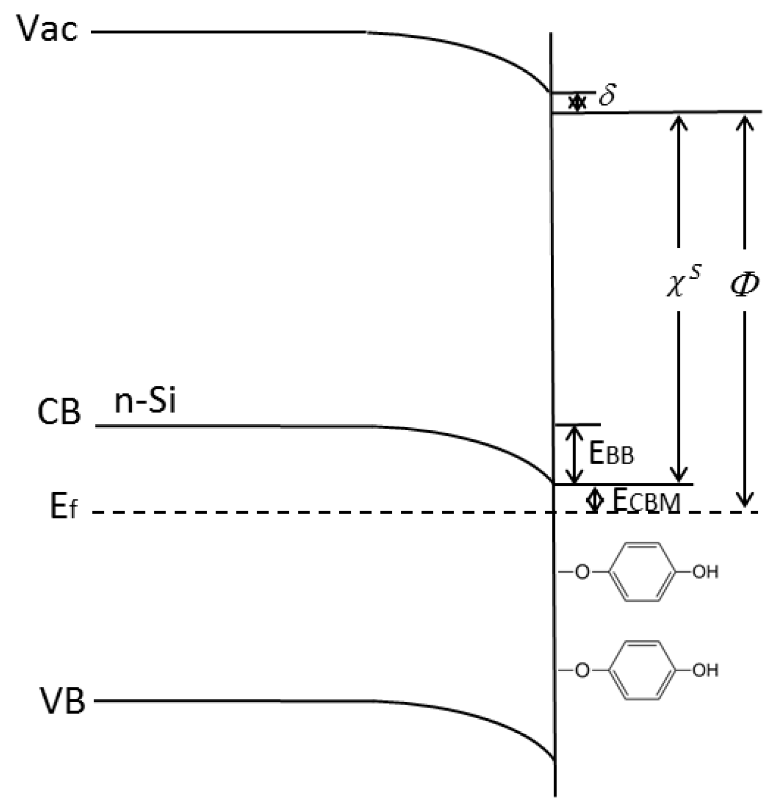
The work function of the BQ passivated n-Si surface, shown in Figure 9, can thus be calculated using the equations
where CB − εF = −0.27 eV is based on the Si doping level of 1015 cm−13, and the band bending energy EBB = 0.17 eV is obtained from the SKPM results in Figure 6. The work function of the BQ passivated n-Si surface is thus found out to be 4.08 eV, in close agreement with the 4.15 eV found in SKPM when using HOPG as a reference. It should be noted that the coverage of QH• simulated here is larger than experimental coverage, and QH• bonding is not the only component of the surface dipole, methanol, oxidation, and other surface irregularities contribute to the experimentally measured value of the surface dipole as well. The electronic structure of BQ passivated n-Si surfaces in Figure 9 further explains the BQ passivation mechanism, where both the negative dipole δ and the downward band bending EBB contribute to the decrease of the Si surface work function, resulting in accumulation, a more electron-rich surface. With the chemical bonding mechanism found in previous work [6], we conclude that BQ passivation on n-Si decreases the surface defect states, as well as forms an electron accumulation layer, decreasing the minority carrier density on the surface.
4. Discussion and Conclusions
Surface photovoltage measurements via both the photoemission and SKPM techniques indicate a downward band bending of H-Si and BQ and ME treated samples. This suggests the creation of an accumulation layer of majority carriers near the surface, with a significant field-effect contribution to the observed surface passivation. It is seen that subsequent treatment of hydrogen terminated Si with solutions of methanol and benzoquinone further increases the magnitude of band bending. It is expected that variations between samples in the amount of oxide formation at the surface could explain some of the variation in SPV values recorded between the two measurement methods. The highest SPV values recorded for the ME-Si and BQ-Si samples of about −220 mV are approaching the Fermi level–conduction band crossover. The similar magnitudes of surface band bending observed with both the BQ-ME and ME treatments are consistent with the expected mechanism of the surface modification, in which both BQ radicals and methanol radicals adhering to the surface [6]. This work, verified by two measurement techniques, is contrary to the suggestion of Cahen et al. that BQ-Si exhibits an upward band-bending, suggesting a different method of field-effect passivation [5].
DFT calculations show that a negative dipole is formed upon bonding of BQ radicals on the surface, decreasing the surface electron affinity and work function. Considering the 0.07 eV shift due to the negative dipole δ and the 0.17 eV downward band bending EBB, the work function of BQ-Si is found to be 4.08 eV, in agreement with SKPM results. Both the negative dipole and downward band bending contribute to the formation of electron accumulation on n-Si passivated by BQ.
With the chemical bonding mechanism found in previous work [6], we can conclude BQ passivation on n-Si mechanism, that BQ radicals bonding on n-Si decreases the surface defect states, as well as forms an electron accumulation layer, decreasing the minority carrier density on the surface.
Acknowledgments
This material is based upon work supported primarily or in part by the Engineering Research Center Program of the National Science Foundation and the Office of Energy Efficiency and Renewable Energy of the Department of Energy under NSF Cooperative Agreement No. EEC-1041895. Any opinions, findings and conclusions or recommendations expressed in this material are those of the author(s) and do not necessarily reflect those of the National Science Foundation or Department of Energy.
Author Contributions
Robert L. Opila and Meixi Chen conceived and designed the SPV experiments. Meixi Chen and Xi Lin designed and performed the SPV-XPS experiments; Meixi Chen and James H. Hack designed and performed the SPV-SKPM experiments; Meixi Chen and Anderson Janotti analyzed the DFT data; Robert L. Opila and Meixi Chen contributed to the overall data interpretation; Meixi Chen, James H. Hack and Robert L. Opila wrote the paper.
Conflicts of Interest
The authors declare no conflict of interest. The founding sponsors had no role in the design of the study; in the collection, analyses, or interpretation of data; in the writing of the manuscript, and in the decision to publish the results.
References
- Bakke, J.R.; Pickrahn, K.L.; Brennan, T.P.; Bent, S.F. Nanoengineering and interfacial engineering of photovoltaics by atomic layer deposition. Nanoscale 2011, 3, 3482–3508. [Google Scholar] [CrossRef] [PubMed]
- Takato, H.; Sakata, I.; Shimokawa, R. Surface passivation of silicon substrates using quinhydrone/methanol treatment. In Proceedings of the 3rd World Conference on Photovoltaic Energy Conversion, Osaka, Japan, 11–18 May 2003; Volume 2, pp. 1108–1111. [Google Scholar]
- Takato, H.; Sakata, I.; Shimokawa, R. Quinhydrone/methanol treatment for the measurement of carrier lifetime in silicon substrates. Jpn. J. Appl. Phys. 2002, 41, L870–L872. [Google Scholar] [CrossRef]
- Watanabe, N.; Kondo, Y.; Ide, D.; Matsuki, T.; Takato, H.; Sakata, I. Characterization of polycrystalline silicon wafers for solar cells sliced with novel fixed-abrasive wire. Prog. Photovolt. Res. Appl. 2010, 18, 485–490. [Google Scholar] [CrossRef]
- Har-lavan, R.; Schreiber, R.; Yaffe, O.; Cahen, D. Molecular field effect passivation: quinhydrone/methanol treatment of n-Si(100). J. Appl. Phys. 2013, 113, 084909. [Google Scholar] [CrossRef]
- Chen, M.; Hack, J.H.; Iyer, A.; Jones, K.J.; Opila, R.L. Radical-driven silicon surface passivation by benzoquinone-, hydroquinone-methanol and photoinitiators. J. Phys. Chem. C 2017, 121, 21364–21373. [Google Scholar] [CrossRef]
- Kotulak, N.A.; Chen, M.; Schreiber, N.; Jones, K.; Opila, R.L. Examining the free radical bonding mechanism of benzoquinone- and hydroquinone-methanol passivation of silicon surfaces. Appl. Surf. Sci. 2015, 354, 469–474. [Google Scholar] [CrossRef]
- He, T.; Ding, H.; Peor, N.; Lu, M.; Corley, D.A.; Chen, B.; Ofir, Y.; Gao, Y.; Yitzchaik, S.; Tour, J.M. Silicon/molecule interfacial electronic modifications. J. Am. Chem. Soc. 2008, 130, 1699–1710. [Google Scholar] [CrossRef] [PubMed]
- Gleason-Rohrer, D.C.; Brunschwig, B.S.; Lewis, N.S. measurement of the band bending and surface dipole at chemically functionalized Si(111)/vacuum interfaces. J. Phys. Chem. C 2013, 117, 18031–18042. [Google Scholar] [CrossRef]
- Schottky, W. On semiconductors theory of the interphase and peak rectifiers. J. Phys. A Hadron. Nucl. 1939, 113, 367–414. [Google Scholar] [CrossRef]
- Mott, N.F. Note on the contact between a metal and an insulator or semi-conductor. Math. Proc. Camb. Philos. Soc. 1938, 34, 568–572. [Google Scholar] [CrossRef]
- Zhen, H.; Yates, J.T.J. Band bending in semiconductors: Chemical and physical consequences at surfaces and interfaces. Chem. Rev. 2012, 112, 5520–5551. [Google Scholar] [CrossRef]
- Kronik, L.; Shapira, Y. Surface photovoltage phenomena: Theory, experiment, and applications. Surf. Sci. Rep. 1999, 37, 1–206. [Google Scholar] [CrossRef]
- Jing, L.; Sun, X.; Shang, J.; Cai, W.; Xu, Z.; Du, Y.; Fu, H. Review of surface photovoltage spectra of nano-sized semiconductor and its applications in heterogeneous photocatalysis. Sol. Energy Mater. Sol. Cells 2003, 79, 133–151. [Google Scholar] [CrossRef]
- Sell, K.; Barke, I.; Polei, S.; Schumann, C.; von Oeynhausen, V.; Meiwes-Broer, K.H. Surface photovoltage of Ag nanoparticles and Au chains on Si(111). Phys. Status Solidi 2010, 247, 1087–1094. [Google Scholar] [CrossRef]
- Magid, I.; Burstein, L.; Seitz, O.; Segev, L.; Kronik, L.; Rosenwaks, Y. Electronic characterization of Si(100)-bound alkyl monolayers using kelvin probe force microscopy. J. Phys. Chem. C 2008, 112, 7145–7150. [Google Scholar] [CrossRef]
- Kresse, G.; Furthmüller, J. Efficient Iterative schemes for ab initio total-energy calculations using a plane-wave basis set. Phys. Rev. B 1996, 54, 11169. [Google Scholar] [CrossRef]
- Blöchl, P.E.; Jepsen, O.; Andersen, O.K. Improved tetrahedron method for brillouin-zone integrations. Phys. Rev. B 1994, 49, 16223. [Google Scholar] [CrossRef]
- Perdew, J.P.; Burke, K.; Ernzerhof, M. Generalized gradient approximation made simple. Phys. Rev. Lett. 1996, 77, 3865–3868. [Google Scholar] [CrossRef] [PubMed]
- Northrup, J.E. Structure of Si(100)H: Dependence on the H chemical potential. Phys. Rev. B 1991, 44, 1419–1422. [Google Scholar] [CrossRef]
- Natan, A.; Kronik, L.; Shapira, Y. Computing surface dipoles and potentials of self-assembled monolayers from first principles. Appl. Surf. Sci. 2006, 252, 7608–7613. [Google Scholar] [CrossRef]
- Cahen, D.; Kahn, A. Electron energetics at surfaces and interfaces: Concepts and experiments. Adv. Mater. 2003, 15, 271–277. [Google Scholar] [CrossRef]
- Sze, S.M.; Ng, K.K. Metal-Semiconductor Contacts. In Physics of Semiconductor Devices, 3rd ed; John Wiley & Sons, Inc.: New York, NY, USA, 1981; pp. 134–196. [Google Scholar]
- Hunger, R.; Fritsche, R.; Jaeckel, B.; Jaegermann, W.; Webb, L.J.; Lewis, N.S. Chemical and electronic characterization of methyl-terminated Si(111) surfaces by high-resolution synchrotron photoelectron spectroscopy. Phys. Rev. B 2005, 72, 45317. [Google Scholar] [CrossRef]
Figure 1.
A dihydride-passivated (a) and BQ-adsorbed (b) Si slab with bulk atoms fixed (atoms in shadow) modeled using periodical boundary condition in VASP. The vacuum region was approximately 25 Å.
Figure 1.
A dihydride-passivated (a) and BQ-adsorbed (b) Si slab with bulk atoms fixed (atoms in shadow) modeled using periodical boundary condition in VASP. The vacuum region was approximately 25 Å.

Figure 2.
n-type silicon peak shift with light on and off for H-Si (a) and BQ-Si (b).

Figure 3.
Si 2p binding energy (a) and normalized binding energy shift (b) in repetitive dark and light conditions.
Figure 3.
Si 2p binding energy (a) and normalized binding energy shift (b) in repetitive dark and light conditions.

Figure 4.
Schematic of the downward band bending on n-Si treated by BQ and the SPV measurement. Carriers depicted in blue are generated upon absorption of light. CB: the bottom of conduction band; Ef: the Fermi energy level; VB: the top of valence band; Vs: the surface potential barrier.
Figure 4.
Schematic of the downward band bending on n-Si treated by BQ and the SPV measurement. Carriers depicted in blue are generated upon absorption of light. CB: the bottom of conduction band; Ef: the Fermi energy level; VB: the top of valence band; Vs: the surface potential barrier.

Figure 5.
The contact potential difference (CPD) map of n-type silicon wafers under three surface treatments: H-Si, BQ-Si, and ME-Si. The Kelvin probe scan size was 3.0 µm × 3.0 µm. Tip potential was −217 mV with respect to an HOPG reference. Surface contact potential of all samples shift when the 650 nm laser (10 mW or 20 mW) was switched on and off during the scan.
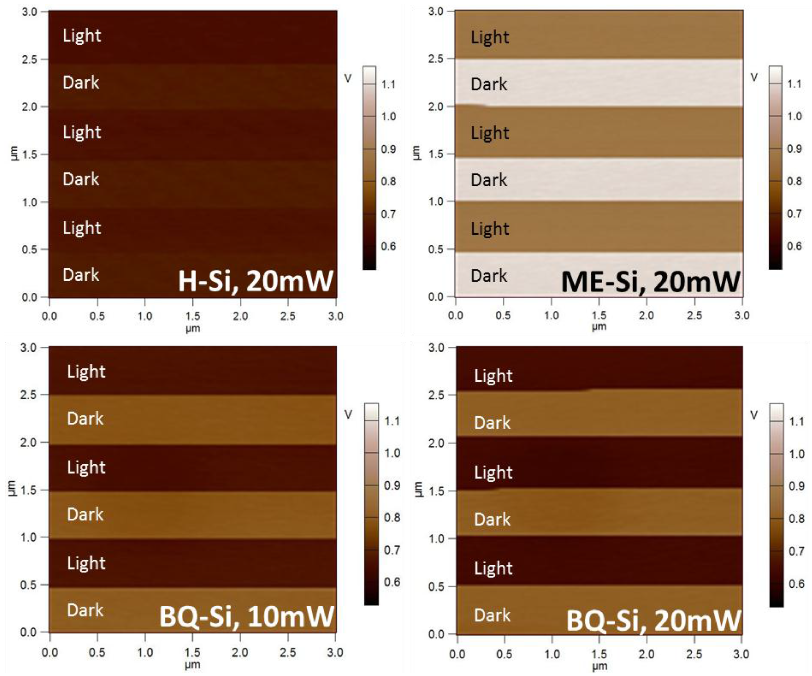
Figure 6.
The (a) contact potential difference (CPD) and (b) surface photovoltage (SPV) measured by Kelvin probe for n-type silicon wafers under three surface treatments—H-Si, BQ-Si, and ME-Si—with respect to HOPG. A reproducible shift of CPD is observed when the 650 nm light was switched on and off during scan.

Figure 7.
Energy levels measured in a dark Kelvin probe measurement (a) and light Kelvin probe measurement in the flat-band condition (b).
Figure 7.
Energy levels measured in a dark Kelvin probe measurement (a) and light Kelvin probe measurement in the flat-band condition (b).

Figure 8.
Cross-section of a unit cell and the corresponding laterally averaged electrostatic potential profile for the H-Si (a) and BQ-Si (b) slab. The potential difference between the Fermi level and the vacuum is denoted.
Figure 8.
Cross-section of a unit cell and the corresponding laterally averaged electrostatic potential profile for the H-Si (a) and BQ-Si (b) slab. The potential difference between the Fermi level and the vacuum is denoted.
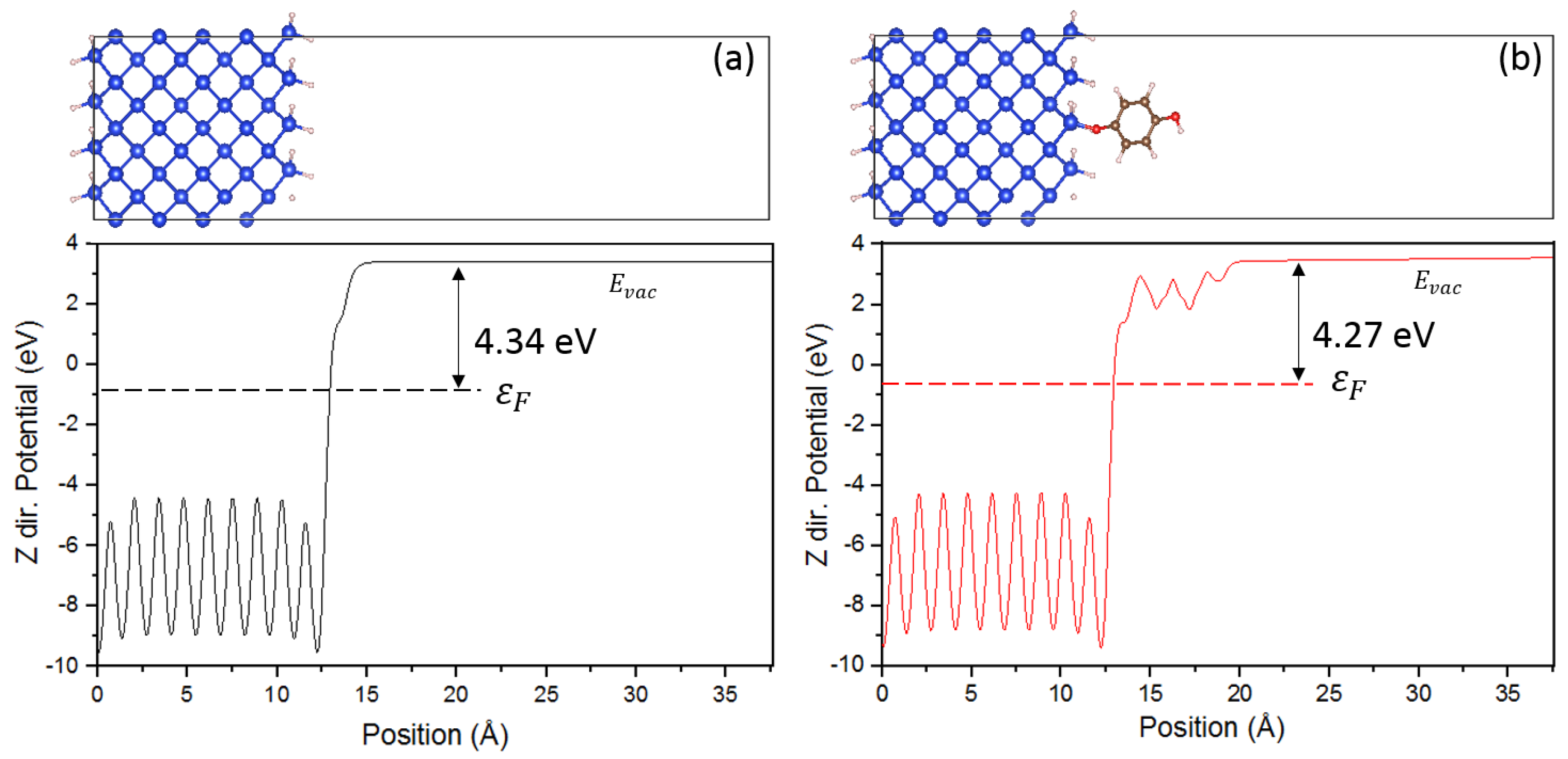
Figure 9.
Electronic structure of BQ passivated n-Si surfaces. Both the negative dipole δ and the downward band bending contribute to the decrease of the Si surface work function upon bonding of BQ radicals.
Figure 9.
Electronic structure of BQ passivated n-Si surfaces. Both the negative dipole δ and the downward band bending contribute to the decrease of the Si surface work function upon bonding of BQ radicals.

© 2018 by the authors. Licensee MDPI, Basel, Switzerland. This article is an open access article distributed under the terms and conditions of the Creative Commons Attribution (CC BY) license (http://creativecommons.org/licenses/by/4.0/).
Share and Cite
MDPI and ACS Style
Chen, M.; Hack, J.H.; Lin, X.; Janotti, A.; Opila, R.L. Electronic Structure Characterization of Hydrogen Terminated n-type Silicon Passivated by Benzoquinone-Methanol Solutions. Coatings 2018, 8, 108. https://doi.org/10.3390/coatings8030108
AMA Style
Chen M, Hack JH, Lin X, Janotti A, Opila RL. Electronic Structure Characterization of Hydrogen Terminated n-type Silicon Passivated by Benzoquinone-Methanol Solutions. Coatings. 2018; 8(3):108. https://doi.org/10.3390/coatings8030108
Chicago/Turabian StyleChen, Meixi, James H. Hack, Xi Lin, Anderson Janotti, and Robert L. Opila. 2018. "Electronic Structure Characterization of Hydrogen Terminated n-type Silicon Passivated by Benzoquinone-Methanol Solutions" Coatings 8, no. 3: 108. https://doi.org/10.3390/coatings8030108
Note that from the first issue of 2016, this journal uses article numbers instead of page numbers. See further details here.