Article

Study on the Properties of 1319 nm Ultra-High Reflector Deposited by Electron Beam Evaporation Assisted by an Energetic RF Ion Source

Key Laboratory of Chemical Lasers, Dalian Institute of Chemical Physics, Chinese Academy of Sciences, Dalian 116023, China
*
Author to whom correspondence should be addressed.
Coatings 2018, 8(2), 74; https://doi.org/10.3390/coatings8020074
Submission received: 24 December 2017 / Revised: 3 February 2018 / Accepted: 6 February 2018 / Published: 14 February 2018
(This article belongs to the Special Issue Applications of Optical Thin Film Coatings)

Abstract

:
Ultra-high reflectors, working as a critical optical component, has been widely applied as a cavity mirror in fine optical systems such as laser gyro, F-P interferometer, etc. For decades, ion beam sputtering (IBS) technology, which can deposit ultra-low loss and dense layers, has been commonly believed to be the only and irreplaceable method to fabricate ultra-high reflectors. Thus, reports on other methods are rare and a reflectivity above 99.99% obtained by evaporation technology (including ion assisted evaporation) has not been seen yet. In the present study, an energetic radio frequency (RF) ion source was introduced during the electron beam evaporation process, which improved the layer quality dramatically. An ultra-high reflector at 1319 nm with reflectivity of 99.992% (measured by cavity-ring down method) was successfully deposited on a φ100 mm × 25 mm single crystal silicon substrate whose surface roughness was approximately 0.420 nm. The surface figure of the reflector was accurately controlled superior to 1/6λ (λ = 632.8 nm). The measured absorption was approximately 3–5 ppm and the calculated scatter based on surface roughness measurement was approximately 6.64 ppm. Total loss of the reflector was systematically discussed. This study showed that it is possible to apply electron beam evaporation in ultra-high reflector manufacture and the method is capable of depositing reflectors with an aperture larger than φ600 mm which is the maximum capacity of current IBS technology.

1. Introduction

Ultra-high reflector, as a critical component, has been widely applied as a cavity mirror in fine optical systems. To meet the demand of laser gyro industry, ion beam sputtering (IBS) was initially developed to fabricate small (<25 mm) and ultra-high reflectors in 1970s [1,2]. Driven by strong demands for ultra-high reflectors for cutting-edge optical technology—such as laser interferometer gravitational-wave observatory (LIGO), ring laser gyro (RLG), high-precision laser resonator [3,4,5,6], etc.—a lot of research has been carried out on IBS technology ranging from device improvement to deposition process. High reflectors fabricated by IBS can reach total losses below 1 ppm [7] and a reflectivity of 99.99984% [8]. For decades, IBS technology has been commonly believed to be the only and irreplaceable method to fabricate ultra-high reflectors. Thus, reports on other methods are rare and a reflectivity above 99.99% obtained by evaporation technology (including ion assisted evaporation) has not been seen yet. Due to the extraordinary properties, the IBS technique has also been tried to fabricate supermirrors with large aperture such as VIRGO mirrors [9]. However, the current IBS technique cannot handle substrates above φ600 mm due to limitations of ion source technology to the best of our knowledge.
Electron beam evaporation has always been the most popular method for optical film deposition. Typical application in the frontier of optical technology is the inertial confinement fusion (ICF) laser optics, which are large mirrors (>1 m), has significantly reduced loss requirements and a high damage threshold [10]. Great effort has been made for the evaporation process to reduce defects and improve the damage threshold [11]. Although ion assisted evaporation (IAE) has made great progress [12,13] in past decades, it was still considered an unsuitable method to deposit ultra-high reflectors due to the porous layer structure or rougher interface compared with IBS technology [14]. Commonly reported reflectivity achieved by ion assisted evaporation is below 99.9% [15,16].
To explore the possibility of fabricating super mirror with large aperture, the present paper introduced an energetic RF ion source during the electron beam evaporation process to improve the layer quality. A 1319 nm ultra-high reflector (reflectivity >99.99%) was successfully fabricated. The surface figure was controlled accurately and optical loss of the reflector was measured and analyzed.

2. Experiments

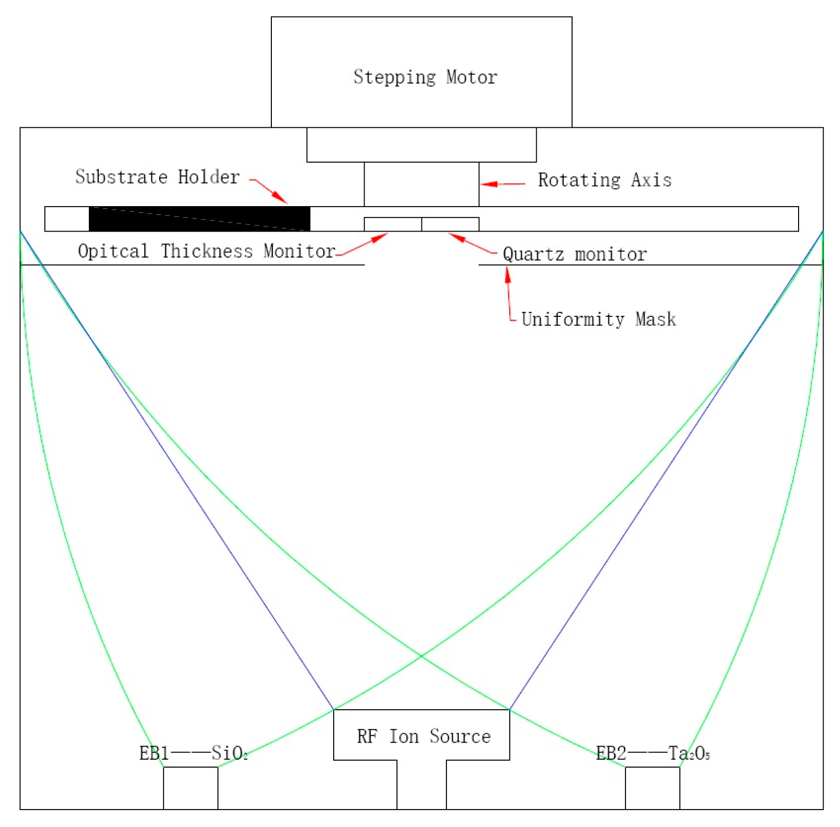
2.1. Sample Preparation

Figure 1 shows the schema of deposition system in present study, which is a traditional electron beam evaporation system (OTFC-1300, Optorun Co., Ltd., Kawagoe-shi, Japan), equipped with a three-Mo-grids RF ion source. The substrate, facing downward, was mounted on a spinning planetary holder. An optical thickness monitor and quartz thickness monitor were deployed in the center of the chamber to control the thickness and deposition rate, respectively. Electron beam evaporation sources and an RF ion source were deployed in the bottom of the chamber. Uniformity masks were used below the substrate holder to adjust the layer thickness distribution across the deposition area. After using the mask, uniformity was superior to ±0.1%.
The layer design of ultra-high reflector was S|(HL)17 H|A, where H denoted high index material (Ta2O5 in present study) with one QWOT (quarter wavelength optical thickness) and L denoted low index material (SiO2 in present study) with one QWOT. S denoted substrate and A denoted the incidence medium (air). The theoretical normal-incidence reflectivity of the design is 99.99961% and the total loss is 3.9 ppm, which was calculated by the well-known Matrix method [17]. In the present study, the refractive index was 2.142 and 1.452 for Ta2O5 and SiO2, respectively.
A single crystal silicon substrate with diameter 100 mm and thickness 25 mm was chosen. The RF ion beam parameters of IAE process were set as: beam voltage = 1100 and 900 V for Ta2O5 and SiO2, respectively; beam current density = 67.8 μA/cm2 for both materials. Compared with traditional ion assisted evaporation, the ion energy is much higher in the present study. O2 was used as the working gas of the ion source, which can also adjust the stoichiometry of the layers. The depositing pressure, which was accurately controlled by an auto pressure control system (APC), was set to 1.63 × 10⁻² Pa for Ta2O5 and 1.45 × 10⁻² Pa for SiO2. The purity of all the working gas was above 99.999%. The deposition rate for Ta2O5 is 0.3 nm/s, while 0.6 nm/s for SiO2.

2.2. Property Measurements

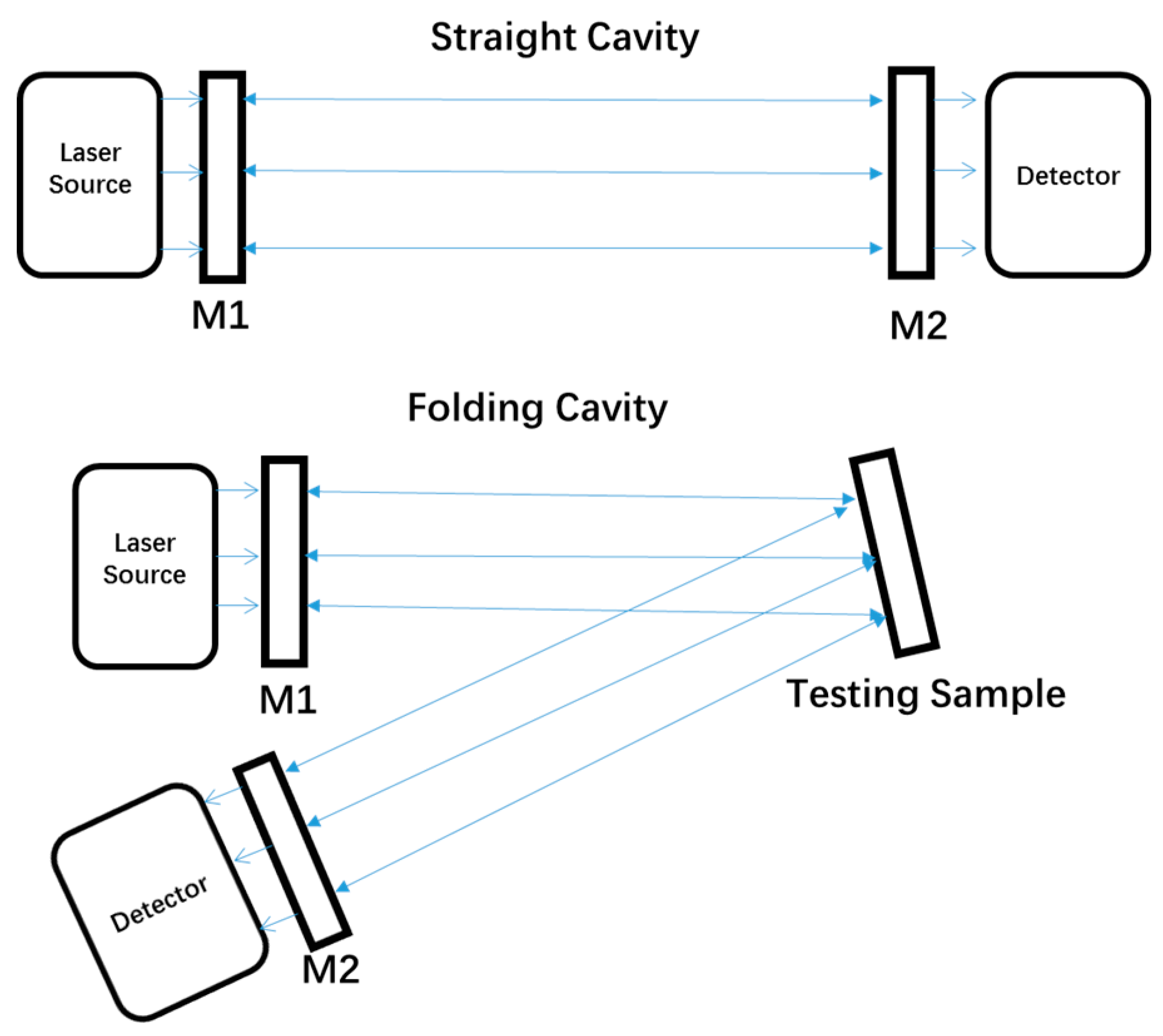
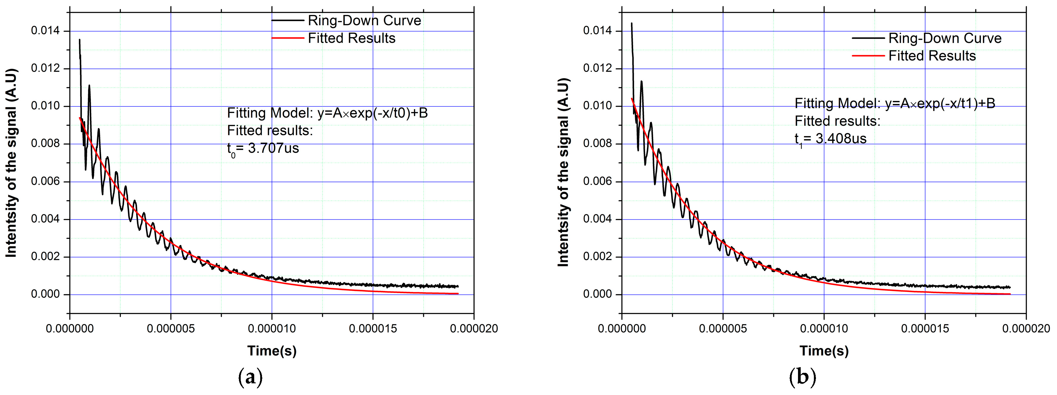
2.2.1. Measurement of Ultra-High Reflectivity

Cavity ring-down method is the only and well-known way to measure ultra-high reflectivity. The basic principles and detailed description of the method have been already reported in literature [18,19]. The present study used cavity ring-down spectroscopy at 1319 nm to measure the ultra-reflectivity. Figure 2 gave the schema of the test platform. The incidence angle is 5°. The reflectivity can be calculated by the formula:
R = e [ L C × ( 1 t 0 1 t 1 ) ]
where L is the length of the cavity (1 m in our study) and C is the velocity of light. t0 and t1 the decay time of the ring-down signal in the straight cavity and folding cavity, respectively, which can be obtained by fitting the ring-down signal to the equation:
y = A × exp ( x t ) + B
where t is the decay time.

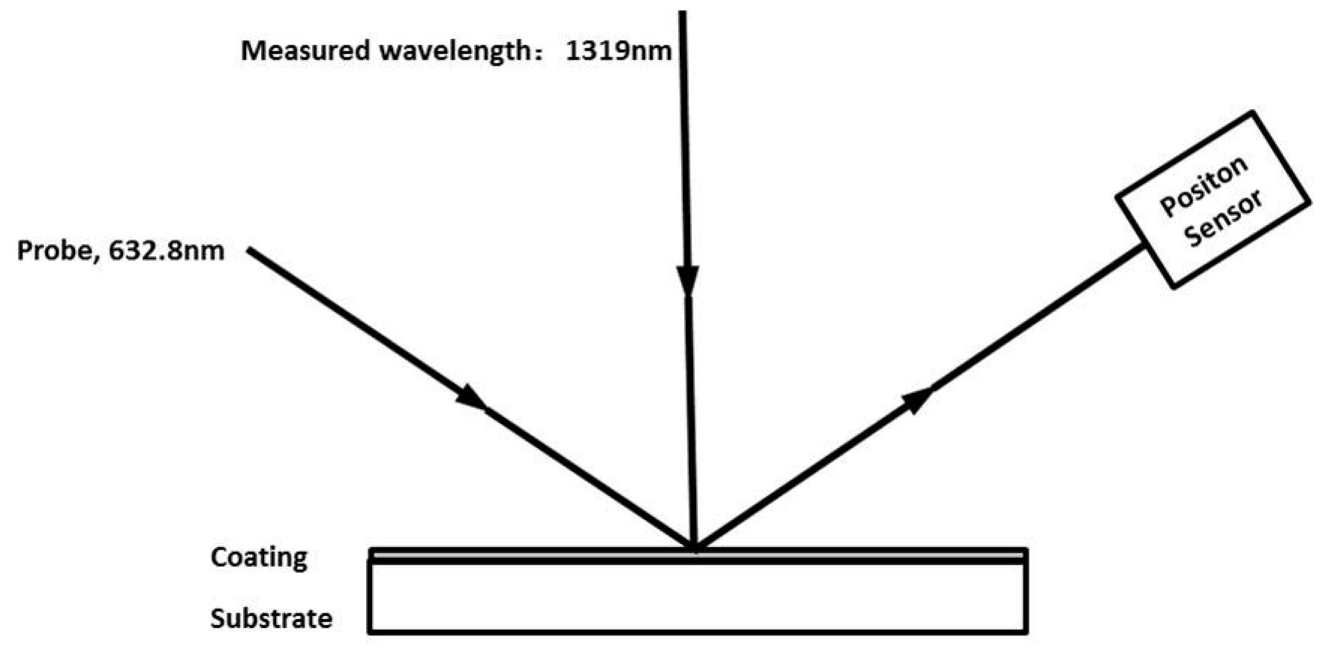
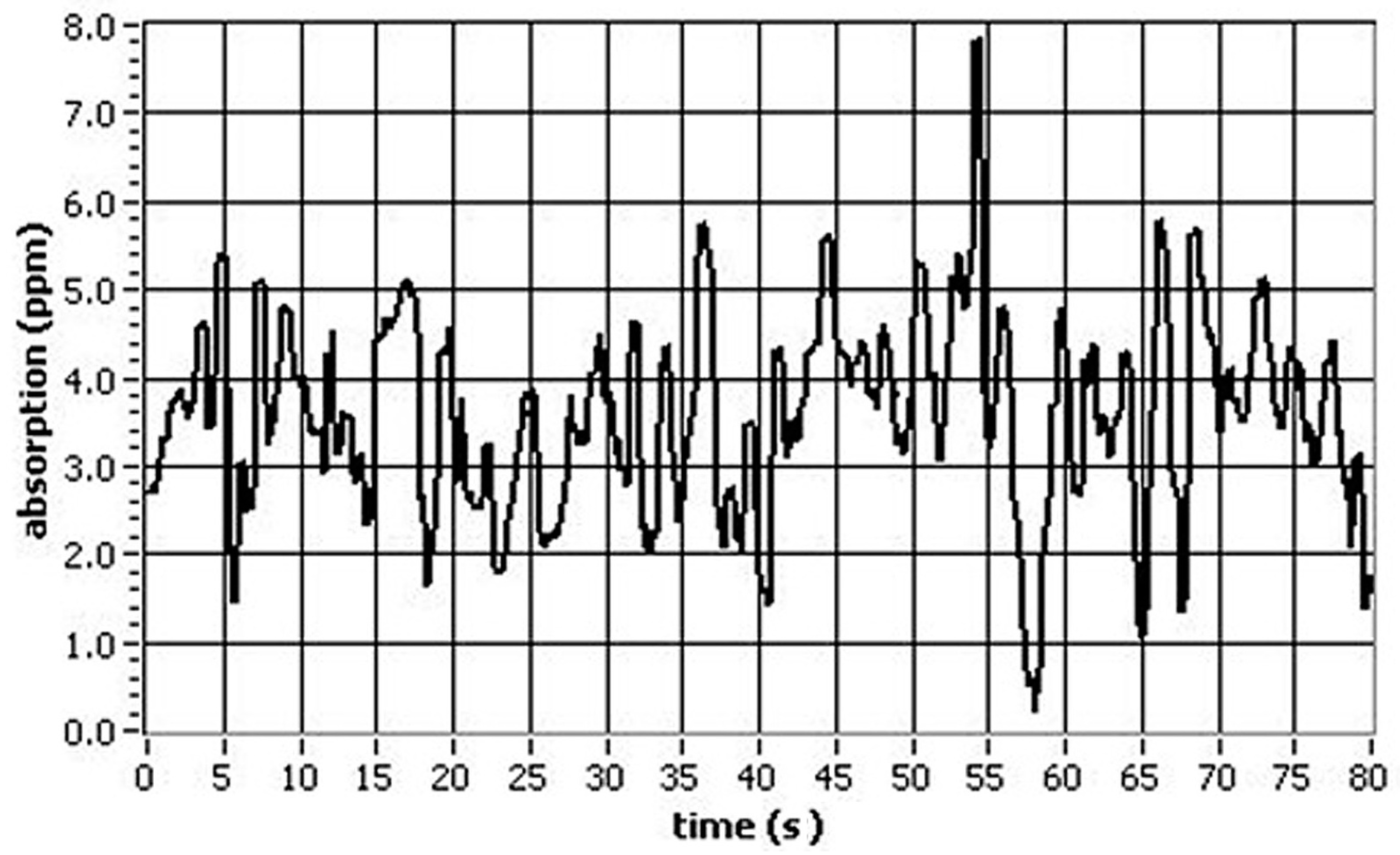
2.2.2. Optical Absorption Measurement

Optical absorption was measured by surface thermal lensing (STL) method [20]. STL is based on creation of phase mismatch between the central and annular portions of the probe beam (632.8 nm, continuous wave (CW)) which is due to the thermal-optic effect caused by the heat deposit by pump beam (1319 nm). Figure 3 gives the schema of the measurement setup. Since the self-interference inside the probe beam, a localized perturbation at the chopping frequency occurs at the center of the Gaussian profile at one Rayleigh length. The non-perturbed annulus of the probe beam is stripped off with an iris and the perturbed components then detected by the position sensor. The wave front phase difference of the perturbed beam can be measured, from which the absorption can be deduced. The platform was calibrated by using a standard sample, which had absorption of 23% at 1319 nm. Counting on this platform, absorptions as low as 0.1 ppm could be detected and measured.

2.2.3. Other Measurement

Roughness (RMS) was determined in by AFM (Atomic Force Microscope, D3100, Veeco, Plainview, NY, USA). Each sample was scanned in 10 different areas with size of 10 μm × 10 μm and the sample’s roughness was determined by the mean value. All the roughness determinations, including substrate and high reflector samples, were carried out in this procedure. The surface figure was measured by interferometer (GPI-XP, Zygo Corporation, Middlefield, CT, USA).

3. Results and Discussion

3.1. Optical Loss Analysis and Reflectivity

Figure 4 gives the surface profile before and after the reflector deposition measured by AFM. It can be seen that surface roughness decreased from 0.420 to 0.323 nm after the layer deposition. The coating process exhibited a planarization effect, which was also observed in the IBS deposition coating process [15], while never being reported in the evaporation coating process. This planarization effect can be explained by the classic thin film growth dynamics: if deposited atoms do not have enough energy to migrate on the surface of substrates, the films would have porous microstructure and rough surface. On the contrary, energetic deposited atoms are capable of migrating long distance on the surface of substrates and stop at proper location with lowest surface energy. The films would possess dense microstructure and smoother surface. Present study used the energetic RF ion source to overcome the shortage of low energy electron beam evaporation. Thus, the deposition atoms can obtain enough energy by momentum transfer with the energetic ions.
The scattering of the ultra-high reflector can be analyzed from the surface roughness. Particular roughness with spatial frequencies range from the wavelength of light to the spot size is the direct contributor to scattering. The correlation between roughness and optical scattering is described in the equation [21].
T I S = 32 π 2 n 0 n H ( n H n L n H + n L ) ( σ λ ) 2
where TIS is total integrated scattering, σ is surface roughness, and λ is working wavelength. n0, nH, and nL are refractive index of incidence media, Ta2O5, and SiO2, respectively. Based on this equation, the total scatter of our ultra-high reflector should be 6.64 ppm.
Figure 5 gives the results of absorption measurement. The measured absorption is approximately 3–5 ppm. This absorption level was much higher than the reported results obtained by IBS and traditional electron beam evaporation [22]. The reason was probably due to the impurities introduced by the energetic ion bombardment [23]. This result was also in accordance with reported conclusions of traditional ion-assisted deposition.
Figure 6a,b shows decay curve of ring-down signals of the straight cavity and folding cavity, respectively. The obtained reflectivity was 99.992%, which is the highest reported reflectivity achieved by electron beam evaporation. According to the measured reflectivity, the total loss of our ultra-high reflectivity is 80 ppm. However, the total loss (scatter and absorption) based on absorption measurement and scatter calculation should be below 11.64 ppm, which is much lower than actual loss. The reasons of this phenomenon are probably due to the scatter: (1) the interface of multilayer was rougher than surface according to the planarization effect discussed above; (2) scattering did not only happen in the interface, but also in the layer due to defects of layer microstructure, which was ignored in above analysis. Thus, the actual value of scatter would be much larger than 6.64 ppm. Limited by our experiment condition, the scattering cannot be directly measured. Compared with the surface roughness of substrate applied in ring laser gyroscopes (below 0.1 nm), the substrate used in the present study was much rougher. Thus, it can be predicted that our reflectivity would be much higher if ultra-smoothing substrate was available for us.

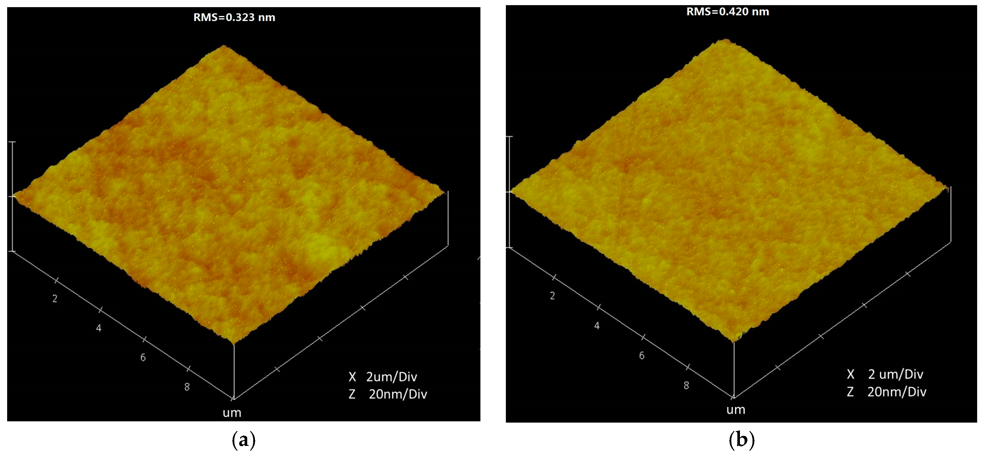
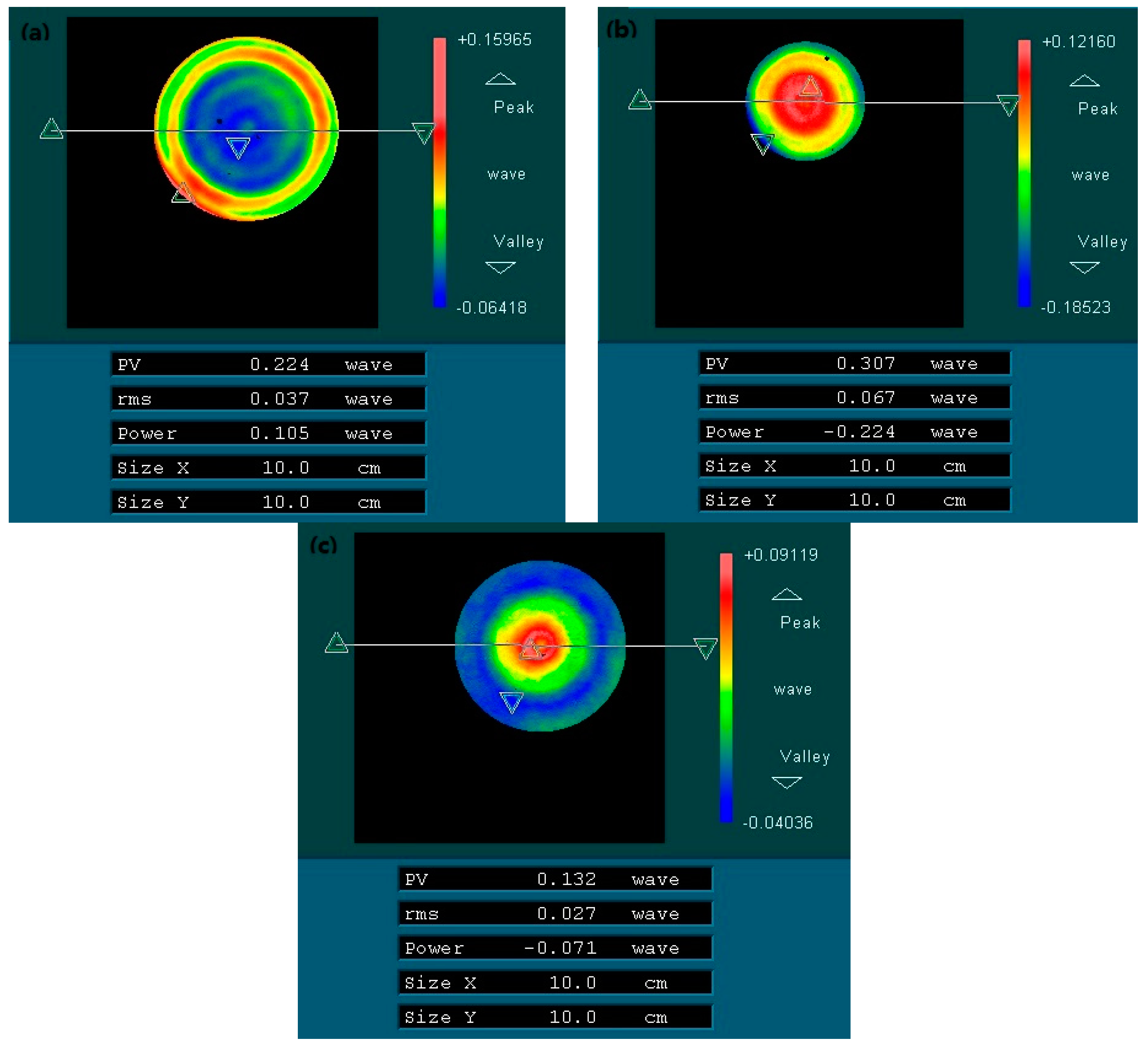
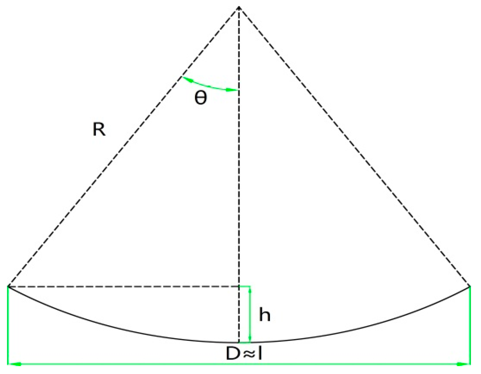
3.2. Surface Figure Control

Surface figure is the deviation between the theoretical and actual profile of the optical surface, which directly influences the wave front of transmission. The surface figure of the reflector can be modified by the residual stress introduced by the coating deposition.
In the present study, the residual stress was calculated based on the Stoney Equation [24]:
σ = E s d s 2 6 ( 1 γ s ) d f ( 1 R 1 1 R 2 )
σ is the residual stress of the coating. Es and γs is the elastic modulus and Poisson ratio of the substrate, respectively. df is the thickness of the film. R1 and R2 are the radius of curvature before and after the coating. ds is the thickness of substrate. Figure 7 shows the schema of substrate surface. D is the diameter of the substrate. Since the θ is small enough due to the flat surface. The following equation can be deduced from the geometry:
D l = 2 R θ
P V = h = R ( 1 cos θ ) = 2 R sin 2 ( θ 2 ) D 2 8 R
The power value change (∆PV) which can be measured by ZYGO interferometer meets the equation:
P V = P V 1 P V 2 = D 2 8 ( 1 R 1 1 R 2 )
Thus, the Stoney equation can be written as:
σ = 4 E s d s 2 3 ( 1 γ s ) D 2 P V d f
For single crystal silicon substrate, Es = 130 GPa and γs = 0.23 were used in the calculation. The diameter of the substrate is 100 mm while the thickness is 25 mm. For our study, df = 6477 nm. ∆PV is the power value change which can be measured by ZYGO interferometer in the present study.
Figure 8a,b showed the surface figure of the substrates and post-deposited ultra-high reflector, respectively. The power value of the surface changed from 0.105λ to −0.224λ (λ = 632.8 nm). The multilayer exhibited compressive stress and the value is 452 MPa, which was fairly high. To compensate the surface figure change, SiO2 single layer were deposited on the backside of the reflector and the surface figure was controlled superior to 1/6λ (λ = 632.8 nm). Figure 8c was the final surface figure of the ultra-high reflector.

4. Conclusions

An ultra-high reflector at 1319 nm with a reflectivity of 99.992% was successfully deposited on single crystal silicon substrate by electron beam evaporation assisted by an energetic RF ion source. To our best knowledge, this was the highest reflectivity obtained by the ion-assisted evaporation technology. The absorption of the reflector was below 5 ppm and the main loss was from the scatter. It can be predicted that higher reflectivity can be obtained if a smoother substrate is used, which we will try in our future work. Backside coating was deposited to control the surface figure of the reflector and high accuracy can be achieved. The present study showed that it is possible to apply electron beam evaporation in ultra-high reflector manufacture and the method is capable of depositing reflectors with aperture larger than φ600 mm which is the maximum capacity of current IBS technology limited by our knowledge.

Author Contributions

Songwen Deng did the literature search, conceived the study design, interpreted the data, and wrote the manuscript. Gang Li participated the study design and data interpretation. Feng Wang and Qipeng Lv collected and analyzed the data. Long Sun and Yuqi Jin participated the study design.

Conflicts of Interest

The authors declare no conflict of interest.

References

  1. Kaufman, H.R. Technology of ion beam sources used in sputtering. J. Vac. Sci. Technol. 1978, 15, 272–276. [Google Scholar] [CrossRef]
  2. Lalezari, R. Low loss ion beam sputtered optical coating and their applications. In Laser-Induced Damage in Optical Materials: 2011, Proceedings of SPIE Laser Damage, Boulder, CO, USA, 18–21 September 2011; Exarhos, G.J., Gruzdev, V.E., Menapace, J.A., Ristau, D., Soileau, M.J., Eds.; SPIE: Bellingham, WA, USA, 2011; p. 819003. [Google Scholar]
  3. Aronowitz, F.; Collins, R.J. Lock-in and intensity-phase interaction in the ring laser. J. Appl. Phys. 1970, 41, 130–141. [Google Scholar] [CrossRef]
  4. Abramovici, A.; Althouse, W.E.; Drever, R.W.; Gursel, Y.; Kawamura, S. LIGO, the laser interferometer gravitational-wave observatory. Science 1992, 256, 325–333. [Google Scholar] [CrossRef] [PubMed]
  5. Gillespie, A.; Rab, F. Thermally excited vibrations of the mirrors of laser in terferometer gravitational-wave detectors. Phys. Rev. D 1995, 52, 577–585. [Google Scholar] [CrossRef]
  6. Thompson, R.J.; Rampe, G.; Kimble, H.J. Observation of normal-mode splitting for an atom in an optical cavity. Phys. Rev. Lett. 1992, 68, 1132–1135. [Google Scholar] [CrossRef] [PubMed]
  7. Jolly, T.W.; Lalezari, R. Ion beam sputter deposition techniques for the production of optical coating of the highest quality. In Thin Films for Optical Systems, Proceedings of Optical Systems Design ’92, Berlin, Germany, 1–30 September 1992; Guenther, K.H., Ed.; SPIE: Bellingham, WA, USA, 1993; pp. 250–255. [Google Scholar]
  8. Rempe, G.; Thonpson, R.J.; Kimble, H.J. Measurement of ultra-low losses in an optical interferometer. Opt. Lett. 1992, 17, 363–365. [Google Scholar] [CrossRef] [PubMed]
  9. Forest, D.; Ganau, P.; Lagrange, B.; Mackowski, J.M.; Michel, C.; Montorio, J.L.; Morgado, N.; Pignard, R.; Pinard, L.; Remillieux, A. coatings on large substrates: Towards an improvement of the mechanical and optical performances. Appl. Opt. 2006, 45, 1436–1438. [Google Scholar]
  10. Christopher, J.; Francois, Y.S.; Mark, R.G. Influence of microstructure on laser damage threshold of IBS coatings. In 27th Annual Boulder Damage Symposium: Laser-Induced Damage in Optical Materials: 1995, Proceedings of Laser-Induced Damage in Optical Materials: 1995, Boulder, CO, USA, 30 October–1 November 1995; Bennett, H.E., Guenther, A.H., Kozlowski, M.R., Newnam, B.E., Soileau, M.J., Eds.; SPIE: Bellingham, WA, USA, 1996; pp. 351–360. [Google Scholar]
  11. Sheehana, L.M.; von Gunten, M.K.; Bevis, R.P.; Smith, D.J. The advantages of evaporation of Hafnium in a reactive environment to manufacture high damage threshold multilayer coating by electron-beam deposition. In Advances in Optical Interference Coatings, Proceedings of Optical Systems Design and Production, Berlin, Germany, 26–29 May 1999; Amra, C., Macleod, H.A., Eds.; SPIE: Bellingham, WA, USA, 1999; pp. 318–324. [Google Scholar]
  12. Ehlers, H.; Lappshies, M.; Ristau, D. Ion assisted deposition processes for precision and laser optics. In Advances in Optical Thin Films, Proceedings of Optical Systems Design, St. Etienne, France, 30 September–3 October 2003; Amra, C., Kaiser, N., Macleod, H.A., Eds.; SPIE: Bellingham, WA, USA, 2004; pp. 519–528. [Google Scholar]
  13. Ehlers, H.; Becker, K.; Beckmann, R.; Beermann, N.; Brauneck, U.; Fuhrberg, P.; Gaebler, D.; Jakobs, S.; Kaiser, N.; Kennedy, M.; et al. Ion Assisted Deposition Processes: Industrial Network IntIon. In Advances in Optical Thin Films, Proceedings of Optical Systems Design, St. Etienne, France, 30 September–3 October 2003; Amra, C., Kaiser, N., Macleod, H.A., Eds.; SPIE: Bellingham, WA, USA, 2004; pp. 646–656. [Google Scholar]
  14. Cho, H.-J.; Shin, M.-J.; Lee, J.-C. Effects of substrate and deposition method onto the mirror scattering. Appl. Opt. 2006, 45, 1440–1446. [Google Scholar] [CrossRef] [PubMed]
  15. Stolz, C.J.; Wolfe, J.E.; Mirkarimi, P.B.; Folta, J.A.; Adams, J.J.; Menor, M.G.; Teslich, N.E.; Soufli, R.; Menoni, C.S.; Patel, D. Defect insensitive 100 J/cm2 multilayer mirror coating process. In Laser-Induced Damage in Optical Materials: 2013, Proceedings of SPIE Laser Damage, Boulder, CO, USA, 23–26 September 2013; Ristau, D., Ed.; SPIE: Bellingham, WA, USA, 2013; p. 888502. [Google Scholar]
  16. Ai, W.; Xiong, S. Investigation of laser-induced damage threshold of hafnia/silica high reflectors at 1064 nm. In Pacific Rim Laser Damage 2011: Optical Materials for High Power Lasers, Proceedings of Pacific Rim Laser Damage Symposium: Optical Materials for High Power Lasers, Shanghai, China, 6–9 November 2011; Shao, J., Ed.; SPIE: Bellingham, WA, USA, 2012; p. 82060G. [Google Scholar]
  17. Macleod, H.A. Basic theory. In Thin-Film Optical Filters; Institute of Physics Publishing: London, UK, 2010; pp. 40–42. [Google Scholar]
  18. Dana, Z.; Anderson, J.C.; Carl, S.M. Mirror reflectometer based on optical cavity decay time. Appl. Opt. 1984, 23, 1238–1245. [Google Scholar]
  19. Virgil, S. High-precision reflectivity measurement technique for low-loss laser mirrors. Appl. Opt. 1977, 16, 1238–1245. [Google Scholar]
  20. Boccara, A.C.; Fournier, D.; Badoz, J. Thermo-optical spectroscopy: Detection by the “mirage effect”. Appl. Phys. Lett. 1980, 36, 130–132. [Google Scholar] [CrossRef]
  21. Macleod, H.A. Multilayer high-reflectance coatings. In Thin-Film Optical Filters; Institute of Physics Publishing: London, UK, 2010; pp. 204–208. [Google Scholar]
  22. Stolz, C.J.; Taylor, J.R. Damage threshold study of ion beam sputtered coating for a visible high-repetition laser at LLNL. In 24th Annual Boulder Damage Symposium Proceedings—Laser-Induced Damage in Optical Materials: 1992, Proceedings of Optical Materials For High Power Lasers, Boulder, CO, USA, 28–30 September 1992; Bennett, H.E., Chase, L.L., Guenther, A.H., Newnam, B.E., Soileau, M.J., Eds.; SPIE: Bellingham, WA, USA, 1992; pp. 182–190. [Google Scholar]
  23. Pearson, D.I.; Pochon, S.; Cooke, M. Pearson, Sebastien Pochon, Mike Cooke. Contamination control in ion beam sputter-deposited films. In Nanoengineering: Fabrication, Properties, Optics, and Devices X, Proceedings of SPIE NanoScience + Engineering, San Diego, CA, USA, 25–29 August 2013; Campo, E.M., Dobisz, E.A., Eldada, L.A., Eds.; SPIE: Bellingham, WA, USA, 2004; p. 88161K. [Google Scholar]
  24. Yoon, S.G.; Kim, Y.T.; Kim, H.K. Comparison of residual stress and optical properties in Ta2O5 thin films deposited by single and dual ion beam puttering. Mater. Sci. Eng. B 2005, 118, 234–237. [Google Scholar] [CrossRef]
Figure 1. Schema of deposition system.
Coatings 08 00074 g001
Figure 2. Schema of cavity ring-down spectroscopy.
Coatings 08 00074 g002
Figure 3. Schema of the low absorption measurement.
Coatings 08 00074 g003
Figure 4. Surface profile measured by AFM: (a) ultra-high reflector; (b) single crystal silicon substrate.
Coatings 08 00074 g004
Figure 5. Absorption of the ultra-high reflector.
Coatings 08 00074 g005
Figure 6. Decay curve of ring-down signal: (a) straight cavity; (b) folding cavity.
Coatings 08 00074 g006
Figure 7. Schema of substrate surface.
Coatings 08 00074 g007
Figure 8. Surface figure measurement: (a) substrate; (b) post-deposited; (c) backside coating compensation.
Coatings 08 00074 g008

