
Photovoltaic Effect in Graphene/MoS2/Si Van der Waals Heterostructures

Suzhou University of Science and Technology, Suzhou 215011, China
*
Author to whom correspondence should be addressed.
Coatings 2018, 8(1), 2; https://doi.org/10.3390/coatings8010002
Submission received: 16 October 2017
/
Revised: 7 December 2017
/
Accepted: 19 December 2017
/
Published: 21 December 2017
(This article belongs to the Special Issue Graphene and Other 2D Layered Nanomaterial-Based Films: Synthesis, Properties and Applications)
Abstract
:This paper presents a study on the photovoltaic effect of a graphene/MoS2/Si double heterostructure, grown by rapid chemical vapor deposition. It was found that the double junctions of the graphene/MoS2 Schottky junction and the MoS2/Si heterostructure played important roles in enhancing the device’s performance. They allowed more electron-hole pairs to be efficiently generated, separated, and collected in the graphene/MoS2/Si double interface. The device demonstrated an open circuit voltage of 0.51 V and an energy conversion efficiency of 2.58% under an optical illumination of 500 mW/cm2. The photovoltaic effect of the device was partly attributed to the strong light absorption and photoresponse of the few-layer MoS2 film, and partly ascribed to the high carrier-collection-rate of the double van der Waals heterostructures (vdWHs) in the device.
1. Introduction
Recently, van der Waals heterostructures (vdWHs), consisting of various two-dimensional (2D) materials such as graphene, transition metal sulfide (MoS2, WSe2, etc.) and boron nitride (h-BN), have given rise to many interesting results and phenomena [1,2,3]. Not only have horizontal and vertical vdWHs increased our physical understanding of 2D systems, but can also be used to fabricate various novel 2D devices, such as vertical transistors, field effect transistors, photodetectors, and photoresponsive memory devices [4,5,6]. In particular, the graphene/MoS2 heterostructure has emerged as a potential candidate for various novel optoelectronic devices because of the excellent optical properties of MoS2, the high transparency of graphene, and the tunability of its Fermi level [7,8,9]. Despite the many advantages of the 2D-vdWHs, it was found that the photoelectric conversion efficiency of such optoelectronic devices is no higher than that of the bulk devices. For example, Furchi et al. and Gong et al. reported a conversion efficiency of approximately 0.2% [10] and 0.1% [11] with the MoS2/WSe2 and WSe2/MoSe2 heterostructures, respectively. 2D devices also exhibit a pronounced response to optical signals. This is because, although the 2D materials have good photoresponse characteristics, their weak photoelectron collection ability leads to a high recombination rate and low conversion efficiency. Therefore, it is necessary to further enhance the collection rate of the photogenerated carriers, thereby increasing the photoelectric conversion efficiency. In this work, we designed a graphene/MoS2/Si double heterostructure, that is, the graphene/MoS2 Schottky junction and the MoS2/Si heterostructure. These were used to improve the collection rate of photogenerated carriers, as well as the photoelectric conversion efficiency. The graphene/MoS2/Si double vdWHs were prepared by a rapid chemical vapor deposition, and the photovoltaic effect was investigated. A small Schottky barrier was formed between the few-layer graphene and MoS2 layer due to the difference in their work function, and a large pn barrier was formed between MoS2 and Si substrate, which accelerated the separation of the photogenerated electron–hole pairs and enhanced the carrier collection capability, thus providing a better optical and electrical performance.
2. Materials and Experiment
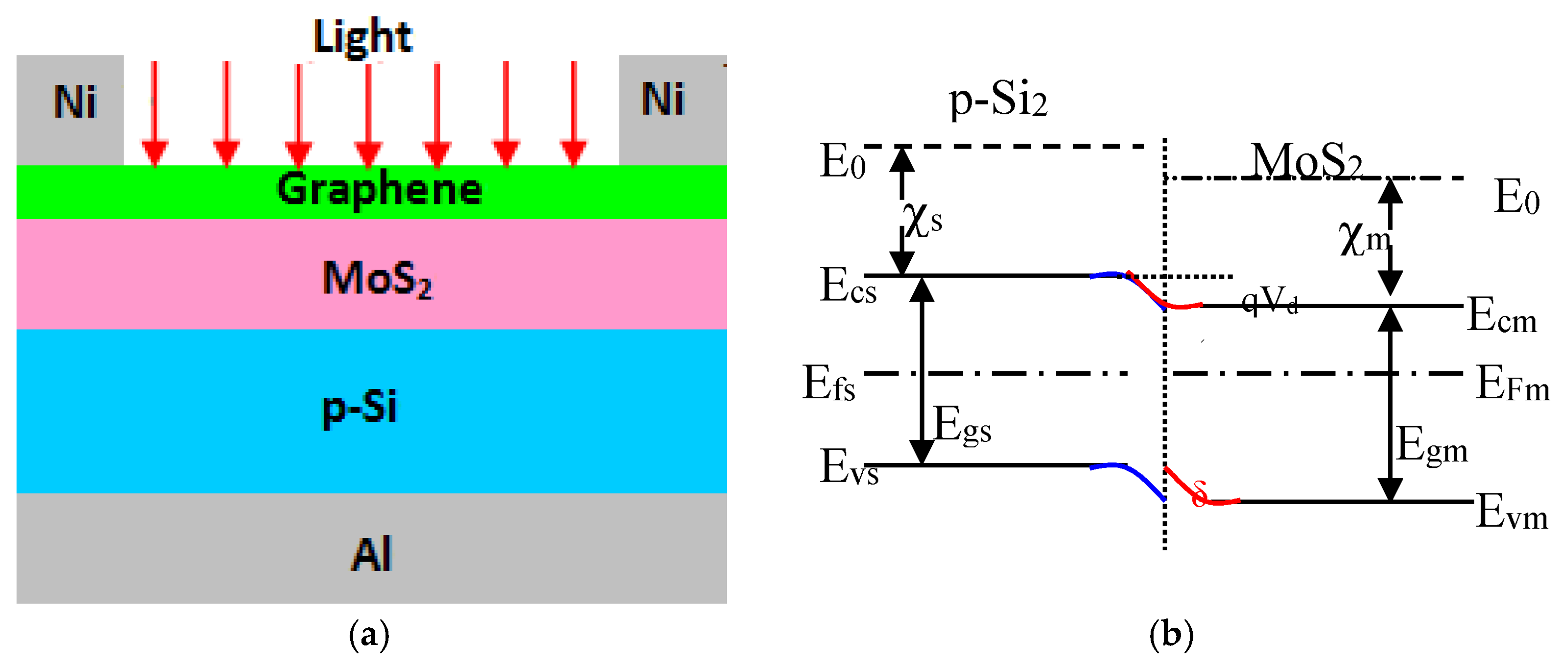
The structure of the studied graphene/MoS2/p-Si vdWHs was composed of a graphene layer, a MoS2 layers, a p-Si, and Ni, Al electrodes; the schematic and the energy band diagram is shown in Figure 1a,b. In Figure 1b, Ecs, Evs, EFs, and χs are the conduction band, valence band, Fermi level, and electron affinity, respectively, of Si, while Ecm, Evm, EFm, and χm are the conduction band, valance band, Feimi level and electron affinity, respectively, of MoS2. For Si, χs = 4.0 eV, Egs = 1.12 eV. For MoS2, χm = 4.05 eV, Egs = 1.4 eV [12]. E0 is the vacuum level, and qV is the built-in potential between p-Si and MoS2. The graphene and MoS2 layers were fabricated on a p-Si surface by a rapid chemical vapor deposition (CVD) process. The growth system was made up of a large horizontal quartz tube furnace, a vacuum system, a gas meter, and an automatic temperature controller. p-Si (100) substrates with a size of 12 mm × 12 mm × 500 mm were cleaned ultrasonically with a sequence of acetone, ethanol, and deionized water, blown with N2 to dry them, and finally placed at the center of the furnace. Prior to deposition, the furnace was pumped to 10−2 Pa, and heated to 300 °C for 10 min to remove any water moisture. 1 g Analytical grade MoS2 micro powder and 1 g silver nitrate (AgNO3) powder were dissolved in 200 mL of 5% diluted sulfuric acid (H2SO4) by stirring for 5 min at 70 °C in a water bath. Here, H2SO4 is a solvent to dissolve MoS2 powder to become saturated solution, and AgNO3 is a dopant to dope MoS2 film in situ, which can effectively improve the electrical conductivity of MoS2 film [13]. Argon (Ar) gas was passed through the mixed solution at a flow rate of 10 cm3/min to carry AgNO3 and MoS2 into the reaction furnace. Growth was carried out for 5–10 min, followed by in situ annealing at 800 °C for 30 min. Then, a mixture of pure CH4 gas (99.999%) and Ar gas with a volume ratio of 1:10 was introduced into the reactive chamber, where the temperature was kept at 950 °C. CH4 was initially decomposed to give a mixture of C and H2, and the C atoms condensed to form graphene film [14]. The growth process was carried out for 5 min, and then the samples were annealed at 1000 °C for 30 min. Finally, the samples were removed out when the system had cooled down to room temperature, Ni electrodes (2 mm × 2 mm, 300 nm) were formed by a sputtering method through a shadow mask at the corner of the graphene film, and Al electrode were deposited on the backside of the Si substrate.
The morphology and structure of the samples were characterized by atomic force microscopy image (AFM, MultiMode 8, Bruker, Billerica, MA, USA) and Raman spectroscopy (Spex-1403, INC, Metuchen, NJ, USA). The optical transparency profiles of the graphene and MoS2 films were investigated by UV-Vis spectroscopy (UV3600, Shimadzu, Kyoto, Japan). Finally, the photovoltaic characteristics of the graphene/MoS2/p-Si structure were evaluated by a Keithley (Cleveland, OH, USA) 4200 SCS under white light illumination.
3. Result and Discussion
Figure 2a shows an atomic force microscopy (AFM) image of the deposited graphene film. A large uniform graphene film was formed on the substrate, on which some newly generated slices were scattered. From the scale picture in Figure 2b, we can estimate that the thickness of the yellow uniform graphene is approximately 2.5 nm, equaling a few layers of graphene, the highest height of the film is about 5.66 nm. Figure 1c shows the Raman spectrum of the deposited graphene film. We can see that two major scattering peaks appear in the spectrum, a 2D-band peak at 2692 cm−1 and a G-band peak at 1580 cm−1. The intensity ratio of IG:I2D = 2 confirms that this is a few-layer graphene [15].
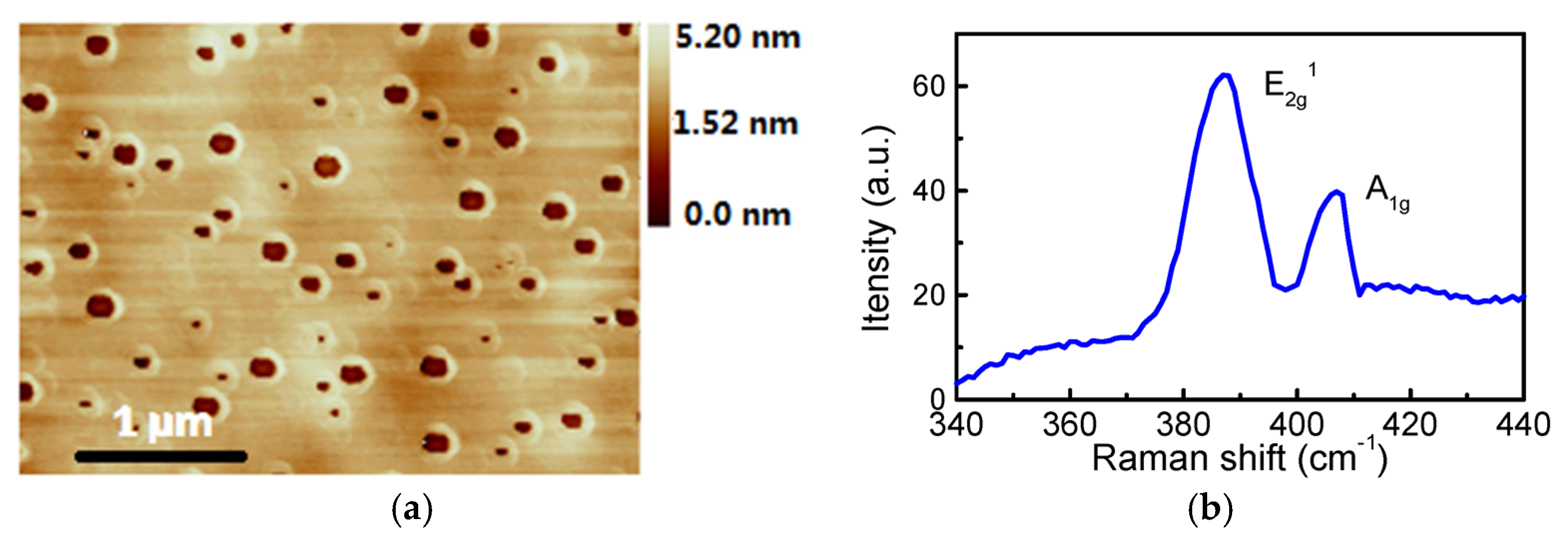
Figure 3a shows the AFM image of MoS2 film deposited on the Si substrate. It is seen that many MoS2 rings with thicknesses of approximately 5 nm are uniformly distributed on the surface, which is equivalent to ten layers of MoS2. The sublayer MoS2 is a homogeneous, continuous film with a thickness of approximately 5 nm. The rings take a circular shape with an inner and outer diameter of 50 and 100 nm respectively. They are uniformly scattered on the substrate without any overlap, dislocation or defect, indicating that they are formed by an excellent self-organized growth process with a layer-by-layer growth mode. Figure 2b shows the Raman spectrum of MoS2 with two typical strong waving peaks at 385 cm−1 and 406 cm−1, corresponding to the in-plane () and the out-of-plane (A1g) modes respectively [16]. It has been reported that the mode is attenuated and the A1g mode is strengthened with increasing layer thickness [16], which is similar to other layered materials, where the bond distance changes with number of layers [17]. The frequency difference of the Raman modes of A1g and is about 21 cm−1, indicating that the deposited MoS2 is few-layered, based on [18,19].
The transmittance of the graphene sample in the visible light range of 400–800 nm is shown in Figure 4a. The optical transparency of the graphene deposited for 5 min was over 80% in the visible range. Moreover, the transparency increases with wavelength, becoming almost fully transparent for the range of 600–800 nm. A high transmittance is very useful for making solar cells, because light in the 400–800 nm range has higher power. Theoretically, the transparency of graphene drops quickly with thickness [20]. However, the actual measured transparency of graphene does not closely obey this pattern. Wang et al. reported that the transparency of GO is over 80% in 550 nm light at a thickness of 22 to 78 nm [21]. Figure 3b shows the UV-Vis absorption spectra of the MoS2/Si heterojunction sample in the wavelength range of 250–900 nm. The absorption peak for the MoS2 film, corresponding to the band gap of MoS2 (approximately 1.69 eV), is located at 735 nm, and the absorption peak of Si occurs at 850 nm. It is clear that the optical absorption of the MoS2/Si heterojunction covered the visible and near-infrared spectral regions of 350–900 nm, which could help to improve the efficiency of solar cells.
Figure 5a,b shows the current-voltage (I–V) characteristic curves of the graphene/MoS2/Si heterojunction solar cell under different light energy densities without and with illumination, respectively. Without illumination, the positive current I increases exponentially with the applied voltage for V > 0, while the reverse current reduces to almost zero when V < 0. The heterojunction shows very low reverse saturation current and rectification properties. This shows that the heterojunction has good interface and contact properties, although there is a large lattice mismatch between MoS2 and graphene. No reconstruction is expected when they contact closely [22], because there are few dangling bonds and surface states in the two dimensional films, and they are compacted by van der Waals interaction with minimum strain. The I–V curves measured with optical power densities from 100 to 500 mW/cm2 are presented in Figure 5b. The reverse current is much higher here than that during darkness, and all the curves in reverse bias show good saturation characteristics. Clearly, the current increases with increasing light energy. The heterojunction has a large open circuit voltage (Voc) of 0.51 V, and a short-circuit current of 0.51 μA at an illumination of 500 mW/cm2.
A Schottky barrier forms between the graphene and MoS2 film, and a pn heterostructure forms between the MoS2 film and Si substrate. Since the graphene layer has high transmission properties, only a small part of the light will be absorbed by the few-layer graphene, while a large part will pass through. The transmitted light is further absorbed by the MoS2 film and Si substrate, which produces intrinsic absorption when the photon energy is larger than the optical band gap, giving rise to photogenerated electron–hole pairs. The holes, being the minority carrier in the MoS2 layer, have a concentration gradient, which will diffuse to the space-charge region boundary of MoS2/Si heterojunction. Thereafter, they are accelerated to the Si side under the built-in electric field in the space-charge region. Thus, the photogenerated electrons and holes are separated by the built-in electric field in the space, and they accumulate on the MoS2 and Si sides, respectively, generating the photovoltaic effect between the MoS2 and Si surface.
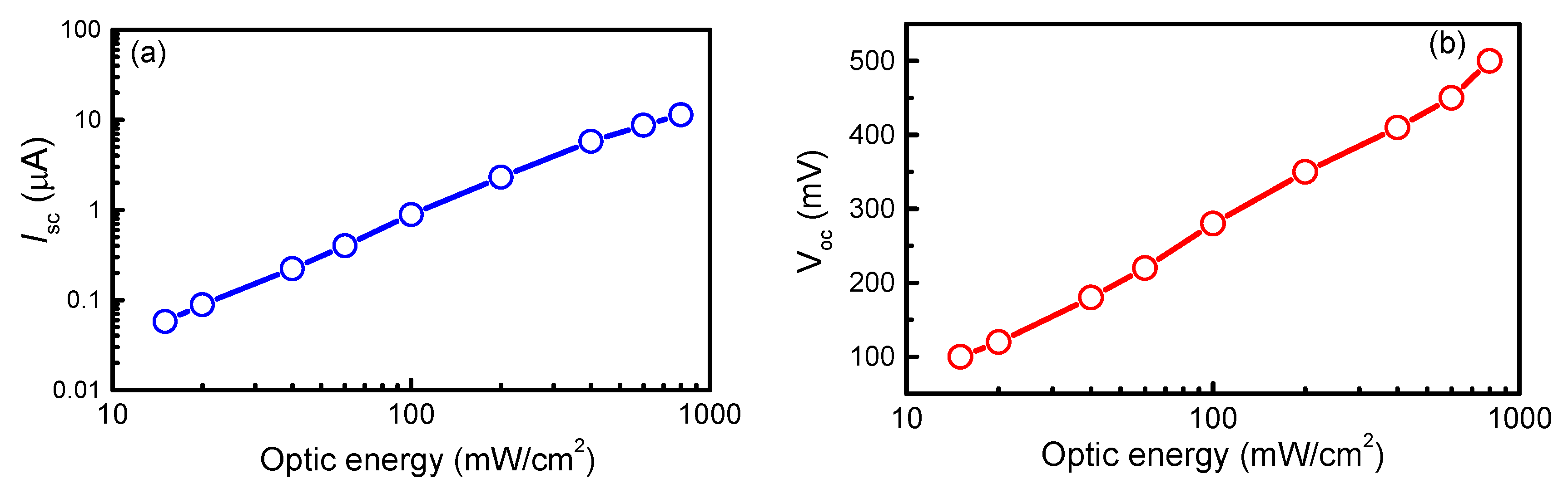
The short-circuit current (ISC) and the open-circuit voltage (VOC) of the graphene/MoS2/Si heterojunction solar cell with different light energies are shown in Figure 6a,b, respectively. VOC represents the voltage when no current is flowing through the device, while ISC shows the current at zero voltage between the electrodes. Generally, ISC and VOC linearly increase with light energy because the photogenerated carriers are in direct proportion to the light energy [23]. We can see that the conversion of optical energy into electrical energy of the graphene/MoS2/Si device is approximately 2.5%. It is larger than the previously reported values of 2.15% and 1.47% for a monolayer graphene film/Si-nanowire-array Schottky junction solar cell [16] and graphene nanoribbon/multiple-silicon-nanowires junctions [24], respectively. Moreover, it is almost ten times larger than that of the MoS2/WSe2 [10] and the WSe2/MoSe2 Heterostructures [11]. The high conversion efficiency in our work may be attributed to the following reason. Firstly, electrons in the graphene layer have high mobility, which imparts good conductivity and low contact resistance. Secondly, the double junctions can accelerate the separation process of the photogenerated electrons and holes, thereby decreasing their recombination. Finally, the bulk Si substrate has high carrier collection capability, which can effectively enhance the conversion efficiency.
From the results, we deposited a large area of uniform graphene and MoS2 films by chemical vapor deposition. The graphene/MoS2/Si heterojunctions have good I–V properties, photovoltaic effect and high photoelectric conversion efficiency, showing that the heterojunction has good contacting and interface properties, which could be used to fabricate high-efficiency solar cells, optical detectors, and other light-response devices.
4. Conclusions
Few-layer graphene and MoS2 films were prepared on a Si substrate by rapid chemical vapor deposition, and the photovoltaic effects of the graphene/MoS2/Si double-junction were investigated. The graphene and MoS2 films have a large-area uniform morphology with a thickness of tens of monolayers. The graphene/MoS2 heterojunction has good interface and photoelectric response properties. An open-circuit voltage of 0.51 V and an energy conversion efficiency of 2.58% were achieved under an illumination energy of 500 mW/cm2. The higher conversion efficiency was attributed to the double junction and Si substrate, which played important roles in collecting carriers and enhancing the conversion efficiency. The double-junction device can harvest solar light and generate more electron–hole pairs efficiently.
Acknowledgments
This work is supported in part by the National Natural Science Foundation of China (No. 31570515) and the Scientific Project Program of Suzhou City (No. SYN201511).
Author Contributions
Weilin Shi contributed with the experimental components regarding tool preparation, sample deposition and measurement; Xiying Ma designed the experiments, analyzed the data and wrote the paper.
Conflicts of Interest
The authors declare no conflict of interest. The founding supporters had no role in the design of the study; in the collection, analyses, or interpretation of data; in the writing of the manuscript, and in the decision to publish the results.
References
- Shih, C.; Wang, Q.H.; Son, Y.; Jin, Z.; Blankschtein, D.; Strano, M.S. Tuning on-off current ratio and field-effect mobility in a MoS2-graphene heterostructurevia Schottky barrier modulation. ACS Nano 2014, 8, 5790–5798. [Google Scholar] [CrossRef] [PubMed]
- Kwak, J.Y.; Hwang, J.; Calderon, B.; Alsalman, H.; Munoz, N.; Schutter, B.; Spencer, M.G. Electrical characteristics of multilayer MoS2 FET’s with MoS2/graphene heterojunction contacts. Nano Lett. 2014, 14, 4511–4516. [Google Scholar] [CrossRef] [PubMed]
- Baugher, B.W.H.; Churchill, H.O.H.; Yang, Y.; Jarillo-herrero, P. Optoelectronic devices based on electrically tunable p–n diodes in a monolayer dichalcogenide. Nat. Nanotechnol. 2014, 9, 262–267. [Google Scholar] [CrossRef] [PubMed]
- Roy, K.; Padmanabhan, M.; Goswami, S.; Sai, T.P.; Ramalingam, G.; Raghavan, S.; Ghosh, A. Graphene–MoS2 hybrid structures for multifunctional photoresponsive memory devices. Nat. Nanotechnol. 2013, 8, 826–830. [Google Scholar] [CrossRef] [PubMed]
- Yu, W.J.; Li, Z.; Zhou, H.; Chen, Y.; Wang, Y.; Huang, Y.; Duan, X. Vertically stacked multi-heterostructures of layered materials for logic transistors and complementary inverters. Nat. Mater. 2013, 12, 246–252. [Google Scholar] [CrossRef] [PubMed]
- Ross, J.S.; Klement, P.; Jones, A.M.; Ghimire, N.J.; Yan, J.; Mandrus, D.G.; Taniguchi, T.; Watanabe, K.; Kitamura, K.; Yao, W.; et al. Electrically tunable excitonic light-emitting diodes based on monolayer WSe2 p–n junctions. Nat. Nanotechnol. 2014, 9, 268–272. [Google Scholar] [CrossRef] [PubMed]
- Lin, Y.F.; Li, W.; Li, S.L.; Xu, Y.; Aparecido-Ferreira, A.; Komatsu, K.; Sun, H.; Nakaharai, S.; Tsukagoshi, K. Barrier inhomogeneities at vertically stacked graphene-based heterostructures. Nanoscale 2014, 6, 795–799. [Google Scholar] [CrossRef] [PubMed]
- Sinha, D.; Lee, J.U. Ideal graphene/silicon schottky junction diodes. Nano Lett. 2014, 14, 4660–4664. [Google Scholar] [CrossRef] [PubMed]
- Das, S.; Gulotty, R.; Sumant, A.V.; Roelofs, A. All two-dimensional, flexible, transparent, and thinnest thin film transistor. Nano Lett. 2014, 14, 2861–2866. [Google Scholar] [CrossRef] [PubMed]
- Mueller, T.; Furchi, M.M.; Zechmeister, A.; Schuler, S.; Pospischil, A. Atomically-thin van der Waals heterostructure solar cells. In Proceedings of the 2015 Conference on Lasers and Electro-Optics (CLEO), San Jose, CA, USA, 10–15 May 2015. [Google Scholar]
- Gong, Y.; Lei, S.; Ye, G.; Li, B.; He, Y.; Keyshar, K.; Zhang, X.; Wang, Q.; Lou, J.; Liu, Z.; et al. Two-step growth of two-dimensional WSe2/MoSe2 heterostructures. Nano Lett. 2015, 15, 6135–6141. [Google Scholar] [CrossRef] [PubMed]
- Lee, E.W., II; Lee, C.H.; Paul, P.K.; Ma, L.; McCulloch, W.D.; Krishnamoorthy, S.; Wu, Y.; Arehart, A.R.; Rajan, S. Layer-transferred MoS2/GaN PN diodes. Appl. Phys. Lett. 2015, 107, 103505. [Google Scholar] [CrossRef]
- Gu, W.; Shen, J.; Ma, X. Fabrication and electrical properties of MoS2 nanodisc-based back-gated field effect transistors. Nano Res. Lett. 2014, 9, 100–104. [Google Scholar] [CrossRef] [PubMed]
- Ma, X.; Gu, W.; Shen, J.; Tang, Y. Investigation of electronic properties of graphene/Si field-effect transistor. Nano Res. Lett. 2012, 7, 677–681. [Google Scholar] [CrossRef] [PubMed]
- Ni, Z.H.; Wang, H.M.; Kasim, J.; Fan, H.M.; Yu, T.; Wu, Y.H.; Feng, Y.P.; Shen, Z.X. Graphene thickness determination using reflection and contrast spectroscopy. Nano Lett. 2007, 7, 2758–2763. [Google Scholar] [CrossRef] [PubMed]
- Lee, Y.H.; Zhang, X.Q.; Zhang, W.; Chang, M.T.; Lin, C.T.; Chang, K.D.; Yu, Y.C.; Wang, J.T.W.; Chang, C.S.; Li, L.J.; et al. Synthesis of large-area MoS2 atomic layers with chemical vapor deposition. Adv. Mater. 2012, 24, 2320–2325. [Google Scholar] [CrossRef] [PubMed]
- Arenal, R.; Ferrari, A.C.; Reich, S.; Wirtz, L.; Mevellec, J.Y.; Lefrant, S.; Rubio, A.; Loiseau, A. Raman spectroscopy of single-wall boron nitride nanotubes. Nano Lett. 2006, 6, 1812–1816. [Google Scholar] [CrossRef] [PubMed]
- Cravanzola, S.; Muscuso, L.; Cesano, F.; Agostini, G.; Damin, A.; Scarano, D.; Zecchina, A. MoS2 nanoparticles decorating titanate-nanotube surfaces: Combined microscopy, spectroscopy, and catalytic studies. Langmuir 2015, 31, 5469–5478. [Google Scholar] [CrossRef] [PubMed]
- Lee, C.; Yan, H.; Brus, L.E.; Heinz, T.F.; Hone, J.; Ryu, S. Anomalous lattice vibrations of single-and few-layer MoS2. ACS Nano 2010, 4, 2695–2700. [Google Scholar] [CrossRef] [PubMed]
- Nair, R.R.; Blake, P.; Grigorenko, A.N.; Novoselov, K.S.; Booth, T.J.; Stauber, T.; Peres, N.M.R.; Geim, A.K. Fine structure constant defines visual transparency of graphene. Science 2008, 320, 1308–1315. [Google Scholar] [CrossRef] [PubMed]
- Wang, S.J.; Geng, Y.; Zheng, Q.; Kim, J.K. Fabrication of highly conducting and transparent, graphene films. Carbon 2010, 48, 1815–1823. [Google Scholar] [CrossRef]
- Lu, C.P.; Li, G.; Watanabe, K.; Taniguchi, T.; Andrei, E.Y. MoS2: Choice substrate for accessing and tuning the electronic properties of grapheme. Phys. Rev. Lett. 2014, 113, 156804. [Google Scholar] [CrossRef] [PubMed]
- Xie, C.; Lv, P.; Nie, B.; Jie, J.S.; Zhang, X.W.; Wang, Z.; Jiang, P.; Hu, Z.Z.; Luo, L.B.; Zhu, Z.F.; et al. Quantitative measurement of scattering and extinction spectra of nanoparticles by darkfield microscopy. Appl. Phys. Lett. 2011, 99, 133113. [Google Scholar] [CrossRef]
- Giovannetti, G.; Khomyakov, P.A.; Brocks, G.; Karpan, V.M.; van den Brink, J.; Kelly, P.J. Doping graphene with metal contacts. Phys. Rev. Lett. 2008, 101, 026803. [Google Scholar] [CrossRef] [PubMed]
Figure 1.
(a) The schematics of the grapheme/MoS2/Si heterostructure device; (b) the energy band diagrams of the MoS2/p-Si vdWHs.
Figure 1.
(a) The schematics of the grapheme/MoS2/Si heterostructure device; (b) the energy band diagrams of the MoS2/p-Si vdWHs.

Figure 2.
(a) Shows an atomic force microscopy (AFM) image of the deposited graphene film; (b) the scale bar of the graphene; (c) the Raman spectrum of the deposited graphene.
Figure 2.
(a) Shows an atomic force microscopy (AFM) image of the deposited graphene film; (b) the scale bar of the graphene; (c) the Raman spectrum of the deposited graphene.
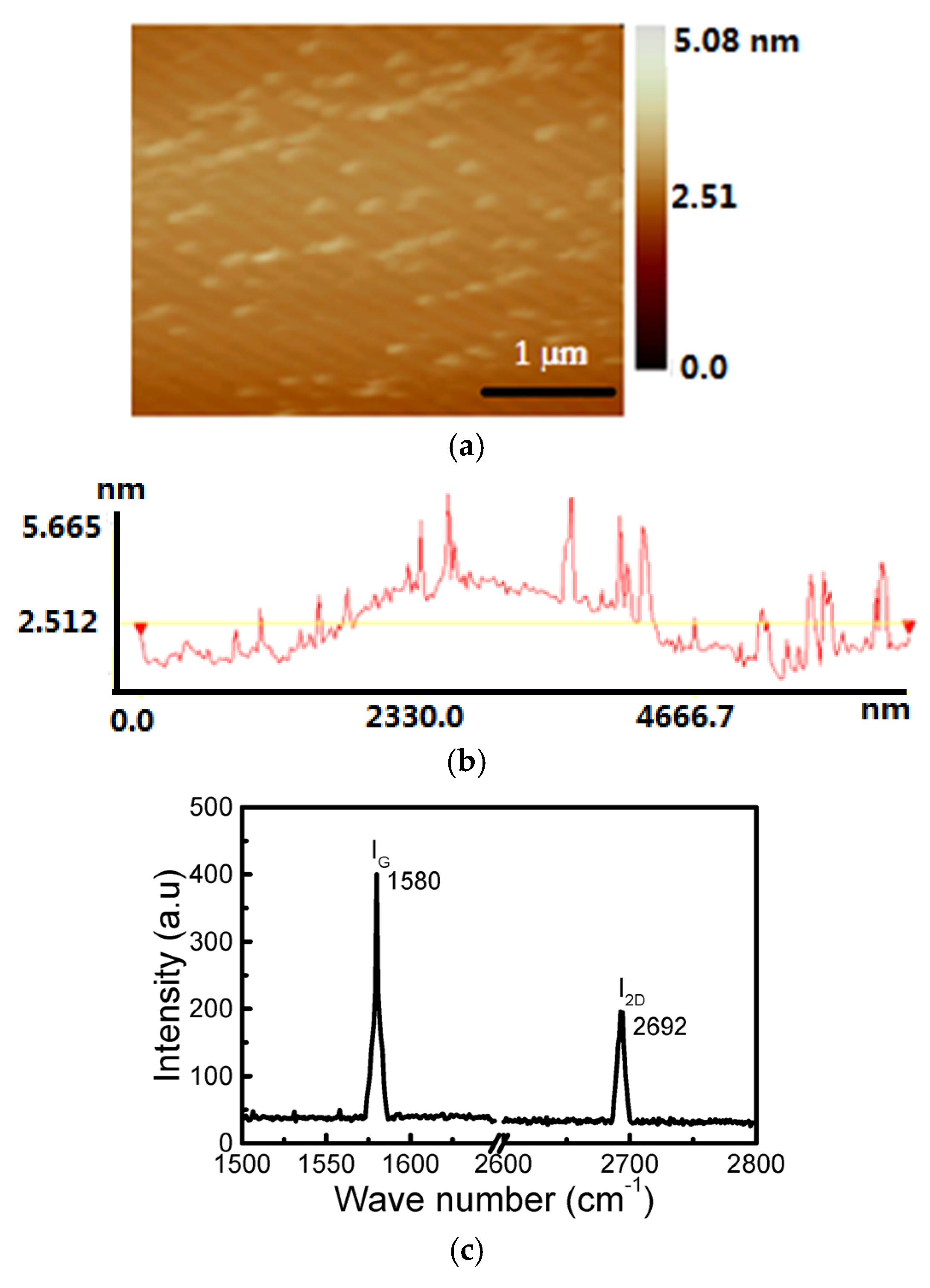
Figure 3.
(a) The AFM image of MoS2 film deposited on Si substrate; (b) the Raman spectrum of MoS2.

Figure 4.
(a) The transmittance the visible light range of the graphene sample; (b) the UV-Vis absorption spectra of the MoS2/Si heterojunction sample in the wavelength range 250–900 nm.
Figure 4.
(a) The transmittance the visible light range of the graphene sample; (b) the UV-Vis absorption spectra of the MoS2/Si heterojunction sample in the wavelength range 250–900 nm.
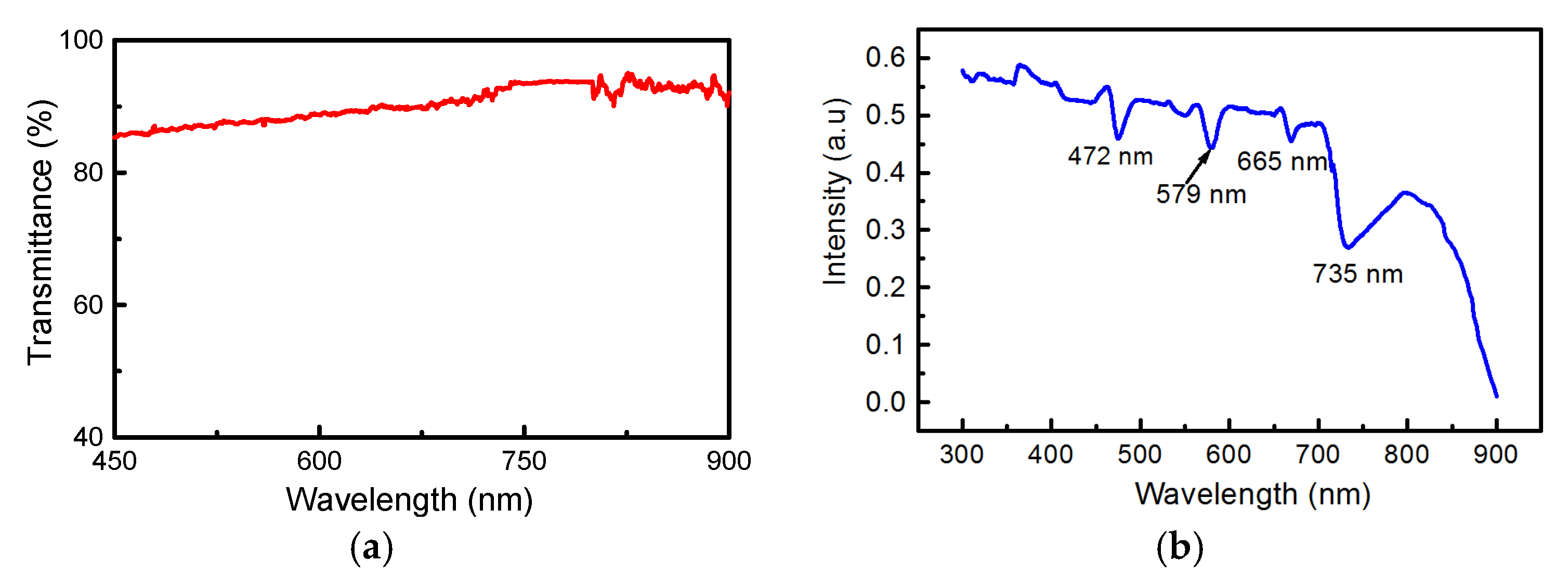
Figure 5.
The current-voltage (I–V) curve of the graphene/MoS2/Si heterojunctions in darkness (a), and illumination with different light energies (b).
Figure 5.
The current-voltage (I–V) curve of the graphene/MoS2/Si heterojunctions in darkness (a), and illumination with different light energies (b).
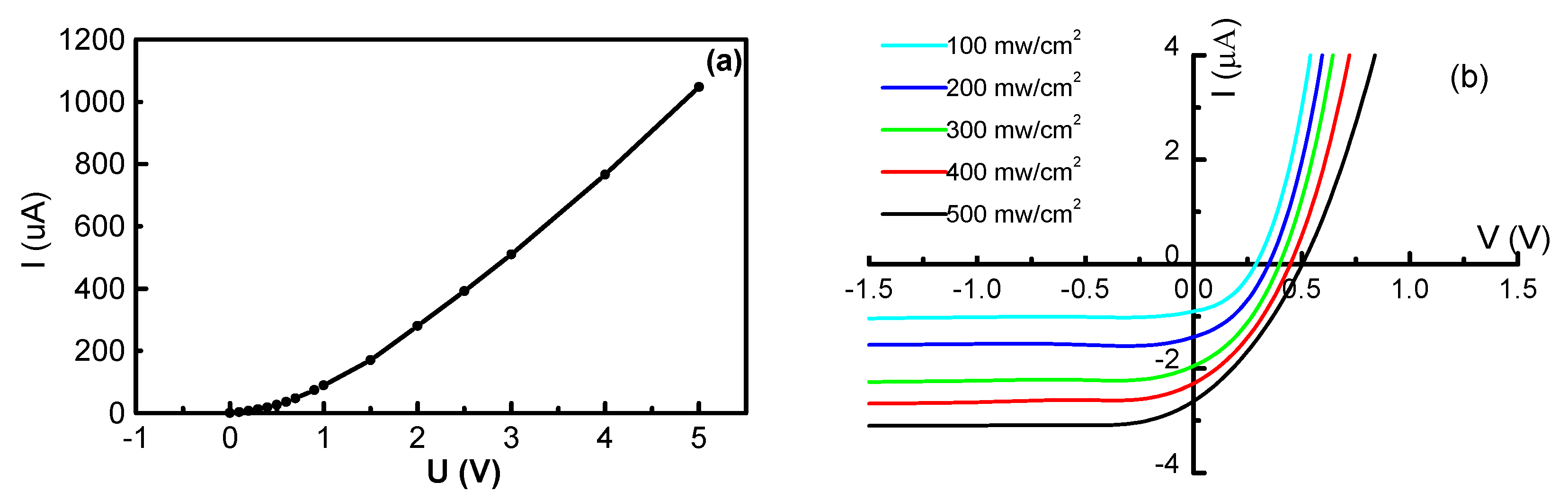
Figure 6.
The parameter dependence of the graphene/MoS2/Si heterojunctions with optical power density: (a) The short-circuit current (ISC); (b) the open-circuit voltage (VOC).
Figure 6.
The parameter dependence of the graphene/MoS2/Si heterojunctions with optical power density: (a) The short-circuit current (ISC); (b) the open-circuit voltage (VOC).
© 2017 by the authors. Licensee MDPI, Basel, Switzerland. This article is an open access article distributed under the terms and conditions of the Creative Commons Attribution (CC BY) license (http://creativecommons.org/licenses/by/4.0/).
Share and Cite
MDPI and ACS Style
Shi, W.; Ma, X. Photovoltaic Effect in Graphene/MoS2/Si Van der Waals Heterostructures. Coatings 2018, 8, 2. https://doi.org/10.3390/coatings8010002
AMA Style
Shi W, Ma X. Photovoltaic Effect in Graphene/MoS2/Si Van der Waals Heterostructures. Coatings. 2018; 8(1):2. https://doi.org/10.3390/coatings8010002
Chicago/Turabian StyleShi, Weilin, and Xiying Ma. 2018. "Photovoltaic Effect in Graphene/MoS2/Si Van der Waals Heterostructures" Coatings 8, no. 1: 2. https://doi.org/10.3390/coatings8010002
Note that from the first issue of 2016, this journal uses article numbers instead of page numbers. See further details here.