Deposition and Patterning of Polycrystalline Diamond Films Using Traditional Photolithography and Reactive Ion Etching

High Technology Physics Research Institute, Tomsk Polytechnic University, Tomsk 634050, Russia
*
Author to whom correspondence should be addressed.
Coatings 2017, 7(9), 148; https://doi.org/10.3390/coatings7090148
Submission received: 31 July 2017
/
Revised: 7 September 2017
/
Accepted: 8 September 2017
/
Published: 15 September 2017
(This article belongs to the Special Issue Diamond and Diamond-Like Coatings: Deposition, Characterization, and Applications)
Abstract
:Given the exceptional characteristics of diamond films, they have become increasingly popular in the fields of medicine, microelectronics, and detector electronics. However, despite all the advantages, there are many technological problems that complicate their widespread application and impose limitations on diamond use in technological processes. In this study, we proposed a new technique for obtaining a complex topology of polycrystalline diamond coatings by selective seeding of the substrate by nucleation centers and subsequent surface treatment with reactive ion etching to reduce the number of parasitic particles. As a result, diamond films were obtained with a high particle concentration in the film region and high repeatability of the pattern. Moreover, parasitic particles influenced neutralization in areas where film coverage was not needed. The effect of the diamond nanoparticle concentration in a photoresist and the effect of reactive ion etching on the formation of a continuous film and the removal of parasitic nucleation centers were examined. The relative simplicity, low power consumption, and high efficiency of this method make it attractive for both industrial and scientific applications.
Keywords:
diamond; CVD; selective; pattern; films; deposition; parasitic particles; reactive ion etching; photolithography1. Introduction
It is well known that diamond coatings are materials with a high potential for future applications. These materials have become increasingly popular because of their wide range of unique characteristics [1,2,3]. Despite these advantages, there are many technological problems that complicate the widespread use of diamond coatings and impose a restriction on their use in technological processes (such as obtaining the necessary topology and dimensions for manufacture of the matrix radiation detectors and diamond RF (radio-frequency) electronics) [4,5]. Because of the synthesis-specific and high complexity of processing single-crystal diamond (such as a strong chemical and wear resistance), the creation of electronic structures with complex geometry using diamond is complex and not suitable for mass production or industrial processes [1,2,6]. As a result, developments are being made in the field of polycrystalline rather than single crystal coatings. The problem of diamond coating deposition over a large area can be effectively solved by using homo- and hetero-substrates such as silicon [1]. However, the problem of treatment remains relevant; although the obtained structures have slightly different properties from monocrystalline diamond, their resistance does not undergo any special changes, except for the brittleness of the material. This problem is especially acute in the field of obtaining coatings with complex topology, microelectronics, and matrix detectors. Moreover, it should be noted that most of the methods used to obtain the geometry (e.g., chemicals, mask use and laser treatment) are technologically inapplicable for diamond coatings. The high resistance to chemical treatment does not allow for the use of the classical chemicals, and effective analogues are too strong and have a highly negative effect on neighboring layers, which are less resistant to such effects. A high diamond density and strong bonds between crystallites (despite the presence of the sp2 phase) do not allow for the use of reverse mask methods (lift-off stencils) [7]. The method of hybrid masks [8] can also be used to obtain the topology, but our goal is to simplify the process as much as possible and to reduce the number of layers and operations used to a minimum. The difference lies in the fact that the pattern is determined even before the growth of the diamond film, which eliminates the need to process the diamond coating itself. The use of laser coating treatment is limited to surface treatment (ablation) [9] and the cutting of finished devices and structures because high beam powers result in the low depth control of etching, and the combination with the heterogeneity of the structure in height and crystal orientation leads to a negative effect on the whole process.
Diamond coatings need to be deposited with high accuracy, but with minimal impact on adjacent layers. The optimal method will be able to obtain coatings with a predetermined pattern by using minimal processing/removal operations and a minimal influence on any adjacent layers.
In previous works [10], we considered a technique for obtaining such coatings by the selective seeding of the substrate with diamond nanoparticles and the subsequent growth of the film on this basis and no more surface treatments have been carried out. The nanodiamond nucleation centers remain due to Van-der-Waals forces and defects on the surface. This occurs during the plate preparation and application of a photoresist pattern with the addition of diamond nanoparticles. The presence of these particles causes the creation of parasitic nucleation centers for the future growth of diamond in the areas where the films should not grow. Therefore, in areas that do not require diamond growth, islets and grains of the diamond are formed, which is highly undesirable, since such inclusions negatively affect the resolution of the pattern and the subsequent characteristics and the potential for uses of the films. It is clear that a higher concentration of nanoparticles in the photoresist leads to the formation of a continuous film earlier, but the resolution of the whole pattern decreases accordingly. Moreover, one of the important factors in the use of any technique is its processability, a shorter deposition time and a stable result plays an important role in determining the technology that will be used later.
In this study, we propose a new technique for obtaining a topology of polycrystalline diamond coatings using the technology of substrate selective seeding by the nucleation centers and subsequent surface treatment with reactive ion etching to reduce the number of parasitic particles.
2. Materials and Methods
2.1. Sample Preparation
We used mirror-polished silicon wafers (111) as substrates for diamond films. Each sample was a disc of Ø76 mm × 350–400 μm. All samples were previously cleaned from organic and inorganic contaminants by washing in an ultrasonic bath in acetone of special purity OP-2. Ultrasonic cleaning was performed at 50 kHz for 5 min. Subsequently, the samples were dried in a nitrogen stream of 99.999% purity until completely dry. The cleaning operation was then repeated in deionized water of 99.99999% purity in an ultrasonic bath at 50 kHz for 7 min.
2.2. Photoresist Preparation and Deposition
To prepare a special photoresist for selective seeding with diamond nanoparticles [10,11] at 5, 10, and 15 (wt %) of a 3% water diamond suspension with a nanoparticle size of 3–9 nm was added to the positive photoresist (PP) (SP-051SHU-05). Stirring was carried out until a homogeneous mass was obtained. The concentration of nanodiamond particles in the photoresist was 0.15, 0.3, and 0.45 (wt %) for seeds of 5, 10, and 15 wt %, respectively. The photoresist was applied to the silicon substrates by the centrifugation method. When the volume of the suspension in the photoresist is relatively large, the photoresist properties will degrade, resulting in a decrease in its ability to polymerize. With a lack of suspension in the photoresist volume, the concentration of diamond nanoparticles becomes so small that it is impossible to continue to obtain continuous films, as shown below. The concentration of diamond powder in the seed should be sufficient to provide the required amount of diamond phase in the suspension, but excessive increases lead to the formation of numerous agglomerates that create microdefects in the film.
The silicon plates were then dried in a thermo-cupboard at a temperature of 70–90 °C to set the photoresist [10]. The substrates were aligned with photomask (PM) followed by layer (AMK 2104.16, SORENG, St. Petersburg, Russia) by UV with λ = 250–440 nm. The photo layer was developed in an alkaline solution of KOH. Furthermore, the photoresist layer was additionally exposed to plasma etching in a nitrogen atmosphere. At the final stage, the resulting silicon wafer was dried in a thermo-cupboard at a temperature of 120–140 °C (Figure 1). To remove parasitic nanodiamond particles, the substrate was subjected to reactive ion etching.
2.3. Reactive Ion Etching
The chamber was evacuated until a pressure of 2 ± 0.2 × 10⁻⁴ Torr, after which purified argon with 99.999% purity was fed through the gas inlet in a flow of 4 mL/min (Bronkhorst EL-FLOW, Ruurlo, The Netherlands), and by adjusting the evacuated flow from the chamber a pressure of 4.3 ± 0.2 × 10⁻⁴ Torr. Under these parameters, the vacuum chamber was maintained for 5 min to eliminate the accumulated gas from the atmosphere in the pores of the chamber and to generate the ion source.
The current density of the ion beam was 1.25 mA/cm2 with an energy of 3.3 ± 0.01 keV [12,13]. Subsequently, the substrate surface was etched in a time range from 30 s to 30 min (Figure 2a). The current was set automatically with the power setting and could vary from changes in chamber pressure, gas flow jumps, etc. The substrate temperature during etching was maintained at 23 ± 2 °C using an IR thermal imager (ULIRvision TI170, Zhejiang ULIRVISION Technology Co., Ltd., Zhejiang, China). After the etching process, the chamber was blown away from residual etch particles for 5 min with the same parameters. As a result of ion etching, we obtained regions consisting of an etched photoresist enriched with nanodiamond particles and a region free of parasitic particles.
2.4. Deposition of Diamond Films
A specialized CVD reactor, based on the known method of “hot filaments” [14,15], was used to deposit the films. In this method, the activation of the gas mixture (H2:CH4) is carried out thermally, by means of incandescent tungsten filaments. The synthesis of diamond films was conducted in a self-made HFCVD reactor (Figure 2b). The atmosphere consisted of H2:CH4 (100:6; purity of gases: H2, 99.9999%; CH4, 99.99%) with a total gas flow rate of 106 mL/min. The distance between hot tungsten filaments (Ø0.2 mm × 10 cm) and substrates was 10 ± 0.5 mm. The sagging of threads was eliminated by the system of constant tension of the threads. The substrate temperature during deposition was maintained at 900 ± 25 °C using an IR thermal imager. The reactor pressure was 20 ± 1 Torr (Pfeiffer Vacuum CMR 372, Pfeiffer Vacuum GmbH, Asslar, Germany), and the filament current was 6.5 ± 0.01 A per filament. The filament temperature was maintained at 2200 ± 35 °C using an Infrared Non-Contact Pyrometer (AST A250 PL/TL, Accurate Sensors Technologies Ltd., Rajasthan, India). The photoresist during the deposition process is completely sublimed and removed from the surface of the substrate, leaving only diamond nanoparticles seeded in the required regions. The average growth rate of a continuous diamond film with columnar microstructure was 1 μm/h. The deposition time of the film for all samples was 2 h. The film thickness was in the range of (2–3) ± 0.3 μm.
2.5. Characterization
The surface morphologies and grain structure of the films, as well as nucleation density (Nd), were analyzed by scanning electron microscopy (SEM) using an Quanta 3D SEM (FEI, Hillsboro, OR, USA) and VEGA3 SB (TESCAN, Brno-Kohoutovice, Czech Republic) without the sputtering of any conductive film. The samples were characterized by X-ray diffraction (XRD) using Cu-Kα radiation on a Shimadzu XRD-6000 diffractometer (Shimadzu Scientific Instruments (SSI), Columbia, MD, USA). Raman spectra were recorded on a NanoScan Technology Centaur I HR spectrometer (LLC “Nano Scan Technologies”, Moscow, Russia).
Nucleation density was determined by counting the number of crystallites on SEM photomicrographs (after their respective digital processing). Each value of Nd was obtained by averaging the count data into 10 pictures in different regions of each of the samples.
3. Results
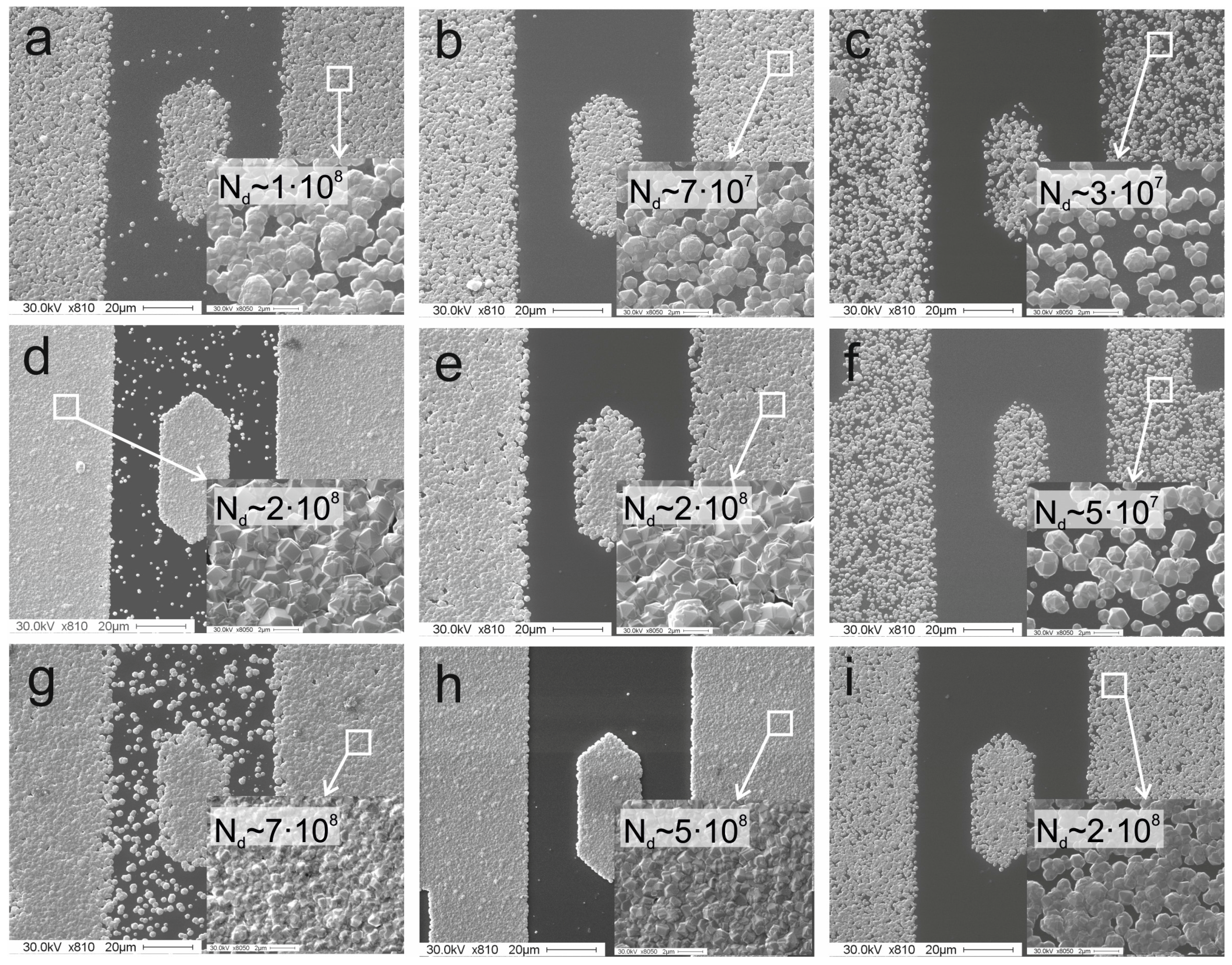
Figure 3 shows the dynamics of the change in the density and character of nucleation at different durations of ion etching of the photoresist and various initial concentrations of diamond nanoparticles in the photoresist. Without ion etching, the nucleation density was sufficiently high and was largely determined by the initial content of the diamond nanoparticles in the photoresist. An increase in the concentration of diamond nanoparticles in the volume of the photoresist also led to a higher relative area of the film coating (the area bounded by the geometry of the topology, which is covered by the film of parasitic particles (ηp) and of the coating (ηf)). For example, ηf shows that the film can cover only 80% of the required area. It is evident that there was a high percentage of parasitic nucleation centers in the region that did not require a film covering. Moreover, with an increase in the initial concentration of diamond nanoparticles in the volume of the photoresist, the number of parasitic nucleation centers increased regularly, which reduced the topology resolution. These crystallites may have formed because some of the nanodiamonds still remained on the silicon when the photoresist was washed off in non-illuminated areas. This retention is due to defects on the surface of the coating and weak Van-der-Waals forces, and, when deposited, the nanodiamonds become centers of “parasitic” crystallite nucleation. This effect is enhanced by increasing the concentration of nanodiamond in the photoresist, which is confirmed by the comparison of Figure 3a,d,g; (at nanodiamond concentrations of 0.15, 0.30, and 0.45 wt %, respectively).
At the same time, at a diamond particle concentration of 0.15 wt %, (Figure 3a), a continuous film was not formed even without the use of reactive ion etching, which makes that concentration unsuitable and precludes its use in the future. Samples for which selective seeding was carried out with a low content of nanodiamonds require much more time to form a continuous film, so the average crystallite size in such films will be much larger, which seriously reduces the resolution of this method. Reducing the ηf below 97% leads to the formation of large voids in the film, leading to a deterioration in its electrophysical characteristics.
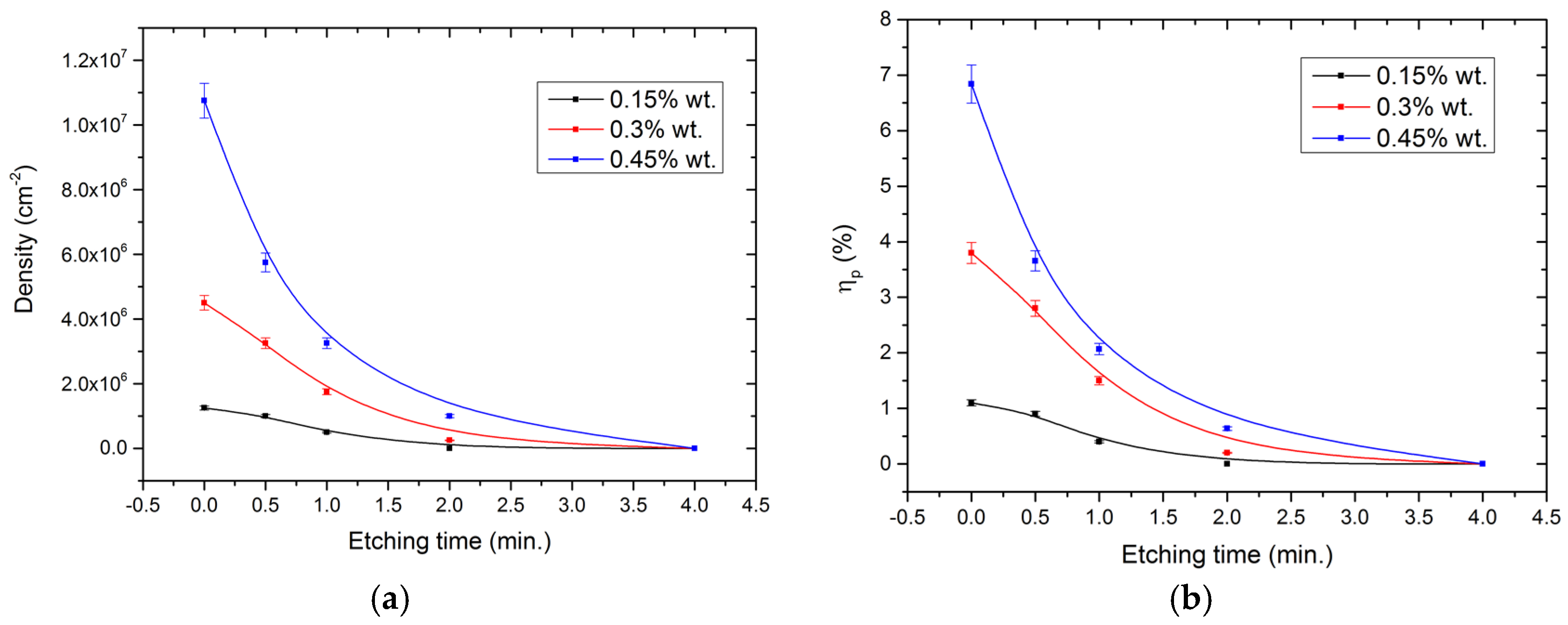
We found that, as the duration of reactive ion etching increased, in addition to reducing the number of parasitic particles, the density of nucleation and ηf also decreased. Figure 4a shows how the density of nucleation particles changed with the increase in the duration of reactive ion etching, and a considerable decrease in nucleation density was observed at low etching durations (less than 7 min). Further increases in the etching duration no longer decreased the diamond Nd. Figure 4b shows how the ηf changed with the increase in the duration of ion etching, it is also evident that the percentage decreased strongly at etching durations less than 7 min, and there was further decline in the rate of change even at sufficiently high etching periods. The ηf index is related to the Nd, but it also takes into account the change in the crystallite size and the geometric pattern of topology, as the distance between the nucleation centers. As a result of the free space around them, the crystallites did not grow upwards only. This led to an increase in the transverse dimension of the crystal and may also affect the probability of creating agglomerates of their particles.
The concentration of parasitic particles is also strongly reduced in the time range from 30 s to 4 min (Figure 5), after which only isolated particles were present. In these cases, the regularity in the appearance of parasitic particles cannot be revealed, and no overall concentration can be estimated. A strong influence of the ratio of nanodiamond particles in suspension to the growth of parasitic crystals was also observed, as well as the effect of reactive ion etching. Of course, it is worth noting that the parameters of the etching duration strongly depends on the etching parameters themselves, and it is possible to use a wide range of ion sources with different operating parameters, operating principles, and operating power to obtain the effect under consideration. The main feature here is the process of etching of diamond particles from areas cleaned of photoresist. With the described parameters of all samples at an etching time of more than 4 min, they were cleared of particle parasite influence (Table 1).
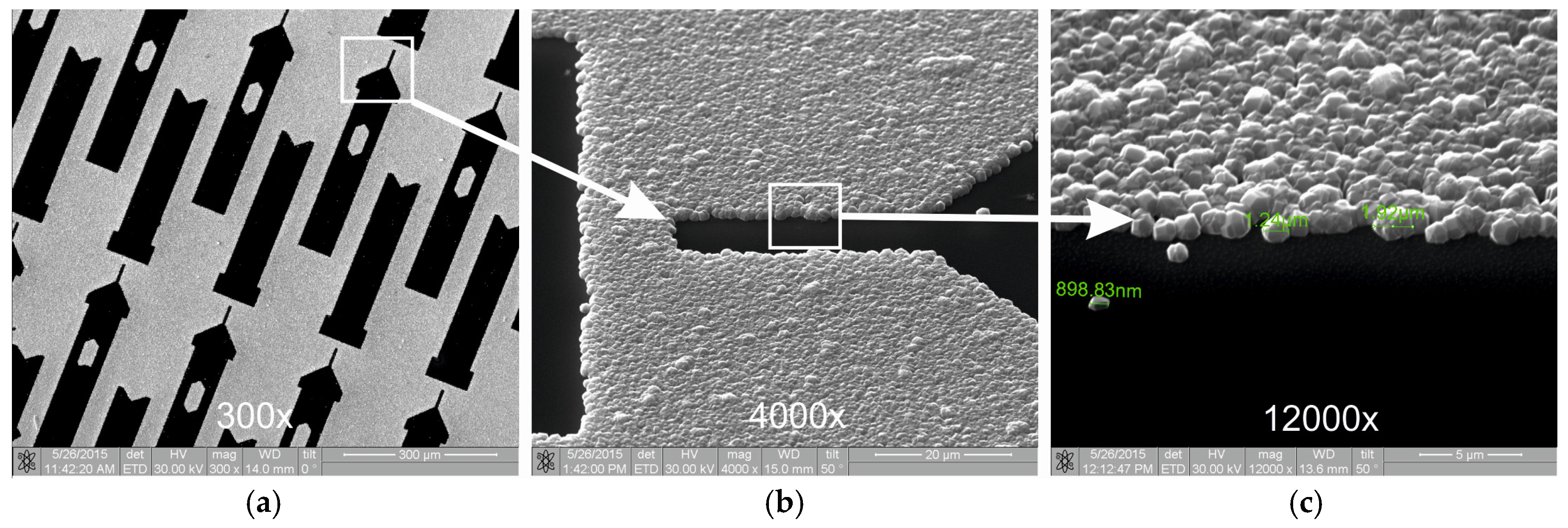
Figure 6 shows the resulting topology of the surface when using a photoresist with a diamond nanoparticle concentration of 0.45 wt % and an etching time of 4 min. The resolution of this method is mostly limited by the size and shape of the crystallites themselves, while the area that does not require film growth retained a surface clean from seeding and subsequent diamond film deposition.
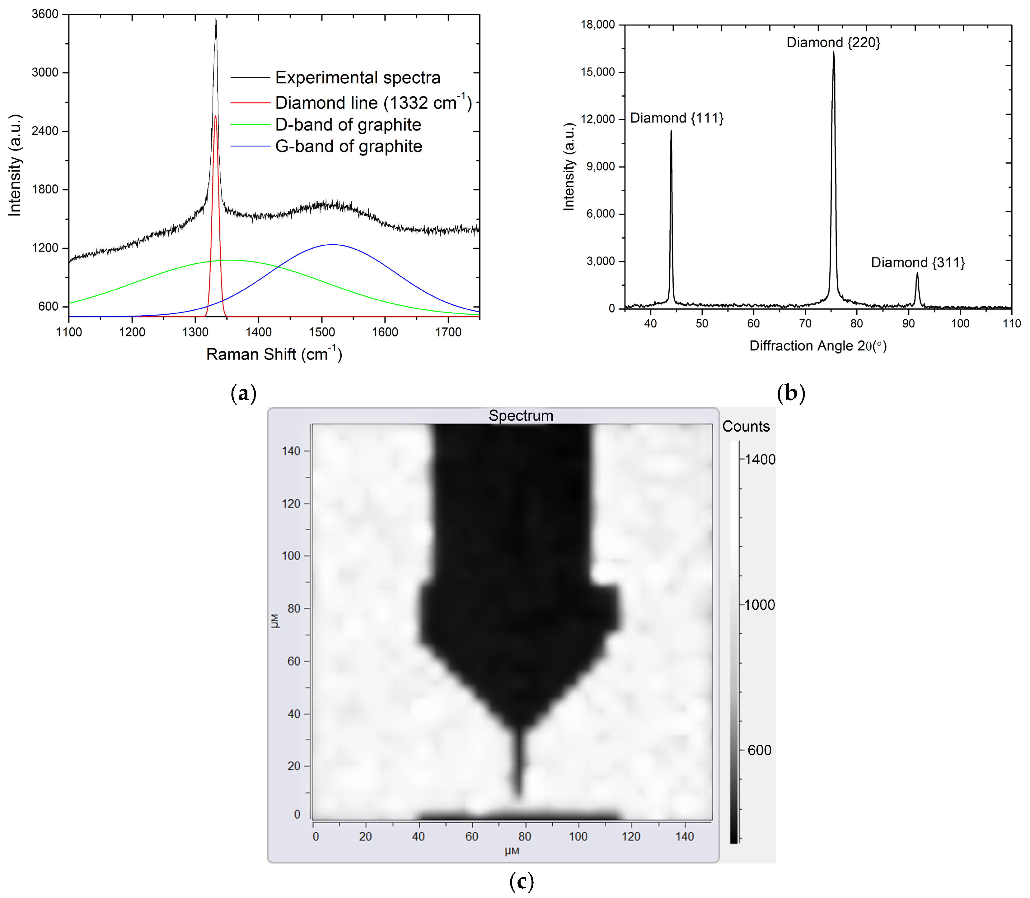
Figure 7 shows Raman (Figure 7a) and X-ray diffraction (Figure 7b) spectra of the deposited diamond films. X-ray diffraction peaks at 44.0°, 75.5°, and 91.8° correspond to the (111), (220), and (311) diamond planes, respectively. Narrow diffraction lines show the absence of an appreciable amount of the amorphous and nanodiamond phase in the films. Figure 7c shows the continuity of the film by a Raman map.
The obtained Raman spectra indicate that the film was a polycrystalline diamond (diamond line 1332 cm−1) of a sufficiently high degree of purity with a small fraction of the impurities of sp2 carbon (D and G bands of graphite) [16,17]. All the deposited diamond films had a classical single-layer columnar structure without a pronounced crystallite texture.
4. Discussion
In the current work, we demonstrated a new technique for the selective deposition of diamond coatings using classical photolithography with the addition of diamond nanoparticles and subsequent reactive ion etching to remove the influence of parasitic particles. This technology showed the effect of the amount of diamond nanoparticles in the photoresist on the appearance of parasitic particles, as well as the effect of processing by reactive ion etching and its efficiency in reducing the number of nucleation centers in areas that did not require film coverage. The described technique of seeding, cleaning with reactive ion etching, and the subsequent deposition of a diamond coating showed a high efficiency for obtaining a predetermined topology of a polycrystalline diamond film, without the need of different sublayers, aggressive etchants, or laser processing. The relative simplicity, low power consumption, and high efficiency of this method make it attractive for both industrial and scientific applications.
Acknowledgments
The research is funded from Government Task “SCIENCE” Grant Number 2.9223.2017/8.9, the experimental calculations are carried out at Tomsk Polytechnic University within the framework of Tomsk Polytechnic University Competitiveness Enhancement Program grant.
Author Contributions
Stepan Linnik and Vitalii Okhotnikov conceived and designed the experiments; Stepan Linnik performed the experiments; Vitalii Okhotnikov and Alexander Gaydaychuk analyzed the data; Alexander Gaydaychuk worked with reagents/materials/analysis tools; Stepan Linnik and Vitalii Okhotnikov wrote the paper.
Conflicts of Interest
The authors declare no conflict of interest.
References
- Asmussen, J.; Reinhard, D.K. Deposition chemistry: Deposition pathways, nucleation, and growth. In Diamond Films Handbook; Asmussen, J., Reinhard, D.K., Eds.; Marcel Dekker, Inc.: New York, NY, USA; Basel, Switzerland, 2002; pp. 63–219. [Google Scholar]
- Niall, J.T. Diamond Based Nanostructures for Electronic Applications. Ph.D. Thesis, University of London, London, UK, 2010. [Google Scholar]
- Bigelow, L. Diamond coatings. J. Phys. 1993, 3, 897–902. [Google Scholar] [CrossRef]
- Friedl, M. Diamond Detectors for Ionizing Radiation. Master’s Thesis, University of Technology, Vienna, Austria, January 1999. [Google Scholar]
- Gurbuz, Y.; Esame, O.; Tekin, I.; Kang, W.P.; Davidson, J.L. Diamond semiconductor technology for RF device applications. Solid State Electron. 2005, 49, 1055–1070. [Google Scholar] [CrossRef] [Green Version]
- Davidson, J.L.; Ellis, C.; Ramesham, R. Selective deposition of diamond films. J. Electron. Mater. 1989, 18, 711–715. [Google Scholar] [CrossRef]
- Zhang, J.; Zhou, M.; Wu, W.; Tang, Y. Fabrication of diamond microstructures by using dry and wet etching methods. Plasma Sci. Technol. 2013, 15, 1–4. [Google Scholar] [CrossRef]
- Ghoneim, M.; Hussain, M.M. Highly Manufacturable Deep (Sub-Millimeter) Etching Enabled High Aspect Ratio Complex Geometry Lego-Like Silicon Electronics. Small 2017, 13, 1601801. [Google Scholar] [CrossRef] [PubMed]
- Komlenok, M.S.; Kononenko, V.V.; Ralchenko, V.G.; Pimenov, S.M.; Konov, V.I. Laser induced nanoablation of diamond materials. Phys. Procedia 2011, 12, 37–45. [Google Scholar] [CrossRef]
- Okhotnikov, V.V.; Linnik, S.A.; Gaydaychuk, A.V. Selective deposition of polycrystalline diamond films using photolithography with addition of nanodiamonds as nucleation centers. IOP Conf. Ser. Mater. Sci. Eng. 2016, 116, 1–7. [Google Scholar] [CrossRef]
- Lin, C.; Chang, H.; Ben Dao, M.; Chiang, H.H.; Chen, W. Fabrication of antireflection nanodiamond particle film by the spin coating deposition technique. Int. J. Photoenergy 2014, 2014, 87–92. [Google Scholar] [CrossRef]
- Okhotnikov, V.V.; Linnik, S.A.; Gaydaychuk, A.V. The research of diamond coatings morphology evolution under the action of reactive ion etching in perpendicular direction. Key Eng. Mater. 2016, 712, 87–92. [Google Scholar] [CrossRef]
- Okhotnikov, V.V.; Linnik, S.A.; Gaydaychuk, A.V. Research of reactive ion and plasma-chemical etching effect on diamond coating surface morphology. AIP Conf. Proc. 2016, 1772, 040007. [Google Scholar]
- Hirabayashi, K.; Taniguchi, Y.; Takamatsu, O.; Ikeda, T.; Ikoma, K.; Iwasaki-Kurihara, N. Selective deposition of diamond crystals by chemical vapor deposition using a tungsten-filament method. Appl. Phys. Lett. 1988, 53, 1815–1817. [Google Scholar] [CrossRef]
- Hu, J.; Foord, J.S.; Holt, K.B. Hot filament chemical vapor deposition of diamond. Phys. Chem. 2007, 9, 5469–5475. [Google Scholar] [CrossRef]
- Ferrari, A.C.; Robertson, J. Raman spectroscopy of amorphous, nanostructured, diamond-like carbon, and nanodiamond. Philos. Trans. R. Soc. London A Math Phys. Eng. Sci. 2004, 362, 2477–2515. [Google Scholar] [CrossRef] [PubMed]
- Wang, W.N.; Fox, A.; May, P.W.; Knapper, M.P.; Meaden, G.; Partridge, P.G.; Ashfold, N.R.; Steeds, W.; Hayward, P.; Pitt, D. Laser Raman studies of polycrystalline and amorphic diamond films. Phys. Stat. Sol. 1996, 154, 255–268. [Google Scholar] [CrossRef]
Figure 1.
The technological route of obtaining a diamond coating pattern.
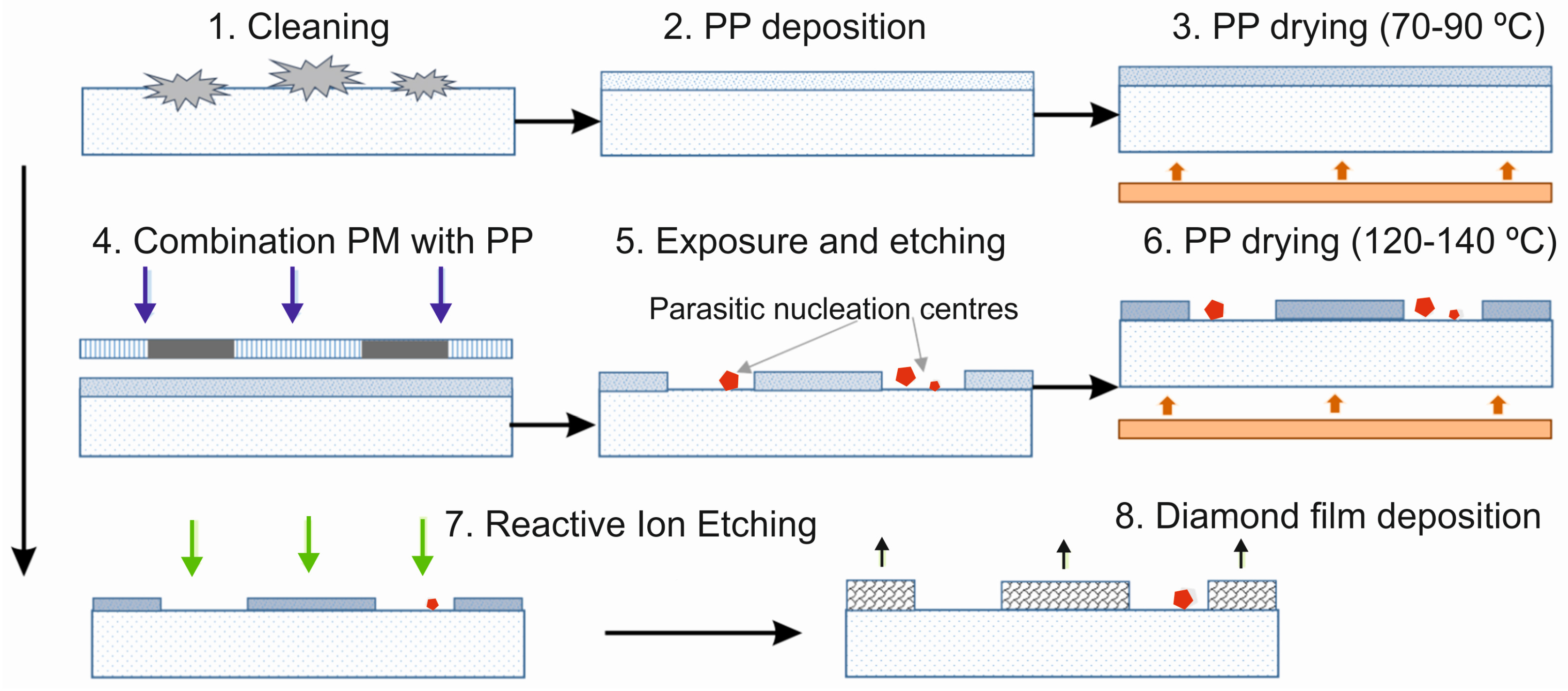
Figure 2.
Schematic of (a) the reactive ion etching process; (b) the HF-CVD reactor.
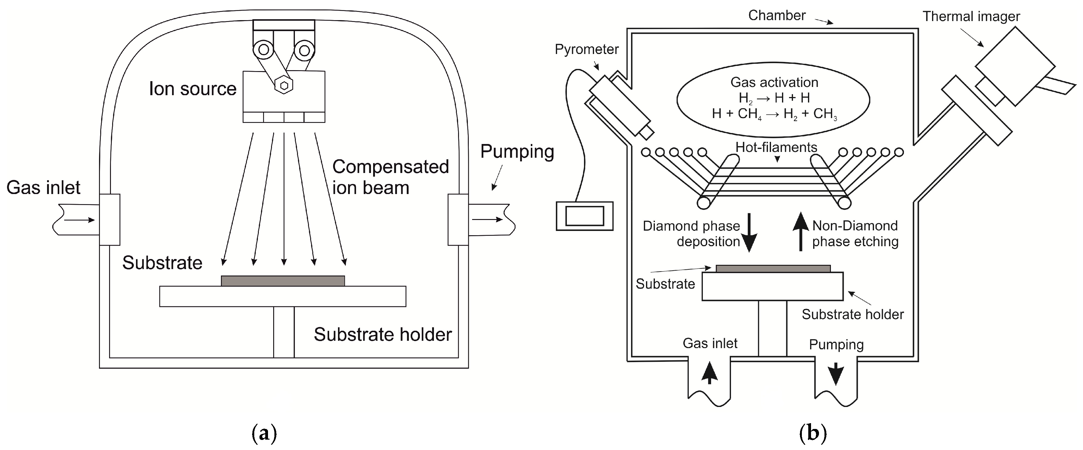
Figure 3.
SEM images of the diamond film topography surface seeding by (a–c) 0.15 wt % of nanodiamond in photoresist, (d–f) 0.3 wt %, (g–i) 0.45 wt % and with different durations of reactive ion etching: (a,d,g) without etching; (b,e,h) 4 min; (c,f,i) 30 min.
Figure 3.
SEM images of the diamond film topography surface seeding by (a–c) 0.15 wt % of nanodiamond in photoresist, (d–f) 0.3 wt %, (g–i) 0.45 wt % and with different durations of reactive ion etching: (a,d,g) without etching; (b,e,h) 4 min; (c,f,i) 30 min.

Figure 4.
Nucleation particle density (a) and relative area of the film coating (b) for pattern area with diamond films depending on etching time.
Figure 4.
Nucleation particle density (a) and relative area of the film coating (b) for pattern area with diamond films depending on etching time.
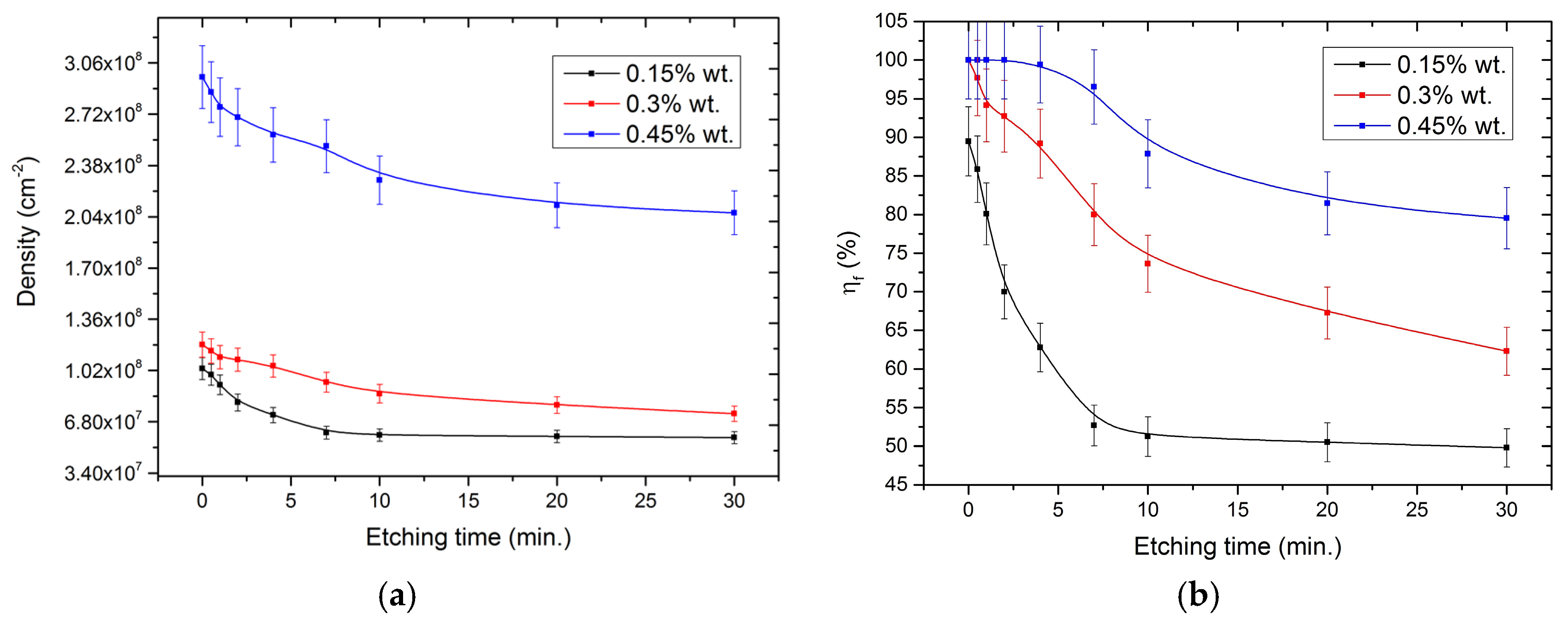
Figure 5.
Nucleation particle density (a) and relative area of parasitic particles (b) against etching time in regions without a film.
Figure 5.
Nucleation particle density (a) and relative area of parasitic particles (b) against etching time in regions without a film.

Figure 6.
SEM image of the produced film (0.45 wt % of nanodiamond particles in photoresist and 4 min treatment by reactive ion etching) edge with different magnifications: (a) 300×, (b) 4000×, and (c) 12,000×.
Figure 6.
SEM image of the produced film (0.45 wt % of nanodiamond particles in photoresist and 4 min treatment by reactive ion etching) edge with different magnifications: (a) 300×, (b) 4000×, and (c) 12,000×.

Figure 7.
Raman (a) and X-ray diffraction (b) spectra of diamond film; (c) Raman mapping.


Table 1.
Effect of reactive ion etching on the concentration of parasitic particles in regions without a film.
Table 1.
Effect of reactive ion etching on the concentration of parasitic particles in regions without a film.
| Time (min) | 0.15 (wt %) | 0.30 (wt %) | 0.45 (wt %) | |||
|---|---|---|---|---|---|---|
| Density, cm−2 | ηp, % | Density, cm−2 | ηp, % | Density, cm−2 | ηp, % | |
| 0 | 1.3 × 10⁶ | 1.1 | 4.5 × 10⁶ | 3.8 | 1.1 × 10⁷ | 6.8 |
| 0.5 | 1.0 × 10⁶ | 0.9 | 3.3 × 10⁶ | 2.8 | 5.8 × 10⁶ | 3.7 |
| 1 | 5.0 × 10⁵ | 0.4 | 1.8 × 10⁶ | 1.5 | 3.3 × 10⁶ | 2.1 |
| 2 | 0.00 | 0.0 | 2.5 × 10⁵ | 0.2 | 1.0 × 10⁶ | 0.6 |
| 4 | 0.00 | 0.0 | 0.00 | 0.0 | 0.00 | 0.0 |
© 2017 by the authors. Licensee MDPI, Basel, Switzerland. This article is an open access article distributed under the terms and conditions of the Creative Commons Attribution (CC BY) license (http://creativecommons.org/licenses/by/4.0/).
Share and Cite
MDPI and ACS Style
Linnik, S.; Okhotnikov, V.; Gaydaychuk, A. Deposition and Patterning of Polycrystalline Diamond Films Using Traditional Photolithography and Reactive Ion Etching. Coatings 2017, 7, 148. https://doi.org/10.3390/coatings7090148
AMA Style
Linnik S, Okhotnikov V, Gaydaychuk A. Deposition and Patterning of Polycrystalline Diamond Films Using Traditional Photolithography and Reactive Ion Etching. Coatings. 2017; 7(9):148. https://doi.org/10.3390/coatings7090148
Chicago/Turabian StyleLinnik, Stepan, Vitalii Okhotnikov, and Alexander Gaydaychuk. 2017. "Deposition and Patterning of Polycrystalline Diamond Films Using Traditional Photolithography and Reactive Ion Etching" Coatings 7, no. 9: 148. https://doi.org/10.3390/coatings7090148
Note that from the first issue of 2016, this journal uses article numbers instead of page numbers. See further details here.