1. Introduction
Due to low production costs and decreased operating temperatures, plasma enhanced chemical vapor deposition (PECVD) remains the dominant processing method for the manufacture of silicon thin films in both the solar cell and microelectronic industries [
1,
2,
3]. Given the difficulty of in situ measurements during the deposition of amorphous silicon thin films, numerous groups have developed models to characterize the behavior of PECVD systems. Specifically, gas flow and volumetric chemical reactions within PECVD reactors have been investigated using computational fluid dynamics (CFD) models of varying complexities [
4,
5,
6]. Additionally, the complex chemistry and surface interactions that define the microscopic growth of thin film layers have been modeled [
7,
8,
9,
10] using kinetic Monte Carlo models and such models have been demonstrated to reproduce amorphous silicon films with accurate growth rates and morphologies. Furthermore, significant efforts have been made in linking macroscopic first-principals models of gas phase species concentrations and temperature employing approximate flow field equations with microscopic surface models (e.g., Rodgers, S. and Jensen, K., 1998, Lou, Y. and Christofides, P.D., 2003 and Aviziotis et al., 2016 [
11,
12,
13]). However, macroscopic CFD models that develop an accurate flow field solution without approximation and microscopic surface models have not been linked in the context of PECVD.
Unfortunately, potentially decoupled CFD and surface interaction models are unable to capture phenomena which occur at the boundary (thin film surface) between the two PECVD simulation domains. One such phenomenon, which remains a persistent issue during the manufacture of amorphous silicon thin films, is non-uniformities which develop in the thickness and morphology of deposited layers across the radius of the wafer. Spatially non-uniform deposition has been well characterized [
14,
15,
16] and shown to affect the efficiency of solar cell products [
17], resulting in poor device quality and increased costs [
18]. As such, there exists a need for accurate PECVD reactor models which are capable of predicting the codependent behavior of the macroscopic gas phase and microscopic thin film growth. Multiscale models of this type may provide insight into the root cause of spatial non-uniformities present in the deposition of silicon layers, as well as allow for improved reactor geometries and optimal operating strategies to be developed.
To this end, a multiscale CFD model is proposed in this work which captures the interconnection between the macroscopic and microscopic domains in PECVD systems. This model is applied to the PECVD of
a-Si:H thin films at industrially relevant conditions of
T = 475 K,
P = 1 Torr and a 9:1 ratio of hydrogen to silane gas in the feed. At the macroscopic scale, a structured mesh containing 120,000 cells is used to discretize the chambered reactor geometry. ANSYS Fluent software is used as a framework to solve the governing momentum, mass and energy equations which define the dynamics of the process gas inside the parallel plate PECVD reactor, and to orchestrate the communication between simulation domains. Three user defined functions (UDFs) are implemented in order to tailor the Fluent architecture to the specific application of the deposition of amorphous silicon thin films. The first accounts for the 34 prevalent gas phase reactions, including nine ionization reactions which produce the plasma. A second UDF provides an accurate electron density profile based on the work of Park et al. [
19]. The final and most computationally demanding function comprises a hybrid kinetic Monte Carlo algorithm used to model the complex surface phenomena which characterize the microscopic domain. Additionally, given the significant computational requirements of this work, a novel parallelization strategy is developed and applied to both the reactor mesh and the individual microscopic thin film simulations.
The model described above is applied to the batch deposition of a 300 nm thick a-Si:H thin film. Spatial gradients are shown to develop in the concentration of SiH and H near the surface of the silicon wafer. Consequently, non-uniformities in the thin film thickness and hydrogen content are predicted to exceed 20% and 3%, respectively. These results represent an unacceptable margin from a manufacturing standpoint and highlight the importance of multiscale models in predicting and characterizing the behavior of PECVD reactors such that improved reactor geometries and operating conditions may be achieved.
2. Process Description and Modeling
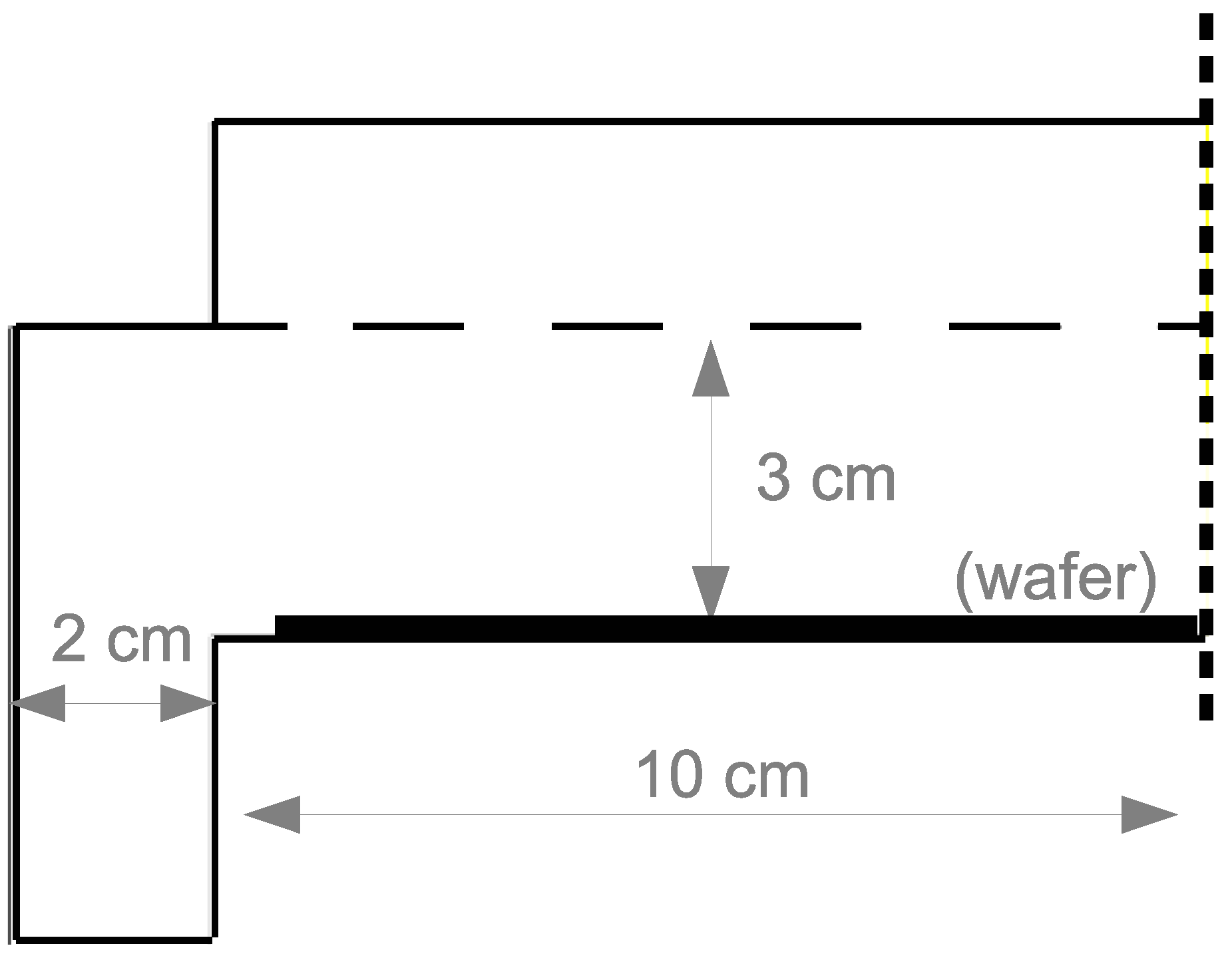
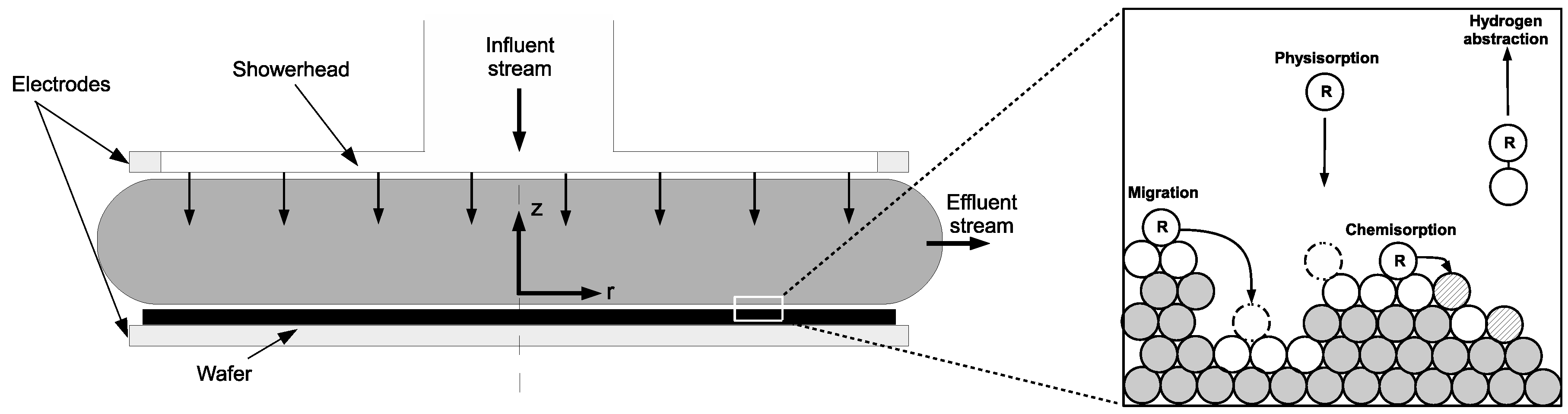
The PECVD reactor utilized in this work belongs to the widely used subclass of CVD reactors known as chambered, parallel-plate reactors. The specific geometry used in this investigation is a cylindrical reaction chamber with a 20 cm wafer capacity and 3 cm showerhead spacing (
Figure 1 and
Figure 2). Process gases are pumped into the inlet at the top of the reactor before being distributed through circular showerhead holes into the reaction zone (light grey region in
Figure 1). Within the reaction zone plasma is produced via a radio frequency (RF) power source across the parallel plate structure. The resulting plasma phase species flow radially outward across the wafer surface, eventually exiting the reactor through outlets near the bottom. The specifics of the plasma chemistry will be provided in the macroscopic modeling section (
Section 2.2 and
Table 1 below).
Two distinct simulation regimes may be specified within the PECVD process: the macroscopic gas phase which can be described by momentum, mass and energy balances, as well as the complex, microscopic surface interactions that dictate the structure of the silicon thin film of interest.
Figure 1 highlights the multiscale character of this process and the need to capture the dynamics at both scales due to the codepedency between the macroscopic and microscopic regimes. The following sections detail both the macroscopic gas-phase model and the microscopic surface model.
2.1. CFD Geometry and Meshing
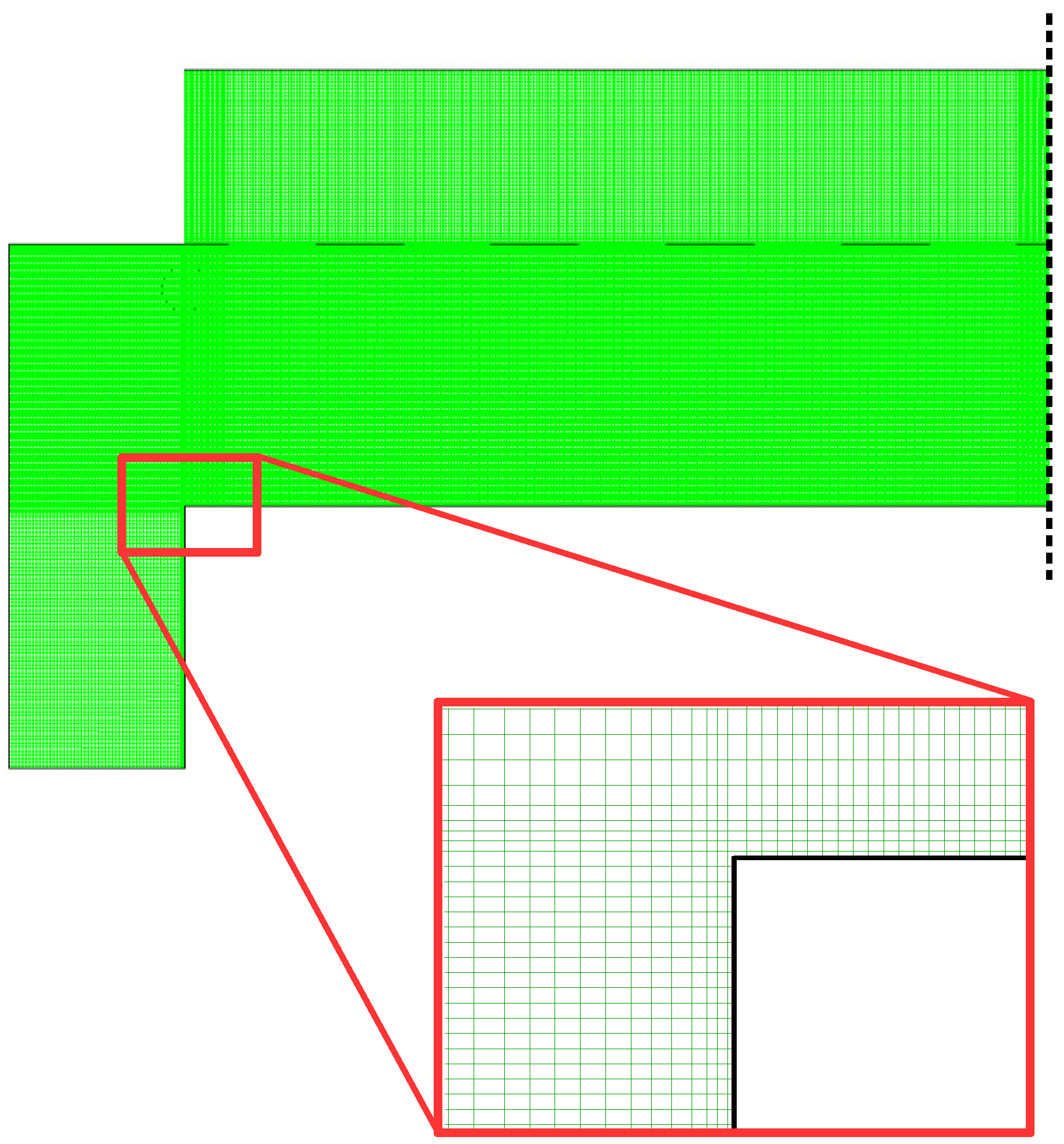
Throughout this work, ANSYS software is utilized for the creation of the geometric mesh (specifically, ICEM meshing) and as a solver for the partial differential equations presented in the following sections (FLUENT version 15.07). As mentioned previously, the chambered PECVD reactor is approximated using a 2D axisymmetric geometry (
Figure 2). Given the difficulty of translating three dimensional showerhead holes into a two dimensional axisymmetric representation, 1 cm gaps are chosen as a simple means by which the inlet gases may flow into the plasma chamber. The results presented in the latter half of this work suggest a good agreement between the observed plasma characteristics and those reported experimentally; consequently, no additional showerhead hole arrangements are explored.
Two general meshing strategies exist for the discretization of a given geometry: (1) structured meshes contain a collection of quadrilateral cells in a specific, repeating pattern; and (2) unstructured meshes are composed of a collection of polygons in an irregular pattern. Simple geometries (i.e., geometries lacking curvature and complex shapes) benefit from the use of a structured mesh as they can provide higher quality, in terms of orthogonality and aspect ratio, while remaining computationally efficient. Given the rectangular character of the 2D axisymmetric PECVD geometry, a structured mesh composed of 120,000 cells is employed. The specific number of cells within the mesh is determined using a mesh-independent study whereby the number of cells is increased until identical results are recorded. Thus, the use of a finer mesh (above 120,000 cells) would provide no benefit to the PECVD model developed here while requiring greater computational resources.
Figure 3 demonstrates the non-uniform cell density within the proposed mesh. Regions in which significant gradients are expected (e.g., gradients in the temperature, species concentration, flow velocity, etc.) contain a higher mesh density. This is of special importance near the showerhead holes and along the surface of the wafer. Accurate flow modeling of the process gas into the reaction zone is crucial in order to obtain plasma distributions which are industrially relevant and which yield representative growth of thin film layers.
Due to the relatively low flow rate of process gas (75 cm/min) and low chamber pressure (1 Torr), the flow along the surface of the wafer is expected to be laminar (note: preliminary flow characteristics from the macroscopic model suggest a Reynold’s number of Re = 2.28 × 10). As a result, the mesh density directly above the wafer surface has been increased such that the boundary layer can be adequately captured.
2.2. Gas-Phase Model
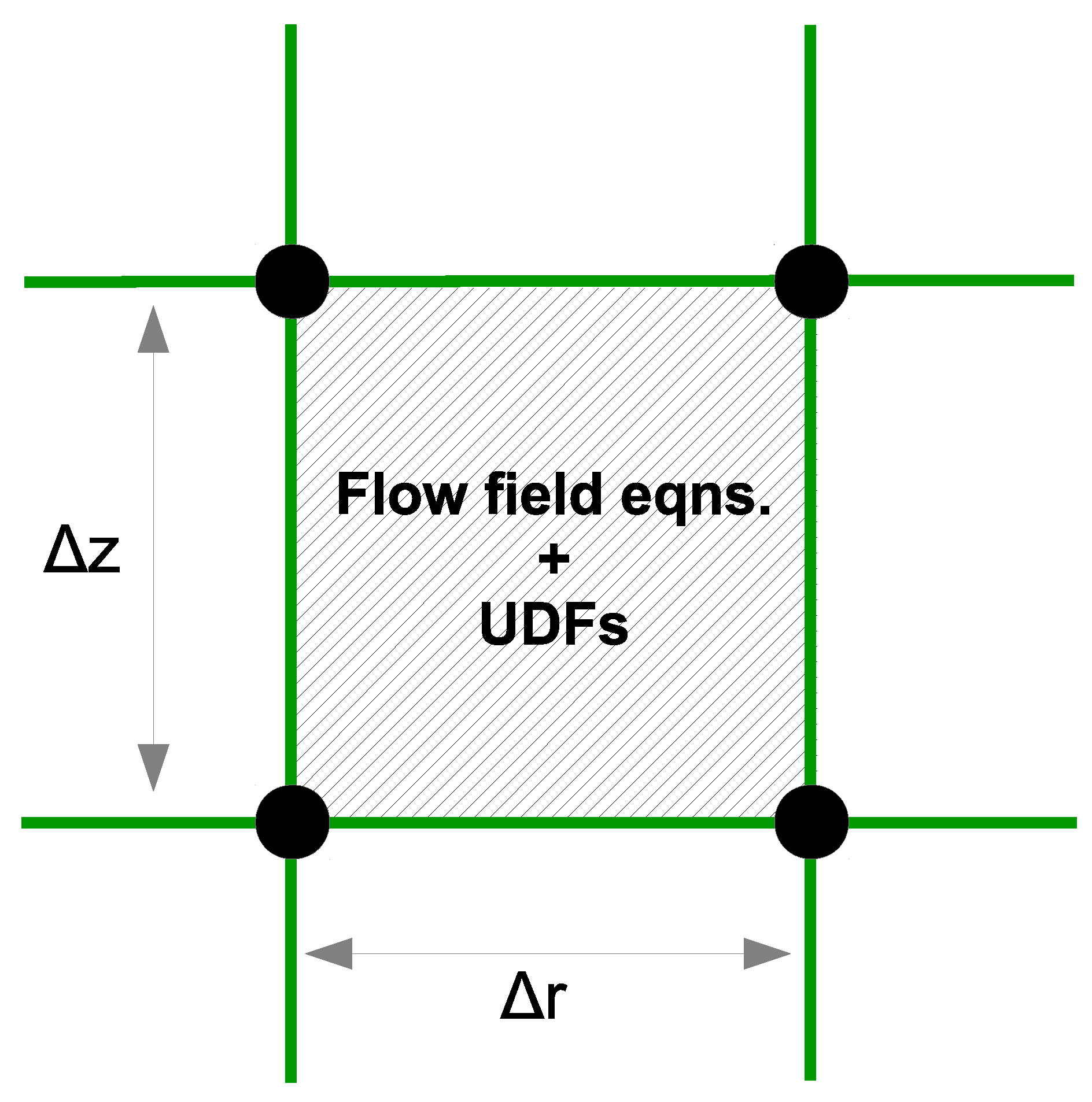
At the macroscopic level, the physio-chemical phenomena that govern the behavior of the gas-phase species are complex in nature. Mass, momentum and energy balances each play a key role in determining the growth of amorphous silicon layers within the PECVD reactor. Consequently, analytic solutions to the gas-phase model are viable only for simplified systems which fail to yield meaningful results. Instead, we employ numerical methods here which are capable of solving the complex fluid dynamics equations with high accuracy within the mesh structure presented in the previous section. At every time step, and for each cell of the mesh (e.g.,
Figure 4), the governing equations are discretized using the ANSYS Fluent solver via finite difference methods. Additionally, user defined functions (UDFs) are applied to each cell which allow for extended functionality of the Fluent framework.
The continuity, energy and momentum equations employed in this work are standard and as such will be presented only briefly. For a more detailed description of the flow field equations, please refer to the Fluent user manual [
20,
21]. In a generalized vector form, the governing equations are given by the following system:
where
ρ is the density of the gas,
is the physical velocity vector,
p is the static pressure,
and
I are the stress and unit tensors,
J is the diffusive flux,
is the mass fraction of species
i,
is the diffusion coefficient of species
i, and
,
and
are user defined terms which will be defined below.
In order to tailor the functionality of the Fluent solver to the specific application of silicon processing via PECVD, three predominant user defined functions are utilized, the first of which accounts for the volumetric reactions occurring within the plasma. The twelve dominant species that lead to film growth and their corresponding thirty-four gas-phase reactions are accounted for throughout this work. A complete listing of the reactions, mechanisms and rate constants are available in
Table 1. Thus, the
terms in the mass balance presented above are a product of this reaction set and are updated by the UDF at the completion of each time step.
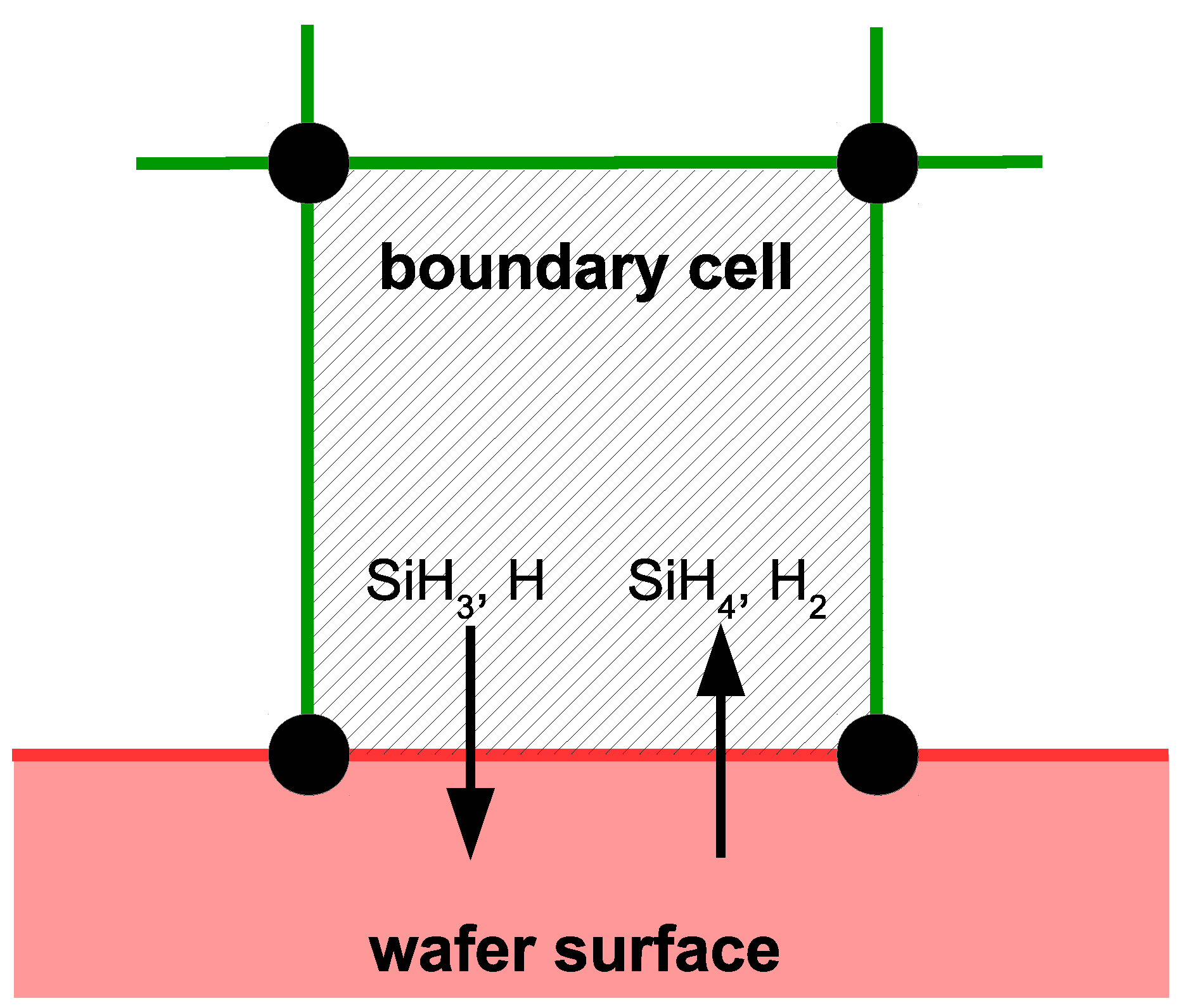
Special consideration must be taken when modeling cells that lie along the surface of the wafer (e.g.,
Figure 5). In addition to the previously detailed transport and reaction phenomena, the cells bordering the surface share mass and energy with the growing thin film layer. Specifically, SiH
and H radicals deposit on the thin film causing a mass sink, while SiH
and H
desorb from the surface representing a mass source. Additionally, energy is consumed and released through the breaking and formation of covalent bonds during the chemisorption process. As a result,
and
terms have been added to the energy and mass balances, respectively. The values of these user defined terms are updated after each time step of the microscopic model to reflect the growth events that have occurred. In the interest of clarity, it is important to note here that microscopic simulations are not conducted within every boundary cell. Instead, microscopic simulations occur at discrete locations across the wafer surface (e.g., ten discrete locations from
r = 0.0 to 10.0 cm are used in this work), and the appropriate mass and energy consumption for the remaining boundary cells are found via linear interpolation. After each boundary cell has been resolved, calculation of the next time step can commence.
2.2.1. Electron Density Profile
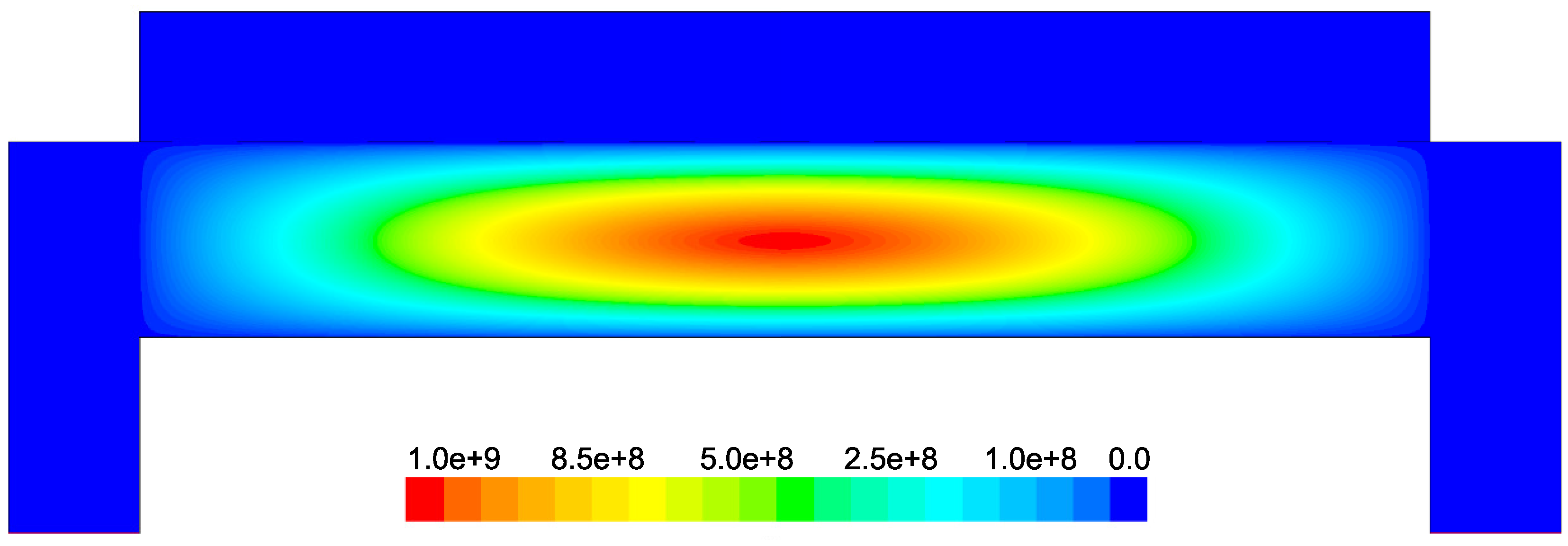
The first nine reactions in
Table 1 involve the creation of radicals via collision with free electrons; therefore, the second user defined function which is key to the accuracy of the plasma phase, is that which accounts for the electron density profile. For plasmas propagating within cylindrical geometries, the electron density can accurately be modeled by the product of the zero order Bessel function and a sine function whose period is twice the parallel plate spacing [
19]. This is described by the following equation:
where
is the maximum electron density,
is the zero order Bessel function of the first kind,
is the radius of the reactor, and
D is the distance between the showerhead and wafer (i.e., the parallel plate spacing). When applied to the PECVD geometry discussed previously, the resulting electron distribution can be seen in
Figure 6. The electron cloud is bounded by the charged region between the parallel plates and demonstrates a maximum, as expected, in the center of the reactor.
2.3. Surface Microstructure Model
The final UDF utilized in the multiscale model is of the greatest complexity as it is responsible for computation of the microscopic domain in its entirety (i.e., the hybrid kinetic Monte Carlo algorithm and communication between boundary cells). Details of the microscopic surface model are presented here in an abbreviated form; however, since simulation results can vary widely based on minor discrepancies in physical phenomena and model parameters, an in-depth discussion of kinetic Monte Carlo processes and complex surface interaction models can be found in the earlier works of Crose et. al [
7] and Tsalikis et al. [
23]. The following subsection provides a brief introduction to the chemistry involved in amorphous silicon deposition as a foundation for the 2D triangular lattice approximation presented later in this work.
2.3.1. Thin Film Growth Chemistry
Throughout this work, deposition within the microscopic model excludes higher order species and aggregates as Perrin et al. [
24] and Robertson [
25] have verified experimentally that >98% of deposition can be attributed to SiH
and H radicals alone. In the neighborhood of the parameter space of interest, namely
T = 475 K and
P = 1 Torr, all other species remain trapped within the macroscopic gas-phase model. As such, the surface interactions for the microscopic domain can be described by the following chemistry.
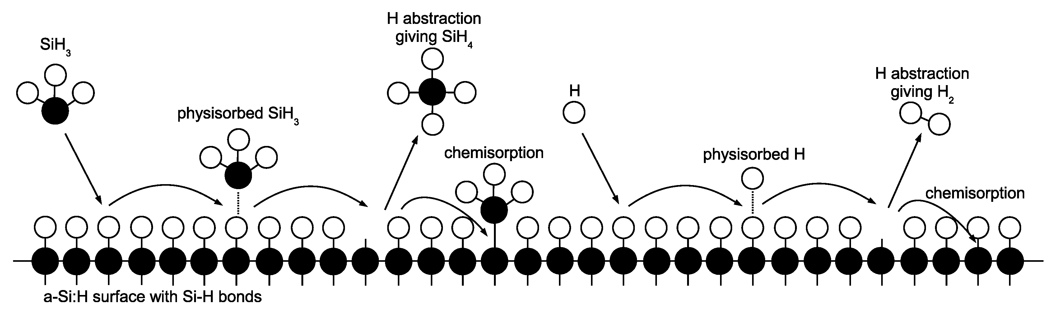
Upon striking the surface of the growing
a-Si:H layer, physisorption occurs as SiH
and H radicals contact hydrogenated silicon sites (
Si–H) according to the following reaction set:
Once a weak hydrogen bond has been formed, rapid diffusion of physisorbed radicals across the lattice surface defines migration events:
The termination of a given migration path falls into one of two categories: hydrogen abstraction,
whereby a physisorbed radical removes a surface hydrogen reforming the stable species (SiH
or H
) and creating a dangling bond (
Si
) in the process, or chemisorption at a preexisting dangling bond site according to the following reactions:
Growth of the lattice proceeds unit by unit via chemisorption of SiH
at dangling bond sites (i.e., the Si atom forms a covalent bond, permanently fixing its location within the amorphous structure). Conversely, chemisorption of H only results in a return of the surface to its original, hydrogenated state. A simplified illustration of the surface chemistry can be seen in
Figure 7.
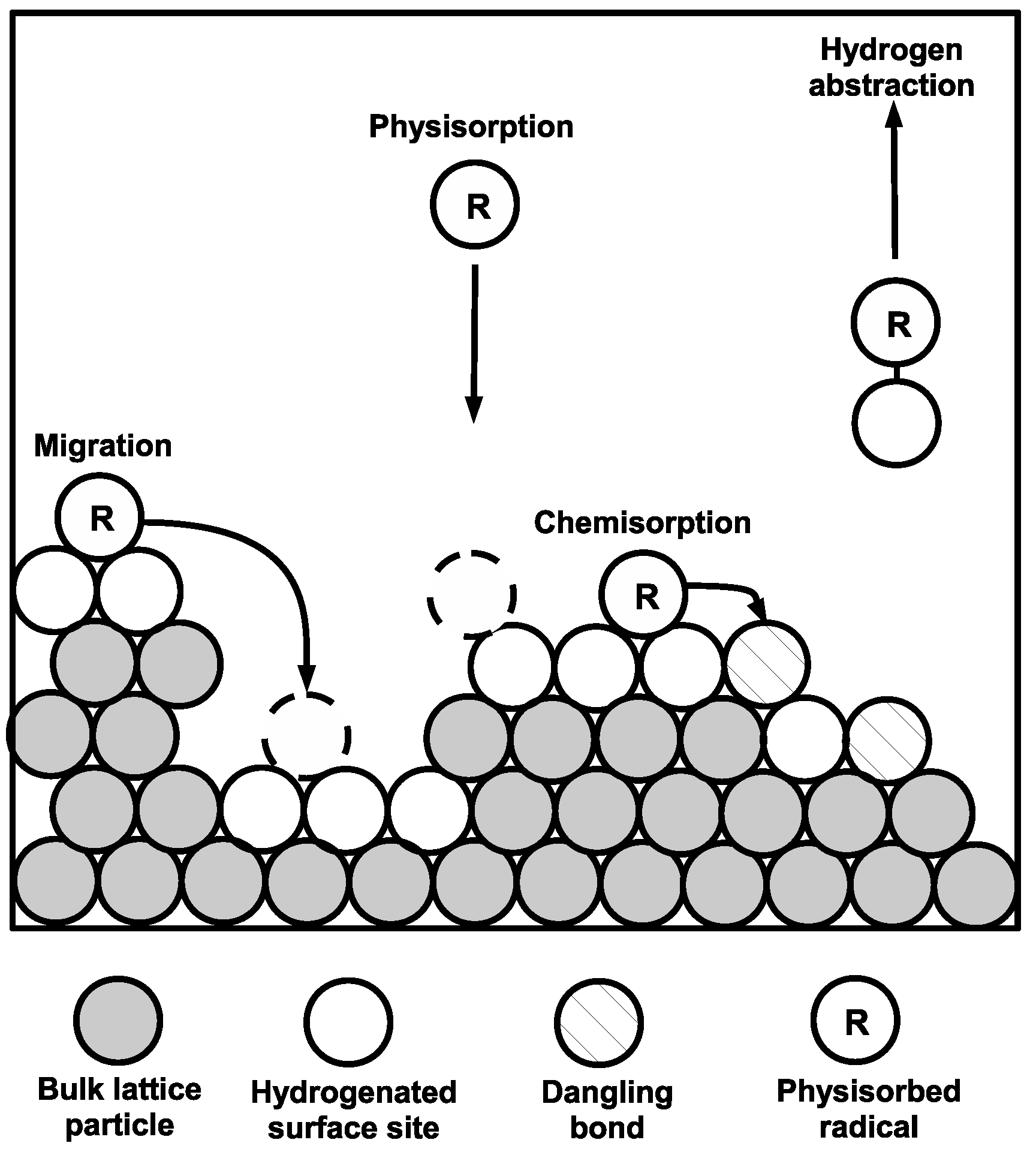
2.3.2. Lattice Characterization
In our recent works [
7,
18], two typical lattice implementations have been explored. The first, a solid-on-solid (SOS) lattice, is composed of a simple square structure in which particles in each successive monolayer are centered directly above those that define the previous layer. Thus, no vacancies are permitted within the bulk of the lattice. Alternatively, the lattice was given a two-dimensional triangular framework without the restriction of SOS behavior. Specifically, adjacent layers form close-packed groups which allow for the creation of porous structure within the growing film. By enforcing a minimum of two nearest neighbors per particle, overhangs may develop which in turn lead to voids in the triangular lattice. This effect can be seen in the 2D triangular surface representation of
Figure 8. Given that experimentally grown
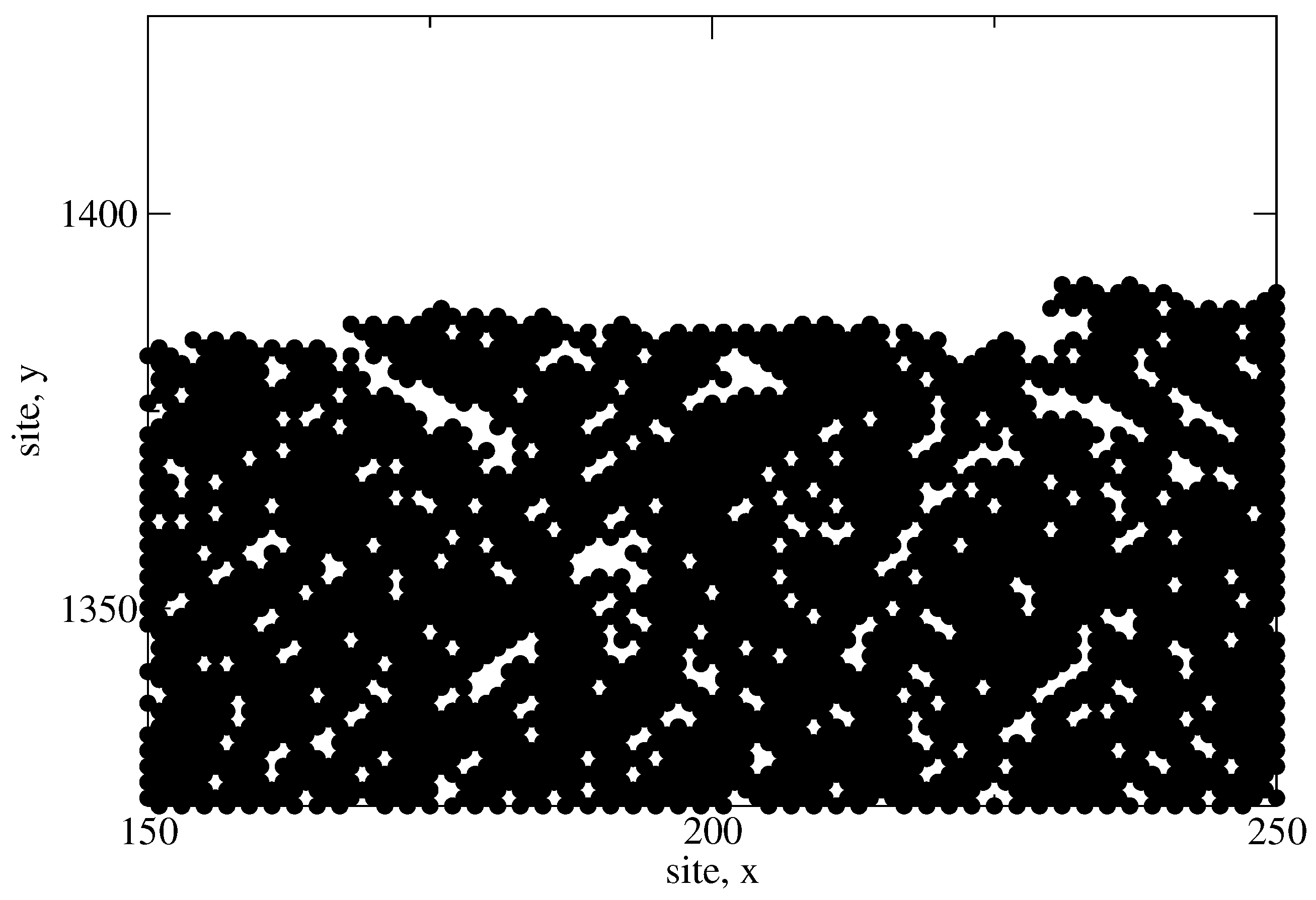
a-Si:H layers have been observed to have void fractions in the range of 10%–20%, the triangular lattice allows for the development of a more representative microscopic model, and is therefore used throughout the remainder of this work.
For each individual microscopic simulation (i.e., for each location along the radius of the wafer), the size of the two-dimensional lattice can be characterized by the product of the length and thickness. The number of lateral sites is denoted by
L and is proportional to the physical length by 0.25
, given a hard-sphere silicon diameter of ∼0.25 nm. The thickness can be calculated from the number of monolayers,
H, using the following equation:
where the factor
accounts for the reduction in thickness due to the offset monolayers which result from the close-packed, hard-sphere structure defined by the triangular lattice (refer to
Figure 8 and
Figure 9). Throughout this work, the number of lateral sites remains fixed at
L = 1200 in order to provide a lattice with enough area for the morphology of the
a-Si:H thin film to be adequately captured without being so large as to pose additional computational challenges and to necessitate the inclusion of spatial variations within the microscopic model. In other words, while significant gradients exist in the concentration of SiH
and H within the PECVD reactor, finite microscopic zones of length ∼300 nm can be assumed to experience uniform deposition rates without the need for spatial considerations.
2.3.3. Relative Rates Formulation
Migration and hydrogen abstraction involve species which exist on the surface of the thin film; as a result, these reactions are thermally activated events and follow a standard Arrhenius-type formulation:
where
is the attempt frequency prefactor (s
) and
is the activation energy of radical
i. Frequency prefactor and activation energy values are drawn from Bakos et al. [
26,
27] to correspond to the growth of
a-Si:H films via the two species deposition of SiH
and H.
Physisorption events originate within the gas-phase and can be described by an athermal or barrierless reaction model based on the fundamental kinetic theory of gases which yields the following rate equation:
where
J is the flux of gas-phase radicals,
is the local sticking coefficient (i.e., the probability that a particle which strikes the surface will ‘stick’ rather than bouncing off),
is the Avogadro number, and
σ is the average area per surface site. Equations (
15)–(
17) can be used to calculate the flux,
J:
where
is the number density of radical
i (here the reactive gas-phase is assumed to be ideal),
is the mean radical velocity,
is the partial pressure of
i,
R the gas constant,
T is the temperature,
is the Boltzmann constant, and
is the molecular weight of radical
i. By substitution of the expression for
J into Equation (
14), the overall reaction rate for an athermal radical
i becomes:
2.3.4. Kinetic Monte Carlo Implementation
Evolution of the lattice microstructure is achieved using a hybrid n-fold kinetic Monte Carlo algorithm for which the overall reaction rate is defined by
where
is the rate of physisorption of SiH
,
is the rate of physisorption of H, and
is the rate of hydrogen abstraction forming SiH
(note: the subscripts
a and
t denote athermal and thermally activated reactions, respectively). In the interest of computational efficiency, surface migration is decoupled and does not contribute to the overall rate. The details and motivations behind decoupling migration events will be discussed at length in the next subsection.
Each kMC cycle begins through generating a uniform random number,
. If
then an SiH
physisorption event is executed. If
then a hydrogen radical is physisorbed. Lastly, if
then a surface hydrogen is abstracted via SiH
.
Physisorption events for each radical type, SiH
or H, proceed through selecting a random site on the surface of the lattice from a list of candidate sites. Acceptable candidate sites are limited to those which exist in either their original, hydrogenated state, or which contain a dangling bond; sites which currently host a physisorbed radical cannot accept additional physisorption events. If the chosen site contains a dangling bond, the particle is instantaneously chemisorbed causing the lattice to grow by one. Hydrogen abstraction occurs by selecting a random SiH
particle from the surface of the lattice and returning it to the gas-phase as the stable species, SiH
. In other words, a migrating SiH
radical removes a hydrogen atom from the surface of the film leaving behind a dangling bond in its place. A second random number,
is now drawn in order to calculate the time required for the completed kMC event:
where
is a uniform random number.
Deposition and movement of particles on the triangular lattice are also governed by what’s known as surface relaxation whereby a minimum of two nearest neighbors is enforced in order to consider a particle location as stable. As an example, if a radical were to physisorb at location (A) in
Figure 9, it would first have to relax to position (C) such that it fits into the predetermined triangular lattice structure. However, at position (C) the incident particle has only a single nearest neighbor and is therefore only quasi-stable. Full stability is achieved by the particle further relaxing to position (D), at which point execution of the kMC algorithm can continue.
2.3.5. Decoupling Surface Migration
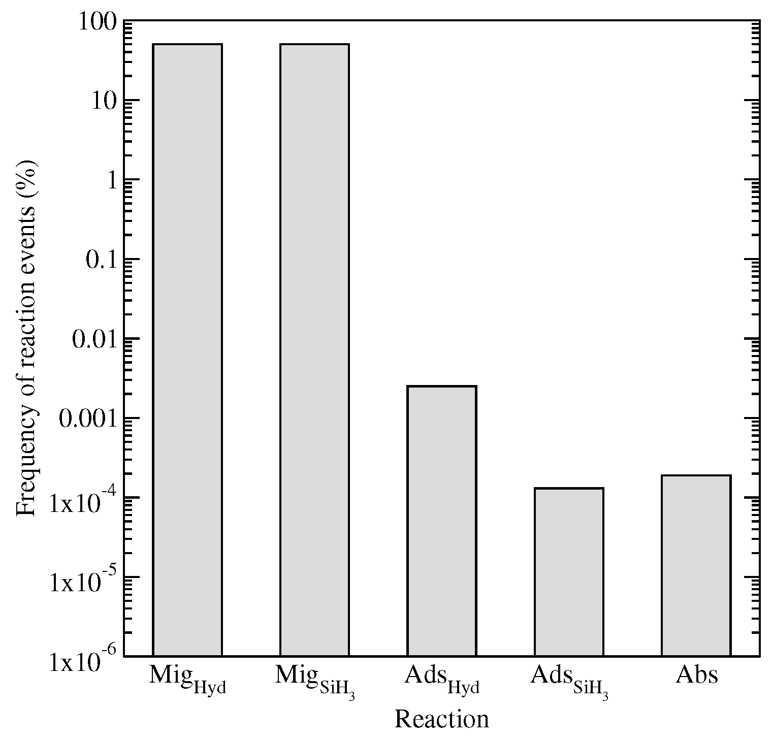
The frequency of reaction events listed in
Figure 10 motivate the choice to decouple migration from other kMC event types. Brute force kMC methods (in which all event types are available for execution) require more than
of computational resources to be spent on migration alone (note: the results in
Figure 10 are typical for
a-Si:H systems operating near
T = 475 K and
P = 1 Torr). Consequently, only a small fraction of simulation time contributes to events leading to film growth while the vast majority is spent on updating the locations of rapidly moving particles. In an effort to reduce the computational demands of the microscopic model, a Markovian random-walk process has been introduced which decouples particle migration from the standard kMC algorithm.
A kMC cycle is typically defined by the execution of single event which moves forward the physical time of the system. In this work the completion of each cycle involves two steps: first, a kMC event is executed according to the relative rates of
,
and
, second a propagator is introduced to monitor the motion of physisorbed radicals. The total number of propagation steps is
+
where
and
and
are the thermally activated migration rates of hydrogen and silane radicals, respectively. Each set of propagation steps,
and
, are split evenly among the current number of physisorbed radicals,
and
. The radicals then initiate a two-dimensional random walk process according to the number of assigned propagation steps. Thus, the intricate movements of an individual particle are approximated via the bulk motion of the propagator. For clarity, the procedure of the random walk process is as follows: a radical type is chosen, a random physisorbed radical of the given type is selected, the weighted random walk with
propagation steps begins, propagation continues until either
steps have occurred or the radical becomes chemisorbed at a dangling bond site, the final position of the propagator is then stored as the radical’s new position and this cycle continues for all
+
physisorbed species. The weighting of each propagation step is designed such that the probability for a particle to relax down the lattice is exponentially higher than jumping up lattice positions (i.e., migration down the lattice is favored). Thus, relaxation and particle tracking are only required to be updated once per particle rather than after each individual particle movement as in brute force methods. In much the same way as physisorption and hydrogen abstraction, the time required for an individual migration step is calculated via the following equations:
Thus, the total time elapsed for all migration events,
, is determined by summation over the number of propagation steps,
Our methodology of decoupling the diffusive processes from the remaining kinetic events has been validated by confirming that the underlying lattice random walk process results: (1) in surface morphologies and film porosities appropriate for the chosen process parameters; and (2) growth rates on par with experimental values. Detailed model validation can be found in the latter half of this paper. It is important to note that film growth continues in this cyclic manner until the kMC algorithm has reached the alloted time step (i.e., until the microscopic model has caught up with the macroscopic, CFD solver). For a more in-depth discussion of the transient operation of the multiscale model, please refer to the following section.
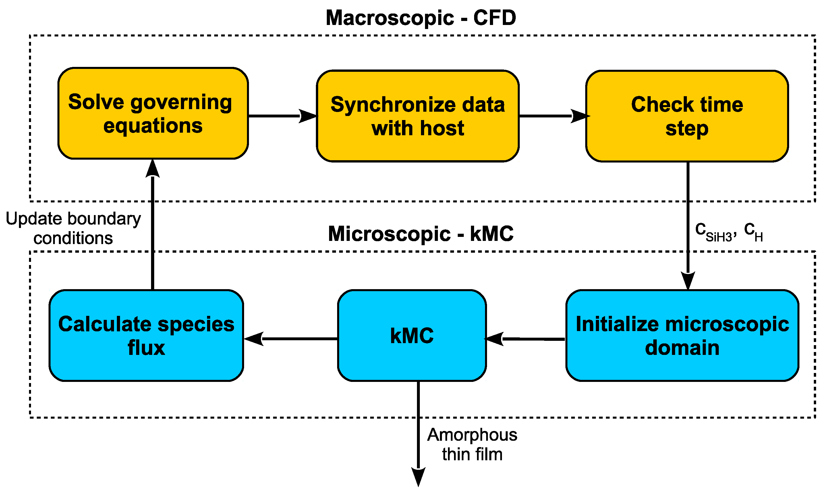
3. Simulation Workflow
At each time step, every cell of the mesh will first solve the governing equations with respect to their reduced spatial coordinates using finite difference methods, then the boundaries along adjacent cells are resolved iteratively. In order to move from one time step to the next, an Implicit Euler scheme is utilized. The result of this method is accurate predictions of the concentrations of each deposition species at all locations within the geometry for a particular time,
t. Given the complete characterization of the plasma for all times, the microscopic model described throughout this work can once again be simulated in parallel such that the resulting thin film layers will be a product of accurate plasma chemistry.
Figure 11 clarifies the proposed multiscale workflow including the communication between domains at each time step.
At a given time, t, the governing equations are solved within each cell of the reactor mesh. The concentrations of the deposition species of interest, SiH and H, are fed to the microscopic domain at which point the kMC model presented earlier can grow the thin film until time t is reached. The boundary cells (i.e., cells which are adjacent to the wafer surface) then receive updated boundary conditions based the the transfer of mass and energy to the microscopic domain. This cycle continues through the completion of the PECVD batch deposition. Please note, the “initialization” of the microscopic domain refers to non-trivial startup costs associated with loading the lattice from the previous cycle (i.e., initialization must be run at every time step).
4. Parallel Computation
Transient operation of the multiscale model presented in this work represents non-trivial computational demands. The simulated deposition of a 300 nm thick a-Si:H thin film alone requires two to three days of computation when using a single processor, and close to a day when utilizing a multi-core personal workstation. Addition of the CFD model increases the computational time of a single batch simulation to greater than a week of continuous processing (thus, for the given system with 120,000 cells in the mesh, the computational demands of the micro- and macroscopic scales are on the same order of magnitude). The results presented in the following sections represent not only the culmination of many test batches during the development of the multiscale model, but also data that has been averaged across several repeated simulations; therefore, serial computation on a single processor corresponds to an impractical task. We present a parallel computation strategy here as a viable solution to mitigate the aforementioned computational demands.
The motivations behind the use of parallel computation are threefold. As mentioned previously, the reduction in simulation time for a serial task is significant through the use of multiple processors. Second, kMC simulations inherently exhibit noise due to the stochastic nature of the model. By repeating a simulation with the same parameters numerous times, we can reduce the noise and obtain more accurate, averaged values. Finally, one might want to perform many simulations at different conditions (e.g., to find suitable model parameters by testing various deposition conditions and calibrating with known experimental data).
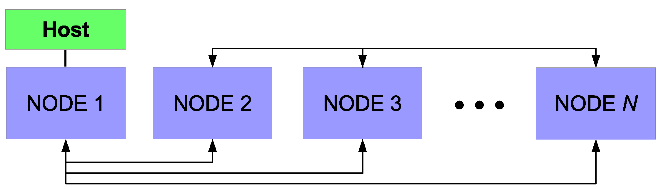
The details of the parallel algorithm and message-passing interface (MPI;
Figure 12) are standard and therefore will not be discussed at this time. The recent publication of Kwon et al. [
28] provides further information on the parallelization strategies on which this work is based; additionally, in-depth studies of parallel processing with applications to microscopic simulations have been made by Nakano et al. and Cheimarios et al. [
29,
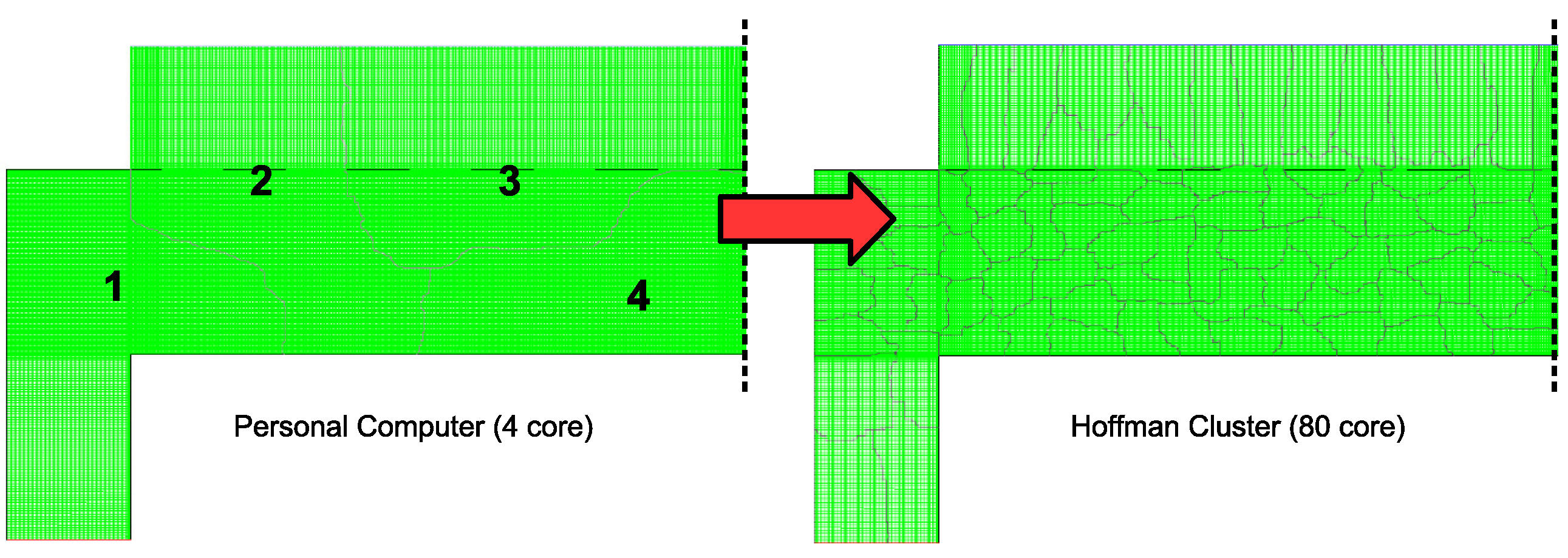
30]. However, as a brief outline, the process of creating a parallel program can be understood through three elementary steps: (1) the original serial task is decomposed into small computational elements; (2) tasks are then distributed across multiple processors; and (3) communication between processors is orchestrated at the completion of each time step. Here decomposition of the serial program is achieved through two separate mechanisms. First, the mesh that defines the 2D axisymmetric geometry can be discretized into a number of smaller mesh regions (see
Figure 13) in which a reduced number of cells reside. For example, in the case of a typical personal computer with 4 cores, each core would be assigned roughly 1/4 of the original 120,000 cell mesh. By utilizing UCLA’s Hoffman2 computation cluster, up to 80 cores are available for parallel operation resulting in each core containing less than 2000 cells. The maximum achievable speedup given the aforementioned parallel programming strategy can be defined by:
where
S is the maximum speedup,
P is the fraction of the program which is available for parallelization (i.e., the fraction of the original serial task which may be discretized), and
N is the number of processors utilized [
31].
In reality, the maximum speedup deviates from this formulation as a second mechanism for decomposition of the serial program must be considered. Although the mesh required for the CFD algorithm can be decomposed as presented above, the microscopic model cannot directly benefit from the parallel programming scheme. Individual thin film simulations (i.e., discrete simulations of 1200 particle regions across the wafer surface) cannot be decomposed into smaller computational elements. Instead, individual microscopic simulations are assigned to the processor in which the adjacent mesh region is contained. In other words, if the cells bordering the wafer surface are contained within processor n, thin film growth for that region is computed on processor n for each time step. At the completion of a time step, each node must resolve its boundaries with neighboring nodes via communication through the host processor before computation of the multiscale model can continue.
5. Steady-State Behavior
Before the results of the multiscale CFD model can be discussed, we must first validate each domain with available experimental data. To that end, a number of batch simulations have been conducted using an inlet gas composition, reactor temperature and pressure chosen to represent industrially relevant PECVD conditions. Namely, the inlet gas is composed of a 9:1 mixture of hydrogen to silane, the parallel plates are maintained at T = 475 K and a chamber pressure of P = 1 Torr is used. In the following section three criteria have been evaluated in order to determine the fidelity of the proposed model to experimentally grown a-Si:H thin films. It is important to note that although the results presented in the following sections have been collected after the reactor has reached steady-state, the multiscale model maintains transient operation. Startup of the PECVD reactor may affect the hydrogen content and porosity of the thin film layer, and therefore cannot be excluded.
5.1. Plasma Composition, Porosity and Hydrogen Content
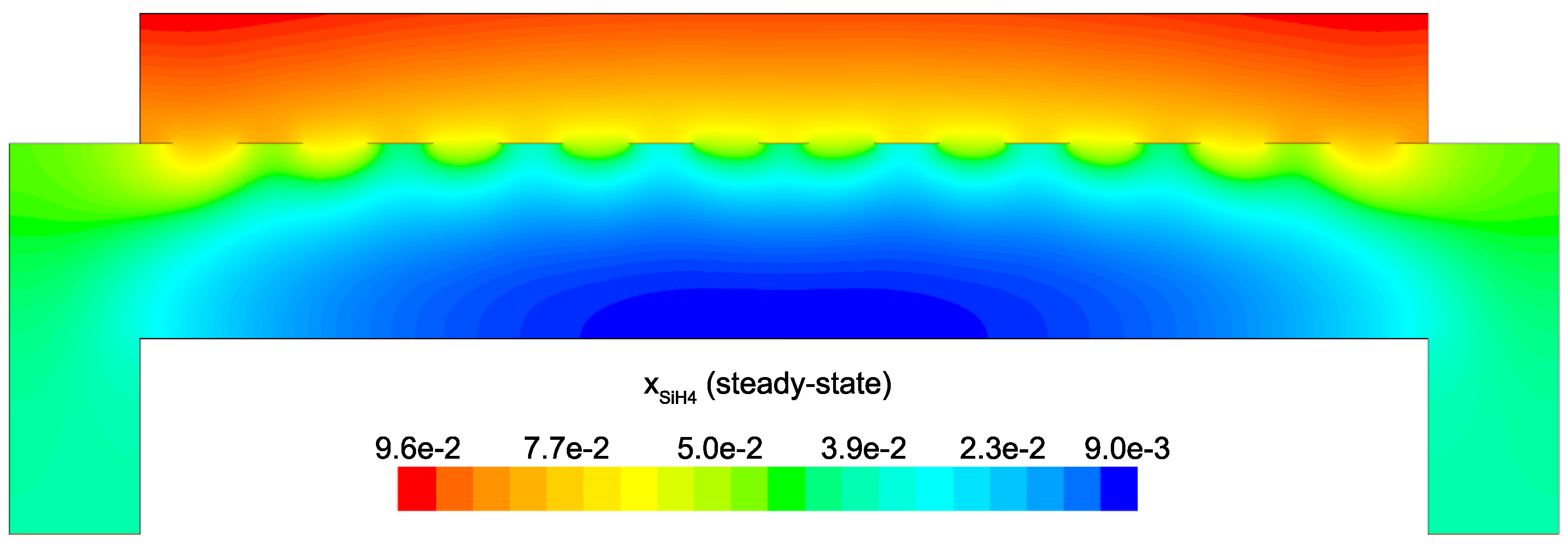
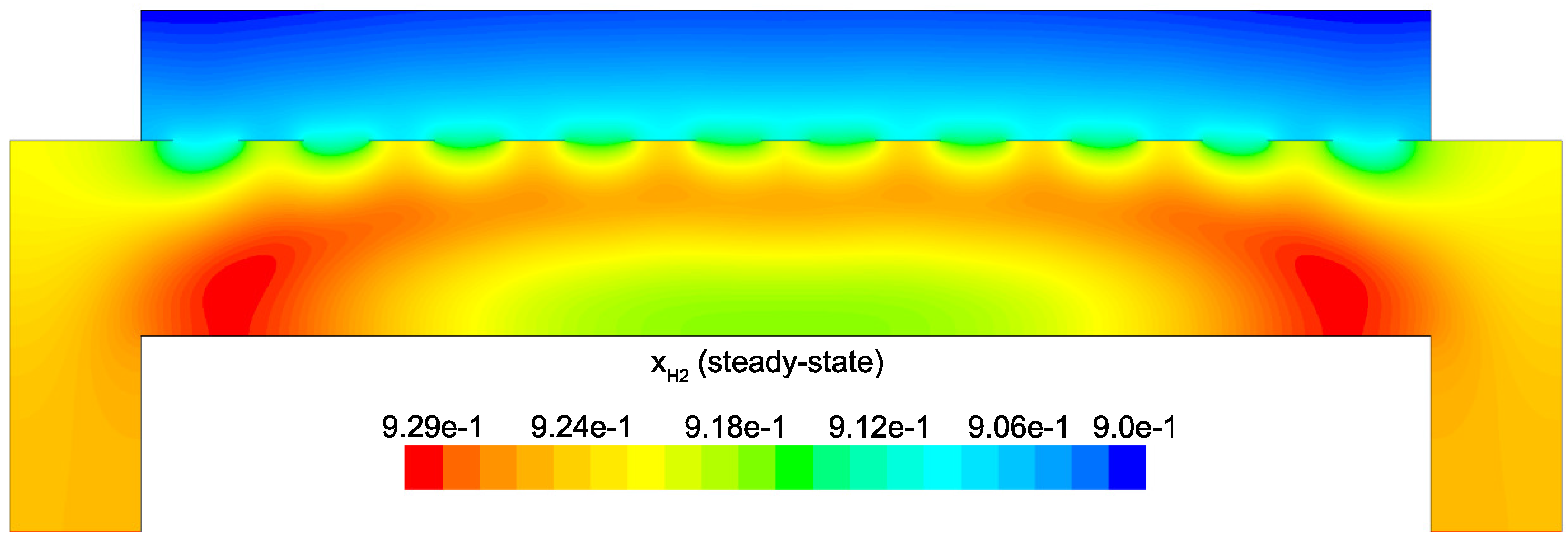
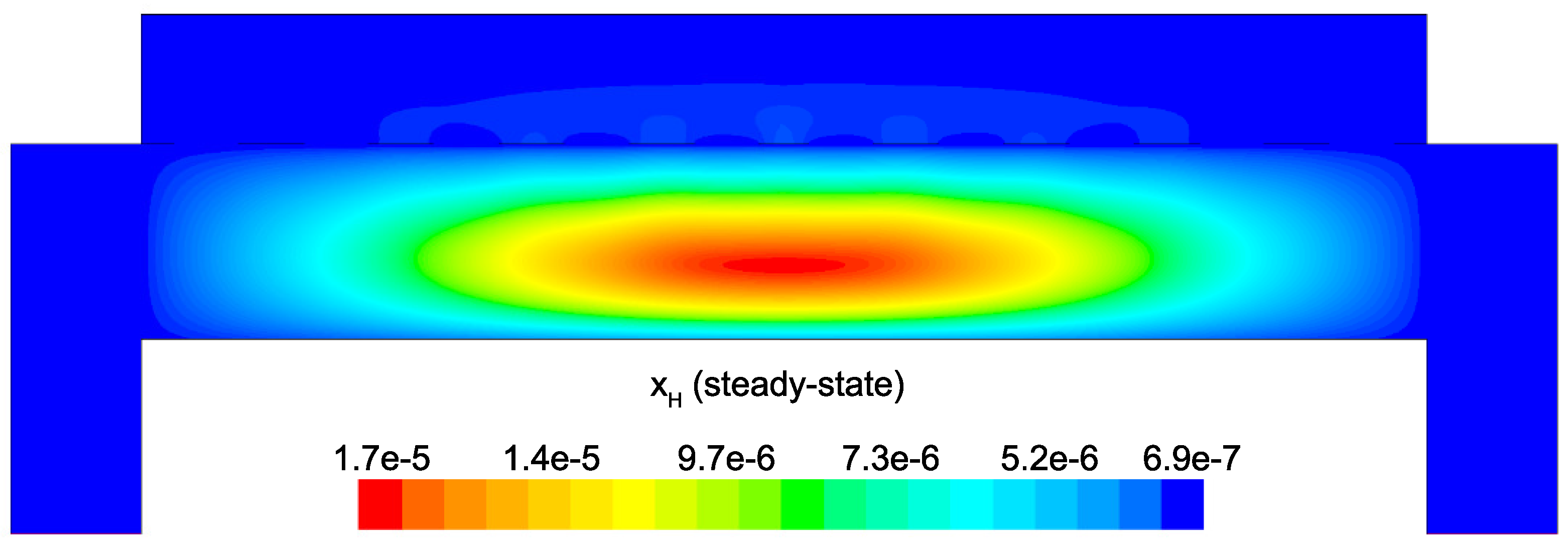
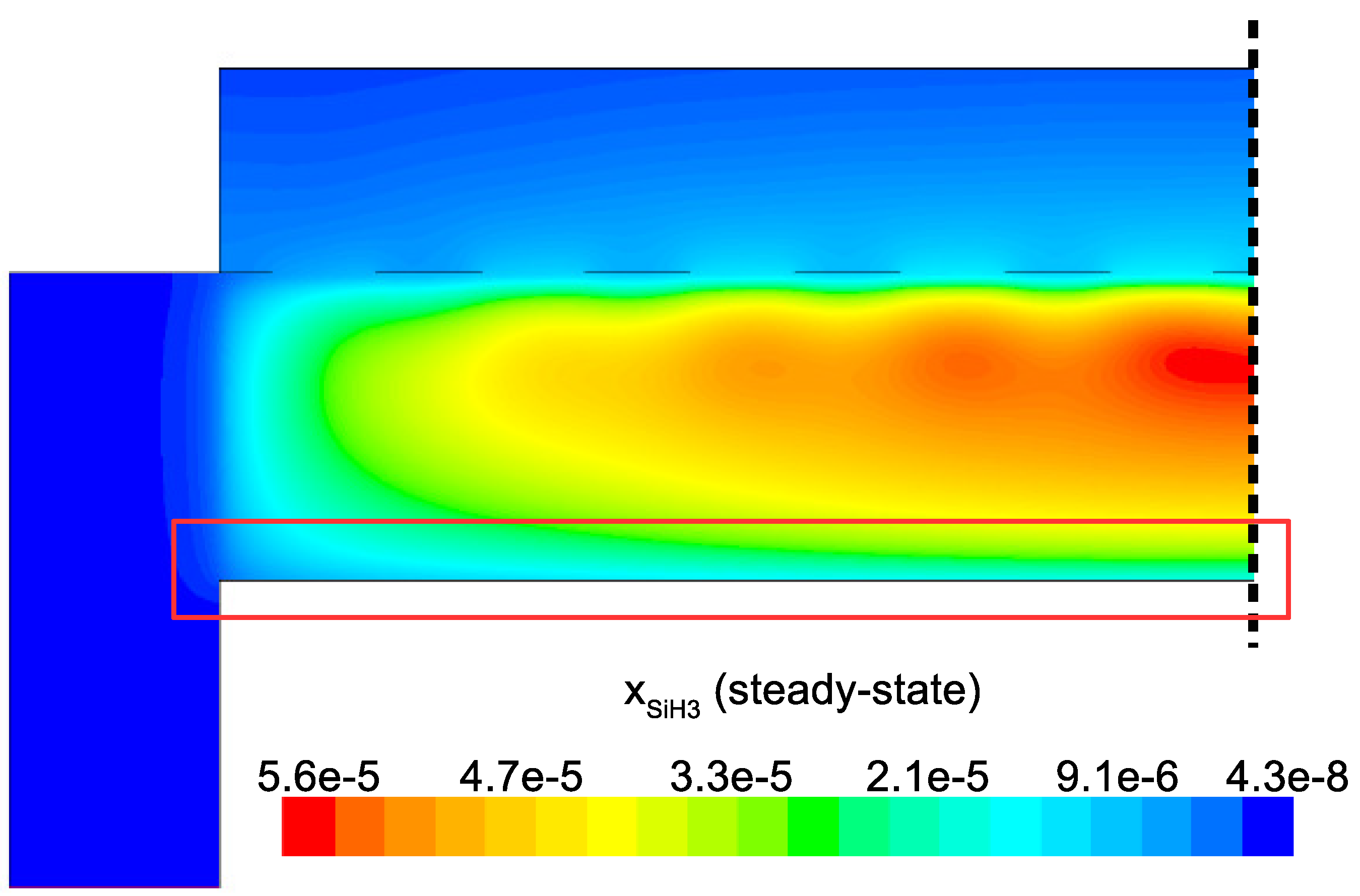
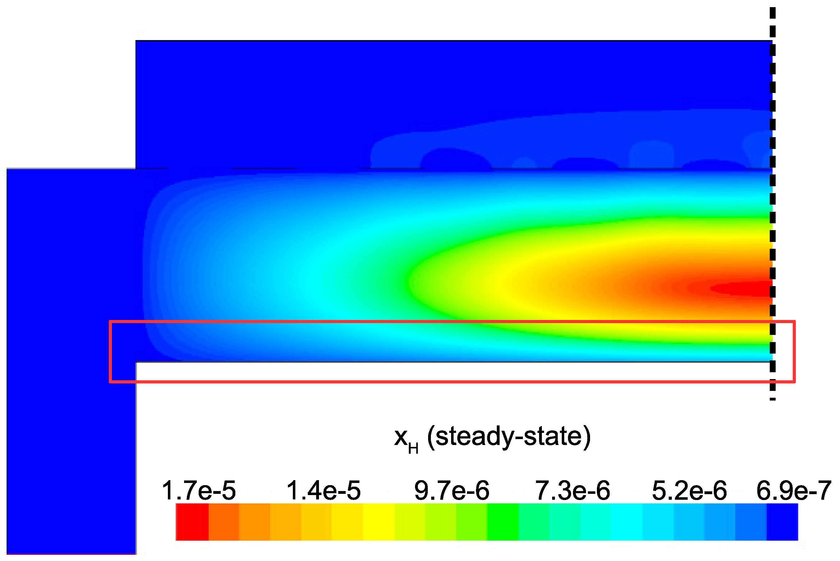
Figure 14 and
Figure 15 detail the distribution of the process gases within the PECVD reactor at steady-state. As one might expect, before reaching the showerhead holes, both SiH
and H
appear in similar concentrations to the inlet gas. Once entering the plasma region the silane gas is quickly consumed and continues to decrease in concentration towards the surface of the wafer. Due to the reaction set presented previously, the behavior of H
within the plasma is more complex. Hydrogen is primarily a product of the dominant gas-phase reactions (see
Table 1), and this effect is reflected in the maximum concentration occurring near the outlets of the chamber.
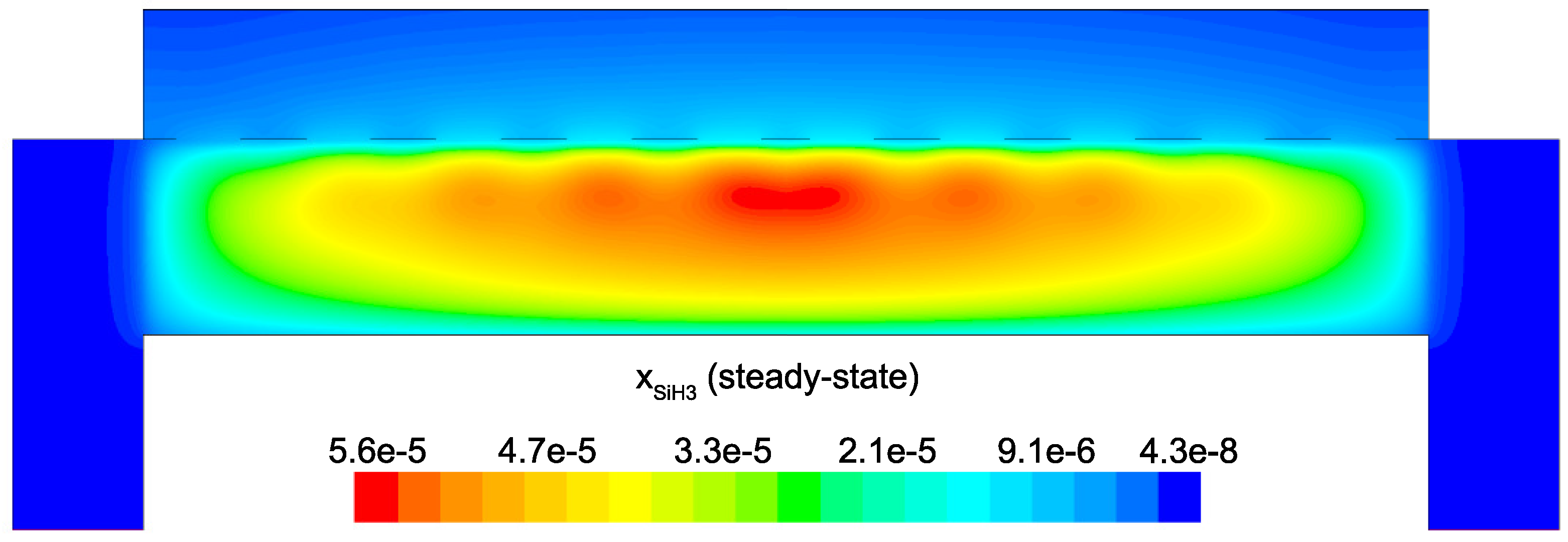
Since growth of the thin film is dependent on the concentration and distribution of SiH
and H within the reactor, the steady-state profiles of these two species are of particular importance. Silane radicals (SiH
) are observed to have a maximum mole fraction at the center of the PECVD reactor with significant gradients in both the
r and
z directions. Specifically,
Figure 16 and
Figure 17 demonstrate that the concentration of the deposition species track closely with the electron density (recall,
Figure 6). Due to the relatively short lifespan of radicals within a plasma, it is reasonable that the concentration of SiH
and H will be tied to the distribution of electrons rather than to convective and diffusive effects. Additionally, consumption of radicals during the growth of the thin film would suggest that depleted concentrations would be observed near the wafer surface; as expected, regardless of radial position, at
z = 0 (along the wafer surface) a boundary layer can be clearly seen in
and
. Similar behavior has been predicted for the dominant deposition species in the detailed work of Amanatides et al. [
32] and Kushner, M. [
22], which yields confidence in the plasma composition obtained here.
The next criteria of interest is the hydrogen content of the thin film as predicted by the microscopic model. In the earlier discussion of the lattice character, the development of porosity within the amorphous structure was highlighted. Hydrogen remains bonded to the interior surfaces of mono- and di-vacancies, as well as within much larger, long range voids.
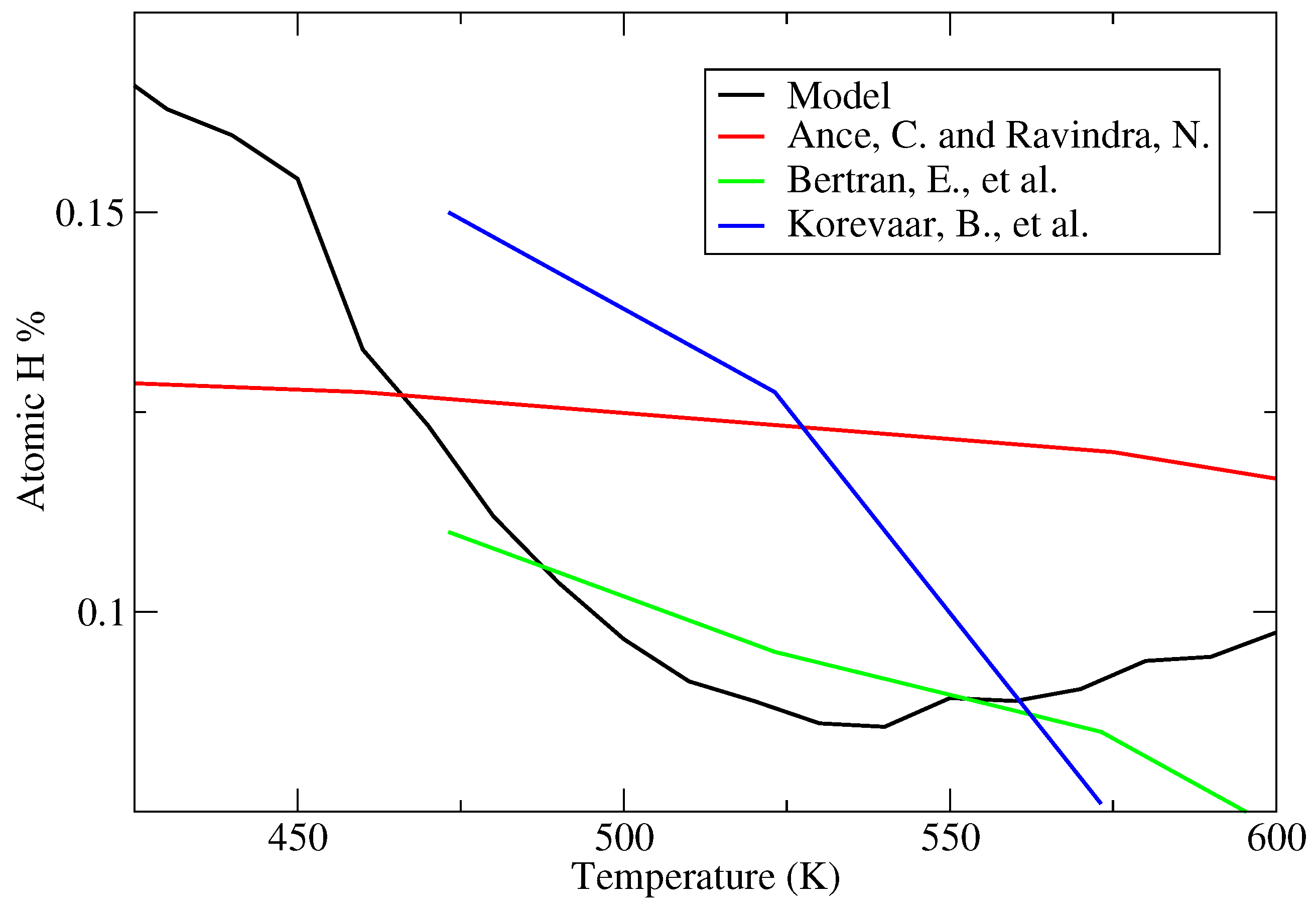
Figure 18 shows a portion of a completed
a-Si:H thin film which demonstrates the porous nature and the various void shapes produced. In an effort to calibrate the hydrogen content with experimentally obtained data, a number of batch PECVD processes are conducted using varying deposition parameters; specifically, the deposition temperature in successive batches is varied which yields thin film layers with different morphologies and degrees of bonded hydrogen. Comparing the recorded values to those reported in literature [
33,
34,
35] reveals three distinct regions of interest: (1) below 500 K the hydrogen content of the
a-Si:H thin film decreases linearly with increasing deposition temperature; (2) between 500 and 575 K atomic hydrogen fractions remain relatively constant (∼9%) and (3) above 575 K the hydrogen capacity of the porous film begins to increase (see
Figure 19). While the observed atomic hydrogen falls within the accepted experimental range regardless of deposition temperature, the gradual upturn of hydrogen fractions above 575 K contradicts the expected behavior. Increasing the temperature of the film allows for more rapid migration of physisorbed species along the surface of the lattice, resulting in a more stable, less porous structure with reduced interior surface area available for hydrogen bonding. Consequently, a linear decrease in atomic hydrogen is observed in all four data sets as the deposition temperature is increased below the 575 K threshold. Deviation in the microscopic model’s behavior above 575 K is believed to be due to competition between surface events. At high temperatures the frequency of hydrogen abstraction continues to grow which allows for premature chemisorption of migrating SiH
radicals. In other words, covalent bonds are formed in unfavorable locations before a more stable, close-packed structure can be achieved. Nonetheless, the operating conditions within this work call for a temperature of 475 K which lies well within the linear region.
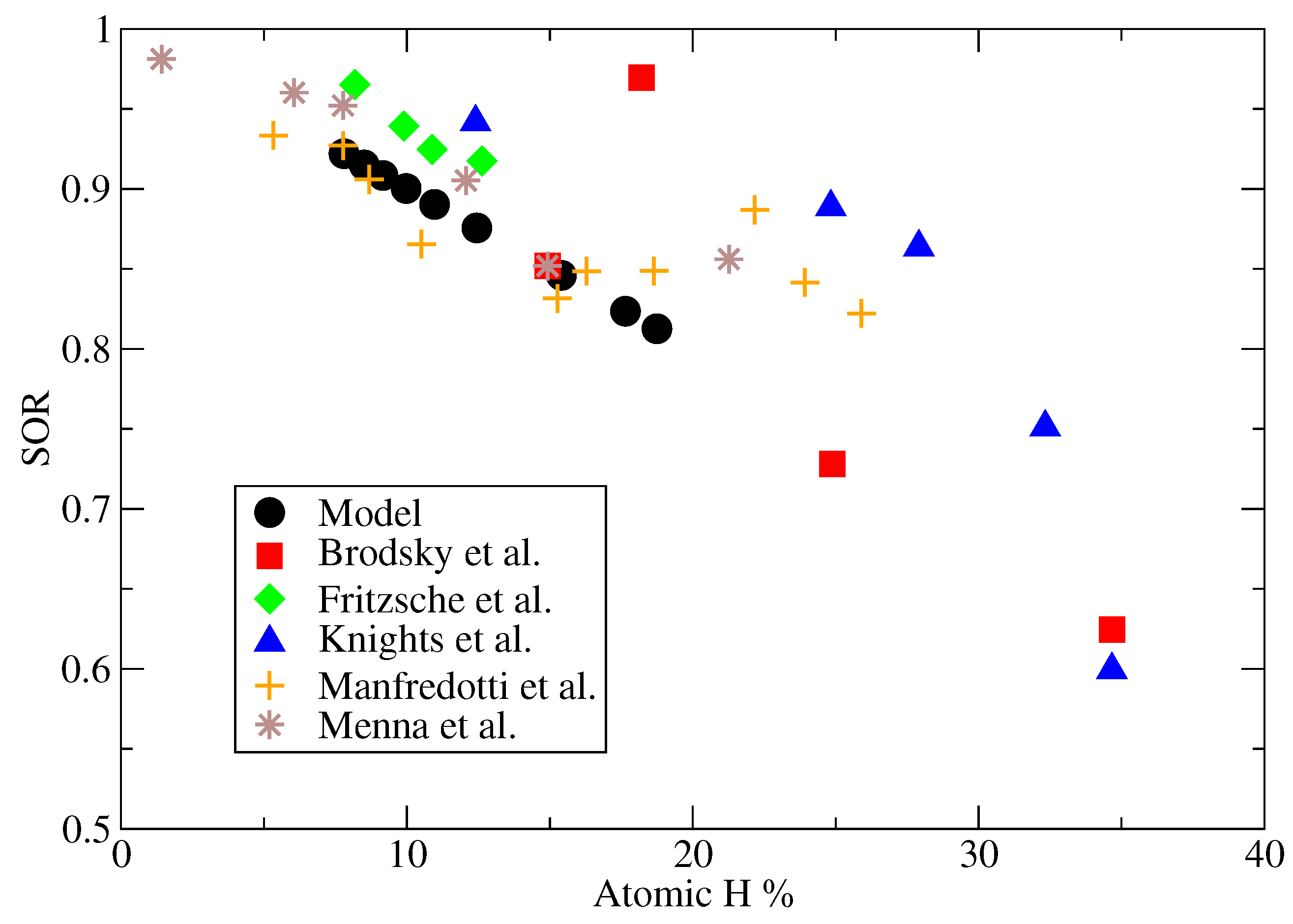
Given the high complexity of the thin film morphology and near limitless distributions of voids which can lead to a specific hydrogen fraction, the validity of the microscopic model cannot be determined from the hydrogen content alone. As an example, two films could be deposited with identical degrees of porosity; the first may have scattered small vacancies while the second could contain a single large pore. While both films maintain the same overall porosity, the amount of bonded hydrogen will vary widely due to differences in interior surface area. As a result, an additional criteria is defined here, the relationship between the porosity of the film and the associated hydrogen content. For consistency with data obtained from literature, the site occupancy ratio (SOR) is used as a measure of porosity:
where
n is the number of occupied lattice sites and
is the total number of sites within the lattice. Again, given that hydrogen persists on the interior surfaces of the film, it is expected that a strong correlation exists between the hydrogen content and SOR which will allow for a more detailed evaluation of the accuracy of the microscopic model.
Another set of batch deposition processes were performed in which the pressure was maintained at
P = 1 Torr and the inlet gas compositions at a 9:1 ratio of hydrogen to silane. The temperature of the wafer was increased incrementally from 450 K to 500 K and at the completion of each batch the SOR and atomic hydrogen fraction was recorded. In
Figure 20, this data has been plotted alongside experimentally grown films obtained from five different literature sources [
36,
37,
38,
39,
40]. As expected from the bonding of hydrogen on the interior surfaces of amorphous silicon films, all six data sets demonstrate a similar trend of increasing hydrogen fractions with decreasing site occupancy ratios. Additionally, regardless of SOR the microscopic model predicts a hydrogen content value consistent with the range observed experimentally. These results yield confidence in the ability of the multiscale model presented here to reproduce thin film layers with not only the correct amount of bonded hydrogen, but also with lattice morphologies with high fidelity to those produced via commercially available PECVD systems.
6. Multiscale CFD Analysis
The primary motivation for the development of a multiscale CFD model for the PECVD of silicon thin films is to explore complex phenomena otherwise unobservable by a macroscopic or microscopic simulation alone. To that end, we now comment on the interconnection between these two domains. Specifically, at the macroscopic scale significant gradients exist in the concentration of the deposition species of interest, SiH
and H. Meaning, microscopic simulations at various points along the surface of the wafer should yield non-uniform thin film character due to receiving spatially varying input parameters from the CFD model. This effect can be readily seen in
Figure 21 and
Figure 22 by narrowing our focus to the region just above the surface of the wafer. As discussed in the steady-state analysis, radial dependence of
and
develops due to consumption of the gas as it flows radially outward through the electron cloud and across the wafer. Given that growth of
a-Si:H films is dependent on SiH
radicals reaching the surface, it is likely that at the completion of a batch, the thickness of the thin film layer will not be uniform (further discussion of thickness non-uniformities can be found in the works of Armaou et al. [
14] and Sansonnens et al. [
16]).
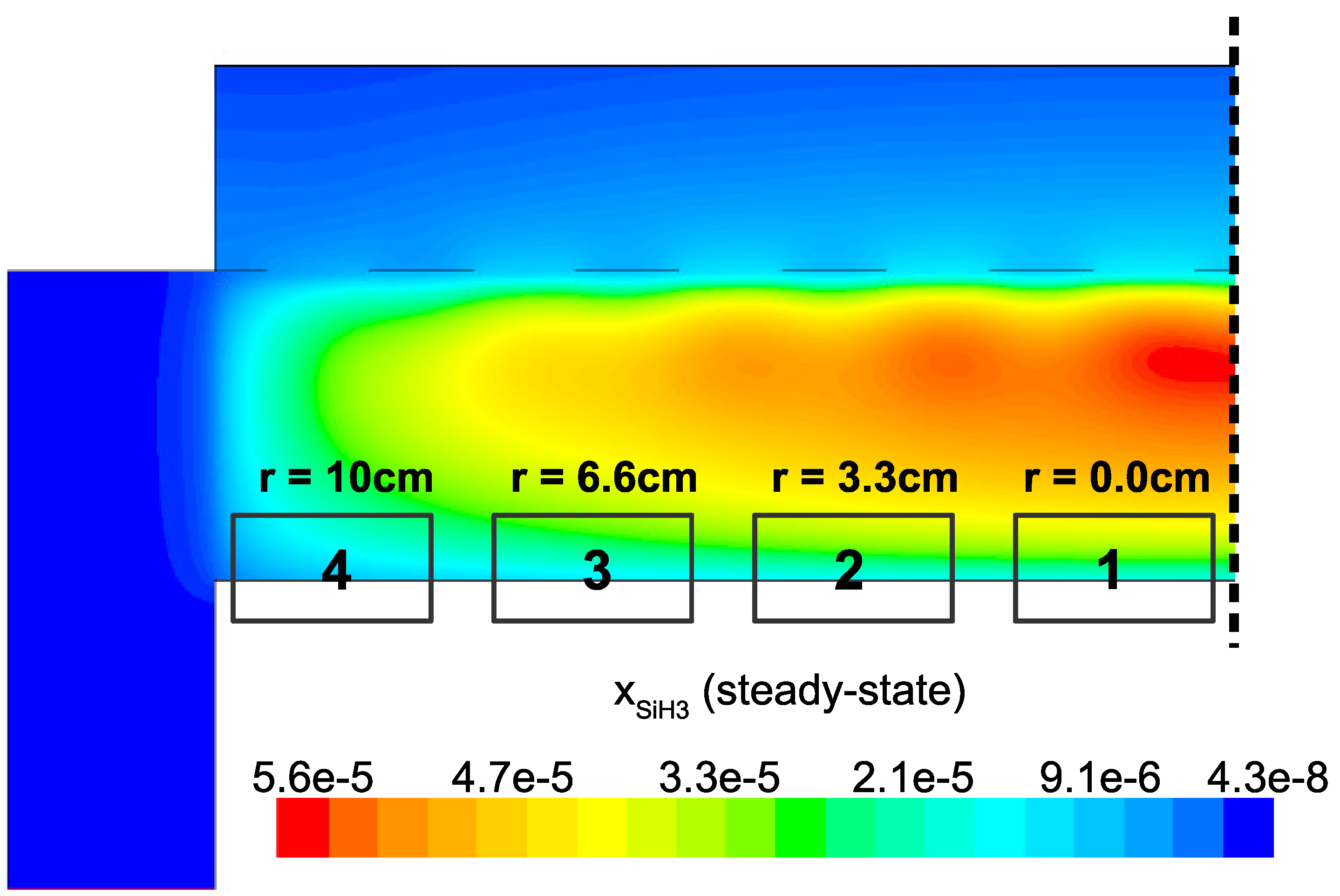
In an effort to quantify the non-uniformities predicted above, four distinct locations across the wafer surface are defined as shown in
Figure 23. During the operation of the multiscale model the output from the microscopic domain at each location is recorded (i.e., thin film samples from
r = 0.0,
r = 3.3,
r = 6.6 and
r = 10 cm are collected). Analysis of each thin film sample may yield insight into the performance of the PECVD reactor as well as the character of the amorphous product.
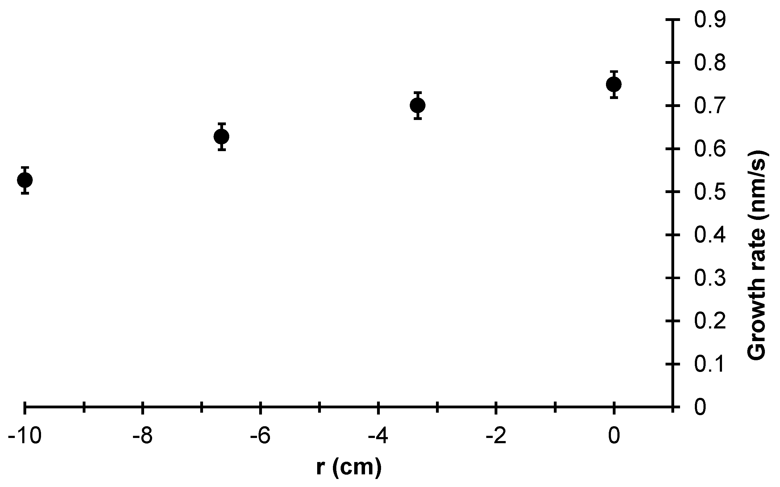
Figure 24 shows the growth rate of the thin film at each radial location averaged over 10 independent batch simulations. A clear dependence on radial position can be seen with >20% difference between the growth rates of the film at
r = 0.0 cm and
r = 10 cm. Given that the goal of PECVD processing of
a-Si:H is to deposit thin films with uniform thickness and photovoltaic properties, a 20% non-uniformity in product thickness represents an unacceptable margin. In terms of photovoltaic properties, Staebler and Wronski [
41] and Smets et al. [
42] have demonstrated that the hydrogen content and porosity of amorphous silicon thin films are tied directly to the efficiency of the solar cell produced. Therefore, the uniformity of bonded hydrogen and porous structure across the film is of great interest.
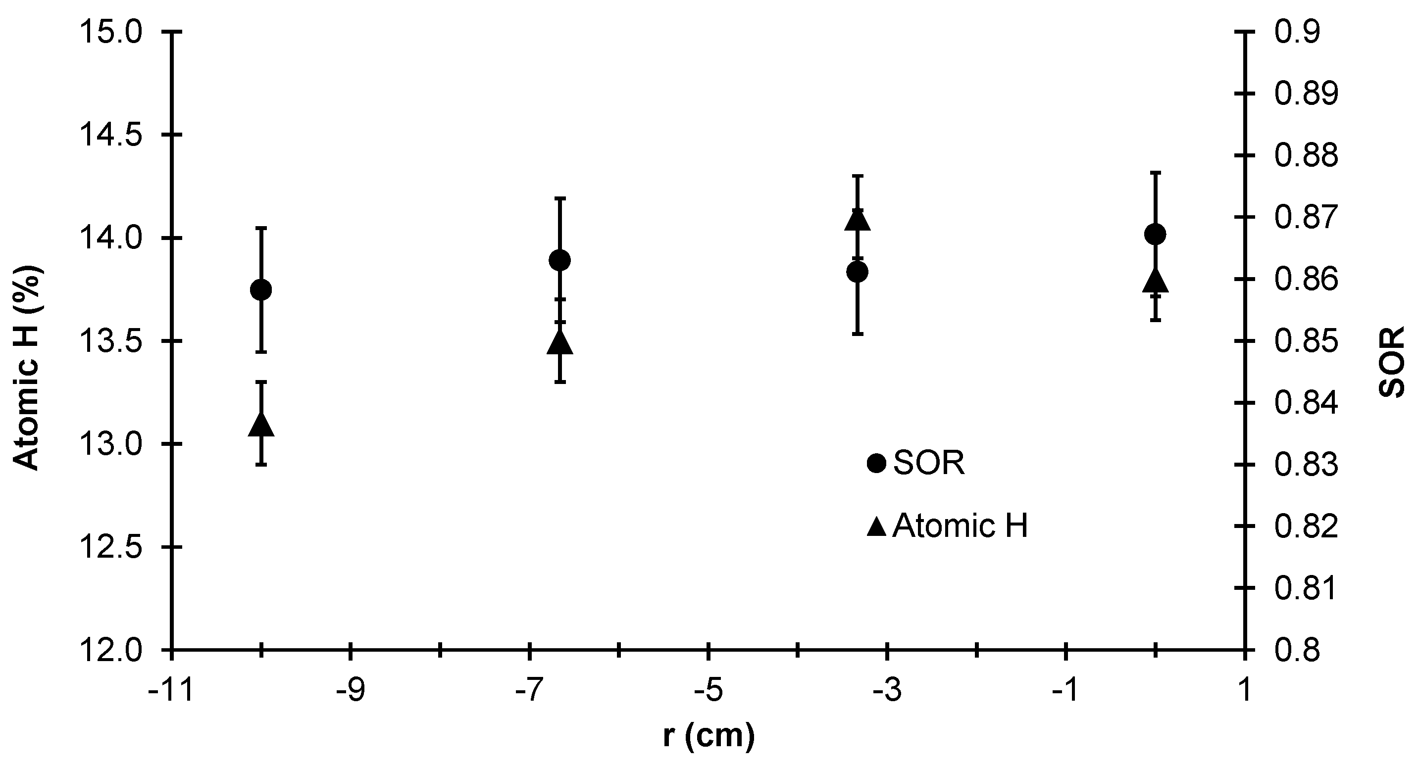
To that end,
Figure 25 lists the SOR and atomic hydrogen % averaged over 10 independent batch simulations for the same four radial locations described previously. The SOR from the center to the edge of the thin film layer remains relatively unchanged (i.e., the difference between each data point lies within the standard deviation of the data set). This is likely due to the fact that all four radial locations experience the same deposition temperature; recall from the earlier discussion of validation criteria that the morphology of the film is dependent on the temperature of the wafer. However, non-trivial differences in the hydrogen content of the film can be seen between
r = 0.0 cm and
r = 10 cm. Due to the significant gradient of
observed in the steady-state concentration profile (see
Figure 22), the radial non-uniformity in the film’s hydrogen content is expected. It is important to note that while the two data sets presented here are unrelated to the thickness non-uniformity, the hydrogen content and SOR remain industrially relevant parameters due to the Staebler-Wronski effect.
The results presented here highlight the importance of accurate reactor modeling; specifically, the importance of utilizing multiscale models which capture the behavior of the reactor as a whole. Information on film non-uniformities obtained via the multiscale PECVD model developed here may provide insight into the design of improved reactor geometries and operational strategies otherwise unavailable using traditional modeling approaches.
7. Conclusions
A multiscale CFD simulation framework, including both a macroscopic CFD model and a microscopic surface interaction model, has been presented here with applications to silicon processing via PECVD. Within the macroscopic domain, mass, momentum and energy balances have been solved by discretization of the PECVD geometry using a 2D axisymmetric mesh and finite difference methods. Along the boundary of the 20 cm diameter wafer, a hybrid kinetic Monte Carlo algorithm has been proposed to account for complex phenomena within the microscopic domain describing thin film growth. A parallel operation strategy has been implemented and demonstrated to reduce the computational demands of the multiscale CFD model and allow for the operation of an otherwise computationally prohibitive model. Together the macroscopic and microscopic simulations have yielded insight into the operation of PECVD systems; specifically, observed non-uniformities in the growth rate (>20%) and hydrogen content of the thin film product suggest that detailed modeling offers the capacity for improved reactor geometries and flow characteristics.


