Article

Fabrication of Efficient Cu2ZnSnS4 Solar Cells by Sputtering Single Stoichiometric Target

1
School of Photovoltaic and Renewable Energy Engineering, University of New South Wales, Sydney 2052, NSW, Australia
2
UCL Institute for Materials Discovery, University College London, London WC1E 7JE, UK
*
Authors to whom correspondence should be addressed.
These authors contributed equally to this work.
Coatings 2017, 7(2), 19; https://doi.org/10.3390/coatings7020019
Submission received: 16 December 2016 / Revised: 6 January 2017 / Accepted: 20 January 2017 / Published: 24 January 2017
(This article belongs to the Special Issue Thin Film Semiconductors for Photovoltaic Applications)

Abstract

:
Low cost single stoichiometric target sputtering of Cu2ZnSnS4 (CZTS) precursor has been adopted to fabricate CZTS solar cells. The effect of a series of deposition pressures and deposition durations on the device performance has been investigated. A 3.74% efficient solar cell has been achieved at a base pressure of 1 × 10⁻⁴ Torr with a stoichiometric target, which to the authors’ knowledge, is the record efficiency for such a stoichiometric target.

1. Introduction

Cu2ZnSnS4 (CZTS) is one of the most promising thin film solar cell absorber candidates owing to its natural earth abundance, direct band gap with the optimal value of 1.45 eV, and its environmentally compatible nature [1,2]. Sputtering is a low cost option for the production of CZTS solar cells due to the large material usage, uniform large area deposition, and the ease of scale-up [3,4]. Single target sputtering is even cost effective due to the lower power supply required and easier control of the precursor deposition in comparison with multi-target sputtering; additionally, it requires less diffusion of elements. Therefore, single target sputtering leads to less voids, better film quality, and higher efficiency compared with the co-sputtering technique [5]. There have already been a few attempts in the literature that generally use Cu poor Zn rich targets [4,5,6]. The highest efficiency of a single target sputtering CZTS solar cell is 6.48%, with a target composition of Cu:Zn:Sn = 1.68:1.1:1 and sulfurization in a H2S atmosphere which has proven to be superior to S powder sulfurization [5,6]. However, for a stoichiometric CZTS target, no efficiency has been reported yet [5,6]. This paper uses a stoichiometric CZTS target to reduce the secondary phases and maintain the single phase in the target, because CZTS has a very narrow single phase composition region [7]. S powder was adopted for sulfurization because it is a relatively low cost option.

2. Materials and Methods

The Mo coated soda lime glass substrate has a sheet resistance of 0.15 Ω/□. The CZTS precursors were sputtered onto the substrates using a stoichiometric compound target in a single target sputter chamber. The target was directly facing down the substrate with a shutter in the middle and the distance between the substrate and target was 10 cm. The sputter target cleaning was conducted for 5 min prior to precursor deposition, after which the pressure reached a base pressure of 1 × 10⁻⁴ Torr with the shutter in the closed position. The shutter was then switched to the open position to allow precursor deposition onto the substrate. A series of deposition pressures and deposition durations were investigated: 5 mTorr for 30 min, 7.5 mTorr for 60 min, 10 mTorr for 30 min and 60 min, and 12.5 mTorr for 60 min. The deposition pressure was adjusted by a throttle valve. The Ar flow rates were kept at 10 standard cubic centimeter per minute (sccm) for target cleaning and precursor deposition. All the precursors were then sulfurized in a dual zone tube furnace OTF-1200 MTI (MTI Corporation, Richmond, VA, USA) at 570 °C in a sulphur (S) atmosphere for 30 min with the S zone temperature held at 250 °C, which was vacuumed to 400 Torr with the two ends of the tube furnace sealed according to the procedure in [8]. The annealed samples were then subject to chemical bath deposition of CdS, and then sputtering deposition of intrinsic ZnO (i-ZO) and Al doped ZnO (AZO) sequentially, the details of which are in [9]. A conductive Ag glue was then pasted on the window layer as the top electrode and the cell area was defined by mechanical scribing to be 0.5 cm2. Details can be found in [10].
The SEM images were captured using a FEI Nova NanoSEM230 system (FEI Corporation, Hillsboro, MA, USA) equipped with an energy dispersive spectroscopy (EDS) detector for chemical composition measurements as well. PANalytical’s X’Pert Pro materials research diffraction system (Panalytical, Almelo, The Netherlands) was used for XRD measurements of crystal structural quality of the CZTS films. A Renishaw inVia spectrometer (Renishaw plc, Gloucestershire, UK) was used to conduct Raman measurements with a 514 nm laser excitation. The QEX10 system (PV MEASUREMENTS Inc, Boulder, CO, USA) was utilised for external quantum efficiency (EQE) measurements. A Perkin Elmer Lambda 1050 spectrophotometer with an integrating sphere (IS) (Perkin Elmer, Singapore, Singapore) was used to measure the hemispherical reflectance (R) of the CZTS films. Light IV measurement was performed at 25 °C under AM 1.5 G illumination with the JSC calibrated by EQE measurement.

3. Results and Discussion

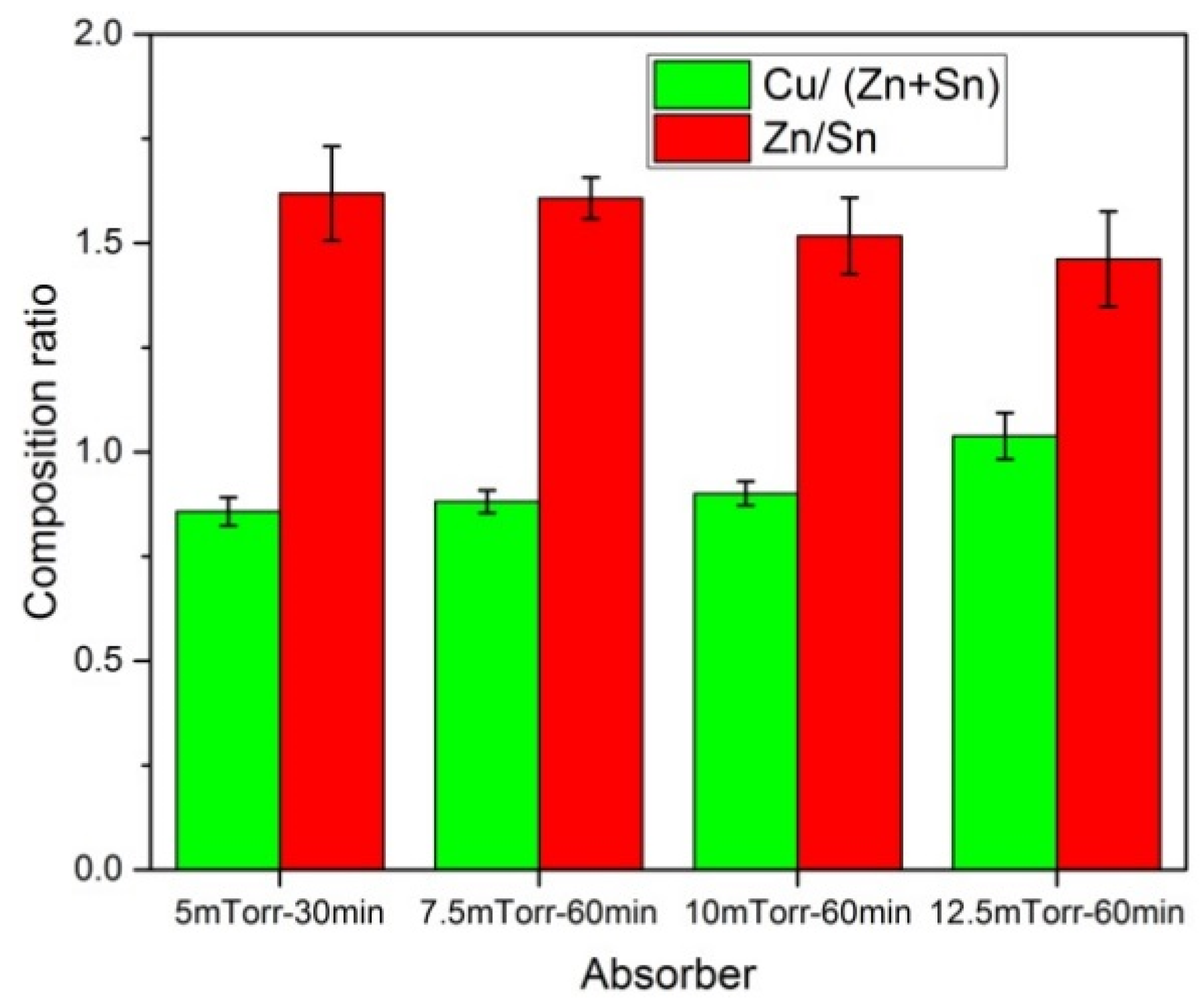
Figure 1 shows the chemical composition of CZTS absorbers with precursors deposited at different pressures and durations. It indicates that the Zn/Cu ratio decreases and the Cu/(Zn + Sn) ratio increases with increasing deposition pressure. This suggests that the Cu sputtering rate increased, yet the Zn sputtering rate decreased with increasing pressure, assuming a constant Sn deposition rate. The composition of the sulfurised CZTS films is Cu/(Zn + Sn) 0.9, and Zn/Sn 1.55. The Cu/(Zn + Sn) is large whereas Zn/Sn is not in the desired range (Cu/(Zn + Sn) = 0.8–0.9, Zn/Sn = 1.2–1.3) reported for high efficiency CZTS solar cells [11]. The assumption for putting 5 mT-30 min the comparison group is that the film quality would not change over a deposition duration of 60 min, which should be largely valid.
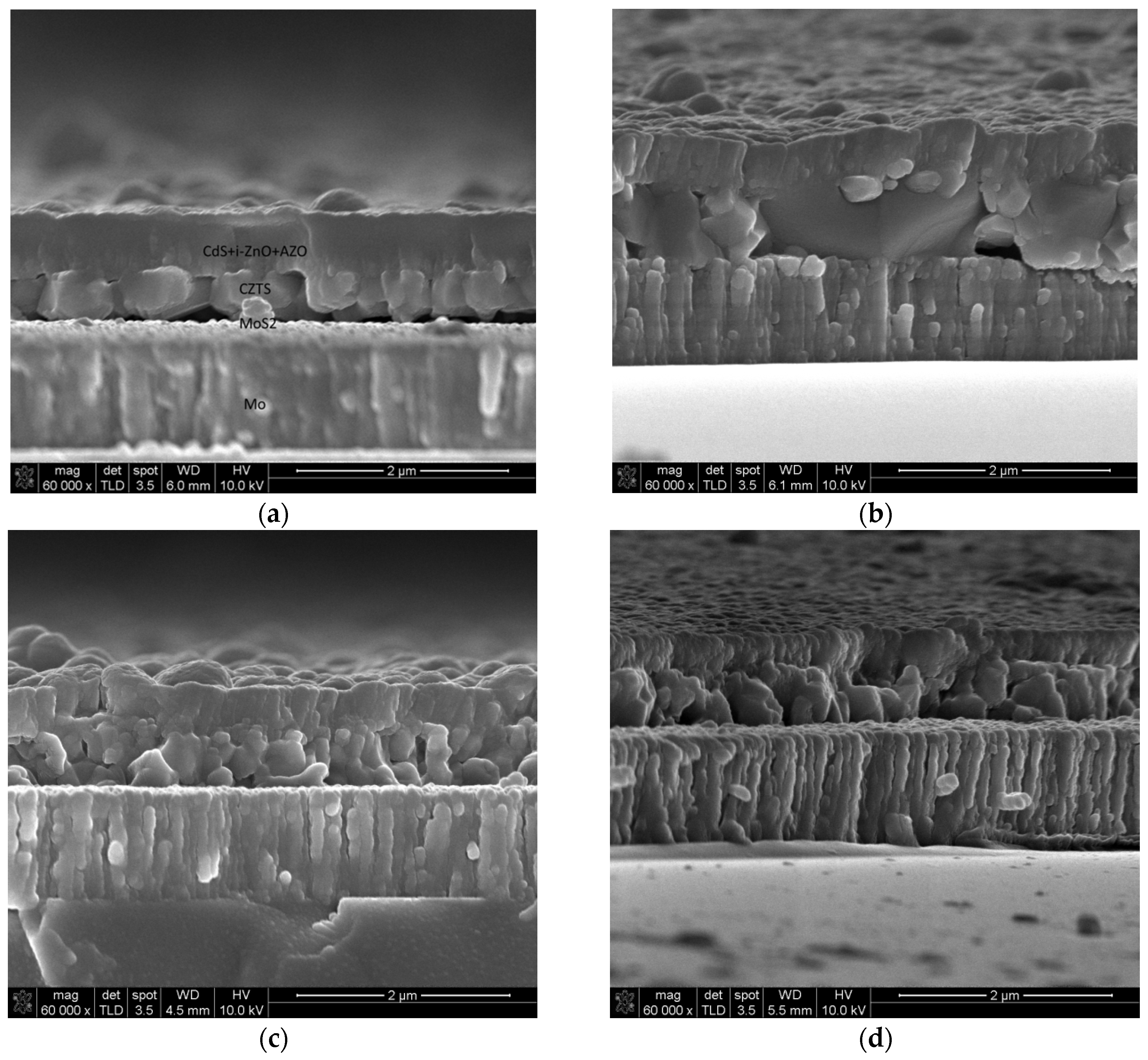
Figure 2 shows SEM cross sectional images of the CZTS absorbers fabricated from different precursors. Figure 2a indicates that the 5 mTorr-30 min absorber is mainly composed of large grains spanning the whole thickness growing from the surface to the back contact, yet it has a large amount of voids at the back contact region as well as the junction region, and a film thickness of only 370 nm, almost half of the 7.5 mTorr-60 min absorber. The thickness is as expected for a 30 min deposition duration in comparison with 60 min for 7.5 mTorr-60 min. The voids at the back contact region may be due to the reaction of CZTS with Mo and a small absorber thickness, which led to a very limited amount of time for the formation and growth of the CZTS absorber and a long time for the decomposition reaction [12,13]. The voids at the junction region may reduce the short wavelength absorption and therefore carrier generation for near blue light. Figure 2b–d shows a mixture of large grains and small grains with a few voids for the 7.5 mTorr-60 min absorber, largely small grains for the 10 mTorr-60 min absorber, and mainly small grains with voids at the back contact region for the 12.5 mTorr-60 min absorber, respectively. The voids in the 12.5 mTorr-60 min absorber may be caused by the Cu rich composition, because the excess Cu may either diffuse into the Mo contact [14] or get re-absorbed into the CZTS absorber owing to a high composition tolerance for single phase CZTS at high sulfurization temperature, and leave voids behind [7,12]. The small grain size may result in high recombination at the grain boundary if not properly passivated and could therefore degrade the open circuit voltage (VOC). Voids may not only do similar damage to VOC due to dangling bonds on the surface but could also short circuit the current density (JSC) owing to the voids that block current collection or shunt path formation. In contrast, the large grains from 5 mTorr-30 min and 7.5 mTorr-60 min may have low recombination and high efficiency. Also very interestingly, the absorber film surface is generally smooth (10 mTorr-60 min gives the roughest surface) and the thickness decreased with deposition pressure: 740 nm for 7.5 mTorr-60 min, 590 nm for 7.5 mTorr-60 min, and 555 nm for 12.5 mTorr-60 min, respectively. This would result in different light reflection, absorption, and carrier generation depth profiles. A slightly rough surface may produce an anti-reflection effect due to the double bounce of light. On the other hand, a smooth surface may reduce the series resistance, the formation of possible shunt circuits, and enhance carrier collection.
To check on the structural properties of the films in more detail, the films were characterized by XRD and Raman spectroscopy.
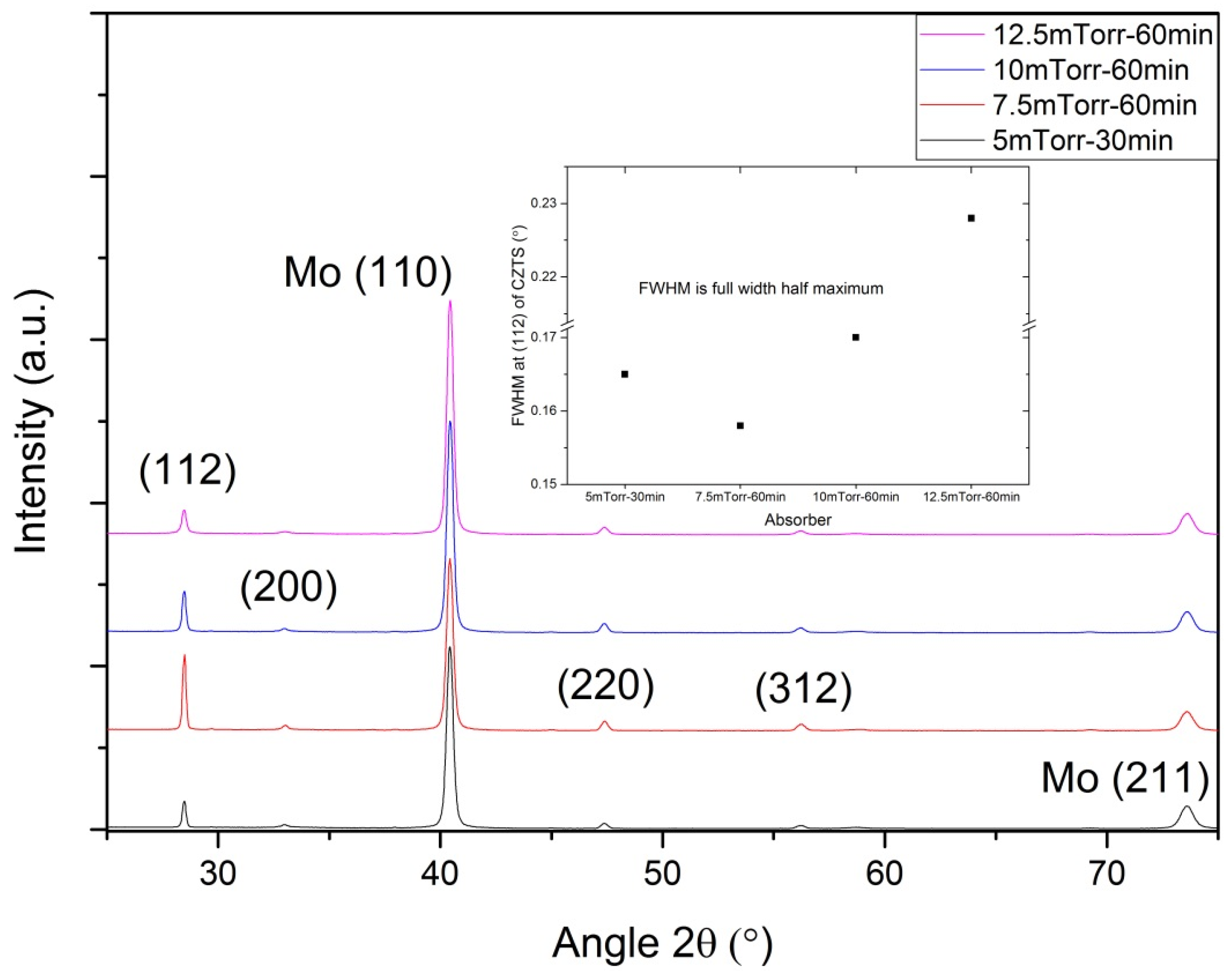
Figure 3 presents the XRD patterns of the CZTS absorbers with varying precursor deposition parameters. It demonstrates that all absorbers share a very similar pattern which agrees well with that of tetragonal kesterite CZTS (JCPDS No. 026-0575) with the preferred orientation of CZTS at (112) consistent with the literature [15,16]; the full width at half maximum (FWHM) of the main peak (112) of CZTS has a small dip down from 0.165° to 0.158°, then increases by 0.17° and ends at 0.228° with increasing the precursor deposition pressure from 5 to 12.5 mTorr. This FWHM trend is consistent with the SEM results as small FWHM reflects large grain size and a low defect level inside the film. It implies improved crystallinity in the following order: 12.5 mTorr-60 min, 10 mTorr-60 min, 5 mTorr-30 min, 7.5 mTorr-60 min. There are a large amount of voids in the 5 mTorr-30 m absorber and therefore its crystallinity degrades, and is not as good as 7.5 mTorr-60 min.
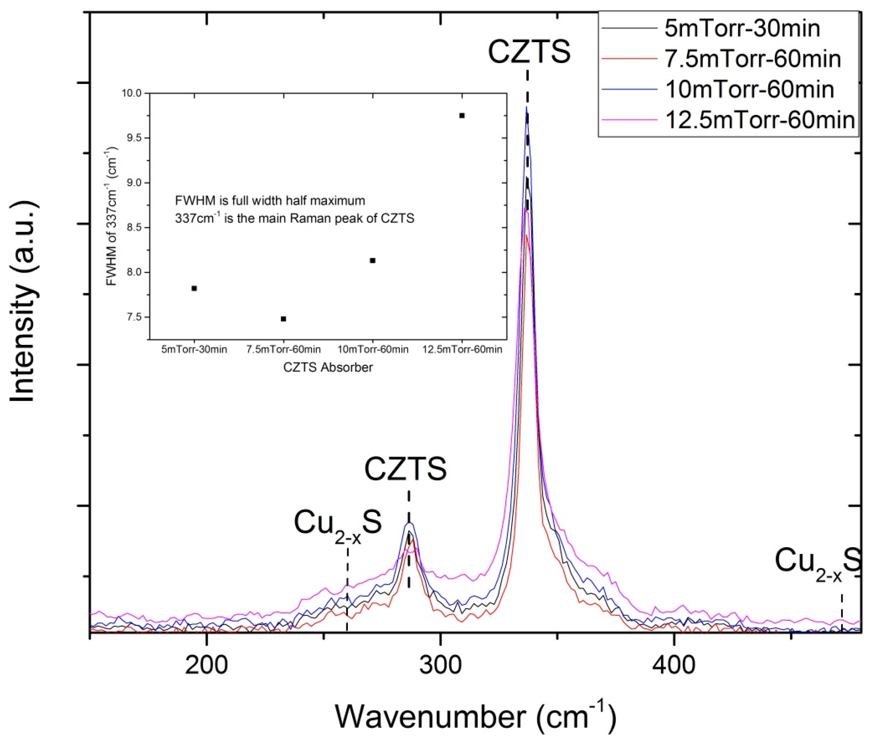
Figure 4 shows the Raman spectra of the absorbers. It reveals that all absorbers share very similar Raman spectra indicating peaks of the dominant CZTS phase with no other apparent phases. It shows an asymmetric Raman main peak at 337 cm−1 which matches well with other researchers’ findings in the literature [17,18]. The peak asymmetry was believed to be accounted for by phone confinement and strain, especially for small grain sized polycrystalline CZTS film [18]. The Cu2−xS peak marked by dashed lines is equivalent to being not observable for all the absorbers, with only a tiny hillock for 12.5 mTorr-60 min. The FWHM of CZTS’s main peak at 337 cm−1 also has a small dip down from 7.82 to 7.48 cm−1, and then increases by 8.13 cm−1 and ends at 9.75 cm−1 with the increasing precursor deposition pressure. This trend matches with the FWHM of the (112) peak in Figure 3. Raman FWHM of the main peak also reflects the crystal structural quality of the absorber and therefore discloses the same crystallinity trend of the absorbers as with XRD FWHM.
The influence of the chemical and structural properties on the optical and electrical properties of completed devices is discussed in the following section.
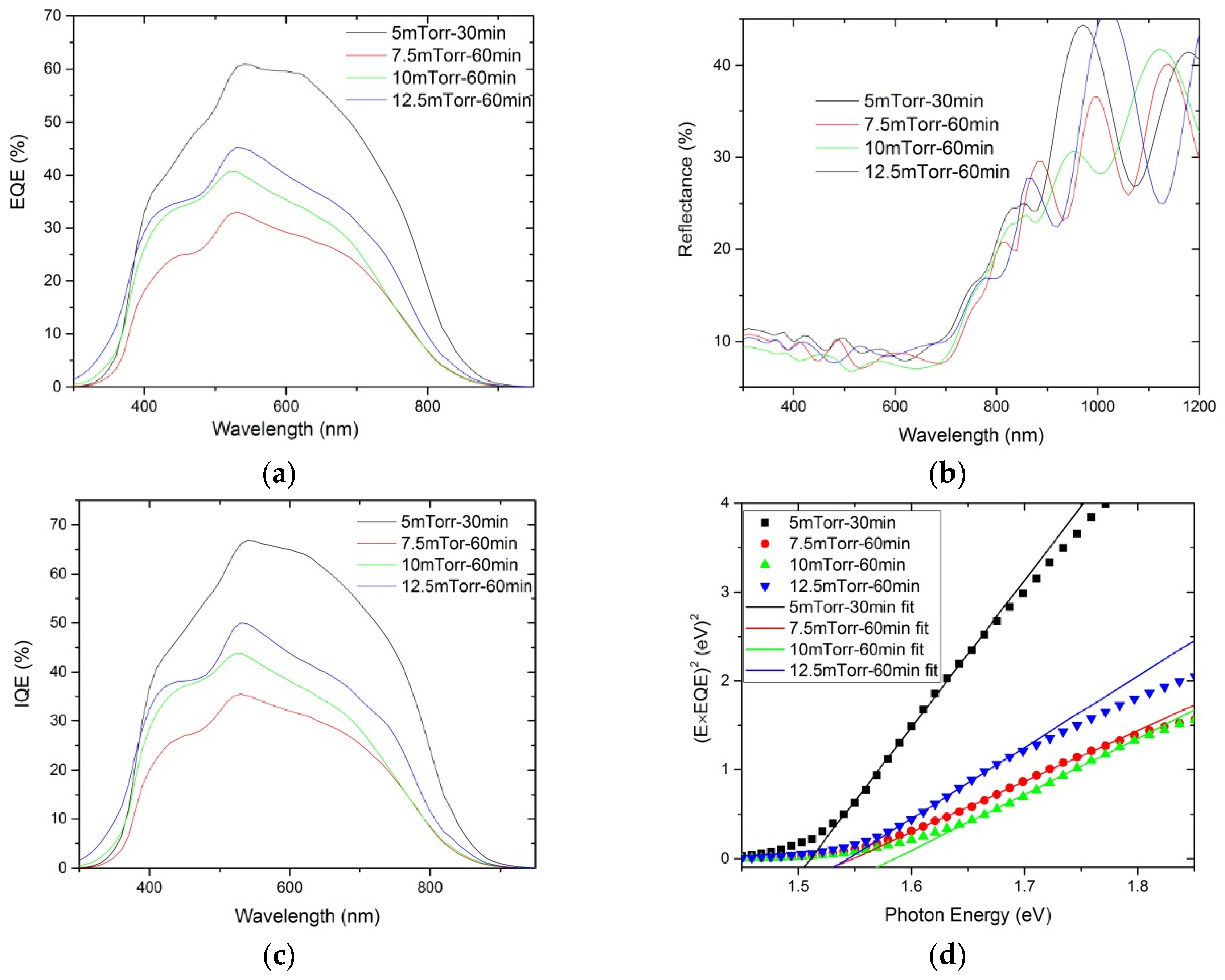
Figure 5 shows external quantum efficiency (EQE), reflection (R), internal quantum efficiency (IQE = EQE/(1 − R)), and (EQE × E)2 versus photon energy E of all completed devices with varying precursors. Figure 5a shows that low pressure deposited samples give high QE almost in the whole wavelength range of interest, except that 5 mTorr-30 min has a rather low QE for the near blue light (300–400 nm) range due to voids in the junction region. Figure 5b demonstrates that 5 mTorr-30 min has the highest reflection owing to its lowest thickness, and 10 mTorr-60 min features the lowest reflection thanks to its second highest thickness as well as the roughest surface in the group in the wavelength range from 300 to 800 nm. For wavelength ranges above this range, a thick film results in low reflection and therefore high absorption. Figure 5c reflects direct carrier collection efficiency over the whole spectrum of the solar cells excluding optical effects, yet IQE reflects the same with EQE. It means that voids in the junction region of 5 mTorr-30 min also affect the properties of the localized part of the junction and therefore the collection efficiency of the carriers. The minority carrier collection efficiency or the carrier collection depth is generally the depletion region width plus the minority carrier diffusion length assuming zero recombination in the above region. In reality, the heterojunction interface is not perfect and a cliff-like band alignment [19] between the conduction bands of CZTS and CdS generally leads to high recombination which would be deteriorated by lattice mismatch between CZTS and CdS; meanwhile, a back contact region is generally a high recombination region because the detrimental reaction between CZTS and Mo lead to secondary phases and voids. In the literature, a 350 nm diffusion length gives an efficiency up to 8.4% [20]; and the depletion region width is generally only within 100 nm for a 6.2% solar device [21]. This suggests that only within 450 nm thickness of absorber is contributing to carrier generation and collection. Additionally, Electron Beam Induced Current (EBIC) images indicate that even the reduced-void CZTS solar cell shows almost negligible carrier collection at the back contact region [22]. The major carrier generation as well as collection was mainly in the top junction region plus a diffusion length, and the back contact region acted as a recombination sink, not only trapping but also promoting recombination. Therefore, the thick absorber resulted in less effective light absorption, yet high recombination, over the large in-effective regions. This chiefly explains why 5 mTorr-30 min was the best QE performer. On top of the appropriate absorber thickness close to the carrier collection depth, large grain size is also an indispensable factor for device performance.
Figure 5d is based on a linear fitting of (EQE × E)2 vs. E to obtain the intercept on the E axis, which is the bandgap of the absorber [23]. It shows that the bandgaps of 5 mTorr-30 min, 7.5 mTorr-60 min, 10 mTorr-60 min, and 12.5 mTorr-60 min are 1.505, 1.535, 1.57, and 1.535 eV, respectively. A large band gap ordinarily has high open circuit voltage.
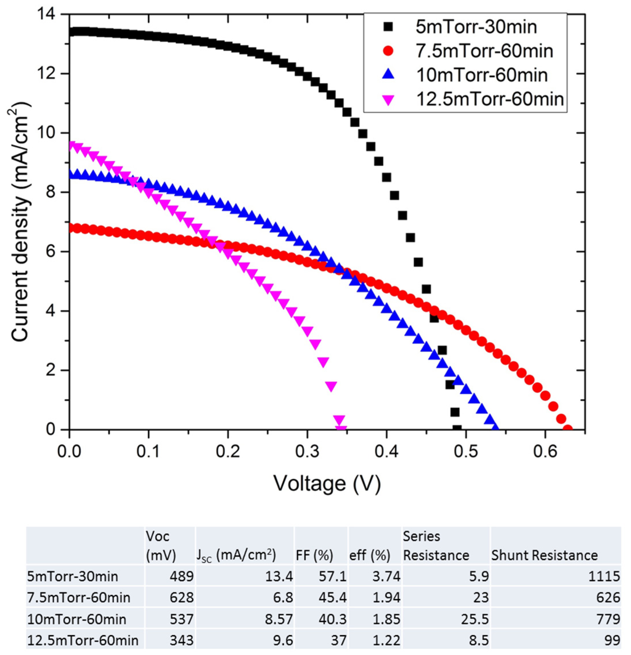
Figure 6 is the light I-V results of the solar cells. The 5 mTorr-30 min absorber has the highest JSC of 13.4 mA/cm2, fill factor of 57.1%, and shunt resistance of 1115 Ω·cm2, yet has the lowest series resistance of 5.9 Ω·cm2 and therefore the highest efficiency of 3.74% thanks to the essentially similar absorber thickness with the effective carrier collection depth plus large grain size, which to the authors’ knowledge is also the record efficiency for stoichiometric single target sputtering CZTS devices; however, it has the second lowest VOC mainly due to the voids and low bandgap as discussed above. 7.5 mTorr-60 min has the largest VOC thanks to the high crystallinity of the material, while it has the lowest JSC caused predominantly by a much thicker high recombinative bottom region together with voids relevant blocking effect or shunting effect. The thick recombinative bottom region not only increased the series resistance dramatically but also reduced the effective light absorption and photogeneration. The lowest VOC of 12.5 mTorr-60 min can be roughly ascribed to the lowest crystallinity of the absorber material and the highest Cu content (a relatively high copper concentration ratio was reported to cause short lifetimes and therefore low VOC [24]) with voids relevant recombination a minor factor.

4. Conclusions

A record efficiency of 3.74% was achieved for single stoichiometric target sputtering CZTS solar cells at a low processing pressure of 5 mTorr and a short duration of 30 min. Such parameters yield the highest EQE, JSC, FF, shunt resistance, and efficiency by virtue of mostly the appropriate absorber thickness which is close to the minority carrier collection depth. The relatively low VOC may be due to a large amount of voids within the absorber and the low bandgap. Interestingly, high pressure resulted in thin absorber thickness, leading to high EQE and JSC, yet much lower VOC and FF, which may be chiefly caused by low crystallinity and high Cu concentration. Low pressure leads to large grain size and narrow FWHM of major XRD and Raman peaks. These suggest that thin absorbers of 450 nm thickness and low pressure deposition of the precursor would be necessary for future high efficiency single target CZTS solar cells.

Acknowledgments

This Program has been supported by the Australian Government through the Australian Renewable Energy Agency and the Australian Research Council, and by the China Guodian Corporation. Responsibility for the views, information, or advice expressed herein is not accepted by the Australian Government. The authors acknowledge the facilities of the Electron Microscope Unit of The University of New South Wales. CUI acknowledges the Discovery Early Career Researcher Award, grant # DE160101252.

Author Contributions

Hongtao Cui and Xiaolei Liu conceived and designed the experiments; Xiaolei Liu, Fangyang Liu and Chang Yan performed the experiments; Hongtao Cui and Lingling Sun analyzed the data; Xiaojing Hao contributed reagents/materials/analysis tools; Hongtao Cui wrote the paper.

Conflicts of Interest

The authors declare no conflict of interest. The founding sponsors had no role in the design of the study; in the collection, analyses, or interpretation of data; in the writing of the manuscript, and in the decision to publish the results.

References

  1. Peter, L.M. Towards sustainable photovoltaics: The search for new materials. Phil. Trans. R. Soc. A 2011, 369, 1840–1856. [Google Scholar] [CrossRef] [PubMed] [Green Version]
  2. Mitzi, D.B.; Gunawan, O.; Todorov, T.K.; Barkhouse, D.A.R. Prospects and performance limitations for Cu–Zn–Sn–S–Se photovoltaic technology. Phil. Trans. R. Soc. A 2013, 371. [Google Scholar] [CrossRef] [PubMed]
  3. Song, X.; Ji, X.; Li, M.; Lin, W.; Luo, X.; Zhang, H. A review on development prospect of CZTS based thin film solar cells. Int. J. Photoenergy 2014. [Google Scholar] [CrossRef]
  4. Xie, M.; Zhuang, D.; Zhao, M.; Zhuang, Z.; Ouyang, L.; Li, X.; Song, J. Preparation and characterization of Cu2ZnSnS4 thin films and solar cells fabricated from quaternary Cu-Zn-Sn-S target. Int. J. Photoenergy 2013, 2013. [Google Scholar] [CrossRef]
  5. Nakamura, R.; Tanaka, K.; Uchiki, H.; Jimbo, K.; Washio, T.; Katagiri, H. Cu2ZnSnS4 thin film deposited by sputtering with Cu2ZnSnS4 compound target. J. Jpn. Appl. Phys. 2014, 53. [Google Scholar] [CrossRef]
  6. Katagiri, H.; Jimbo, K. Development of rare metal-free CZTS-based thin film solar cells. In Proceedings of the 37th IEEE Photovoltaic Specialists Conference, Seattle, WA, USA, 19–24 June 2011; pp. 003516–003521.
  7. Chagarov, E.; Sardashti, K.; Haight, R.; Mitzi, D.B.; Kummel, A.C. Density-functional theory computer simulations of CZTS0.25Se0.75 alloy phase diagrams. J. Chem. Phys. 2016, 145. [Google Scholar] [CrossRef]
  8. Zhang, K.; Su, Z.; Zhao, L.; Yan, C.; Liu, F.; Cui, H.; Hao, X.; Liu, Y. Improving the conversion efficiency of Cu2ZnSnS4 solar cell by low pressure sulfurization. Appl. Phys. Lett. 2014, 104, 141101. [Google Scholar] [CrossRef]
  9. Cui, H.; Liu, X.; Liu, F.; Hao, X.; Song, N.; Yan, C. Boosting Cu2ZnSnS4 solar cells efficiency by a thin Ag intermediate layer between absorber and back contact. Appl. Phys. Lett. 2014, 104, 041115. [Google Scholar] [CrossRef]
  10. Cui, H.; Li, W.; Liu, X.; Song, N.; Lee, C.; Liu, F.; Hao, X. Optimization of precursor deposition for evaporated Cu2ZnSnS4 solar cells. Appl. Phys. A 2015, 118, 893–899. [Google Scholar] [CrossRef]
  11. Mitzi, D.B.; Gunawan, O.; Todorov, T.K.; Wang, K.; Guha, S. The path towards a high-performance solution-processed kesterite solar cell. Solar Energy Mater. Solar Cells 2011, 95, 1421–1436. [Google Scholar] [CrossRef]
  12. Scragg, J.J.; Watjen, J.T.; Edoff, M.; Ericson, T.; Kubart, T.; Platzer-Bjorkman, C. A detrimental reaction at the molybdenum back contact in Cu2ZnSn(S,Se)4 thin-film solar cells. J. Am. Chem. Soc. 2012, 134, 19330–19333. [Google Scholar] [CrossRef] [PubMed]
  13. Scragg, J.J. Copper Zinc Tin Sulfide Thin Films For Photovoltaics: Synthesis and Characterisation by Electrochemical Methods; Springer: Berlin, Germany, 2011. [Google Scholar]
  14. Liu, F.; Sun, K.; Li, W.; Yan, C.; Cui, H.; Jiang, L.; Hao, X.; Green, M.A. Enhancing the Cu2ZnSnS4 solar cell efficiency by back contact modification: Inserting a thin TiB2 intermediate layer at Cu2ZnSnS4/Mo interface. Appl. Phys. Lett. 2014, 104, 051105. [Google Scholar] [CrossRef]
  15. Thota, N.; Gurubhaskar, M.; Sunil, M.A.; Prathap, P.; Subbaiah, Y.P.V.; Tiwari, A. Effect of metal layer stacking order on the growth of Cu2ZnSnS4 thin films. Appl. Surf. Sci. 2017, 396, 644–651. [Google Scholar] [CrossRef]
  16. Sarswat, P.K.; Snure, M.; Free, M.L.; Tiwari, A. CZTS thin films on transparent conducting electrodes by electrochemical technique. Thin Solid Films 2012, 520, 1694–1697. [Google Scholar] [CrossRef]
  17. Sarswat, P.K.; Free, M.L.; Tiwari, A. Temperature-dependent study of the raman a mode of Cu2ZnSnS4 thin films. Phys. Status Solidi B 2011, 248, 2170–2174. [Google Scholar] [CrossRef]
  18. Sarswat, P.K.; Free, M.L. The effects of dopant impurities on Cu2ZnSnS4 system Raman properties. J. Mater. Sci. 2015, 50, 1613–1623. [Google Scholar] [CrossRef]
  19. Yan, C.; Liu, F.; Song, N.; Ng, B.K.; Stride, J.A.; Tadich, A.; Hao, X. Band alignments of different buffer layers (CdS, Zn(O,S), and In2S3) on Cu2ZnSnS4. Appl. Phys. Lett. 2014, 104, 173901. [Google Scholar] [CrossRef]
  20. Shin, B.; Gunawan, O.; Zhu, Y.; Bojarczuk, N.A.; Chey, S.J.; Guha, S. Thin film solar cell with 8.4% power conversion efficiency using an earth-abundant Cu2ZnSnS4 absorber. Prog. Photovolt. Res. Appl. 2013, 21, 72–76. [Google Scholar] [CrossRef]
  21. Dhakal, T.P.; Peng, C.-Y.; Tobias, R.R.; Dasharathy, R.; Westgate, C.R. Characterization of a CZTS thin film solar cell grown by sputtering method. Solar Energy 2014, 100, 23–30. [Google Scholar] [CrossRef]
  22. Sugimoto, H.; Hiroi, H.; Sakai, N.; Muraoka, S.; Katou, T. Over 8% efficiency Cu2ZnSnS4 submodules with ultra-thin absorber. In Proceedings of the 38th IEEE Photovoltaic Specialists Conference, Austin, TX, USA, 3–8 June 2012; pp. 002997–003000.
  23. Ahmed, S.; Reuter, K.B.; Gunawan, O.; Guo, L.; Romankiw, L.T.; Deligianni, H. A high efficiency electrodeposited Cu2ZnSnS4 solar cell. Adv. Energy Mater. 2012, 2, 253. [Google Scholar] [CrossRef]
  24. Sugimoto, H.; Liao, C.; Hiroi, H.; Sakai, N.; Kato, T. Lifetime Improvement for High Efficiency Cu2ZnSnS4 Submodules. In Proceedings of the 39th IEEE Photovoltaic Specialists Conference, Tampa, FL, USA, 16–21 June 2013; pp. 3208–3211.
Figure 1. Chemical composition (atomic ratios of Cu/(Zn + Sn) and Zn/Sn) of sulfurized Cu2ZnSnS4 (CZTS) absorbers with precursors deposited at different pressures and durations: 5 mTorr-30 min is the deposition condition: 50 mTorr pressure and 30 min duration.
Coatings 07 00019 g001
Figure 2. SEM cross section images of CZTS absorbers prepared from different precursors: (a) 5 mTorr-30 min, (b) 7.5 mTorr-60 min, (c) 10 mTorr-60 min, and (d) 12.5 mTorr-60 min.
Coatings 07 00019 g002
Figure 3. XRD patterns of CZTS absorbers fabricated from various precursors: 5 mTorr-30 min, 7.5 mTorr-60 min, 10 mTorr-60 min, and 12.5 mTorr-60 min.
Coatings 07 00019 g003
Figure 4. Raman spectra of CZTS absorbers fabricated from varying precursors: 5 mTorr-30 m, 7.5 mTorr-60 min, 10 mTorr-60 min, and 12.5 mTorr-60 min. The inlet picture shows the full width half maximum (FWHM) of the Raman peak at 337 cm−1 which is obtained by fitting the peaks with mixed Gaussian–Lorentzian using GRAMS/AI spectroscopic software (version 9.0R2, Thirmo Fisher Scientific Inc, Waltham, MA, USA).
Coatings 07 00019 g004
Figure 5. (a) External quantum efficiency (EQE) of CZTS devices with different precursor deposition parameters: 5 mTorr-30 min, 7.5 mTorr-60 min, 10 mTorr-60 min, and 12.5 mTorr-60 min; (b) Reflectance of samples in Figure 5a; (c) Internal quantum efficiency (IQE) of samples in Figure 5a; (d) Band gap estimation plot (E × EQE)2 versus E, where E is the photon energy.
Coatings 07 00019 g005
Figure 6. Light JV curve of CZTS devices fabricated from different precursors: 5 mTorr-30 min, 7.5 mTorr-60 min, 10 mTorr-60 min and 12.5 mTorr-60 min. The efficiency, VOC, JSC, fill factor (FF), shunt resitance (in Ω·cm2), and series resistance (in Ω·cm2) are given in the inset table.
Coatings 07 00019 g006

