
Contamination-Free Graphene Transfer from Cu-Foil and Cu-Thin-Film/Sapphire

1
Department of Materials Science and Engineering, Ajou University, Suwon 16499, Korea
2
Department of Energy Systems Research, Ajou University, Suwon 16499, Korea
*
Author to whom correspondence should be addressed.
Coatings 2017, 7(12), 218; https://doi.org/10.3390/coatings7120218
Submission received: 7 November 2017
/
Revised: 24 November 2017
/
Accepted: 27 November 2017
/
Published: 2 December 2017
(This article belongs to the Special Issue Graphene and Other 2D Layered Nanomaterial-Based Films: Synthesis, Properties and Applications)
Abstract
:The separation of graphene grown on metallic catalyst by chemical vapor deposition (CVD) is essential for device applications. The transfer techniques of graphene from metallic catalyst to target substrate usually use the chemical etching method to dissolve the metallic catalyst. However, this causes not only high material cost but also environmental contamination in large-scale fabrication. We report a bubble transfer method to transfer graphene films to arbitrary substrate, which is nondestructive to both the graphene and the metallic catalyst. In addition, we report a type of metallic catalyst, which is 700 nm of Cu on sapphire substrate, which is hard enough to endure against any procedure in graphene growth and transfer. With the Cr adhesion layer between sapphire and Cu film, electrochemically delaminated graphene shows great quality during several growth cycles. The electrochemical bubble transfer method can offer high cost efficiency, little contamination and environmental advantages.
1. Introduction
Graphene, a two-dimensional honeycomb structure of carbon isotopes, is receiving worldwide attention due to its superior quality, such as high carrier mobility, excellent strength and high thermal conductivity [1,2]. Due to its high electrical conductivity, transparency, and flexibility, high-quality single-layer graphene with large area has received much attention in the industry [3,4,5]. However, the conventional method of transferring graphene essentially involves a chemical etching step to remove the metal substrate, which causes environmental pollution and damage to graphene, as well as an increase in the production cost [6]. In addition, it is not appropriate to transfer the graphene from some chemically inactive metal catalysts such as Ru, Au, and Pt because these types of metals are hard to remove completely and etching is costly. Recently, bubble-transfer method, which use electrochemical reaction to delaminate graphene from catalyst metal, was reported [7,8,9,10]. In this way, it is possible to save metal catalyst to synthesize graphene by re-using the catalyst. However, this method (conventionally using Cu foil of about 25 μm thickness) can cause other damages to the Cu foil during handling such as wrinkling, tearing, and vacuum retention in spin coating, resulting in defects in synthesized graphene.
Here we report the growth of graphene on three types of Cu catalysts. First, a conventional Cu foil was used [11,12]. Second, a Cu film deposited on a sapphire substrate without any other layer or processing was used [13,14]. Finally, we used a Cu film on a sapphire substrate with a Cr adhesive layer [15]. In these three samples, graphene was grown by CVD and transferred from Cu to target substrate by bubble transfer method. The sapphire substrate is robust enough to withstand mechanical damage, preventing Cu from tearing and wrinkling. In addition, the Cr layer between the sapphire and the Cu thin film improves the adhesion strength between both surfaces to prevent Cu film from peeling and tearing. Further, since Cr is more reactive than Cu, it also has an effect of preventing Cu from being oxidized. Therefore, this non-destructive method makes it possible to use the Cu film catalyst repeatedly without damages, and the synthesized graphene has almost the same quality as the original one.
2. Materials and Methods
2.1. Preparation
2.1.1. Catalyst Materials Preparation
(i) Commercial Cu foil (Alfa Aesar, Ward Hill, MA, USA, item no. 13382, 99.8% purity) which were first immersed for 1 min in 0.1 mole ammonium persulfate ((NH4)2S2O8, Sigma-Aldrich, St. Louis, MO, USA, item no. 248614, ACS reagent, 98.0%) solution to clean and etch the contaminants on the surface of the Cu foil; (ii) 700 nm Cu film on c-plane sapphire and (iii) 700 nm Cu film on adhesion layer (15 nm Cr) coated c-plane sapphire were prepared by using electron-beam evaporator (substrate temperature was room temp and chamber pressure was maintained at 0.05 mTorr during deposition).
2.1.2. CVD Process
Each catalyst is loaded into a quartz tube reaction chamber to perform graphene growth. The pressure in the chamber was pumped to 5 mTorr using a mechanical pump, then hydrogen (H2) was injected into the chamber at 40 sccm. Then, the Cu film catalysts (Cu/c-sapphire and Cu/Cr/c-sapphire) temperature increased to 950 °C over 60 min. The reduction step of copper was done by flowing hydrogen gas at this stage. The pressure in the chamber is maintained at 500 mTorr. Then, methane (CH4) gas was introduced into the chamber at 10 sccm for 10 min. Finally, furnace was rapidly cooled to room temperature to precipitate the graphene on the catalyst surface under a hydrogen gas flow of 40 sccm. For the Cu foil catalyst, the catalyst was heated to 1000 °C for 60 min and annealed during 30 min to increase grain size of Cu before methane injection, and the other step was the same with Cu film catalysts.
2.2. Bubble Transfer
After growth, the graphene sample was spin-coated with poly-methyl methacrylate (PMMA) at 1800 rpm for 40 s and dried in air for 10 min. 1 M NaOH aqueous solution was used in the electrolyte for constant current and voltage, 40 mA and 3 V. A platinum film was used as the electrode. The delaminated graphene/PMMA film was transferred to Si/SiO2 substrate. The transferred graphene was heated at 180 °C for 30 min and then cleaned in acetone for 1 h. After that, it was cleaned in Isopropyl Alcohol (IPA) and Deionized (DI) water for 10 min each.
2.3. Analysis
Scanning electron microscope (SEM) images were taken using a JSM-6700 (JEOL, Tokyo, Japan) device at 5.0 kV. The Optical Microscope (OM) images were taken with a U-MSSP49 (Olympus, Tokyo, Japan) microscope. Raman spectra were obtained with a LabRAM HR Evolution—Nicolet iS50 (Jobin Yvon, Horiba, Kyoto, Japan) spectrometer under He–Ne 532 nm laser wavelength, 5 mm in diameter.
3. Results and Discussion
3.1. Bubble Transfer Method for Transferring Graphene
Figure 1 illustrates the limitations of the conventional graphene transfer method. The OM image in Figure 1a shows some voids and graphene flakes attached to the graphene. These voids are defects that occur during the transfer process. When there is an unattached region between the target substrate and the graphene, the graphene is teared and scratched during the process to dissolving PMMA [16,17,18]. For the graphene flakes, since the graphene synthesized on the copper foil grows on both sides of the foil, if it is not removed by the oxygen plasma, the residue as shown in Figure 1a remains beneath the surface. The oxygen plasma process is, however, a demanding process and can cause mechanical damage to the Cu foil during the handling process. The bubble transfer process allows clean graphene to be obtained without the oxygen plasma process. The bubble transfer method does not cause such damages to graphene, and only one side of the graphene can be clearly peeled off. Furthermore, it can also reduce the loss of Cu compared to the conventional chemical etching transfer method. Since the binding energy between graphene and Cu (0.033 eV per carbon atom) is relatively weak compared to the inter-planar bond strength of graphite, the graphene can be easily peeled off from Cu by the bubble transfer method [19,20,21]. Figure 1c shows a schematic view of bubble transfer. A copper foil/graphene/PMMA was used as the cathode, a platinum foil was used as the anode, and NaOH solution was used as the electrolyte. When direct current is applied, water is reduced on the surface of the Cu foil to generate hydrogen. When this hydrogen bubble occurs in large quantities between copper and graphene, the graphene/PMMA layer is separated from copper within seconds. PMMA coatings of sufficient thickness and concentration are needed, since thin PMMA/graphene film can be damaged by hydrogen bubbles or water [22,23]. The mass change of copper foil was measured during repeated CVD deposition and shown in Table 1. Compared to the original Cu foil which was 0.0235 g at first, it decreased by 0.0064 g for seven cycles. There was a decrease of about 0.001 g in one cycle. A slight reduction of about 4% per cycle is believed to have occurred during the repeated pre-etching and CVD processes as well as during the bubble transfer process.
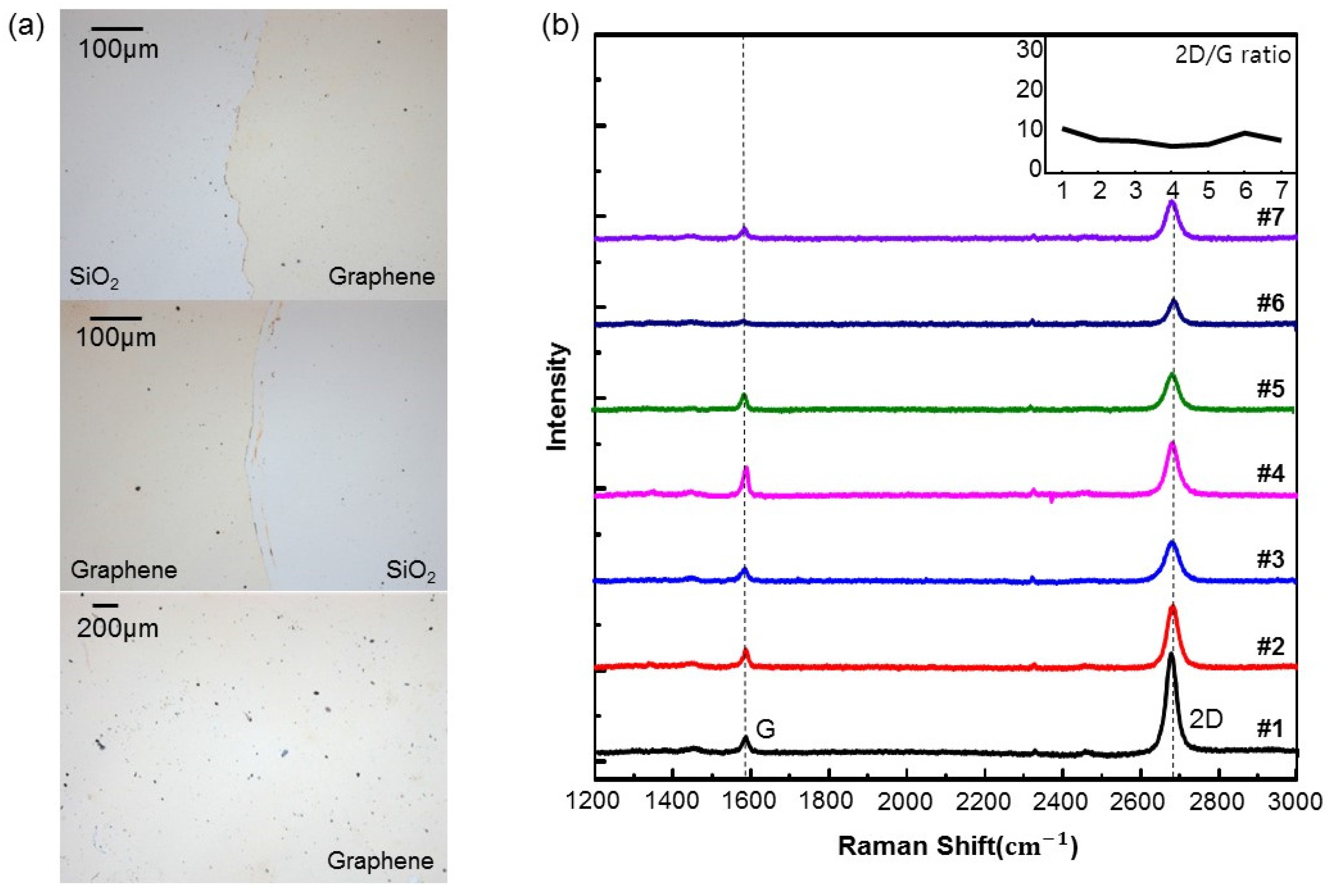
In Figure 2, we analyzed the performance of graphene films made for seven cycles using a single Cu foil. As shown in Figure 2a, graphene films separated by the “bubble transfer” method have a considerably smaller amount of backside graphene residue which can trap the metal catalyst between transferred graphene film and backside graphene flake. Although not all metal residues can be eliminated with this method because the metal residues can exist not only at trapped surface but also at any other morphological feature such as grain boundaries, wrinkles, graphene adlayer, etc., it can be relatively reduced [24]. Additional research is needed to eliminate them. Figure 2b shows the Raman spectrum of seven graphene films with very high 2D/G peak ratio of about 3 to 10. This means that the synthesized graphene is close to a single layer. In addition, the very low intensity of the D-peak located at about 1350 cm−1 indicates that the qualities of these graphene films is very good. However, when Cu foil is used, the Cu foil may be damaged, torn or scratched by other transfer processes than bubble transfer (it even wrinkled easily with tweezers). Vacuum stamping, which is inevitable especially when spin coating PMMA, must be removed because it greatly degrades the performance of the graphene. So, we have grown a copper film on a sapphire substrate that is easy to handle in process and used it for graphene growth. C-plane sapphire (0001) was used due to low lattice mismatch with Cu (111) which is the most suitable catalytic surface for the hexagonal shaped graphene growth.
3.2. Effect of Cr Adhesive Layer
As shown in Figure 3, the adhesion between Cu and sapphire is poor, and Cu tends to peel off even once in bubble transfer. This is because bubble transfer is an electrochemical process that causes desorption on both sides of Cu. Figure 3b is an Optical Microscope (OM) image of a Cu surface after short-time electrolysis. As can be seen in the figure, the Cu layer is swollen, and when they are combined to some extent, they are separated from the sapphire substrate as shown in Figure 3a. To solve this problem, we added a Cr layer between Cu and sapphire. The Cr layer acts as an adhesive layer and strengthens the attraction between Cu and sapphire. Figure 3c shows the surface of a sample having a Cr layer after electrolysis, which is the same process as shown in Figure 3b. It is relatively more clean and well maintained than the former. We used XRD analysis to understand this effect (Figure 4). The status of Cu was compared by analyzing the XRD of Cu/Sapphire and Cu/Cr/Sapphire samples before and after 950 °C CVD graphene growth. The Cu (100)/Cu (200) intensity ratios of the two samples were 28 and 2.6 before the CVD process, respectively. Since the sapphire (0001) plane and the Cu (111) plane are hexagonal planes, the previous sample deposited directly on the sapphire is deposited in the (111) preferred orientation, unlike the latter where the Cr layer with the BCC structure is present [25,26]. It changes greatly after the CVD process. At high temperatures, the intensity of the (111) peak increases and the intensity of the (200) peak decreases due to Cu agglomeration.
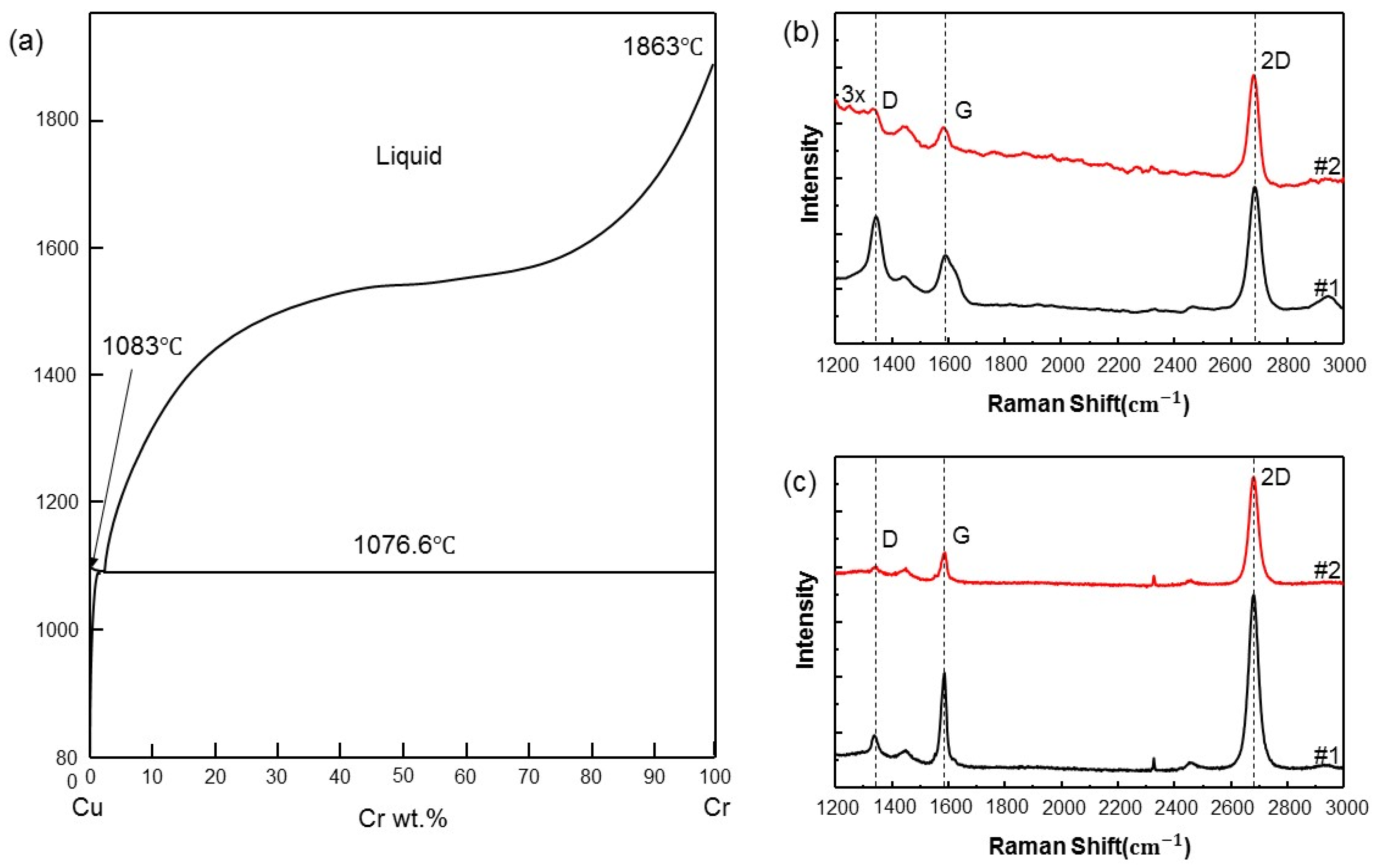
This means that Cu does not adhere well to the sapphire surface, and the performance of the Cu catalyst also deteriorates. The surface roughness of Cu is also expected to increase by agglomeration. On the other hand, the sample containing the Cr layer showed no significant change in the intensity ratio before and after the CVD process. The Cu layer is stable on the Cr layer and it is very useful for repetitive graphene growth cycles. To ensure that Cu was agglomerated, we observed SEM images of the Cu surface of each sample [27]. As expected, there was no significant difference in the size of the surface particles in the sample containing the Cr layer, but samples without the Cr layer showed waves in the same direction due to the agglomeration of Cu. This is because the Cr located at the interface between Cu and Cr diffuses to the free surface and dielectric interface during CVD heating at 950 °C to make some Cu more adhesive [28]. It is interesting that small particles were generated from Cu without Cr after CVD process; they are expected to be generated with Cu oxide or contamination. The effect of Cr is also an evidence that it not only increases the adhesion but also prevents oxidation and contamination of Cu. We think that the oxygen in the sapphire substrate during the CVD process at high temperatures may have diffused and migrated to the Cu and Cr portions. In the absence of the Cr layer, diffused oxygen ions oxidize Cu, but in the case of the Cr layer, diffused oxygen combines with Cr to form Cr oxide, which acts as a passivation material [29,30]. This Cr oxide no longer causes oxygen to oxidize the Cu. The Cr-Cu phase diagram of Figure 5a shows that at 0.0169 wt % of Cr, which was calculated from our sample that has 700 nm Cu and 15 nm Cr, the two metals did not form solid solutions with each other at 950 °C.
3.3. Influence of Temperature
Experiments were performed at 930 °C, 950 °C, 970 °C and 1000 °C, respectively. However, the thermal energy at 930 °C was too low to dissolve carbon dissociated from methane into copper, so a complete graphene film could not be obtained. Too high a temperature at 1000 °C makes it difficult to synthesize complete graphene by evaporating too much copper during the CVD process. Raman spectra were observed after synthesis of graphene for two cycles at 950 and 970 °C, respectively. First, Figure 5b shows that the I2D/IG ratio of graphene synthesized at 950 °C is higher in the second synthesized graphene. D peak is also greater in the first synthesized graphene, which means that the second synthesized graphene has better quality than the former. This is because of the surface reconstruction of the Cu film at the CVD temperature which is close to the melting temperature of Cu [7]. This reconstruction makes the grain size of the Cu film large and uniform. The quality of the graphene, which is essentially influenced by the surface morphology of catalyst metal, can be increased by repeated use of the Cu film due to the surface reconstruction that occurred at the previous growth cycle. At 970 °C, as seen in Figure 5c, the performance of the second synthesized graphene is also better. Among them, graphene made at 970 °C has the best quality.
4. Conclusions
This study demonstrates the electrochemical exfoliation of graphene using Cu catalyst deposited on sapphire with Cr adhesion layer. Using Cr adhesive layer, we were able to produce high quality graphene films for repeated reuse and higher quality graphene at higher CVD temperatures. However, since too much Cu was blown off at 1000 °C, the optimum temperature for graphene generation was 970 °C. Other metals besides Cu can also be used as graphene growth catalysts such as nickel and cobalt. Bubble transfer can separate graphene from these metal catalysts without chemical etching [31,32,33]. Our next research project is to use the metals for graphene growth and bubble transfer.
Acknowledgments
This work was supported by the Ajou University research fund.
Author Contributions
Hak Ki Yu proposed the research topic; Jaeyeong Lee conceived and designed the experiments; Jaeyeong Lee and Shinyoung Lee performed the experiments; Jaeyeong Lee and Hak Ki Yu analyzed the data; Jaeyeong Lee and Hak Ki Yu wrote the paper.
Conflicts of Interest
The authors declare no conflict of interest.
References
- Geim, A.K.; Novoselov, N.M.R. The rise of graphene. Nat. Mater. 2007, 6, 183–191. [Google Scholar] [CrossRef] [PubMed]
- Neto, A.H.C.; Guinea, F.; Peres, N.M.R.; Novoselov, K.S.; Geim, A.K. The electronic properties of graphene. Rev. Mod. Phys. 2009, 81, 109–162. [Google Scholar] [CrossRef] [Green Version]
- Huang, Y.; Dong, X.; Shi, Y.; Li, C.M.; Li, L.J.; Chen, P. Nanoelectronic biosensors based on CVD grown graphene. Nanoscale 2010, 2, 1485–1488. [Google Scholar] [CrossRef] [PubMed]
- Cho, B.; Yoon, J.; Hahm, M.G.; Kim, D.H.; Kim, A.R.; Kahng, Y.H.; Park, S.W.; Lee, Y.J.; Park, S.G.; Kwon, J.D.; et al. Graphene-based gas sensor: Metal decoration effect and application to a flexible device. J. Mater. Chem. C 2014, 2, 5280–5285. [Google Scholar] [CrossRef]
- Xia, F.; Mueller, T.; Lin, Y.; Valdes-Garcia, A.; Avouris, P. Ultrafast graphene photodetector. Nat. Nanotechnol. 2009, 4, 839–843. [Google Scholar] [CrossRef] [PubMed]
- Liang, X.; Sperling, B.A.; Calizo, I.; Cheng, G.; Hacker, C.A.; Zhang, Q.; Obeng, Y.; Yan, K.; Peng, H.; Li, Q.; et al. Toward clean and crackless transfer of graphene. ACS Nano 2011, 5, 9144–9153. [Google Scholar] [CrossRef] [PubMed]
- Wang, Y.; Zheng, Y.; Xu, X.; Dubuisson, E.; Bao, Q.; Lu, J.; Loh, K. Electrochemical delamination of CVD-grown graphene film: Toward the recyclable use of Cu catalyst. ACS Nano 2011, 5, 9927–9933. [Google Scholar] [CrossRef] [PubMed]
- Gao, L.; Ren, W.; Xu, H.; Jin, L.; Wang, Z.; Ma, T.; Ma, L.; Zhang, Z.; Fu, Q.; Peng, L.; et al. Repeated growth and bubbling transfer of graphene with millimetre-size single-crystal grains using platinum. Nat. Commun. 2012, 3, 699. [Google Scholar] [CrossRef] [PubMed]
- Cherian, C.T.; Giustiniano, F.; Martin-Fernandez, I.; Andersen, H.; Balakrishnan, J.; Ozyilmaz, B. ‘Bubble-free’ electrochemical delamination of CVD graphene films. Small 2015, 11, 189–194. [Google Scholar] [CrossRef] [PubMed]
- Liu, L.; Liu, X.; Zhan, Z.; Guo, W.; Xu, C.; Deng, J.; Chakarov, D.; Hyldgaard, P.; Schroder, E.; Yurgens, A.; et al. A mechanism for highly efficient electrochemical bubbling delamination of CVD-grown from metal substrates. Adv. Mater. Interfaces 2016, 3, 1500492. [Google Scholar] [CrossRef]
- Li, X.; Cai, W.; An, J.; Kim, S.; Nah, J.; Yang, D.; Piner, R.; Velamakanni, A.; Jung, I.; Tutuc, E.; et al. Large-area synthesis of high-quality and uniform graphene films on Cu foils. Science 2009, 324, 1312–1314. [Google Scholar] [CrossRef] [PubMed]
- Li, X.; Colombo, L.; Ruoff, R. Synthesis of graphene films on Cu foils by chemical vapor deposition. Adv. Mater. 2016, 28, 6247–6252. [Google Scholar] [CrossRef] [PubMed]
- Reddy, K.; Gledhill, A.; Chen, C.; Drexler, J.; Padture, N. High quality, transferrable graphene grown on single crystal Cu(111) thin films on basal-plane sapphire. Appl. Phys. Lett. 2011, 98, 113117. [Google Scholar] [CrossRef]
- Baoshan, H.; Hiroki, A.; Yoshito, I.; Kenji, K.; Masaharu, T.; Eisuke, M.; Kazushi, S.; Noriaki, M.; Ken-ichi, I.; Seigi, M. Epitaxial growth of large-area single-layer graphene over Cu(111)/sapphire by atmospheric pressure CVD. Carbon 2012, 50, 57–65. [Google Scholar] [CrossRef]
- Chan, C.; Chang, C.; Farrell, C.; Schrott, A. Adhesion studies of Cu-Cr alloys on Al2O3. Appl. Phys. Lett. 1993, 62, 654–656. [Google Scholar] [CrossRef]
- Li, X.; Zhu, Y.; Cai, W.; Borysiak, M.; Han, B.; Chen, D.; Piner, R.D.; Colomba, L.; Ruoff, R.S. Transfer of large-area graphene films for high-performance transparent conductive electrodes. Nano Lett. 2009, 9, 4359–4363. [Google Scholar] [CrossRef] [PubMed]
- Suk, J.W.; Kitt, A.; Magnuson, C.W.; Hao, Y.; Ahmed, S.; An, J.; Swan, A.K.; Goldberg, B.B.; Ruoff, R.S. Transfer of CVD-grown monolayer graphene onto arbitrary substrates. ACS Nano 2011, 5, 6916–6924. [Google Scholar] [CrossRef] [PubMed]
- Wang, X.; Tao, L.; Hao, Y.; Liu, Z.; Chou, H.; Kholmanov, I.; Chen, S.; Tan, C.; Jayant, N.; Yu, Q.; et al. Direct delamination of graphene for high-performance plastic electronics. Small 2014, 10, 694–698. [Google Scholar] [CrossRef] [PubMed]
- Giovannetti, G.; Khomyakov, P.A.; Brocks, G.; Karpan, V.M.; van den Brink, J.; Kelly, P.J. Doping graphene with metal contacts. Phys. Rev. Lett. 2008, 101, 4–7. [Google Scholar] [CrossRef] [PubMed]
- Schabel, M.C.; Martins, J.L. Energetics of interplanar binding in graphite. Phys. Rev. B 1992, 46, 7185–7188. [Google Scholar] [CrossRef]
- Taleb, A.A.; Yu, H.K.; Anemone, G.; Farias, D.; Wodtke, A.M. Helium diffraction and acoustic phonons of graphene grown on copper foil. Carbon 2015, 95, 731–737. [Google Scholar] [CrossRef]
- Zhan, Z.; Sun, J.; Liu, L.; Wang, E.; Cao, Y.; Lindvall, N.; Skoblin, G.; Yurgens, A. Pore-free bubbling delamination of chemical vapor deposited graphene from copper foils. J. Mater. Chem. C 2015, 3, 8634–8641. [Google Scholar] [CrossRef]
- De La Rosa, C.J.L.; Sun, J.; Lindvall, N.; Cole, M.T.; Nam, Y.; Löffler, M.; Olsson, E.; Teo, K.B.K.; Yurgens, A. Frame assisted H2O electrolysis induced H2 bubbling transfer of large area graphene grown by chemical vapor deposition on Cu. Appl. Phys. Lett. 2013, 102, 2011–2015. [Google Scholar] [CrossRef]
- Lupina, G.; Kitzmann, J.; Costina, I.; Lukosius, M.; Wenger, C.; Wolff, A.; Vaziri, S.; Östling, M.; Pasternak, I.; Krajewska, A.; et al. Residual metallic contamination of transferred chemical vapor deposited graphene. ACS Nano 2015, 9, 4776–4785. [Google Scholar] [CrossRef] [PubMed]
- Zhao, G.L.; Smith, J.R.; Raynolds, J.; Srolovitz, D.J. First-principles study of the α-Al2O3(0001)/Cu(111) interface. Interface Sci. 1996, 3, 289–302. [Google Scholar] [CrossRef]
- Hall, M.G.; Aaronson, H.I.; Kinsma, K.R. The structure of nearly coherent fcc: Bcc boundaries in a CuCr alloy. Surf. Sci. 1972, 31, 257–274. [Google Scholar] [CrossRef]
- Son, J.H.; Yu, H.K.; Song, Y.H.; Kim, B.J.; Lee, J.-L. Design of epitaxially strained Ag film for durable Ag-based contact to p-type GaN. Cryst. Growth Des. 2011, 11, 4943–4949. [Google Scholar] [CrossRef]
- Russeel, S.W.; Rafalski, S.A.; Spreitzer, R.L.; Li, J.; Moinpour, M.; Moghadam, F.; Alford, T.L. Enhanced adhesion of copper to dielectrics via titanium and chromium additions and sacrificial reactions. Thin Solid Film 1995, 262, 154–167. [Google Scholar] [CrossRef]
- Fu, G.Y.; Niu, Y.; Gesmundo, F. Microstructural effects on the high temperature oxidation of two-phase Cu-Cr alloys in 1atm O2. Corros. Sci. 2003, 45, 559–574. [Google Scholar] [CrossRef]
- Sirringhaus, H.; Theiss, S.D.; Kahn, A.; Wagner, S. Self-passivated copper gates for amorphous silicon thin-film transistors. IEEE Electron Device Lett. 1997, 18, 388–390. [Google Scholar] [CrossRef]
- Gong, Y.; Zhang, X.; Liu, G.; Wu, L.; Geng, X.; Long, M.; Cao, X.; Guo, Y.; Li, W.; Sun, M.; et al. Layer-controlled and wafer-scale synthesis of uniform and high-quality graphene films on a polycrystalline nickel catalyst. Adv. Funct. Mater. 2012, 22, 3153–3159. [Google Scholar] [CrossRef]
- Weatherup, R.S.; Bayer, B.C.; Blume, R.; Ducati, C.; Baehtz, C.; Schlogl, R.; Hofmann, S. In situ characterization of alloy catalysts for low-temperature graphene growth. Nano Lett. 2011, 11, 4154–4160. [Google Scholar] [CrossRef] [PubMed]
- Losurdo, M.; Giangregorio, M.M.; Capezzuto, P.; Bruno, G. Graphene CVD growth on copper and nickel: Role of hydrogen in kinetics and structure. Phys. Chem. Chem. Phys. 2011, 13, 20836. [Google Scholar] [CrossRef] [PubMed]
Figure 1.
(a) Schematic image of chemical etching process of Cu without eliminating graphene below Cu; (b) Schematic image of chemical etching process of Cu after plasma etching for graphene below Cu; (c) Schematic image of bubble transfer method.
Figure 1.
(a) Schematic image of chemical etching process of Cu without eliminating graphene below Cu; (b) Schematic image of chemical etching process of Cu after plasma etching for graphene below Cu; (c) Schematic image of bubble transfer method.
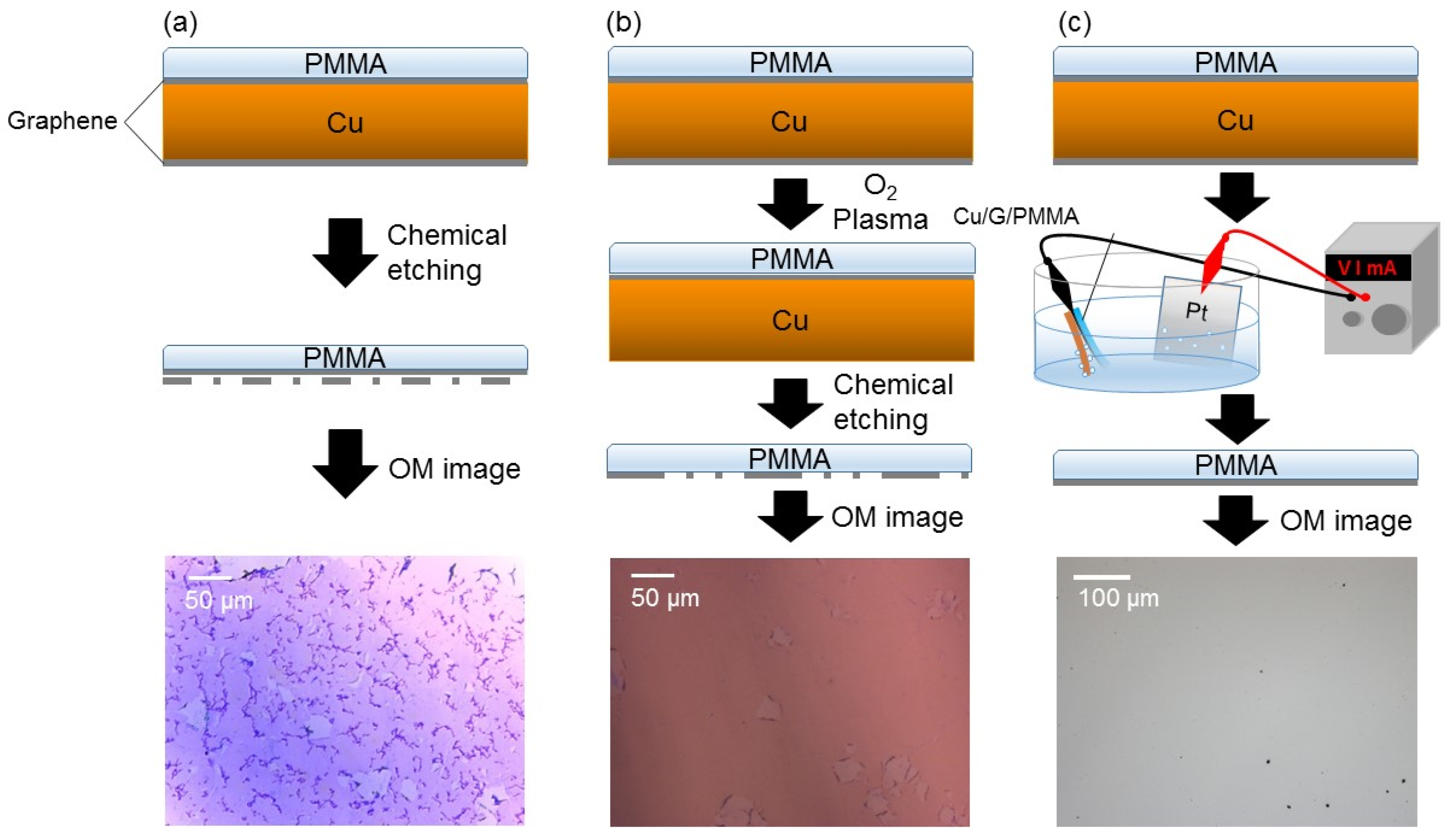
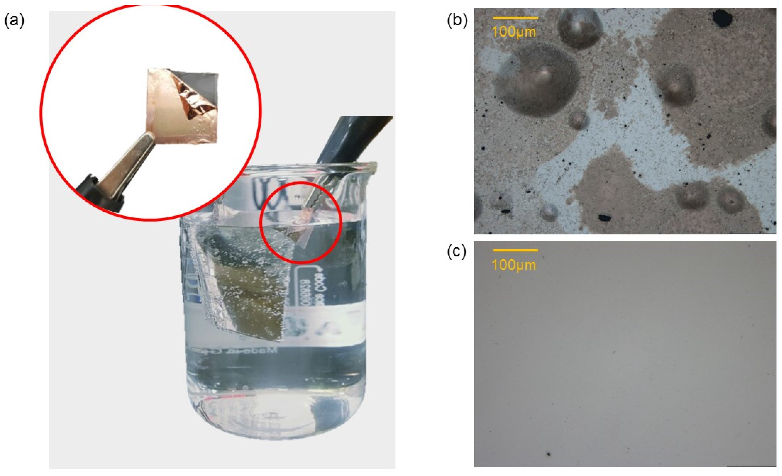
Figure 2.
(a) OM images of graphene on Si/ SiO2 transferred with bubble transfer method; (b) Raman spectrum of graphene made by a Cu foil used for seven cycles of graphene growth and transferred with bubble transfer method.
Figure 2.
(a) OM images of graphene on Si/ SiO2 transferred with bubble transfer method; (b) Raman spectrum of graphene made by a Cu foil used for seven cycles of graphene growth and transferred with bubble transfer method.

Figure 3.
(a) Image of bubble transfer method for Sapphire/Cu and Cu which was detached from sapphire; (b,c) OM images of Sapphire/Cu and Sapphire/Cr/Cu after bubble-transfer.
Figure 3.
(a) Image of bubble transfer method for Sapphire/Cu and Cu which was detached from sapphire; (b,c) OM images of Sapphire/Cu and Sapphire/Cr/Cu after bubble-transfer.

Figure 4.
(a,b) XRD patterns and SEM images of Cu (a) and Cr/Cu (b) before and after CVD; (c) SEM images of Sapphire/Cu before CVD: (1), Sapphire/Cu after CVD (2), Sapphire/Cr/Cu before CVD (3) and Sapphire/Cr/Cu after CVD (4).
Figure 4.
(a,b) XRD patterns and SEM images of Cu (a) and Cr/Cu (b) before and after CVD; (c) SEM images of Sapphire/Cu before CVD: (1), Sapphire/Cu after CVD (2), Sapphire/Cr/Cu before CVD (3) and Sapphire/Cr/Cu after CVD (4).
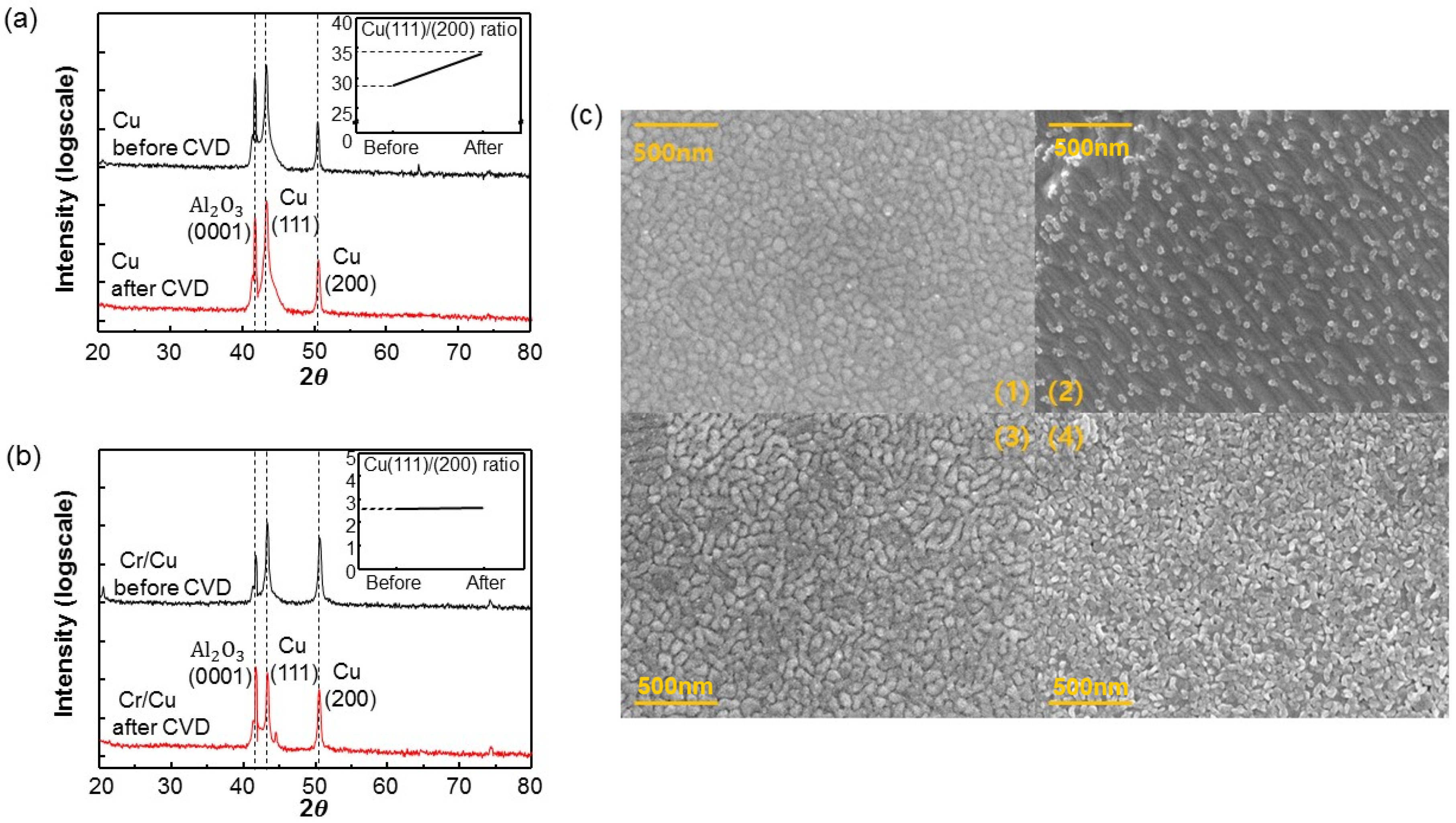
Figure 5.
(a) Cu Cr phase diagram, Raman spectrum of graphene made at 950 °C (b), 970 °C (c).

Table 1.
Mass of the Cu during 7 cycles of CVD process.
| No. of Cycle | 1 | 2 | 3 | 4 | 5 | 6 | 7 |
|---|---|---|---|---|---|---|---|
| Mass of Cu (g) | 0.0235 | 0.0220 | 0.0210 | 0.0198 | 0.0191 | 0.0181 | 0.0171 |
© 2017 by the authors. Licensee MDPI, Basel, Switzerland. This article is an open access article distributed under the terms and conditions of the Creative Commons Attribution (CC BY) license (http://creativecommons.org/licenses/by/4.0/).
Share and Cite
MDPI and ACS Style
Lee, J.; Lee, S.; Yu, H.K. Contamination-Free Graphene Transfer from Cu-Foil and Cu-Thin-Film/Sapphire. Coatings 2017, 7, 218. https://doi.org/10.3390/coatings7120218
AMA Style
Lee J, Lee S, Yu HK. Contamination-Free Graphene Transfer from Cu-Foil and Cu-Thin-Film/Sapphire. Coatings. 2017; 7(12):218. https://doi.org/10.3390/coatings7120218
Chicago/Turabian StyleLee, Jaeyeong, Shinyoung Lee, and Hak Ki Yu. 2017. "Contamination-Free Graphene Transfer from Cu-Foil and Cu-Thin-Film/Sapphire" Coatings 7, no. 12: 218. https://doi.org/10.3390/coatings7120218
Note that from the first issue of 2016, this journal uses article numbers instead of page numbers. See further details here.