
Characterization and Photovoltaic Properties of BiFeO3 Thin Films


Department of Materials Science, The University of Shiga Prefecture, 2500 Hassaka, Hikone, Shiga 522-8533, Japan
*
Author to whom correspondence should be addressed.
Coatings 2016, 6(4), 68; https://doi.org/10.3390/coatings6040068
Submission received: 19 August 2016
/
Revised: 2 December 2016
/
Accepted: 5 December 2016
/
Published: 8 December 2016
(This article belongs to the Special Issue Five Years of Coatings: Coatings Science and Technology for the 21st Century)
Abstract
:Bismuth ferrite (BiFeO3) thin films were prepared by a spin-coating method. Crystal structure and optical properties of the BiFeO3 films were evaluated using X-ray diffraction. The lattice constants, crystallite size, and energy gap of BiFeO3 films depended on the concentration of the BiFeO3 precursor solution. BiFeO3/CH3NH3PbI3 photovoltaic devices were fabricated to investigate photovoltaic properties of BiFeO3. Current density–voltage characteristics of the photovoltaic devices showed rectifying behavior, indicating that BiFeO3 worked as an electron transport layer in CH3NH3PbI3-based photovoltaic devices.
1. Introduction
Bismuth ferrite (BiFeO3) has attracted much attention among researchers, because BiFeO3 is used for potential applications, such as information storage, spintronics, and ferroelectric devices [1,2,3,4,5]. In addition, photovoltaic properties of BiFeO3 bulks, BiFeO3/semiconductor, and BiFeO3/ferroelectric heterostructures have been extensively investigated [6,7,8,9,10,11]. However, photovoltaic properties are sensitive to fabrication process, electronic structure, and interfacial condition. Therefore, precise characterization of BiFeO3 and investigation of BiFeO3-based solar cells are of importance.
Very recently, BiFeO3 films prepared by spin-coating method were used for CH3NH3PbI3-based photovoltaic devices [9]. CH3NH3PbI3 with perovskite structure is known as a fascinating light absorber, and the CH3NH3PbI3-based solar cell is anticipated as a next-generation solar cell [12,13,14,15,16,17,18,19]. BiFeO3 films act as electron transport layers because BiFeO3 is an n-type semiconductor. However, optical and photovoltaic properties of the BiFeO3/CH3NH3PbI3 photovoltaic devices are still unknown.
The purpose of the present work is to characterize BiFeO3 thin films prepared by a simple spin-coating method and investigate photovoltaic properties of BiFeO3/CH3NH3PbI3 photovoltaic devices. The crystal structures of the BiFeO3 thin films prepared from precursor solutions with different concentrations were characterized by X-ray diffraction (XRD). The optical properties of the BiFeO3 films were investigated by collecting optical absorption spectra. The photovoltaic properties of the BiFeO3/CH3NH3PbI3 devices were investigated by measuring current density–voltage (J–V) characteristics and incident photon to current conversion efficiency (IPCE).
2. Materials and Methods
BiFeO3 thin films were prepared on glass substrates by spin-coating method in air atmosphere [20]. Solutions of BiFeO3 with different concentrations were prepared from bismuth nitrate penehydrate (Bi(NO3)3·5H2O) (99.5%, Wako Pure Chemical Industries, Ltd., Osaka, Japan), iron(III) nitrate nonahydrate (Fe(NO3)3·9H2O) (99.0%, Wako Pure Chemical Industries, Ltd.), citric acid (99.5%, Yoneyama Yakuhin Kogyo Co., Ltd., Osaka, Japan), and 2-methoxyethanol (99.0%, 2 mL, Wako Pure Chemical Industries, Ltd.). Citric acid was used as a chelating agent. The concentration of the precursor solution was varied from 0.05 to 0.30 M. Excess 10% Bi(NO3)3·5H2O was added to compensate for Bi loss during annealing. The BiFeO3 solution was dropped on the glass substrate, and was spun at 3000 rpm for 30 s by a spin coater (MS-A100, Mikasa Co., Ltd., Tokyo, Japan). Then, the BiFeO3 precursor film was dried on a hotplate (ND-1, As One Corporation, Osaka, Japan) at 150 °C for 5 min. This process was repeated five times. Finally, the precursor film was annealed in an electric furnace (SMF-1, As One Corporation) at 500 °C for 1 h. Photovoltaic devices with BiFeO3/CH3NH3PbI3 structure were also fabricated by the spin-coating method. Concerning energy level of BiFeO3/CH3NH3PbI3 structure, BiFeO3 and CH3NH3PbI3 are a good combination, because BiFeO3 is an n-type semiconductor [16,21,22]. The fabrication process of the BiFeO3/CH3NH3PbI3 photovoltaic devices is as follows [23]. First, 0.05 M BiFeO3 precursor layer was spin-coated onto a fluorine-doped tin oxide (FTO)-coated glass substrate by the spin-coater at 3000 rpm for 30 s, and was dried onto the hot plate at 150 °C for 5 min. This process was repeated three times. Subsequently, the BiFeO3 layer was annealed in an electric furnace at 500 °C for 30 min. After cooling to room temperature, a 0.10 M BiFeO3 layer was spin-coated onto the 0.05 M BiFeO3 layer at 3000 rpm for 30 s, and was dried onto the hot plate at 150 °C for 5 min. This process was repeated three times. The 0.10 M BiFeO3 layer was annealed in the electric furnace at 500 °C for 2 h. In the present work, a one-step solution deposition method was employed to prepare CH3NH3PbI3 layers [23,24,25,26,27,28,29]. The preparation process was as follows: a mixed solution consisting of methylammonium iodine (CH3NH3I, 98.8 mg, Showa Chemical Co., Ltd., Tokyo, Japan), PbI2 (289.3 mg, Sigma-Aldrich, St. Louis, MO, USA), and γ-butyrolactone (500 μL, Wako Pure Chemical Industries, Ltd.) was prepared by stirring at 60 °C for 2 h in a water bath (BH-22, Masuda Corporation, Osaka, Japan,) attached with a magnetic stirrer (Heracles-20, Koike Precision Instruments, Hyogo, Japan). The CH3NH3PbI3 layer was spin-coated on the BiFeO3 layer at 2000 rpm for 60 s. This process was repeated four times. The spin-coated CH3NH3PbI3 layer was annealed at 100 °C for 15 min. After cooling to room temperature, a hole transport layer was spin-coated on the CH3NH3PbI3 layer at 4000 rpm for 20 s. As the hole transport material, 2,2′,7,7′-tetrakis-(N,N-di-p-methoxyphenylamine)-9,9’-spirobifluorene (spiro-OMeTAD) was used because spiro-OMeTAD can yield higher conversion efficiencies due to its amorphous structure and reasonable hole mobility [30]. The spiro-OMeTAD powder (36.1 mg, Luminescence Technology, Hsinchu City, Taiwan) was dissolved in chlorobenzene (Wako Pure Chemical Industries, Ltd., 500 μL). Solutions of lithium bis(trifluomethylsulfonyl) imide (Li-TFSI, 8.8 μL)and 4-tert-butylpyridine (14.4 μL, Sigma-Aldrich) were added into the spiro-OMeTAD solution. The Li-TFSI solution was prepared by dissolving Li-TFSI powder (260 mg, Tokyo Chemical Industry Co., Ltd., Tokyo, Japan) in acetonitrile (0.5 mL, Wako Pure Chemical Industries, Ltd.). Finally, gold (Au) counter electrodes were thermally deposited on the hole transport layer. For comparison, a photovoltaic device without BiFeO3 layer was fabricated.
The crystal structure of the BiFeO3 thin films was characterized by an X-ray diffractometer (D2 PHASER, Bruker Corporation, Billerica, MA, USA) with CuKα radiation. The film thickness of the BiFeO3 films was checked by atomic force microscopy (AFM) (SPI-3800N/SPA-400, SII Nanotechnology Inc., Chiba, Japan). The optical absorption spectra of the BiFeO3 and CH3NH3PbI3 films were collected using ultraviolet–visible–near-infrared spectrophotometer (V-770, Jasco Corporation, Tokyo, Japan). The J–V characteristics of the photovoltaic devices were recorded using a potentiostat (HSV-110, Hokuto Denko Corporation, Hyogo, Japan). The devices were irradiated under simulated AM 1.5 (100 mW·cm−2) conditions through the bottom of FTO-coated glass substrate by solar simulator (XES-301S, San-Ei Electric Co., Ltd., Osaka, Japan). The effective area of the devices was 0.090 cm2. IPCE spectra of the devices were collected using an IPCE measurement system (QE-R, Enli Technology Co., Ltd., Kaohsiung City, Taiwan). All measurements were performed at room temperature.
3. Results and Discussion
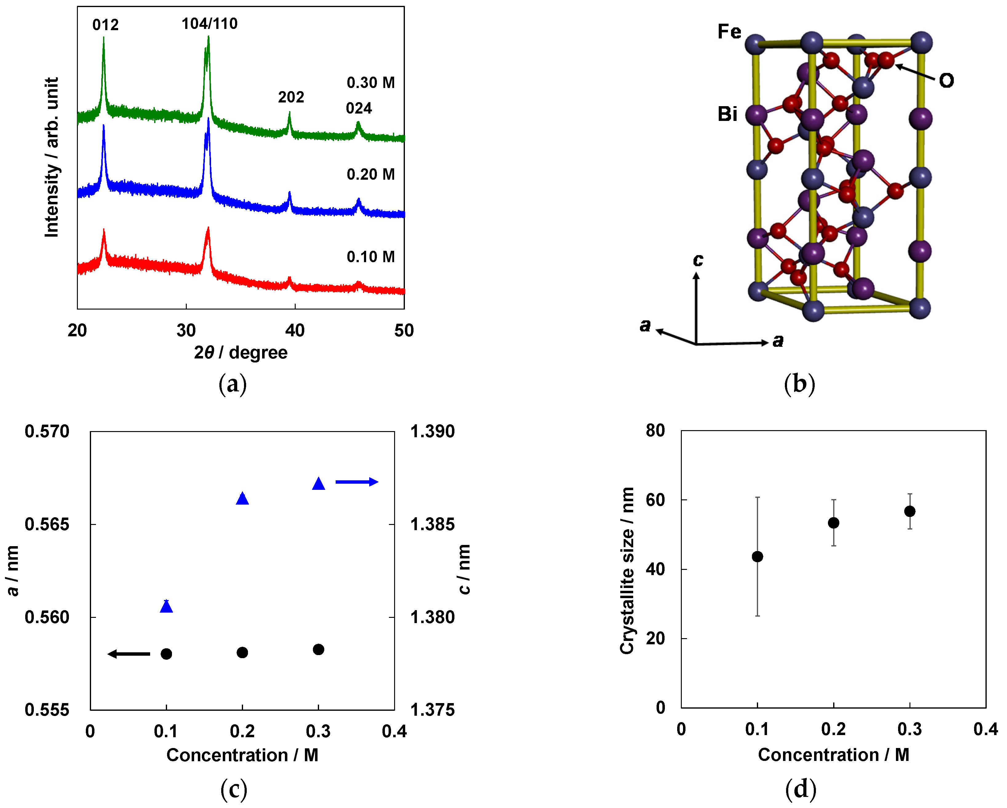
Figure 1a shows XRD patterns of the BiFeO3 thin films. It was confirmed that the BiFeO3 films were polycrystalline with a rhombohedral system. BiFeO3 is usually classed as rhombohedral space group R3c structure with lattice parameter of arh = 0.5634 nm and interaxial angle of αrh = 59.348° [31]. To later discuss lattice distortion in the present BiFeO3 films, the XRD patterns of the BiFeO3 films were indexed on the basis of hexagonal unit cell of BiFeO3, as shown in Figure 1b. Moreover, the film thicknesses of the 0.10 M, 0.20 M, and 0.30 M BiFeO3 films were 224, 336, and 367 nm, respectively; i.e., the film thickness of BiFeO3 films was proportional to the concentration of BiFeO3 precursor solution. This behavior was almost the same as a previous report [32]. The lattice constants of the BiFeO3 were estimated from Equation (1):
Here, a, c, d, and (hkl) are the lattice constants of a- and c-axes, interplanar lattice spacing, and Miller indices, respectively. As shown in Figure 1c, the estimated lattice constants were compatible with those of BiFeO3 bulk [31,33]. On the other hand, the lattice constant of the a-axis slightly increased with increasing concentration of BiFeO3 precursor solution, while that of the c-axis significantly increased at a concentration of 0.20 M. The results suggest that stress in the BiFeO3 films relieved at concentration of 0.20 M. Crystallite sizes (D) of the BiFeO3 were also estimated from the XRD patterns using Scherrer’s equation:
Here, λ, β, and θ are the X-ray wavelength of 0.154184 nm, full width at half maximum of the diffraction peak, and Bragg angle of the diffraction peak, respectively. In the present study, the averaged D values were estimated from D values of 012, 104, and 110 diffraction peaks of the BiFeO3. Figure 1d shows the averaged D of the BiFeO3. The D increased from 42 to 55 nm with increasing concentration of BiFeO3 precursor solution.
D = 0.9λ/βcosθ
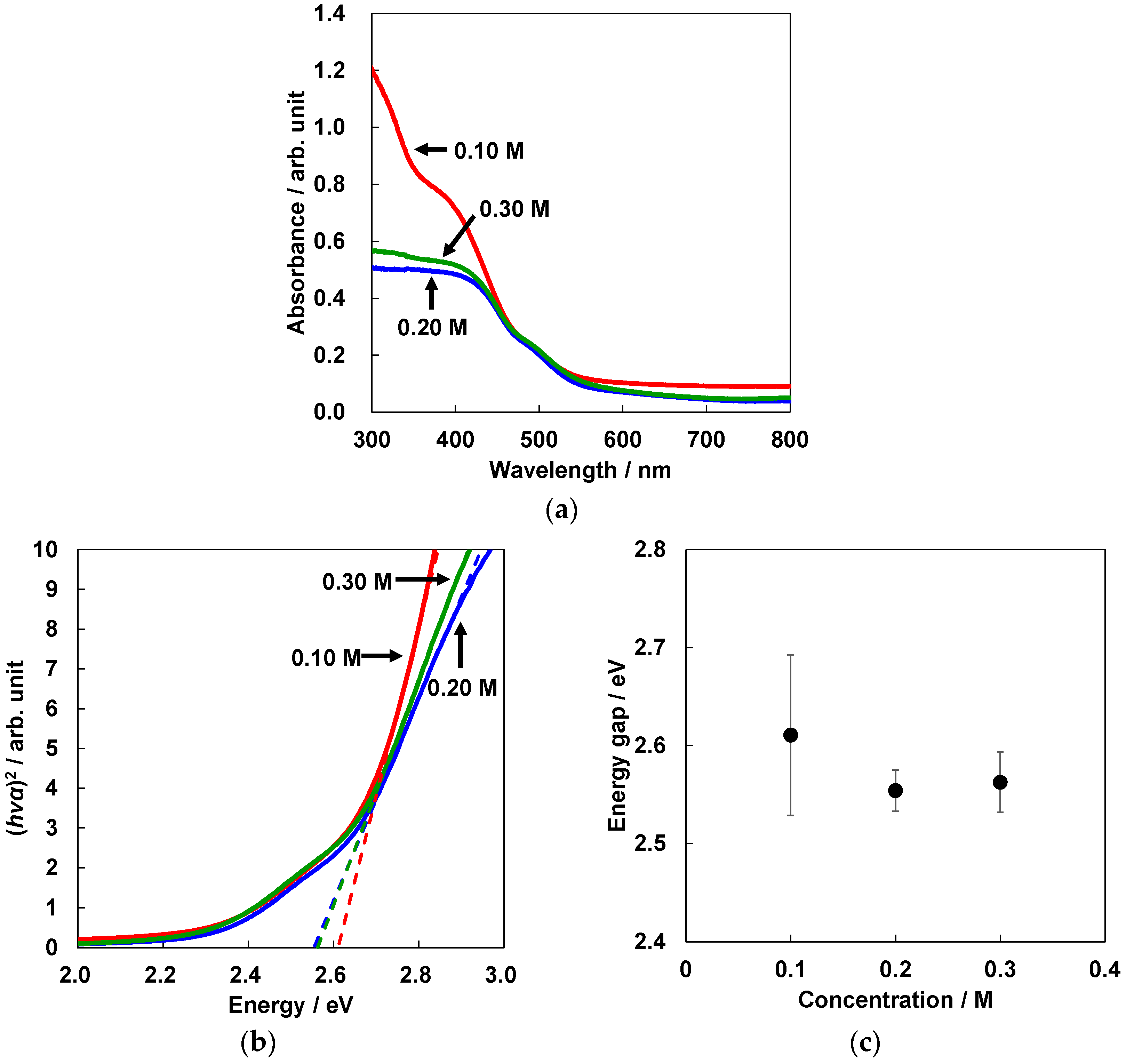
Figure 2a shows optical absorption spectra of the BiFeO3 thin films. The absorption cut-off wavelengths of the films were approximately 565 nm, in agreement with a previous report [34,35,36]. The absorption spectrum of the 0.10 M BiFeO3 film showed a large absorbance in the wavelength from 300 to 450 nm, which is likely associated with lattice distortion in the film. Energy gaps of the BiFeO3 films were calculated by Tauc formula:
Here, h, ν, α, A, Eg, and n are the Plank constant, light frequency, absorption coefficient, proportional constant, energy gap, and power index which depends on the nature of the transition, respectively. In the present study n = 2 was used for the BiFeO3 because BiFeO3 is a direct transition semiconductor [36,37]. The Eg were estimated by extrapolating the linear part of the Tauc plots to meet (hνα)2 = 0, as shown in shown in Figure 2c. The estimated Eg values corresponded to previous reports [6,9,36,37]. On the other hand, the estimated Eg decreased with increasing concentration of BiFeO3 precursor solution, indicating that Eg depended on the concentration of the BiFeO3 solution. Furthermore, the largest Eg was obtained for the 0.10 M BiFeO3 film, which would be a result of lattice distortion in the films.
(hνα)n = A(hν − Eg)
To discuss the lattice distortion in the BiFeO3 films, a simple calculation was attempted using Hooke’s law:
where Δɛ, σ, E are the strain, stress, and Young’s modulus, respectively. In the present study, previously reported Young’s modulus of BiFeO3 was used [39]. The lattice strains for a- and c-axes (Δɛa and Δɛc) are given as follows:
and
Here, a’ and c’ are the lattice constants of BiFeO3 bulk [33]. The calculated σ values for a- and c-axes of BiFeO3 as a function of film thickness are shown in Figure 3. The σ for a-axis slightly increased with increasing film thickness, while that for c-axis significantly increased: the stress for c-axis strongly depended on film thickness. Furthermore, a sign reversal of the σ for c-axis occurred at a film thickness of 367 nm (0.30 M), considering that the 0.10 and 0.20 M BiFeO3 films were wholly under compressive stress, while the 0.30 M BiFeO3 film was partially under tensile stress. Accordingly, a series of variations in crystal structure and optical properties were attributed to compressive stress relaxation in the BiFeO3 films that depended on film thickness.
Δɛ = σ/E
Δɛa = (a’ – a)/a
Δɛc = (c’ – c)/c
Figure 4a shows J–V curves of the FTO/BiFeO3/CH3NH3PbI3/spiro-OMeTAD/Au and FTO/CH3NH3PbI3/spiro-OMeTAD/Au device photovoltaic devices under light irradiation. A clear rectifying behavior was seen for the FTO/BiFeO3/CH3NH3PbI3/spiro-OMeTAD/Au device, while a linear J–V curve was seen for the FTO/CH3NH3PbI3/spiro-OMeTAD/Au one, ensuring that the BiFeO3 acted as an electron transport layer in the present device. From these J–V curves, a short-circuit current density (Jsc) of 0.290 mA cm−2, open-circuit voltage (Voc) of 0.531 V, fill factor (FF) of 0.414, and conversion efficiency (η) of 0.064% were obtained for the FTO/BiFeO3/CH3NH3PbI3/spiro-OMeTAD/Au device. In contrast, a Jsc of 0.652 mA cm−2, Voc of 0.014 V, FF of 0.227, and η of 0.002% were obtained for the FTO/CH3NH3PbI3/spiro-OMeTAD/Au one. However, the η was quite small compared to the previous report [9]. As one of the possible reasons for the low conversion efficiency, external factors such as temperature, humidity, and fabrication process were considered [40]. An IPCE spectrum of the FTO/BiFeO3/CH3NH3PbI3/spiro-OMeTAD/Au photovoltaic device is shown in Figure 4b. The device showed a broad IPCE spectrum in the wavelength range between 320 and 780 nm, indicating that the generation of free electrons and/or free holes occurred in the CH3NH3PbI3 layer under visible light irradiation. An optical absorption spectrum of the same device is also shown in Figure 4b. From the optical absorption spectrum, Eg of the BiFeO3 and CH3NH3PbI3 were estimated to be 2.78 and 1.57 eV, respectively.
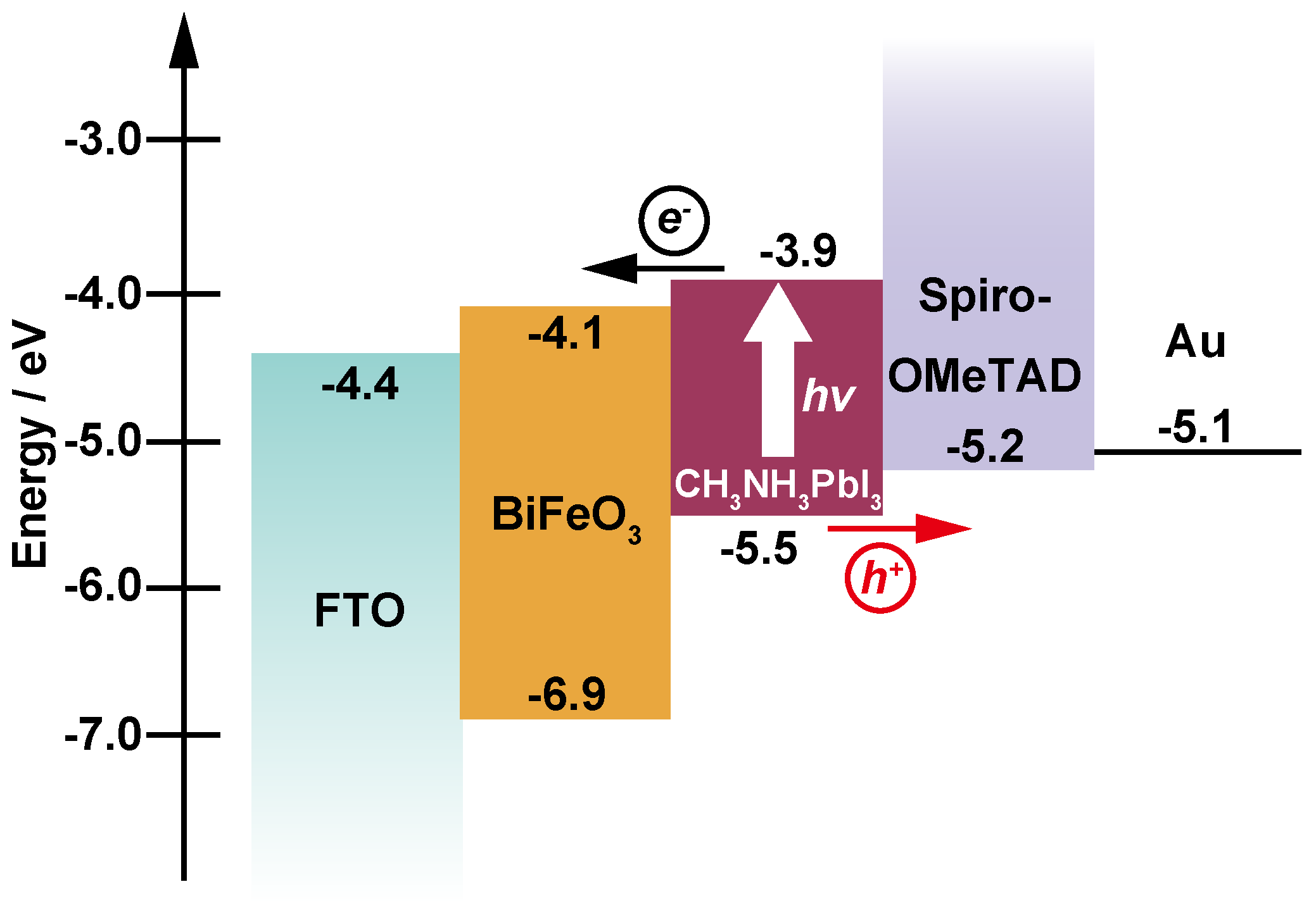
The photovoltaic mechanism based on energy levels is discussed. Figure 5 shows an energy level diagram of the FTO/BiFeO3/CH3NH3PbI3/spiro-OMeTAD/Au photovoltaic device, where previously reported and estimated values were used for the energy levels [16,21,22]. The electronic charge generation occurs in the CH3NH3PbI3 layer by light irradiation from the FTO bottom side. Then, the electrons from the CH3NH3PbI3 are transferred to the FTO electrode through the BiFeO3 electron transport layer. Similarly, the holes are transferred to Au electrode through the spiro-OMeTAD hole transport layer. It has been known that Voc of inorganic/organic solar cells is related to the energy gaps between the conduction band of the inorganic semiconductor and the valence band of the organic semiconductor. According to the energy level diagram in Figure 5, the theoretical Voc of the BiFeO3/CH3NH3PbI3 photovoltaic device can be calculated by the following equation [41]:
Here, e, Ec, EH, and Vloss are the elementary charge, conduction band of inorganic semiconductor, the highest occupied molecular orbital (HOMO) of the organic semiconductor, and the empirical voltage loss for exciton dislocation at a heterojunction, respectively. Usually, the Vloss is 0.3–0.5 V [8,41]. In the present study, the theoretical Voc of the BiFeO3/CH3NH3PbI3 photovoltaic cell was 0.9–1.1 V. These values are greater than the present Voc, as shown in Figure 4a. The obtained low Voc was considered to be due to large Vloss associated with trap states in the CH3NH3PbI3 layer, presumably generated due to partial separation of PbI2 from the CH3NH3PbI3 [23,24,26,27,28]. In addition, it is considered that grains of the present CH3NH3PbI3 were small. In fact, a correlation between grain size and Voc of CH3NH3PbI3-based solar cells was recently reported by Kim et al., and they argued that trap states in CH3NH3PbI3 layer decreased accompanied by enlargement of grains [42]. In our opinion, fabricating a completely pinhole-free CH3NH3PbI3 film is significantly important to achieve high conversion efficiencies. In addition, to avoid deterioration of photovoltaic devices due to many external factors, further development of solar cells that are durable for external factors is required for the improvement of photovoltaic performance.
4. Conclusions
Crystal structures and optical properties of BiFeO3 thin films prepared from precursor solutions with different concentrations were investigated. Polycrystalline BiFeO3 films with a hexagonal system were obtained. The lattice constants, crystallite size, and energy gap of the BiFeO3 films depended on concentration of BiFeO3 precursor solution. The variations in structural parameters and optical properties were attributed to compressive stress relaxation in the BiFeO3 films that depended on film thickness. BiFeO3/CH3NH3PbI3 photovoltaic devices were also fabricated to investigate their photovoltaic properties. The BiFeO3/CH3NH3PbI3 photovoltaic devices showed a rectifying behavior, and a small conversion efficiency was obtained for the present BiFeO3/CH3NH3PbI3 device. From these combined results, BiFeO3 is anticipated as an electron transport layer in solar cells.
Acknowledgments
This work was partly supported by Super Cluster Program of Japan Science and Technology Agency, and Grant-in-Aid for Scientific Research (C) No. 25420760.
Author Contributions
Y.S. and T.O. planned the present study, and wrote the manuscript. Y.S. prepared the samples, and collected the data. T.O. supervised the project.
Conflicts of Interest
The authors declare no conflict of interest.
References
- Kumar, M.M.; Palkar, V.R.; Srinivas, K.; Suryanarayana, S.V. Ferroelectricity in a pure BiFeO3 ceramic. Appl. Phys. Lett. 2000, 76, 2764–2766. [Google Scholar] [CrossRef]
- Wang, J.; Neaton, J.B.; Zheng, H.; Nagarajan, V.; Ogale, S.B.; Liu, B.; Viehland, D.; Vaithyanathan, V.; Schlom, D.G.; Waghmare, U.V.; et al. Epitaxial BiFeO3 multiferroic thin film heterostructures. Science 2003, 299, 1719–2722. [Google Scholar] [CrossRef] [PubMed]
- Zhao, T.; Scholl, A.; Zavaliche, F.; Lee, K.; Barry, M.; Doran, A.; Cruz, M.P.; Chu, Y.H.; Ederer, C.; Spaldin, N.A.; et al. Electrical control of antiferromagnetic domains in multiferroic BiFeO3 films at room temperature. Nat. Mater. 2006, 5, 823–829. [Google Scholar] [CrossRef] [PubMed]
- Allibe, J.; Fusil, S.; Bouzehouane, F.; Daumont, C.; Sando, D.; Jacquet, E.; Deranlot, C.; Bibes, M.; Barthèlèmy, A. Room temperature electrical manipulation of giant magnetoresistance in spin valves exchange-biased with BiFeO3. Nano Lett. 2012, 12, 1141–1145. [Google Scholar] [CrossRef] [PubMed]
- Li, M.; Zhuge, F.; Zhu, X.; Yin, K.; Wang, J.; Liu, Y.; He, C.; Chen, B.; Li, R.-W. Nonvolatile resistive switching in metal/La-doped BiFeO3/Pt sandwiches. Nanotechnology 2010, 21, 425202. [Google Scholar] [CrossRef] [PubMed]
- Choi, T.; Lee, S.; Choi, Y.J.; Kiryukhin, V.; Cheong, S.-W. Switchable ferroelectric diode and photovoltaic effect in BiFeO3. Science 2009, 324, 63–66. [Google Scholar] [CrossRef] [PubMed]
- Sarkar, A.; Khan, G.G.; Chaudhuri, A.; Das, A.; Mandal, K. Multifunctional BiFeO3/TiO2 nano-heterostructure: Photo-ferroelectricity, rectifying transport, and nonvolatile resistive switching property. Appl. Phys. Lett. 2016, 108, 033112. [Google Scholar] [CrossRef]
- Liu, Z.; Yang, F. Photovoltaic effect of BiFeO3/poly(3-hexylthiophene) heterojunction. Phys. Status Solidi RRL 2011, 5, 367–369. [Google Scholar] [CrossRef]
- Zhao, P.; Bian, L.; Wang, L.; Xu, J.; Chang, A. Enhanced open voltage of BiFeO3 polycrystalline film by surface modification of organolead halide perovskite. Appl. Phys. Lett. 2014, 105, 013901. [Google Scholar] [CrossRef]
- Yang, Y.; Xu, W.; Xu, X.; Wang, Y.; Yuan, G.; Wang, Y.; Liu, Z. The enhanced photocurrent of epitaxial BiFeO3 film at 130 °C. J. Appl. Phys. 2016, 119, 044102. [Google Scholar] [CrossRef]
- Chakrabartty, J.; Nechache, R.; Harnagea, C.; Li, S.; Rosei, F. Enhanced photovoltaic properties in bilayer BiFeO3/Bi-Mn-O thin films. Nanotechnology 2016, 27, 215402. [Google Scholar] [CrossRef] [PubMed]
- Kojima, A.; Teshima, K.; Shirai, Y.; Miyasaka, T. Organometal Halide perovskites as visible-light sensitizers for photovoltaic cells. J. Am. Chem. Soc. 2009, 131, 6050–6051. [Google Scholar] [CrossRef] [PubMed]
- Im, J.-H.; Lee, C.-R.; Lee, J.-W.; Park, S.-W.; Park, N.-G. 6.5% efficient perovskite quantum-dot-sensitized solar cell. Nanoscele 2011, 3, 4088–4093. [Google Scholar] [CrossRef] [PubMed]
- Kim, H.-S.; Lee, C.-R.; Im, J.-H.; Lee, K.-B.; Moehl, T.; Marchioro, A.; Moon, S.-J.; Humphry-Baker, R.; Yum, J.-H.; Moser, J.E.; et al. Lead iodide perovskite sensitized all-solid-state submicron thin film mesoscopic solar cell with efficiency exceeding 9%. Sci. Rep. 2012, 2, 591. [Google Scholar] [CrossRef] [PubMed]
- Kim, H.-S.; Lee, L.-W.; Yantara, N.; Boix, P.P.; Kulkarni, S.A.; Mhaisalkar, S.; Grätzel, M.; Park, N.-G. High efficiency solid-state sensitized solar cell-based on submicrometer rutile TiO2 nanorods and CH3NH3PbI3 perovskite sensitizer. Nano Lett. 2013, 13, 2412–2417. [Google Scholar] [CrossRef] [PubMed]
- Zhou, H.; Chen, Q.; Li, G.; Luo, S.; Song, T.-B.; Duan, H.-S.; Hong, Z.; You, J.; Liu, Y.; Yang, Y. Interface engineering of highly efficient perovskite solar cells. Science 2014, 345, 542–546. [Google Scholar] [CrossRef] [PubMed]
- Jeon, N.J.; Noh, J.H.; Yang, W.S.; Kim, Y.C.; Ryu, S.; Seo, J.; Seok, S.I. Compositional engineering of perovskite materials for high-performance solar cells. Nature 2015, 517, 476–480. [Google Scholar] [CrossRef] [PubMed]
- Bi, D.; Yi, C.; Luo, J.; Décoppet, J.-D.; Zhang, F.; Zakeeruddin, S.M.; Li, X.; Hagfeldt, A.; Grätzel, M. Polymer-templated nucleation and crystal growth of perovskite films for solar cells with efficiency greater than 21%. Nat. Energy 2016, 1, 16142. [Google Scholar] [CrossRef]
- Chart of Best Research-Cell Efficiencies provided by National Renewable Energy Laboratory. Available online: http://www.nrel.gov/pv/assets/images/efficiency_chart.jpg (accessed on 2 December 2016).
- Wang, Y.; Jiang, Q.-H.; He, H.-C.; Nan, C.-W. Multiferroic BiFeO3 thin films prepared via a simple sol-gel method. Appl. Phys. Lett. 2006, 88, 142503. [Google Scholar] [CrossRef]
- Wu, F.; Guo, Y.; Zhang, Y.; Duan, H.; Li, H.; Liu, H. Enhanced photovoltaic performance in polycrystalline BiFeO3 thin film/ZnO nanorod heterojunctions. J. Phys. Chem. C 2014, 118, 15200–15206. [Google Scholar] [CrossRef]
- Noh, J.H.; Im, S.H.; Heo, J.H.; Mandal, T.N.; Seok, S.I. Chemical management for colorful, efficient, and stable inorganic-organic hybrid nanostructured solar cells. Nano Lett. 2013, 13, 1764–1769. [Google Scholar] [CrossRef] [PubMed]
- Shirahata, Y.; Suzuki, A.; Oku, T. Fabrication and characterization of bismuth ferrite as an electron transport layer in perovskite photovoltaic devices. J. Ceram. Soc. Jpn. 2016, 124, 602–605. [Google Scholar] [CrossRef]
- Oku, T.; Zushi, M.; Imanishi, Y.; Suzuki, A.; Suzuki, K. Microstructures and photovoltaic properties of perovskite-type CH3NH3PbI3 compounds. Appl. Phys. Express 2014, 7, 121601. [Google Scholar] [CrossRef]
- Zushi, M.; Suzuki, A.; Akiyama, T.; Oku, T. Fabrication and characterization of TiO2/CH3NH3PbI3-based photovoltaic devices. Chem. Lett. 2014, 43, 916–918. [Google Scholar] [CrossRef]
- Suzuki, A.; Okada, H.; Oku, T. Fabrication and characterization of CH3NH3PbI3−x−yBrxCly perovskite solar cells. Energies 2016, 9, 346. [Google Scholar] [CrossRef]
- Oku, T.; Suzuki, K.; Suzuki, A. Effects of chlorine addition to perovskite-type CH3NH3PbI3 photovoltaic devices. J. Ceram. Soc. Jpn. 2016, 124, 234–238. [Google Scholar] [CrossRef]
- Oku, T.; Ohishi, Y.; Suzuki, A. Effects of antimony addition to perovskite-type CH3NH3PbI3 photovoltaic devices. Chem. Lett. 2016, 45, 134–136. [Google Scholar] [CrossRef]
- Ohishi, Y.; Oku, T.; Suzuki, A. Fabrication and characterization of perovskite-based CH3NH3Pb1-xGexI3, CH3NH3Pb1-xTlxI3 and CH3NH3Pb1-xInxI3 photovoltaic devices. AIP Conf. Proc. 2016, 1709, 020020. [Google Scholar]
- Shi, D.; Qin, X.; Li, Y.; He, Y.; Zhong, C.; Pan, J.; Dong, H.; Xu, W.; Li, T.; Hu, W.; Brédas, J.-L.; Bakr, O.M. Spiro-OMeTAD single crystals: Remarkably enhanced charge-carrier transport via mesoscale ordering. Sci. Adv. 2016, 2, e1501491. [Google Scholar] [CrossRef] [PubMed]
- Kubel, H.; Schmid, H. Structure of a ferroelectric and ferroelastic monodomain crystal of the perovskite BiFeO3. Acta Cryst. 1990, B46, 698–702. [Google Scholar] [CrossRef]
- Tang, X.; Dai, J.; Zhu, X.; Yin, L.; Ang, Y.; Song, W.; Yang, Z.; Sun, Y.; Zhang, R. Individual-layer thickness effects on the preferred c-axis-oriented BiFeO3 films by chemical solution deposition. J. Am. Ceram. Soc. 2010, 93, 1682–1687. [Google Scholar]
- Polomska, M.; Kaczmarek, W.; Pająk, Z. Electric and magnetic properties of (Bi1−xLax)FeO3 solid solutions. Phys. Stat. Solidi (a) 1974, 23, 567–574. [Google Scholar] [CrossRef]
- Inorganic Material Database of National Institute for Materials Science. Available online: http://crystdb.nims.go.jp/index_en.html (accessed on 2 December 2016).
- Gao, F.; Chen, X.; Yin, K.; Dong, S.; Ren, Z.; Yuan, F.; Yu, T.; Zou, Z.; Liu, J.-M. Visible-light photocatalytic properties of weak magnetic BiFeO3 nanoparticles. Adv. Mater. 2007, 19, 2889–2892. [Google Scholar] [CrossRef]
- Keskin, V.; Gupta, A.; Szulczewski, G. Solution processed TiO2/BiFeO3/poly(3-hexylthiophene) solar cells. Mater. Lett. 2015, 159, 305–308. [Google Scholar] [CrossRef]
- Sun, Y.; Liu, Z.; Zeng, J.; Yan, J.; Shi, D.; Liu, H. Photovoltaic effects in polarized polycrystalline BiFeO3 films. J. Electron. Mater. 2015, 44, 4207–4212. [Google Scholar] [CrossRef]
- Xu, X.; Lin, Y.-H.; Li, P.; Shu, L.; Nan, C.-W. Synthesis and photocatalytic behaviors of high surface area BiFeO3 thin films. J. Am. Ceram. Soc. 2011, 94, 2296–2299. [Google Scholar] [CrossRef]
- Sen, P.; Dey, A.; Mukhopadhyay, A.K.; Bandyopadhyay, S.K.; Himanshu, A.K. Nano indentation behaviour of nano BiFeO3. Ceram. Int. 2012, 38, 1347–1352. [Google Scholar] [CrossRef]
- Zhao, X.; Park, N.-G. Stability issues on perovskite solar cells. Photonics 2015, 2, 1139–1151. [Google Scholar] [CrossRef]
- Scharber, M.C.; Mühlbacher, D.; Koppe, M.; Denk, P.; Waldauf, C.; Heeger, A.J.; Brabec, C. Design rules for donors in bulk-heterojunction solar cells—Towards 10 % energy-conversion efficiency. Adv. Mater. 2006, 18, 789–794. [Google Scholar] [CrossRef]
- Kim, H.D.; Ohkita, H.; Benten, H.; Ito, S. Photovoltaic performance of Perovskite Solar Cells with Different Grain Sizes. Adv. Mater. 2016, 28, 917–922. [Google Scholar] [CrossRef] [PubMed]
Figure 1.
(a) X-ray diffraction (XRD) patterns of BiFeO3 thin films grown on glass substrates; (b) Schematic illustration of hexagonal unit cell of BiFeO3; (c) Lattice constants and (d) crystallite sizes of BiFeO3 as a function of concentration of BiFeO3 precursor solution. The crystallographic information data of (b) was downloaded from Ref. [38].

Figure 2.
(a) Optical absorption spectra of BiFeO3 thin films grown on glass substrates; (b) Tauc plots of BiFeO3 films; (c) Energy gaps of BiFeO3 films as a function of concentration of the BiFeO3 precursor solution.
Figure 2.
(a) Optical absorption spectra of BiFeO3 thin films grown on glass substrates; (b) Tauc plots of BiFeO3 films; (c) Energy gaps of BiFeO3 films as a function of concentration of the BiFeO3 precursor solution.

Figure 3.
Stresses along a- (filled circle) and c-axes (filled triangle) of BiFeO3 as a function of film thickness of BiFeO3.
Figure 3.
Stresses along a- (filled circle) and c-axes (filled triangle) of BiFeO3 as a function of film thickness of BiFeO3.
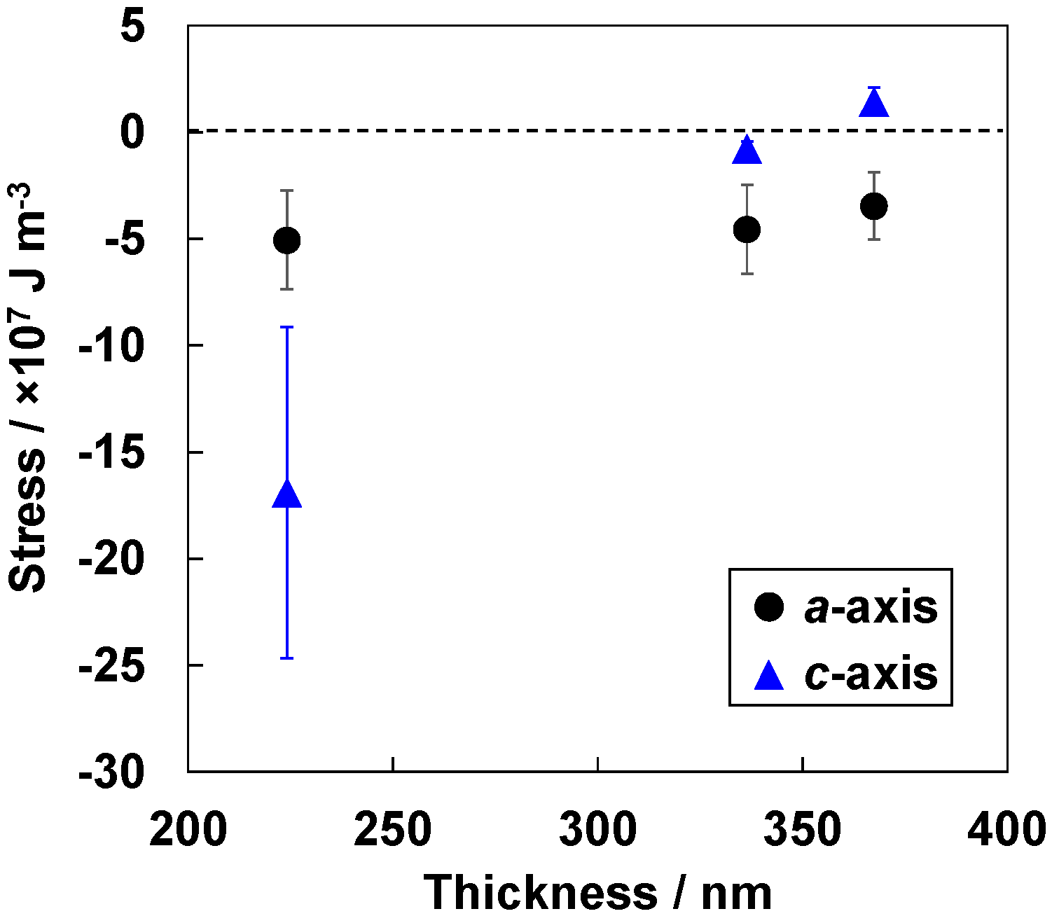
Figure 4.
(a) J–V curves of FTO/BiFeO3/CH3NH3PbI3/spiro-OMeTAD/Au (w/ BiFeO3) and FTO/CH3NH3PbI3/spiro-OMeTAD/Au (w/o BiFeO3) devices; (b) Incident photon to current conversion efficiency (IPCE) (left) and optical absorption spectra (right) of FTO/BiFeO3/CH3NH3PbI3/spiro-OMeTAD/Au device. FTO: fluorine-doped tin oxide; Spiro-OMeTAD: 2,2’,7,7’-tetrakis-(N,N-di-p-methoxyphenylamine)-9,9’-spirobifluorene.
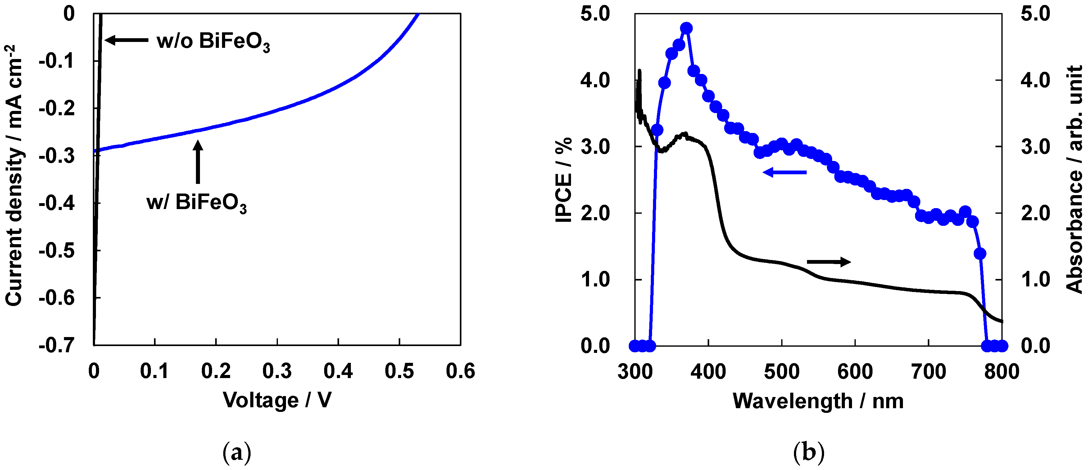
Figure 5.
Energy level diagram of FTO/BiFeO3/CH3NH3PbI3/spiro-OMeTAD/Au photovoltaic device.
© 2016 by the authors; licensee MDPI, Basel, Switzerland. This article is an open access article distributed under the terms and conditions of the Creative Commons Attribution (CC-BY) license (http://creativecommons.org/licenses/by/4.0/).
Share and Cite
MDPI and ACS Style
Shirahata, Y.; Oku, T. Characterization and Photovoltaic Properties of BiFeO3 Thin Films. Coatings 2016, 6, 68. https://doi.org/10.3390/coatings6040068
AMA Style
Shirahata Y, Oku T. Characterization and Photovoltaic Properties of BiFeO3 Thin Films. Coatings. 2016; 6(4):68. https://doi.org/10.3390/coatings6040068
Chicago/Turabian StyleShirahata, Yasuhiro, and Takeo Oku. 2016. "Characterization and Photovoltaic Properties of BiFeO3 Thin Films" Coatings 6, no. 4: 68. https://doi.org/10.3390/coatings6040068
Note that from the first issue of 2016, this journal uses article numbers instead of page numbers. See further details here.