Article

Fundamental Study on the Effect of Spray Parameters on Characteristics of P3HT:PCBM Active Layers Made by Spray Coating

University of Michigan-Shanghai Jiao Tong University Joint Institute, Shanghai 200240, China
*
Author to whom correspondence should be addressed.
Coatings 2015, 5(3), 488-510; https://doi.org/10.3390/coatings5030488
Submission received: 6 July 2015 / Revised: 5 August 2015 / Accepted: 12 August 2015 / Published: 19 August 2015

Abstract

:
This paper is an attempt to elucidate the effects of the important spray characteristics on the surface morphology and light absorbance of spray-on P3HT:PCBM thin-films, used as an active layer in polymer solar cells (PSCs). Spray coating or deposition is a viable scalable technique for the large-scale, fast, and low-cost fabrication of solution-processed solar cells, and has been widely used for device fabrication, although the fundamental understanding of the underlying and controlling parameters, such as spray characteristics, droplet dynamics, and surface wettability, is still limited, making the results on device fabrication not reproducible and unreliable. In this paper, following the conventional PSC architecture, a PEDOT:PSS layer is first spin-coated on glass substrates, followed by the deposition of P3HT:PCBM using an automatic ultrasonic spray coating system, with a movable nozzle tip, to mimic an industrial manufacturing process. To gain insight, the effects of the spray carrier air pressure, the number of spray passes, the precursor flow rate, and precursor concentration are studied on the surface topography and light absorbance spectra of the spray-on films. Among the results, it is found that despite the high roughness of spray-on films, the light absorbance of the film is satisfactory. It is also found that the absorbance of spray-on films is a linear function of the number of spray passes or deposition layers, based on which an effective film thickness is defined for rough spray-on films. The effective thickness of a rough spray-on P3HT:PCBM film was found to be one-quarter of that of a flat film predicted by a simple mass balance.

1. Introduction

Emerging solution-processed thin-film solar cells, such as polymer solar cells (PSCs) and perovskite solar cells, are promising alternatives to silicon-based and inorganic thin-film solar cells, due to their potential for low-cost and vacuum-free fabrication from solution, device transparency, and mechanical flexibility [1,2,3]. Their drawbacks including the lack of a reliable scalable manufacturing technique, and low device stability and lifetime, which are yet to be addressed.
The donor/acceptor (D/A) components of the active layer of a PSC are well mixed together, making a bulk heterojunction (BHJ) layer [4,5]. The standard and widely studied D/A system used in PSCs is the P3HT:PCBM blend, where P3HT (poly(3-hexylthiophene-2,5-diyl) and PCBM (phenyl-C61-butyric acid methyl ester), respectively, work as the donor and acceptor in the conventional cell architecture of glass/ITO/PEDOT:PSS/P3HT:PCBM/Al, where ITO (indium tin oxide) is a transparent electrode, and PEDOT:PSS (poly(3,4-ethylenedioxythiophene):poly(styrenesulfonic acid)) is an electron-blocking layer. Compared with the other D/A systems with a higher power conversion efficiency (PCE), P3HT:PCBM is more desirable for research purposes, given that it has been widely studied, and thus is selected in this study to investigate its deposition behavior by ultrasonic spray coating. The results may be generalized to other similar D/A systems as well.
Spin coating is a widely used lab-scale and simple method for the fabrication of most layers of PSCs and other solution-processed solar cell layers because it can produce hole-free, intact, and uniform thin films. The improvement of the spun-on PSCs with a P3HT:PCBM layer as the active layer is performed through adjusting the nano-structure of the P3HT:PCBM blend for better exciton generation, dissociation, and transport, where the film thickness is mostly controlled by the rotation speed and spinning duration. For instance, the effect of the thickness of P3HT:PCBM film on the PCE was studied by Li et al. [6] by examining the film thickness ranging from 35 nm to 155 nm. It was found that the highest PCE of 4% occurs at the film thickness of 63 nm. Later, however, devices with thicker active layers were fabricated. For example, Zeng et al. [7] examined the thickness in the range of 130 nm to 1200 nm and found that the device short circuit current decreases with increasing the film thickness, if no thermal annealing applies, while the thermal annealing recovers the efficiency loss caused by an increase in thickness. Therefore, the thick-layer devices (beyond 300 nm) may have better performances than those devices with thinner active layers and, importantly, the sensitivity of efficiency to thickness in thick-layer devices is less than the sensitivity in thin-layer devices. This implies that the performance of a PSC device is a function of thickness, and more importantly, a function of the film nano-structure (charge transfer pathways). Thus, to study the effect of thickness on the performance, one needs to ensure that as the thickness changes, the nano-structure remains unchanged, something which is difficult to achieve. Mathematical models correlating the process parameters, such as rotation speed and film thickness, have been established [8,9,10,11,12]. These models will be used and discussed later in this paper. It has been claimed that using thermal annealing [13,14,15] and solvent treatment [16,17], the efficiency of the conventional PSCs consisting of glass/ITO/PEDOT:PSS/P3HT:PCBM/Al can increase to 5%. A PCE of 6% for a P3HT:PCBM-based PSC has been reported as well [18], although those high values in efficiency were questioned [19]. Undoubtedly, the optimized nano-structure of the D/A network favors the device performance allowing electrons and holes to find their ways to the cathode and anode, respectively.
While spin coating is a simple, low-cost, and controllable method for the fabrication of thin films from a solution, its applicability is limited to lab-scale research and development purposes, and thus it is not suitable for the mass production of SCs. Only some of the knowledge gained by the fundamental studies on a particular fabrication method may be transferable to another. Therefore, fundamental studies on the fabrication of various layers by scalable methods, such as spray coating, are essential for the sustainable development and commercialization of such emerging solar cells. Our research focuses on spray coating, which is believed to be one of the most viable scalable techniques for this purpose. During spray coating, using an atomization technique, such as ultrasonic or air-assist atomization, a precursor solution is atomized into spray droplets at the nozzle tip, where the spray droplets are carried to the substrate placed at a distance from the nozzle tip. The nozzle tip and/or the substrate usually move with respect to one another to allow uniform deposition of the precursor solution, making spray coating a roll-to-roll compatible process if flexible substrates are used. Compared to other widely reported scalable methods for the fabrication of PSCs, such as screen printing [20], inkjet printing [21], and slot-die printing [22], spray coating is a fast, high-throughput fabrication method and is capable of fabricating thin films with nano-scale thickness, which is required for the efficient performance of some layers [3,23,24,25]. Even a fully spray-processed solar cell has been fabricated in air [24].
Gaining an in-depth understanding of the spray coating process for solar cell materials entails further research, which is the objective of this work. While spray coating has been widely employed to fabricate some layers of PSCs, such as P3HT: PCBM, minimum information has been provided on the details of the spray coating process; in other words, the spray coating process itself has been treated as a black box. The PCEs of spray-on devices based on P3HT: PCBM are usually around 2%–3%, lower than those of devices made by spin coating [26,27,28,29,30,31,32,33,34,35,36,37]. This is because, the typical spray-on films are not uniform and under unfavorable spraying conditions may consist of stacks of dried solution droplets or so-called splats [26,27,28,30,31,32,33,34,35,36,37,38]. Also, the lower PCEs of the spray-on devices may be attributed to excessive roughness, although the device performance is seemingly more related to the film nano-structure, which requires adequate process understanding and controlling. Recently, we have studied the surface topography, structure, and electrical conductivity of spray-on PEDOT:PSS layers [23,39], where the effects of the substrate temperature, the number of spray passes, and the imposing substrate vibration on the morphology and functionality of PEDOT:PSS were explored. It was found that employing multiple spray passes improves the coverage and the electrical conductivity of PEDOT:PSS films. In this study, we explore the characteristics of the P3HT:PCBM active layer fabricated by spray coating, and also spin coating for comparison. Confocal laser scanning microscopy (CLSM) is used as the main characterization tool for surface topography. The light absorbance of the films is also obtained. This systematic study will provide insight into the optimum conditions for spray coating and the relationship between the spray characteristics and the film morphology relevant to the photovoltaic performance of a PSC.

2. Experimental Methods

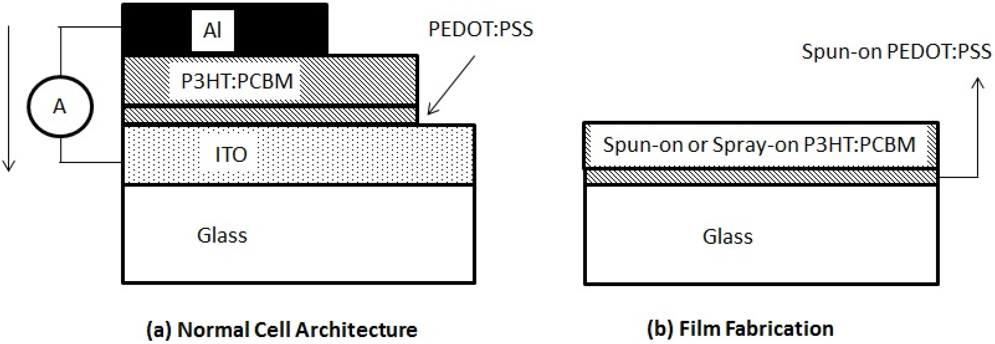
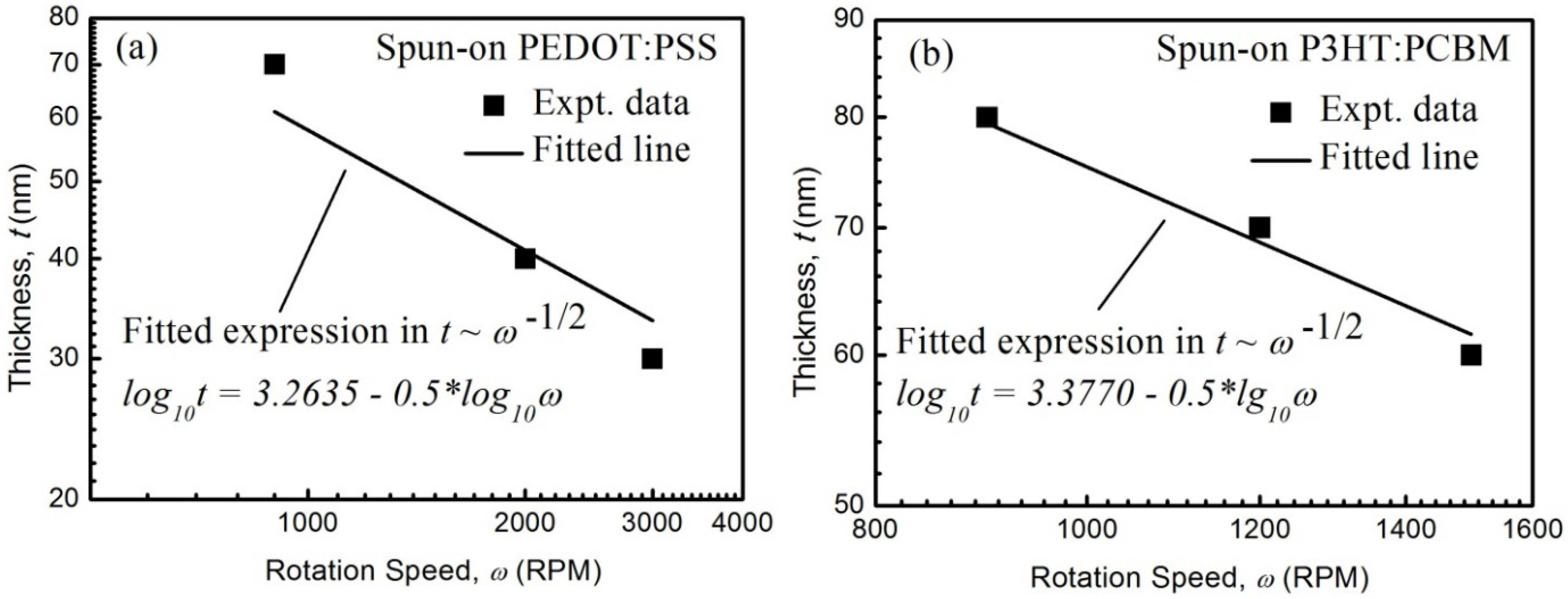
2.1. Fabrication of Spun-On PEDOT:PSS and P3HT:PCBM Films

Figure 1a shows the schematic of a conventional PSC, i.e., glass/ITO/PEDOT:PSS/P3HT: PCBM/Al architecture. A P3HT:PCBM film was deposited on spun-on PEDOT:PSS film by both spin and spray coating methods. Since in this work the fabrication and photovoltaic test of an entire device is not concerned, the PEDOT:PSS film was deposited on bare glass rather than the ITO-coated glass, as shown in Figure 1b. The PEDOT:PSS aqueous solution purchased from Sigma-Aldrich with 1.3 wt % of PEDOT:PSS (0.5% PEDOT:0.8% PSS) dispersed in water was used as-received. The PEDOT:PSS molecular weight was measured to be 65227 g/mol using Gel Permeation Chromatography (PDA model, Shimadzu Scientific Instruments, INC., Kyoto, Japan). Before spin coating, the 24 mm × 24 mm bare glass substrates were cleaned in an ultrasonic bath using detergent, deionized water, and isopropanol, in sequence, for 15 min each. The spun-on films were then cured in an oven at the temperature of 120 °C for 30 min.
Figure 1. (a) Conventional PSC architecture, and (b) film fabrication sequence followed in the experiments, in which first a PEDOT:PSS film was fabricated by spin coating, followed by deposition of a layer of P3HT:PCBM on top, by spin and spray coating.
Coatings 05 00488 g001
P3HT and PCBM powders were purchased from J&K Scientific, China, and used as-received. The P3HT and PCBM in a weight ratio of 1:0.8 were mixed and dissolved in chlorobenzene (CB) to make a solution with the concentration of 18 mg/mL for spin coating, and diluted to 1.8, 0.9, 0.36 mg/mL for spray coating experiments. Before deposition, the solution was stirred overnight and filtered using a 0.3 μm filter. Various rotation speeds were examined, where the thickness (t) of the P3HT:PCBM film was found dependent on the rotation speed (w) in the form of t ~ w−0.5 with details provided in Section 3.1.

2.2. Fabrication of Spray-On P3HT:PCBM Films

The ultrasonic atomization spraying equipment (Holmarc Opto-Mechatronics Pvt. Ltd., Model HO-TH-04, Kerala, India) was used to deposit P3HT:PCBM films on spun-on PEDOT:PSS films, as shown in Figure 1b. For spray coating experiments, the P3HT and PCBM were mixed in a ratio of 1:0.8 and dissolved into CB solvent, similar to spin coating experiments but here, to avoid nozzle clogging, diluter solutions with concentrations of 1.8, 0.9, 0.36 mg/mL were used compared to the concentration of 18 mg/mL used for spin coating. For dilute solutions, multiple spray passes were used to achieve desired thickness and performance. Being able to use dilute solutions during film fabrication is one of the advantages of spray coating compared to spin coating to address the low solubility problem of solar cell materials in non-toxic solvents. For instance, Ishikawa et al. [38] fabricated the active layer of a solar cell using spray deposition utilizing an ultra-dilute solution with the concentration of 1 ppm.
During the spray deposition process, P3HT:PCBM solution was atomized into tiny droplets at the ultrasonic nozzle tip, and carried to the substrate with the aid of compressed air at various pressures. The air velocity is not known at each air pressure. However, given that the role of air is to carry the ultrasonically atomized droplets to the substrate, and not to atomize the liquid, the air velocity is smaller than that in air-assist nozzles, and is estimated to be within 1–10 m/s. Using high-frequency vibrations, ultrasonic nozzles create a mist of micron-sized droplets that can impinge on the substrate without bouncing back. The precursor solution is stored in a mechanically pressurized container using a piston. The precursor solution is pumped to the ultrasonic nozzle (inner diameter of 200 μm). The precursor solution flow rate is controlled by the motion of the piston. In the operational frequency of the ultrasonic nozzle used (40 kHz), the droplet size at the nozzle tip is about 50 μm. The solvent evaporates slightly during droplet flight and substantially after arrival on the (heated) substrate, leaving behind a thin solid film [40]. Details of the apparatus and its components may be found elsewhere [23,39].
The process parameters, including (1) the precursor flow rate, (2) carrier air pressure, (3) nozzle tip and substrate distance, (4) substrate temperature, (5) traveling speed of the nozzle tip, and (6) deposition time, and the number and sequence of spray passes, could be varied manually or through programming. In our experiments, the effects of varying the carrier air pressure, the number of spray passes, the precursor flow rate, and the concentration on the characteristics of spray-on P3HT:PCBM films were studied and other parameters were kept constant. The process parameters used in this experiment are listed in Table 1.
Table 1. Process parameters in spray coating.
Parameter (Unit)Value
Precursor solution flow rate (mL/min)1, 2, 5
Precursor solution concentration (mg/mL)1.8, 0.9, 0.36
Nozzle tip to substrate distance (cm)9
Substrate temperature (°C)55
Nozzle tip moving speed in (x, y) direction (mm/s) (10, 0)
Nozzle moving distance (x, y) in one round (mm) 40
Air pressure (MPa)0.1, 0.2, 0.3 or 0.4
Number of spray deposition passes 1, 15, 30

2.3. Characterization

The fabricated films were characterized by a confocal laser scanning microscope (CLSM 700, ZEISS, Oberkochen, Germany), using both laser and optical modes to visualize surface topography and to identify surface uniformity, roughness, and defects. Confocal laser scanning microscopy (CLSM) uses the confocal technique [41] to obtain three-dimensional (3D) images and has been first applied to biological samples [42,43]. A pinhole is located at the confocal plane of the lens to allow only the in-focus light to pass, which improves the spatial resolution by eliminating the out-of-focus light. The image of a surface plane at a certain thickness is synthesized by scanning the plane, point by point, and then a three-dimensional image is obtained by constructing those images for different depths.
Usually, the atomic force microscopy (AFM) is used for surface characterization because of its high vertical resolution in the range of 0.1 nm, but AFM is a slow process and its field of view is rather small, not enough for spray-on films, and is generally composed of splat sizes ranging from 10 to several hundred micrometres. AFM images would only scan a small portion of the film, perhaps within a single splat. The CLSM is a touch-free and non-destructive characterization tool with a wide field of view and it is capable of providing optical and laser images in two dimensions and three dimensions. Also, the CLSM is a fast-scanning and low-maintenance method with no moving parts. Thus, the CLSM was found adequate and effective and can be used in solar cell research. There are other surface characterization techniques as well, such as stylus profilometry and optical interferometry, each with its advantages and disadvantages.
The accuracy and adequacy of the CLSM for film characterization will be evaluated first, given that few studies have employed the CLSM as a nano-scale characterization tool (cf. Section 3.1). During characterization, three scratches were made on a film to expose the substrate surface; the glass is hard enough while the polymer film is soft and easily removed. The point or local thickness could then be obtained by measuring the height difference between two points located on the film surface and scratched surface. In addition, film roughness was obtained along selected lines. To validate the accuracy of the CLSM thickness measurements, an Atomic Force Microscope (AFM, model Dimension 3100, Veeco Instruments, Inc., Plainview, NY, USA) was used to characterize selected samples. For both AFM and CLSM measurements, square areas of 10 μm × 10 μm were selected for surface roughness measurements on spun-on PEDOT:PSS films. The UV-Visible light absorption spectra of P3HT:PCBM films were obtained using UV-Visible spectrophotometry (EV300, Thermo Fisher Scientific, Waltham, MA, USA). The scanning step was set at 1 nm.
The equilibrium contact angle of sessile solution droplets on the substrates were measured using an optical contact angle instrument system (Dataphysics, model OCA 15, Filderstadt, Germany). A single solution droplet was injected from a syringe (internal diameter of 0.7 mm).

3. Results and Discussion

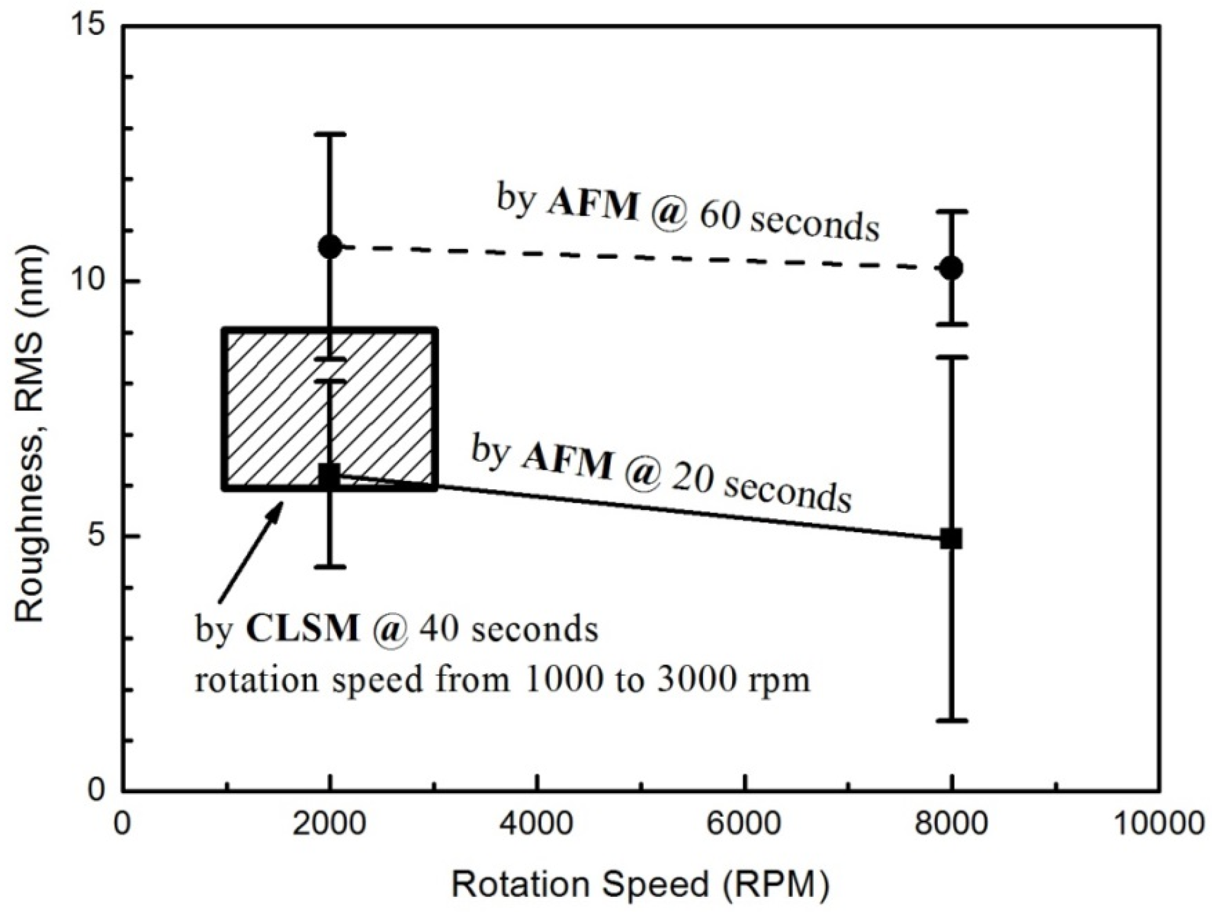
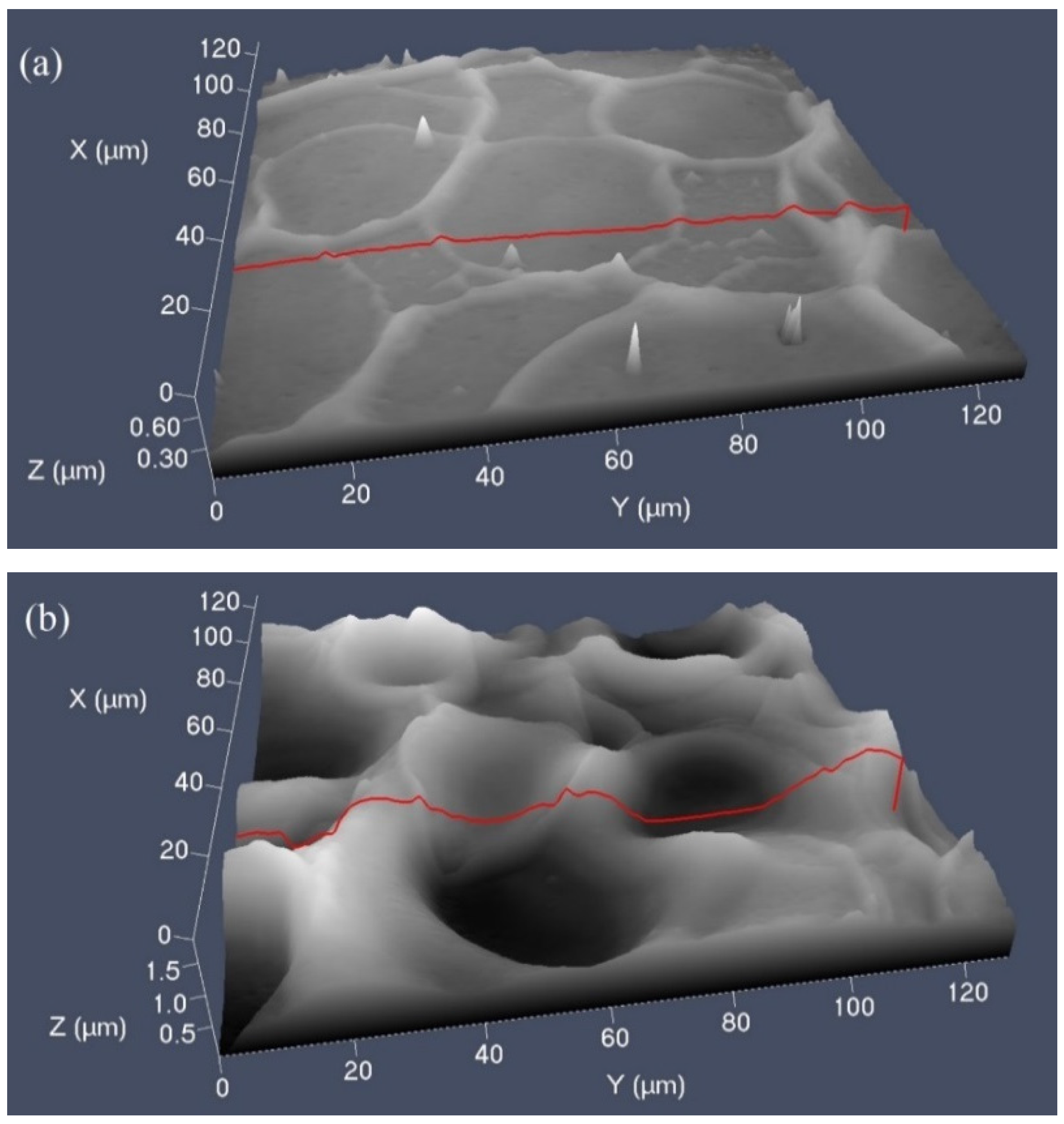
3.1. Accuracy of the CLSM Measurements

Figure 2 shows the root mean squared (RMS) surface roughness of spun-on PEDOT:PSS films measured by AFM and CLSM in the same field of view of 10 μm × 10 μm. The AFM-measured roughness lines show that film roughness increases with increasing the spinning duration time, so it is rational to observe that the roughness of the films fabricated at the spinning duration time of 40s, measured by the CLSM, which falls between the two AFM lines. The AFM results also show that the roughness does not change significantly with the rotation speed if the error bar is considered. Therefore, the comparison between the AFM and CLSM results show that the CLSM has sufficient resolution to characterize the thin films in nano-scale.
Figure 2. Surface roughness values of spun-on PEDOT:PSS films obtained by AFM in the form of solid symbols with error bars. Also shown is the roughness of spun-on films made at 1000, 2000, and 3000 RPM at 40 s spinning time, measured by CLSM (the hatched rectangle). The CLSM-measured roughness values fall within the two AFM-measured roughness lines, as shown in the graph, showing the adequate accuracy of the CLSM measurements. Field of view for surface roughness measurements is 10 μm × 10 μm.
Coatings 05 00488 g002
Figure 3 shows the thickness vs. rotation speed of spun-on PEDOT:PSS and P3HT:PCBM films. Thin film thickness has been well related to the spin coating process parameters through both experimental and theoretical works [8,9,10,11,12]. The simplest model was developed in 1984 [8] but found inaccurate for ultra-thin films (<200 nm) [10]. After considering more factors, a more complex and accurate model has been proposed for ultra-thin films [10]. Despite the differences between modeling thin and ultra-thin films, both share a basic concept in that the deposited film thickness (t) is proportional to the rotation velocity (w) as t ~ w−0.5. It has been proven that this expression holds even when the thickness is as small as few nanometers [10,12]. To be able to estimate the thickness of ultra-thin films, the appearance of the short range intermolecular forces between the film and the interfaces, when the thickness is less than 30 nm, has to be taken into consideration, which is a formidable task [11]. Here, we fitted the film thickness data points obtained by the CLSM, using the least squares method (cf. Figure 3) with an acceptable coefficient of determination (R2), as shown in the caption of Figure 3. It can be seen that the measured data can be fitted well by the expression relating the thickness to the rotation speed in the form of t ~ w−0.5, as expected, demonstrating again that the CLSM is a viable film characterization tool in the nanometer scale, and thus the CLSM is used to characterize the spray-on films in the rest of this paper.
Figure 3. Measured spun-on film thickness by CLSM vs. rotation speed (solid square symbols) and fitting line based on the least squares method; (a) PEDOT: PSS film and (b) P3HT: PCBM film. The figure is in log-log scale. The R2 in (a) is 0.9 and in (b) is 0.99.
Coatings 05 00488 g003

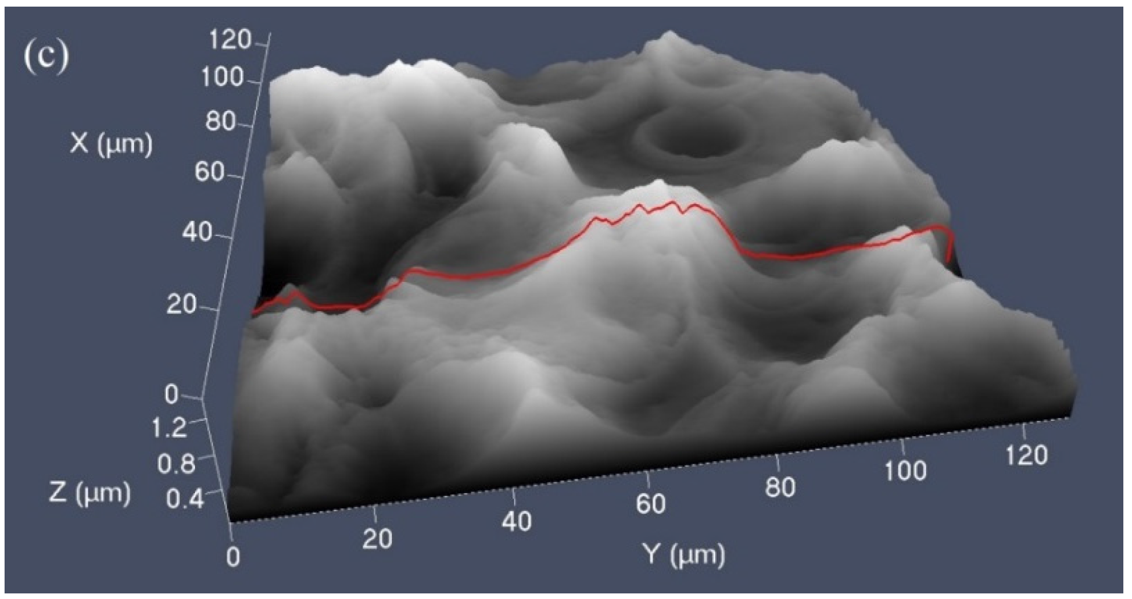
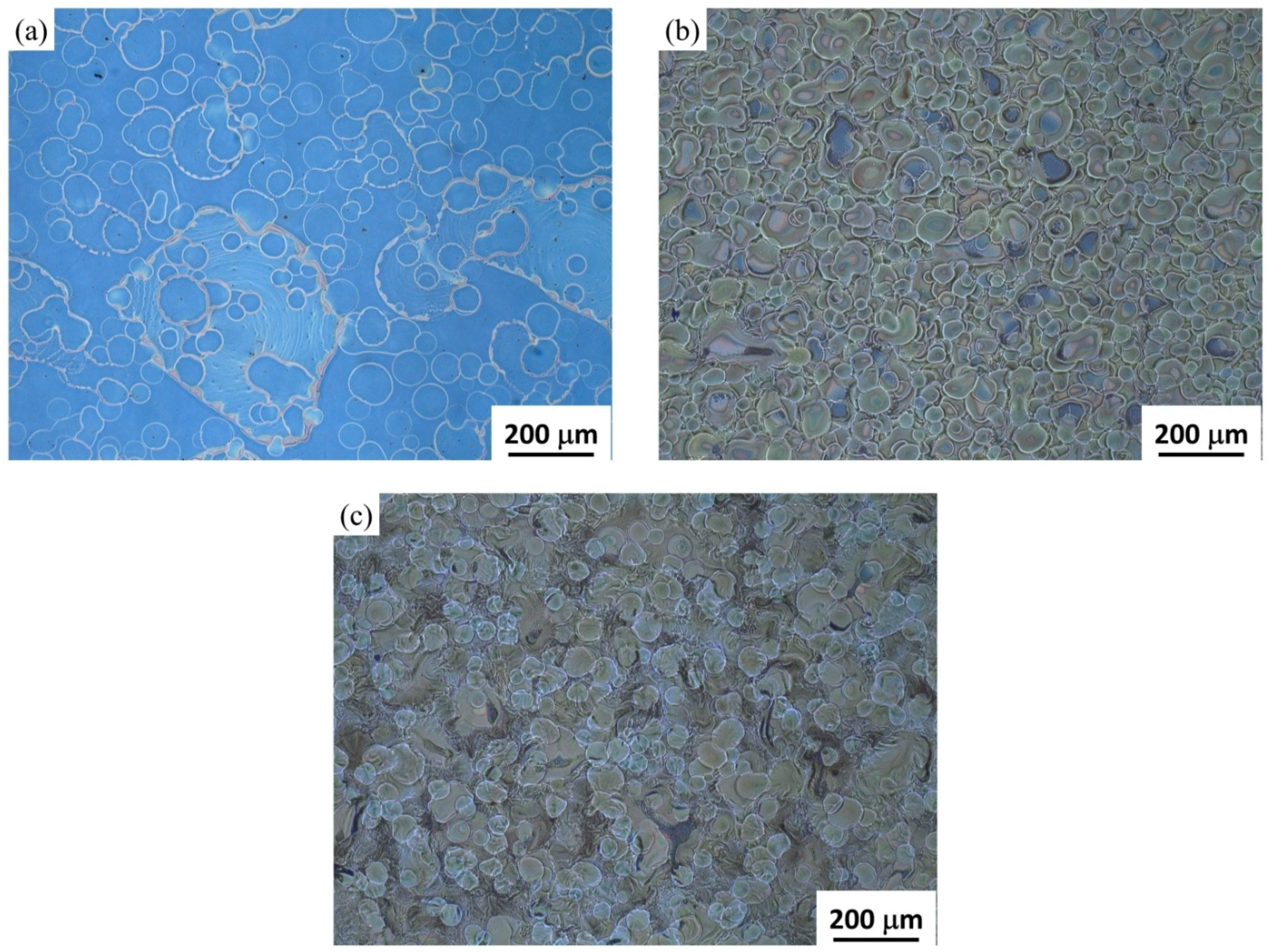
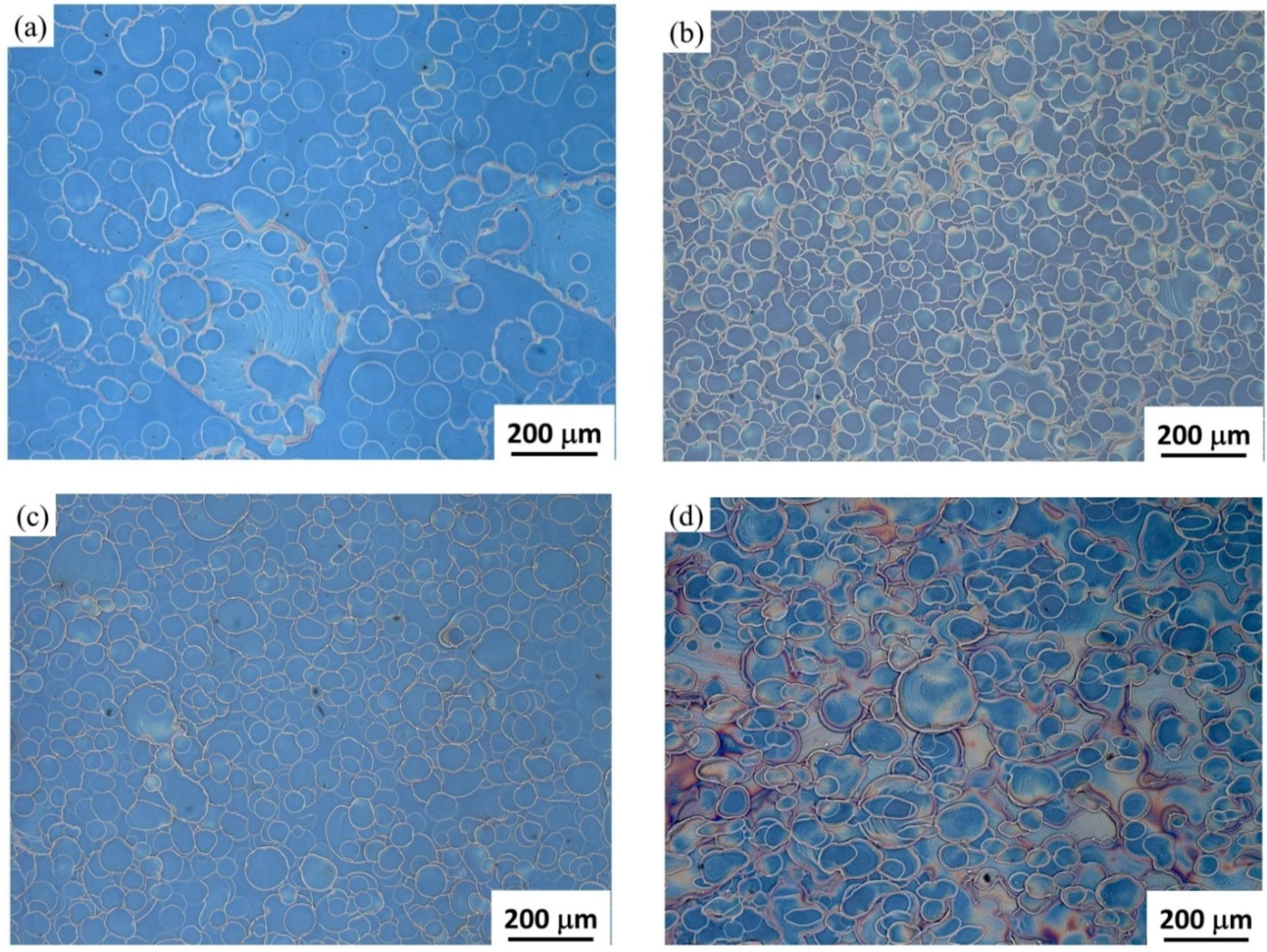
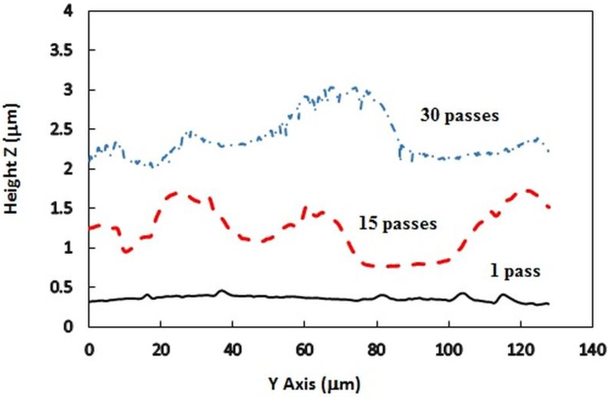
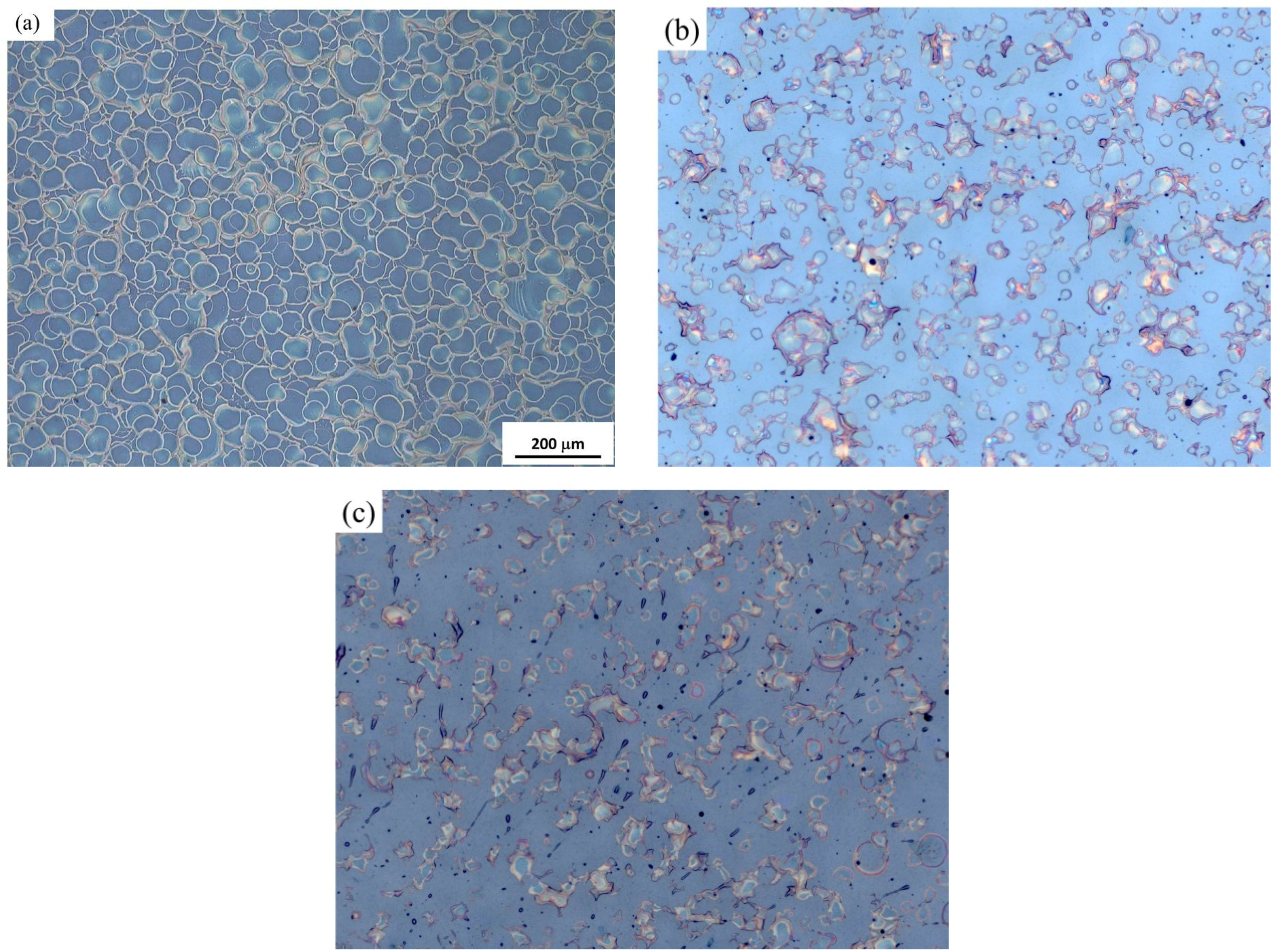
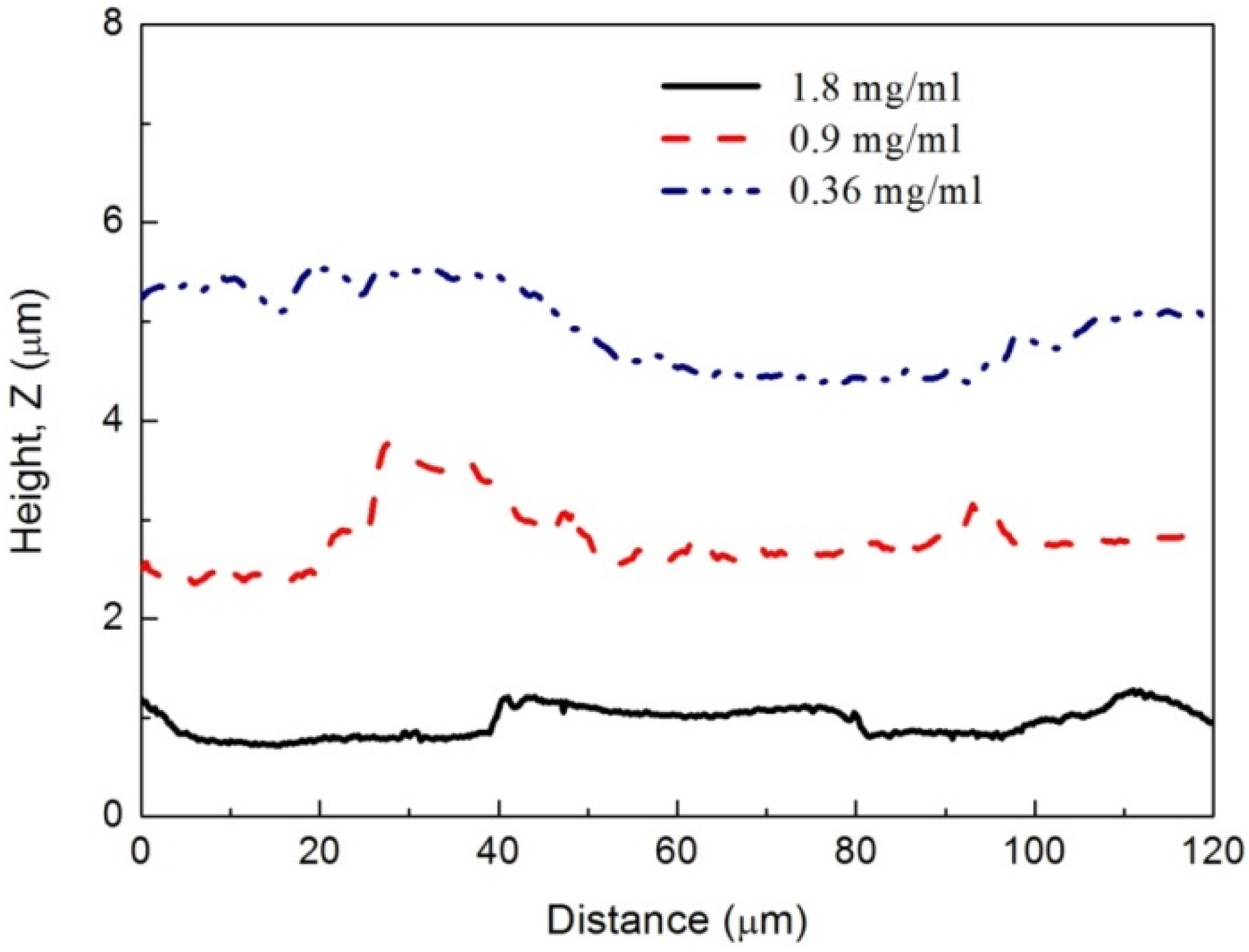
3.2. Surface Topography of Spray-On P3HT:PCBM Films

Figure 4 shows the 3D laser images of spray-on P3HT:PCBM films fabricated on smooth, spun-on PEDOT:PSS films, at 1, 15, and 30 spray passes at a carrier air pressure of 0.1 MPa, a precursor flow rate of 1 mL/min, and a solution concentration of 1.8 mg/mL. The images highlight the surface features and roughness in the z direction. The field of view in the x-y plain is 130 μm × 130 μm. Given that the solution concentration is very low (1.8 mg/mL), one may wonder whether a continuous and intact P3HT:PCBM thin film has formed, particularly when only one deposition layer has been applied. Here, we try to address this question theoretically. In Reference [44], we have derived a mass balance equation for estimating the spray-on thin solid film thickness as follows:
λ s = q x 0 w a u N
where λs is the thin solid film thickness, x0 is a non-dimensional number showing the mass fraction of the solute in the solution (or the density of the solute to the density of the solution), q is the precursor solution flow rate, wa is the diameter of the spray pattern or wetted area on the substrate when the nozzle tip has no motion with respect to the substrate, and uN is the nozzle tip speed. The numerator of Equation (1) is the rate at which the solute is delivered to the substrate, while the denominator is the swept or coated area on the substrate by the spray nozzle. If it is also assumed that each impinging droplet symmetrically spreads, forming a liquid disk or coin, and all disks merge to form a liquid film, the thickness of the liquid film (λl) before evaporation may be obtained as follows:
λ l = q w a u N
In the derivation of Equation (2), it is assumed that the delivered liquid completely covers up and wets the surface. In reality, impinging droplets may not merge, due to limited spreading or the uneven distribution of impinging droplets. If an impinging droplet with diameter D forms a flat disk with diameter d and a height or thickness of λl upon impact, one can express the solution volume flow rate q as a function of other parameters by equating the volume of a droplet with the volume of the liquid disk formed upon impact:
q min = 2 3 w a u N ( D 3 d 2 )
Equation (3) provides an estimate for the minimum required volume flow rate of the sprayed solution (qmin) to cover up the substrate and form a liquid film by the precursor solution. Equation (3) indicates that with an increase in the spreading diameter d, the minimum solution volume flow rate required to form a continuous and connected thin liquid film decreases. The solution concentration should be adjusted accordingly to obtain a thin solid film with a desired thickness (Equation 1). The disk diameter d of the impinged droplet depends on how effectively the droplet can spread on the surface, and depends on droplet dynamics, surface energy, and wettability, as well as on the physical properties of the liquid. Various papers report values between 1.5 and 5 for d/D, e.g., [3,45]. In this work, a conservative value of d = 1.5D was chosen. Under the conditions of our experiments, the minimum flow rate required to form a film is estimated to be about 0.5 mL/min, close to the minimum precursor flow rate used in our experiments for a single pass, viz. 1 mL/min, indicating that a thin film should theoretically form. In the above calculations, the diameter or width of a rectangular wetted area made by the spray on the substrate (wa) was measured to be about 5 cm. Using Equation (2), for a single spray pass, the liquid film thickness will be about 30 μm, which will leave behind a 55 nm P3HT:PCBM thin solid film after complete solvent depletion (Equation 1). When the number of deposition layers increases to 15 and 30, the theory predicts a film with a thickness of 825 and 1650 nm, respectively. These predictions, along with the observations made from the topography of the films shown in Figure 4, indicate that continuous, although rough, P3HT:PCBM films have formed.
Figure 4. Laser topography images of spray-on P3HT:PCBM films: (a) one spray pass, (b) 15 spray passes, and (c) 30 spray passes. Carrier air pressure is 0.1 MPa, precursor flow rate is 1 mL/min, concentration is 1.8 mg/mL, and the field of view is 130 μm × 130 μm. The surface profiles later shown in Figure 7 were found along the red lines shown in this figure.
Coatings 05 00488 g004aCoatings 05 00488 g004b
Figure 5 shows the two-dimensional (2D) optical images of spray-on P3HT:PCBM films made atop the PEDOT:PSS films, using one, 15, and 30 spray passes, while the carrier air pressure is 0.1 MPa, the flow rate is 1 mL/min, and the concentration is 1.8 mg/mL. These images have a large field of view, enabling the observation of the droplet boundaries, the interaction between late impinged droplets with the film, etc. An increase in the number of spray passes results in an increase in the number of splats (dried impinged droplets). In a similar series of images, Figure 6 shows the effect of carrier air pressure on the film morphology for the films deposited using a single spray pass. In images shown in Figure 5 and Figure 6, atop the P3HT:PCBM film, stacked disk-like splats are observed, a phenomenon which is often observed in similar works, e.g., [26,27,28,30,31,32,33,34,35,36,37,38]. Spray droplets impact the substrate by aid of the carrier air, spread on the substrate, and if the precursor flow rate is high enough, the substrate is wettable, and the drying time is long enough, droplets may merge or coalesce, forming a liquid film and a thin solid film after solvent evaporation. Traces of isolated droplets may be observed atop the film (cf. Figure 5 and Figure 6) due to several reasons, such as the coffee-ring effect. If the solvent evaporation characteristic time is longer than the solute diffusion time (for instance, if the substrate temperature is low or if the substrate cools down, because of the impingement of earlier droplets), some isolated droplets may undergo the coffee-ring effect. The coffee-ring effect is due to the precipitation of the solute on the droplet boundaries as a result of rapid solute diffusion toward the edges, and it occurs at low solvent evaporation rates [26,30]. As shown in Figure 5 and Figure 6, coffee rings are observed in all cases, indicating that the substrate kept at 55 °C quickly cools down as a result of droplet impingement so that the forthcoming droplets experience a lower temperature than the initial substrate temperature, and thus undergo coffee-ring formation. Therefore, provided that a high temperature does not deteriorate the film, a substrate temperature higher than 55 °C is recommended to suppress the coffee-ring effect. The quantitative effect of the carrier air pressure on spray characteristics and impinged droplets will be studied later. Also, tuning the precursor flow rate and concentration can affect the surface morphology, which is to be briefly studied later in this paper.
The edges of the splats protrude due to the coffee-ring effect, as can be observed in Figure 4. To investigate this effect, the profile of the red lines drawn on the spray-on P3HT:PCBM films shown in Figure 4 are displayed in Figure 7. As shown in Figure 7, periodic peaks are observed on the profile curves. At the single spray pass, the flat or smooth segment of the profile indicates that those areas of the film are smooth and the film roughness is due to the coffee-ring effect. The periodic nature of the line profile is still observed at 15 and 30 spray passes. The surface roughness of the P3HT:PCBM spray-on films made at various spray passes over a field of view of 130 μm × 130 μm (Figure 4) is shown in Table 2. The roughness is the smallest at one spray pass because a fully intact film has not formed yet. An increase in the number of spray passes results in a significant increase in surface roughness, but a further increase in the number of spray passes up to 30 results in a slight decrease in the surface roughness. The roughness of spray-on films measured over a large field of view (Table 2) is significantly higher than that of the spun-on films over a small field of view (Figure 2). This makes it difficult or impractical to define the thickness value of spray-on P3HT:PCBM films.
Figure 5. 2D optical images of spray-on P3HT:PCBM films, taken by CLSM, showing the surface features; (a) one spray pass, (b) 15 spray passes, and (c) 30 spray passes. Carrier air pressure is 0.1 MPa, flow rate is 1 mL/min, and concentration is 1.8 mg/mL.
Coatings 05 00488 g005
Figure 6. Effect of carrier air pressure on the film topography: 2D optical images of the surface of spray-on P3HT:PCBM films: (a) 0.1 MPa, (b) 0.2 MPa, (c) 0.3 MPa, and (d) 0.4 MPa; a single spray pass was applied in all cases. The flow rate is 1 mL/min, and the concentration is 1.8 mg/mL.
Coatings 05 00488 g006
Figure 7. Effect of the number of spray passes on the film profile: Surface profiles of spray-on P3HT:PCBM films were obtained along an arbitrary line with a length of 130 μm, as shown in Figure 4. Carrier air pressure is 0.2 MPa, flow rate is 1 mL/min, and concentration is 1.8 mg/mL. Note that the y-axis is to show the surface profiles only, and it cannot be used to estimate the film thickness.
Coatings 05 00488 g007
Table 2. Surface RMS roughness at different number of spray deposition passes for a field of view of 130 μm × 130 μm; carrier air pressure is 0.2 MPa, flow rate is 1 mL/min, and concentration is 1.8 mg/mL.
Number of Spray Deposition PassesRMS Roughness (nm)
163
15279
30263
Figure 8 shows the profiles of spray-on P3HT:PCBM films along an arbitrary line (shown in Figure 4), illustrating the effect of changing the solution concentration on the surface profile and roughness. The precursor flow rate is 1 mL/min, and the air carrier pressure is 0.2 MPa. The films were made using 15 spray passes to ensure that a continuous and thick solid film had formed. It can be seen that as the concentration decreases from 1.8 mg/mL to 0.9 mg/mL, and then 0.36 mg/mL, the surface roughness increases. Thus, with other process parameters kept constant, a decrease in solute concentration is not generally beneficial to the surface uniformity. Note that at a lower concentration, to obtain the same effective thickness and light absorbance as that obtained at a higher concentration, additional deposition layers are needed, which may affect the film roughness. Therefore, if low solubility solvents are to be used, other process parameters need to be tuned to make the surface smoother. A practical action to adjust the thickness and at the same time reduce the roughness is to increase the precursor flow rate, as shown in Figure 9.
Figure 8. The effect of precursor concentration on the profile of spray-on P3HT:PCBM films fabricated using 15 deposition passes, with a carrier air pressure of 0.2 MPa, and a flow rate of 1 mL/min. The y-axis is to show the surface profiles only, and it cannot be used to estimate the film thickness.
Coatings 05 00488 g008
Figure 9 shows the optical images of the spray-on P3HT:PCBM films made at various precursor flow rates, using one spray pass, a carrier air pressure of 0.2 MPa, and a precursor solution concentration of 1.8 mg/mL. During droplet impact and, subsequently, the drying process, a droplet may merge with adjacent ones, or the already impinged or forthcoming ones. If the drying time is long enough for droplet coalescence, there will be fewer or even no traces of droplet boundaries, i.e., the coffee rings can be eliminated. The drying time of droplets is proportional to droplet size, the flow rate, and the substrate temperature. In addition, the presence of larger (heavier) droplets leads to larger droplet impact velocities, and thus enhanced spreading, wetting, and coverage. When the flow rate is as small as 1 mL/min, traces of individual droplets are observed, indicating that some of the impinged droplets have dried without complete merging with adjacent droplets. Figure 9 shows that with an increase in the flow rate from 1 to 2 mL/min, and then to 5 mL/min, wetting and film uniformity improve significantly. One can conclude that the flow rate must be kept higher than a critical value to warrant complete wetting and the formation of a uniform film. As an estimate, a precursor flow rate, which is about five times the minimum required flow rate to cover up the substrate, calculated from Equation (3), is recommended. An excessive flow rate is detrimental to the film quality, since the drying process will be delayed. Also, as Equation 3 shows, improving droplet spreading (increasing d/D) via practical options, such as solvent treatment, can improve wetting and film quality.
Figure 9. Effect of precursor flow rate on film morphology: surface topography of spray-on P3HT:PCBM films at (a) 1 mL/min, (b) 2 mL/min, and (c) 5 mL/min. Carrier air pressure is 0.2 MPa, the number of spray passes is one, and the precursor solution concentration is 1.8 mg/mL.
Coatings 05 00488 g009

3.3. Characteristic Parameters of P3HT:PCBM Spray-On Films

The nano-structure of the film is the main parameter that affects the film functionality. Film thickness, surface topography, and roughness also affect the device performance via affecting the contact between thin stacked layers, the fabrication process, and so on. Spun-on films are more uniform and smooth compared to spray-on films. The height difference between the peaks and valleys of spray-on films may be as large as hundreds of nanometers and, therefore, an effective film thickness has to be defined because a geometrical thickness is hard to define. Here, we propose to use an effective thickness for P3HT:PCBM films according to the ability of the film to absorb light, a parameter that can represent the film thickness. Therefore, although the spray-on films have a rough surface, if the film can exhibit satisfactory light absorbance, the high roughness may be tolerated. Absorbance is the common logarithm of the ratio of incident to the transmitted radiant power through a material. Therefore, it shows how much of the incident light is absorbed.
Spray characteristics, such as the spray droplet size, have a significant influence on the film roughness and the film photovoltaic performance [3,26]. However, the subsequent droplet impact dynamics, spreading, and the drying process influence the film characteristics as well. Therefore, we use the size and distribution of the splats on the substrate as a kind of characteristic parameter.

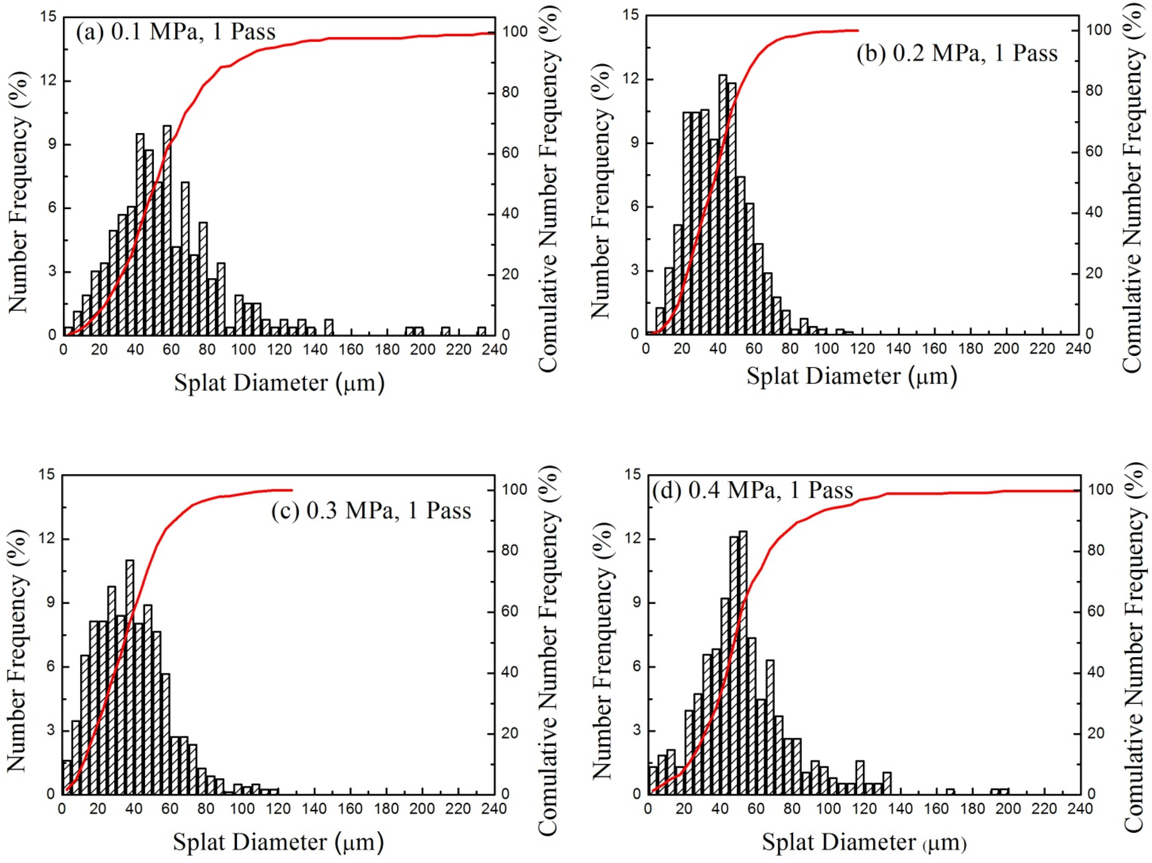
3.3.1. Splat Size Distribution

Here, the splat sizes in each film were obtained using a method similar to finding grain sizes in metallographical samples. The image analysis and boundary detection were carried out by the photo-processing function in the CLSM software. The splat size number frequency and the cumulative distribution were obtained and plotted in Figure 10. The splat size may be estimated by defining the mean diameter Dmean and relative span factor Dspan [26] expressed as follows: Dmean = D0.5 and Dspan = (D0.9D0.1)/D0.5, where D0.1, D0.5, and D0.9 indicate that 10%, 50%, and 90% of the total number of splats have a diameter smaller or equal to these values, respectively. Figure 11 shows the effect of carrier air pressure on the Dmean and Dspan of splats. Several observations are made from Figure 10 and Figure 11. First, the Dmean of splats on the film, for all pressures except for P = 0.3 MPa, is around 50 μm, close to the initial size of the ultrasonically atomized droplets at the nozzle tip, as per the manufacturer’s data sheet. The equilibrium contact angle of our P3HT:PCBM solution droplets at a concentration of 1.8 mg/mL placed on PEDOT:PSS film was measured to be 5.3°, which is quite small and favors sufficient spreading and wetting. However, given that the splat size is comparable to the droplets’ initial size at the nozzle tip, one may conclude that the droplets shrink significantly during the flight and impact or may undergo splashing. Splashing occurs if the impact velocity is sufficiency high [3]. Further investigation is required to fully explain this phenomenon.
With an increase in the carrier air pressure, the mean splat diameter decreases, particularly at P = 0.3 MPa. However, with a further increase in pressure to P = 0.4 MPa, the splat size increases again. The purpose of using the carrier gas in ultrasonic atomization is to carry the droplets and then disperse them to avoid in-flight droplet collision and coalescence. For instance, at zero or low carrier air flow rates, the droplet size increases due to the lack of dispersion, which leads to droplet collision [46]. On the other hand, if the carrier air flow rate or pressure is too high, droplet collision induced by the flow turbulence may result in an increase in the droplet size, a phenomenon which is observed here at P = 0.4 MPa. Therefore, a moderate pressure of 0.2 or 0.3 MPa is beneficial. This effect is also visually observed from the optical images of Figure 6, where an increase in splat size is observed at P = 0.4 MPa.
Figure 10. Splat size distribution at various air pressures: (a) 0.1 MPa, (b) 0.2 MPa, (c) 0.3 MPa, and (4) 0.4 MPa.
Coatings 05 00488 g010
Figure 11. Mean splat diameter Dmean and relative span factor Dspan versus carrier air pressure.
Coatings 05 00488 g011

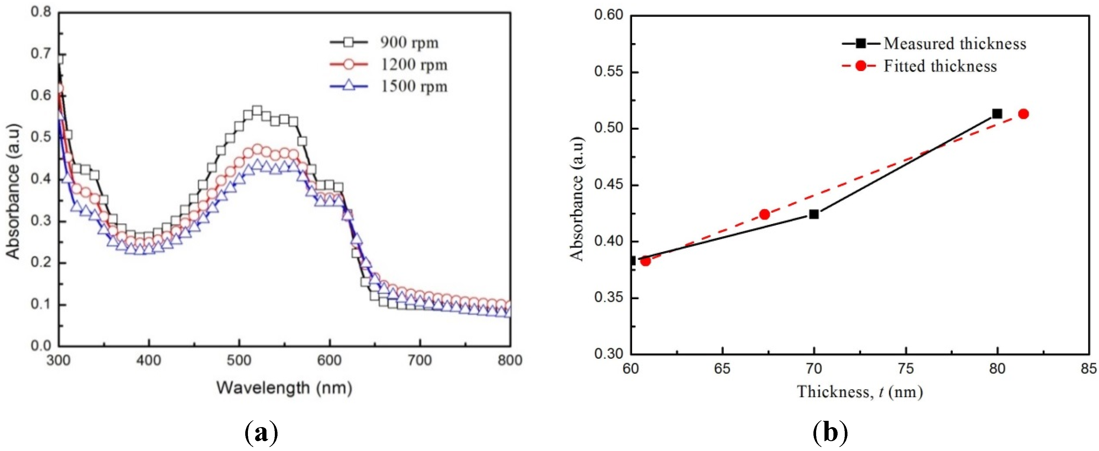
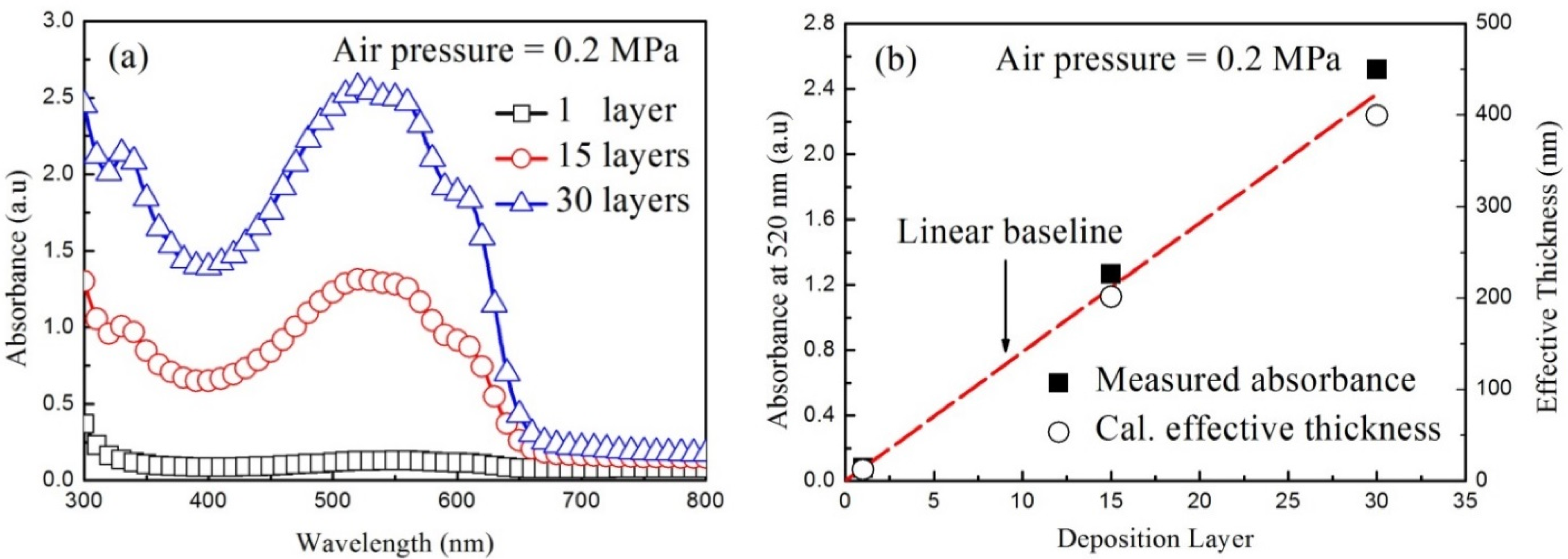
3.3.2. Film Absorbance and Effective Thickness

It was argued before that for rough spray-on films, a geometric thickness is hard to define, but it may be possible to correlate a property of the film, the light absorbance, for P3HT:PCBM film here, with the effective thickness. First we examine the spun-on P3HT:PCBM films, which are fairly smooth, and then extend the results to spray-on films. The absorbance measurement reference line for both spun-on and spray-on films is the surface of the spun-on PEDOT:PSS films underneath the P3HT:PCBM films.
The UV-Visible absorption spectra of the spun-on P3HT:PCBM films produced at various rotation speeds, spanning from the wavelength of 300 nm to 800 nm, are plotted in Figure 12a. The two peaks in Figure 12a occurring around 345 nm and 520 nm are associated with PCBM and P3HT, respectively, and the presence of the shoulder around 600 nm indicates the inter-chain interactions in P3HT [32]. Generally, the red shift happens when the crystallinity of P3HT increases by applying longer drying times through solvent or heat treatment. In our experiments, no heat treatment was applied and the standard solvent, viz. CB, was used; therefore, it is reasonable to observe that the peaks of the films fabricated at different rotation speeds appear at the same wavelengths (cf. Figure 12a). The difference in the film absorbance is due to a change in the film thickness with rotation speed, because absorbance by definition depends on the mass of the film in the direction of the incident light. The plots of the film thickness vs. absorbance for the spun-on P3HT:PCBM films are shown in Figure 12b. The fitting between the thickness and the absorbance by a liner relationship A = at, where A is the value of the absorbance obtained in the experiments and t is the thickness in nm, shows a linear A = 0.0063t with a R2 of 0.98 showing a good fitting. This linear relationship between the geometrical thickness and absorbance in spun-on P3HT:PCBM films will be used to define an effective thickness for the spray-on P3HT:PCBM films by measuring the film absorbance, as discussed below.
Figure 12. (a) UV-Visible absorbance of spun-on P3HT:PCBM films fabricated at different rotation speeds; (b) absorbance of spun-on P3HT:PCBM films versus film thickness, measured by CLSM and also estimated by curve fitting, with R2 = 0.98 (cf. Figure 3). Accordingly, the absorbance (A) and the thickness (t) of spun-on P3HT:PCBM films could be related by A = 0.0063t, where the unit of t is nm. The measurement reference line for absorbance (A) and thickness (t) is the surface of the spun-on PEDOT:PSS film underneath the P3HT:PCBM film.
Coatings 05 00488 g012
Figure 13a shows the UV-Visible absorbance of spray-on P3HT:PCBM films fabricated at various deposition layers or numbers of spray passes at the carrier air pressure of 0.2 MPa. It shows the same peaks as those of spun-on films, indicating that the degrees of crystallinity of the films are identical, regardless of the fabrication method. Having said that, contrary to spin coating in which the film absorbance mostly depends on the thicknesses through the rotation speed, in spray coating all spray characteristics may affect the film uniformity, thickness and, therefore, crystallinity and light absorbance. For instance, longer drying times, through using additional spray passes or higher precursor flow rates or larger impinging droplets, may result in increased crystallinity [26]. This implies that, as shown in Figure 13a, within the range of parameters of this study, the drying time does not need to be long to affect the crystallinity. Figure 13b shows the measured absorbance data points of the spray-on films at the wavelength of 520 nm (peak wavelength) for three deposition layers, as well as an effective film thickness calculated based on the relation between absorbance and thickness obtained for spun-on films, as shown in Figure 12, i.e., A = 0.0063t. It is noted that the spray-on film effective thicknesses defined here and shown in Figure 13b are almost one-quarter of the film thicknesses theoretically estimated by Equation (1). Also, the A = 0.0063t line is plotted in Figure 13b, and it passes through the origin and the data points for absorbance or calculated thickness for a single deposition layer. This line is extended to higher deposition layers to examine whether it will pass through the measured absorbance and calculated effective thickness data points for higher deposition layers. It can be seen that the points representing the values at higher deposition layers are actually very close to this line, indicating that the absorbance (effective thickness) of the spray-on films is linearly proportional to the number of deposition layers. As shown in Figure 7, with an increase in the number of spray passes, the film surface roughness increases. Thus, it can be concluded that the surface roughness has no major influence on the light absorbance of the spray-on P3HT:PCBM films. Film roughness, however, can influence the fabrication of the next layer to be deposited atop the existing layer. For instance, we have found that it is challenging to deposit a continuous nano-thin film on a rough surface using spray or even spin coating. Therefore, it is important to control the film roughness using various strategies, such as the addition of surfactants and co-solvents to the precursor solutions to improve wetting. We have found that the addition of 2-propanol to PEDOT:PSS aqueous solution results in a substantial decrease in the contact angle of PEDOT:PSS droplets on glass, to about 1°, an effect observed by others as well [47]. The contact angle of pristine PEDOT:PSS solution droplets on glass is 21°. Additionally, adjusting other process parameters, such as the precursor flow rate and concentration, as discussed before, is an effective way to control the surface roughness. When it comes to the charge generation and transfer, the film thickness could affect the device performance, although the main factors affecting the device performance are the nano-structure and the charge transfer pathways in the film, as long as the film is thin enough to prevent charge recombination.
Figure 13. (a) UV-Visible absorption spectra of spray-on P3HT:PCBM films, where the measurement reference line is the surface of the spun-on PEDOT:PSS film, underneath the P3HT:PCBM film; (b) the measured absorbance and the calculated effective thickness for three deposition layers (A = 0.0063t, cf. Figure 10) for spray-on P3HT:PCBM films at 520 nm wavelength. In (b), the linear dashed baseline passes through the origin and the absorbance or effective thickness data points for a single deposition layer and extends to a higher number of deposition layers. The line properly predicts the data points for other deposition layers, indicating that a linear relationship exists between the absorbance (effective thickness) and the number of the deposition layers.
Coatings 05 00488 g013

4. Conclusions

The effect of spray parameters on the surface topography, morphology, and light absorbance of spray-on P3HT:PCBM films deposited on spun-on PEDOT:PSS films was studied. A confocal laser scanning microscope (CLSM) was used as the main film characterization tool, and its accuracy was proved sufficient in this work by comparing the roughness results with those obtained by AFM.
The effects of the number of spray passes or deposition layers on the film characteristics and light absorbance were studied. It is found that with an increase in the number of deposition passes, the P3HT:PCBM film integrity and intactness improve, although the surface roughness increases first and then levels off with a further increase in the number of spray passes. The influence of the roughness on the light absorbance of P3HT:PCBM films was examined. It is found that the absorbance has a linear relationship with the number of deposition layers, regardless of the surface roughness.
Due to the high roughness of spray-on P3HT:PCBM films, it is found difficult to define a geometric thickness for such films. However, given that the absorbance has a linear relationship with the film thickness in spun-on smooth films, an effective film thickness was defined and calculated for the spray-on P3HT:PCBM films, which is a linear function of the film absorbance.
The effects of the carrier air pressure employed to carry the ultrasonically generated droplets to the substrate were studied on the film topography. It is found that a low air pressure results in in-flight droplet collision and coalescence due to the lack of droplet dispersion. A high carrier air pressure, on the other hand, results in turbulence and collision and coalescence again. Therefore, a moderate carrier air pressure should be used, which is about 0.2–0.3 MPa, in the range of parameters such as precursor flow rates studied here.
The effects of the precursor flow rate and concentration were also studied on the film topography and roughness. It is found that a precursor flow rate that is about five times that of the minimum flow rate required to entirely cover the surface (Equation (3)) results in better coverage and lower roughness. Low solution concentrations (~1 mg/mL) were used in this study to fabricate spray-on films and to address the need for the elimination of toxic co-solvents currently used to increase the solubility of solar cell materials. However, it is found that in this range, a further decrease in solution concentration leads to an increase in roughness. Therefore, adjustments need to be made between the precursor solution concentration, the flow rate, and the number of spray passes to obtain the desired film thickness with an acceptable roughness.
In this study, the size distribution of P3HT:PCBM splats dried on PEDOT:PSS films were obtained, and it was observed that P3HT:PCBM in CB leave droplet traces on PEDOT:PSS surface. Therefore, to improve the film quality, uniformity, and intactness, several strategies such as using co-solvents and surfactants in the P3HT:PCBM solution, a moderate precursor flow rate, and the application of multiple passes are suggested. A high-enough substrate temperature is also beneficial to suppress the coffee-ring effect.

Acknowledgements

The first author (Y.X) would like to thank the financial support by the China Postdoctoral General Funding, No. 2014M561470. Also, the research funding by Shanghai Municipal Education Commission granted to M.E under the Oriental Scholar program is acknowledged.

Author Contributions

Y. X. and M. E. conceived and designed the experiments; S. G. performed the experiments; Y. X., M. E. and S. G. analyzed the data; Y.X. and S. G. wrote the paper and M. E. revised the paper.

Conflicts of Interest

The authors declare no conflict of interest.

References

  1. Brabec, C.J.; Sariciftci, N.S.; Hummelen, J.C. Plastic solar cells. Adv. Funct. Mater. 2001, 11, 15–26. [Google Scholar] [CrossRef]
  2. You, J.; Dou, L.; Hong, Z.; Li, G.; Yang, Y. Recent trends in polymer tandem solar cells research. Prog. Polym. Sci. 2013, 38, 1909–1928. [Google Scholar] [CrossRef]
  3. Eslamian, M. Spray-on thin film PV solar cells: Advances, potentials and challenges. Coatings 2014, 4, 60–84. [Google Scholar] [CrossRef]
  4. Sariciftci, N.S.; Smilowitz, L.; Heeger, A.J.; Wudl, F. Photoinduced electron transfer from a conducting polymer to Buckminsterfullerene. Science 1992, 258, 1474–1476. [Google Scholar] [CrossRef] [PubMed]
  5. Halls, J.J.M.; Walsh, C.A.; Greenham, N.C.; Marseglia, E.A.; Friend, R.H.; Moratti, S.C.; Holmes, A.B. Efficient photodiodes from interpenetrating polymer networks. Nature 1995, 376, 498–500. [Google Scholar] [CrossRef]
  6. Li, G.; Shrotriya, V.; Yao, Y.; Yang, Y. Investigation of annealing effects and film thickness dependence of polymer solar cells based on poly(3-hexylthiophene). J. Appl. Phys. 2005, 98. [Google Scholar] [CrossRef]
  7. Zeng, L.; Tang, C.W.; Chen, S.H. Effects of active layer thickness and thermal annealing on polythiophene: Fullerene bulk heterojunction photovoltaic devices. Appl. Phys. Lett. 2010, 97. [Google Scholar] [CrossRef]
  8. Flack, W.W.; Soong, D.S.; Bell, A.T.; Hess, D.W. A mathematical model for spin coating of polymer resists. J. Appl. Phys. 1984, 56, 1199–1206. [Google Scholar] [CrossRef]
  9. Bornside, D.E.; Macosko, C.W.; Scriven, L.E. Spin coating: One-dimensional model. J. Appl. Phys. 1989, 66, 5185–5193. [Google Scholar] [CrossRef]
  10. Hall, D.B.; Underhill, P.; Torkelson, J.M. Spin coating of thin and ultrathin polymer films. Polym. Eng. Sci. 1998, 38, 2039–2045. [Google Scholar] [CrossRef]
  11. Cheung, K.P.; Grover, R.; Wang, Y.; Gurkovich, C.; Wang, G.; Scheinbeim, J. Substrate effect on the thickness of spin-coated ultrathin polymer film. Appl. Phys. Lett. 2005, 87. [Google Scholar] [CrossRef]
  12. Extrand, C.W. Spin coating of very thin polymer films. Polym. Eng. Sci. 1994, 34, 390–394. [Google Scholar] [CrossRef]
  13. Kim, Y.; Choulis, S.A.; Nelson, J.; Bradley, D.D.C.; Cook, S.; Durrant, J.R. Device annealing effect in organic solar cells with blends of regioregular poly(3-hexylthiophene) and soluble fullerene. Appl. Phys. Lett. 2005, 86. [Google Scholar] [CrossRef]
  14. Yang, X.; Loos, J.; Veenstra, S.C.; Verhees, W.J.H.; Wienk, M.M.; Kroon, J.M.; Michels, M.A.J.; Janssen, R.A.J. Nanoscale morphology of high-performance polymer solar cells. Nano Lett. 2005, 5, 579–583. [Google Scholar] [CrossRef] [PubMed]
  15. Reyes-Reyes, M.; Kim, K.; Carroll, D.L. High-efficiency photovoltaic devices based on annealed poly(3-hexylthiophene) and 1-(3-methoxycarbonyl)-propyl-1-phenyl-(6,6)C61 blends. Appl. Phys. Lett. 2005, 87. [Google Scholar] [CrossRef]
  16. Liu, Y.X.; Lü, L.F.; Ning, Y.; Lu, Y.Z.; Lu, Q.P.; Zhang, C.M.; Fang, Y.; Tang, A.W.; Hu, Y.F.; Lou, Z.D.; et al. Effects of acetone-soaking treatment on the performance of polymer solar cells based on P3HT/PCBM bulk heterojunction. Chin. Phys. B 2014, 23. [Google Scholar] [CrossRef]
  17. Li, G.; Shrotriya, V.; Huang, J.; Yao, Y.; Moriarty, T.; Emery, K.; Yang, Y. High-efficiency solution processable polymer photovoltaic cells by self-organization of polymer blends. Nat Mater. 2005, 4, 864–868. [Google Scholar] [CrossRef]
  18. Kim, K.; Liu, J.; Namoothiry, M.A.G.; Carroll, D.L. Roles of donor and acceptor nanodomains in 6% efficient thermally annealed polymer photovoltaics. Appl. Phys. Lett. 2007, 90. [Google Scholar] [CrossRef]
  19. Riede, M.K.; Mueller, T.; Maennig, B.; Leo, K.; Sylvester-Hvid, K.O.; Zimmermann, B.; Niggemann, M.; Gombert, A. Comment on “roles of donor and acceptor nanodomains in 6% efficient thermally annealed polymer photovoltaics”. Appl. Phys. Lett. 2008, 92. [Google Scholar] [CrossRef]
  20. Shaheen, S.E.; Radspinner, R.; Peyghambarian, N.; Jabbour, G.E. Fabrication of bulk heterojunction plastic solar cells by screen printing. Appl. Phys. Lett. 2001, 79, 2996–2998. [Google Scholar] [CrossRef]
  21. Hoth, C.N.; Choulis, S.A.; Schilinsky, P.; Brabec, C.J. High photovoltaic performance of inkjet printed polymer: Fullerene blends. Adv. Mater. 2007, 19, 3973–3978. [Google Scholar] [CrossRef]
  22. Hong, S.; Yi, M.; Kang, H.; Kong, J.; Lee, W.; Kim, J.-R.; Lee, K. Effect of solvent on large-area polymer-fullerene solar cells fabricated by a slot-die coating method. Sol. Energy Mater. Sol. Cells 2014, 126, 107–112. [Google Scholar] [CrossRef]
  23. Zabihi, F.; Xie, Y.; Gao, S.; Eslamian, M. Morphology, conductivity, and wetting characteristics of PEDOT:PSS thin films deposited by spin and spray coating. Appl. Surf. Sci. 2015, 338, 163–177. [Google Scholar] [CrossRef]
  24. Notte, L.L.; Mineo, M.; Polino, G.; Susanna, G.; Brunetti, F.; Brown, M.T.; Carlo, D.A.; Reale, A. Fabrication of fully-spray-processed organic photovoltaic modules by using an automated process in air. Energy Technol. 2013, 1, 757–762. [Google Scholar] [CrossRef]
  25. Tait, G.J.; Wong, C.; Cheyns, D.; Turbiez, M.; Rand, P.B.; Heremans, P. Ultrasonic spray coating of 6.5% efficient diketopyrrolopyrrole-based organic photovoltaics. IEEE J. Photovolt. 2014, 4, 1538–1544. [Google Scholar] [CrossRef]
  26. Byung-Kwan, Y.; Doojin, V.; Jang, J.; Na, S.-I.; Kim, S.-S.; Mi-Kyoung, K.; Kim, D.-Y. Factors to be considered in bulk heterojunction polymer solar cells fabricated by the spray process. IEEE J. Sel. Topics Quantum Electron. 2010, 16, 1838–1846. [Google Scholar]
  27. Girotto, C.; Rand, B.P.; Genoe, J.; Heremans, P. Exploring spray coating as a deposition technique for the fabrication of solution-processed solar cells. Sol. Energy Mater. Sol. Cells 2009, 93, 454–458. [Google Scholar] [CrossRef]
  28. Hoth, C.N.; Steim, R.; Schilinsky, P.; Choulis, S.A.; Tedde, S.F.; Hayden, O.; Brabec, C.J. Topographical and morphological aspects of spray coated organic photovoltaics. Org. Electron. 2009, 10, 587–593. [Google Scholar] [CrossRef]
  29. Tait, J.G.; Rand, B.P.; Heremans, P. Concurrently pumped ultrasonic spray coating for donor:acceptor and thickness optimization of organic solar cells. Org. Electron. 2013, 14, 1002–1008. [Google Scholar] [CrossRef]
  30. Majumder, M.; Rendall, C.; Li, M.; Behabtu, N.; Eukel, J.A.; Hauge, R.H.; Schmidt, H.K.; Pasquali, M. Insights into the physics of spray coating of SWNT films. Chem. Eng. Sci. 2010, 65, 2000–2008. [Google Scholar] [CrossRef]
  31. Lee, J.-h.; Sagawa, T.; Yoshikawa, S. Morphological and topographical characterizations in spray coated organic solar cells using an additional solvent spray deposition. Org. Electron. 2011, 12, 2165–2173. [Google Scholar] [CrossRef]
  32. Steirer, K.X.; Reese, M.O.; Rupert, B.L.; Kopidakis, N.; Olson, D.C.; Collins, R.T.; Ginley, D.S. Ultrasonic spray deposition for production of organic solar cells. Sol. Energy Mater. Sol. Cells 2009, 93, 447–453. [Google Scholar] [CrossRef]
  33. Chen, L.-M.; Hong, Z.; Kwan, W.L.; Lu, C.-H.; Lai, Y.-F.; Lei, B.; Liu, C.-P.; Yang, Y. Multi-source/component spray coating for polymer solar cells. ACS Nano 2010, 4, 4744–4752. [Google Scholar] [CrossRef] [PubMed]
  34. Vak, D.; Kim, S.-S.; Jo, J.; Oh, S.-H.; Na, S.-I.; Kim, J.; Kim, D.-Y. Fabrication of organic bulk heterojunction solar cells by a spray deposition method for low-cost power generation. Appl. Phys. Lett. 2007, 91. [Google Scholar] [CrossRef]
  35. Abdellah, A.; Virdi, K.S.; Meier, R.; Döblinger, M.; Müller-Buschbaum, P.; Scheu, C.; Lugli, P.; Scarpa, G. Successive spray deposition of P3HT/PCBM organic photoactive layers: Material composition and device characteristics. Adv. Funct. Mater. 2012, 22, 4078–4086. [Google Scholar] [CrossRef]
  36. Lee, J.-h.; Sagawa, T.; Yoshikawa, S. Thickness dependence of photovoltaic performance of additional spray coated solar cells. Thin Solid Films 2013, 529, 464–469. [Google Scholar] [CrossRef]
  37. Girotto, C.; Moia, D.; Rand, B.P.; Heremans, P. High-performance organic solar cells with spray-coated hole-transport and active layers. Adv. Funct. Mater. 2011, 21, 64–72. [Google Scholar] [CrossRef]
  38. Ishikawa, T.; Nakamura, M.; Fujita, K.; Tsutsui, T. Preparation of organic bulk heterojunction photovoltaic cells by evaporative spray deposition from ultradilute solution. Appl. Phys. Lett. 2004, 84, 2424–2426. [Google Scholar] [CrossRef]
  39. Zabihi, F.; Eslamian, M. Substrate vibration-assisted spray coating (SVASC): Significant improvement in nano-structure, uniformity, and conductivity of PEDOT: PSS thin films for organic solar cells. J. Coat. Technol. Res. 2015, 12, 711–719. [Google Scholar] [CrossRef]
  40. Eslamian, M. A Mathematical model for the design and fabrication of polymer solar cells by spray coating. Drying Technol. 2013, 31, 405–413. [Google Scholar] [CrossRef]
  41. Minsky, M. Memoir on inventing the confocal scanning microscope. Scanning 1988, 10, 128–138. [Google Scholar] [CrossRef]
  42. Davidovits, P.; Egger, M.D. Scanning laser microscope. Nature 1969, 223, 831–831. [Google Scholar] [CrossRef] [PubMed]
  43. Davidovits, P.; Egger, M.D. Scanning laser microscope for biological investigations. Appl. Opt. 1971, 10, 1615–1619. [Google Scholar] [CrossRef] [PubMed]
  44. Eslamian, M.; Newton, J.E. Spray-on PEDOT:PSS and P3HT:PCBM thin films for polymer solar cells. Coatings 2014, 4, 85–97. [Google Scholar] [CrossRef]
  45. Yarin, A.L. Droplet impact dynamics: Splashing, spreading, receding, bouncing... Annu. Rev. Fluid Mech. 2006, 38, 159–192. [Google Scholar] [CrossRef]
  46. Eslamian, M.; Ashgriz, N. Effect of precursor, ambient pressure, and temperature on the morphology, crystallinity, and decomposition of powders prepared by spray pyrolysis and drying. Powder Technol. 2006, 167, 149–159. [Google Scholar] [CrossRef]
  47. Girotto, C.; Moia, D.; Rand, B.P.; Aernouts, T.; Heremans, P. Efficient polymer solar cells via an all-spray-coated deposition. In Proceedings of 35th IEEE Photovoltaic Specialists Conference, Honolulu, HI, USA, 20–25 June 2010; pp. 001068–001072.

