Review

Metal-Polymer Nanocomposites: (Co-)Evaporation/(Co)Sputtering Approaches and Electrical Properties

by
Vanna Torrisi
1,* and
Francesco Ruffino
2,3,*
1
Laboratory for Molecular Surface and Nanotechnology (LAMSUN), Department of Chemical Sciences, University of Catania, Viale A. Doria 6, 95125 Catania, Italy
2
Dipartimento di Fisica ed Astronomia-Università di Catania, via S. Sofia 64, 95123 Catania, Italy
3
MATIS IMM-CNR, via S. Sofia 64, 95123 Catania, Italy
*
Authors to whom correspondence should be addressed.
Coatings 2015, 5(3), 378-424; https://doi.org/10.3390/coatings5030378
Submission received: 5 June 2015 / Revised: 29 June 2015 / Accepted: 22 July 2015 / Published: 29 July 2015
(This article belongs to the Special Issue Multifunctional Organic-Inorganic Hybrid Thin Films and Coatings)

Abstract

:
In this review, we discuss the basic concepts related to (co-)evaporation and (co)sputtering based fabrication methods and the electrical properties of polymer-metal nanocomposite films. Within the organic-inorganic hybrid nanocomposites research framework, the field related to metal-polymer nanocomposites is attracting much interest. In fact, it is opening pathways for engineering flexible composites that exhibit advantageous electrical, optical, or mechanical properties. The metal-polymer nanocomposites research field is, now, a wide, complex, and important part of the nanotechnology revolution. So, with this review we aim, starting from the discussion of specific cases, to focus our attention on the basic microscopic mechanisms and processes and the general concepts suitable for the interpretation of material properties and structure–property correlations. The review aims, in addition, to provide a comprehensive schematization of the main technological applications currently in development worldwide.

1. Introduction

Organic-inorganic hybrid nanomaterials have innovative characteristics which arise from the synergism between the properties of the components. Such a behavior allows their application in many fields such as electronics, optoelectronics, biomedicine, energy, etc. [1,2,3,4,5]. Organic-inorganic hybrid nanomaterials cross the flexibility, transparence, and easy of processability of soft matter (organic materials) with the thermal stability, mechanical, optical and electric properties of hard matter (inorganic materials). Surely, the development of simple, versatile low-cost methodologies for the design, production and atomic-scale manipulation of innovative functional organic-inorganic hybrid nanomaterials is the key step towards their mass-production and real technological applications. Also, the complete experimental and theoretical characterizations of their physical and chemical properties (electronic, optical, mechanical, etc.) is fundamental to this end. Crucial is, finally, the integration of such materials in real devices for applications of significant social impact.
Within the organic-inorganic hybrid nanomaterials research framework, in particular, the field related to metal-polymer nanocomposites is attracting much interest [6,7,8,9]. The mixing of polymers and nanoparticles (NPs) is creating new directions for engineering versatile composites characterized by peculiar electrical, optical, or mechanical properties. Among the most important materials for nanotechnology, metal NPs are particularly interesting, due to the very unusual properties that they exhibit. Metals undergo considerable property changes by size reduction, and their composites with polymers are very interesting for functional applications. The new properties observed in nanoscale metals arise from quantum-size effects (i.e., electron confinement and surface effect). These properties are size-dependent and can be tuned by changing the metal size and shape. Confinement effects arise in nanoscale metal domains since conduction electrons are allowed to move within a very small space, which is comparable to their De Broglie wavelength; consequently, their states are quantized just like in the atoms. These properties are routinely exploited in plasmonic, sensing, electrical, catalytic applications [6,7,8,9]. Several of these distinctive chemical-physics characteristics of metal NPs can be used to provide special functionalities to polymers by their mixing. From a technological point of view, polymers have a variety of useful characteristics: they can be an electrical and thermal insulator or conductor, may have a hydrophobic or hydrophilic nature, can be mechanically hard, plastic, or rubbery, and so on. In addition, generally, polymers are low-cost materials, versatile, and can be processed into thin films.
The controlled design and fabrication of metal-polymer nanocomposites lead to artificial functional materials taking advantages from the properties of both the components. For example, in recent years, nanostructured materials fabricated by metal NPs and thin metal nano-grained films deposited on or embedded in soft polymeric substrates have emerged in the developing field of organic electronics [10,11,12]. Several prototypes of organic transistors [10], light-emitting diodes [11], and solar cells [12] have been proposed. Regarding the exploitation of the particular metal/polymer system, the key point of study is the interaction occurring at the metal-polymer interface. In fact, properties as film adhesion and electrical contact properties are determined by the interface structure [6,7,8,9,13]. So, of key importance is understanding the growth kinetics of the metal film on/in the polymer surface/matrix, how the polymer influences the metal film morphology, and the electron transport mechanism in the nanocomposite.
On the basis of the previous considerations, in this paper, we review basic aspects of (co-)evaporation and (co-)sputtering based synthesis methods of metal-polymer nanocomposites and some electrical properties of such systems. In particular, the review is organized as follows:
The first part (Section 2) is devoted to (co-)evaporation and (co-)sputtering based fabrication methods for metal-polymer nanocomposites. This part reviews the basic kinetics concepts related to the phenomena occurring during metal depositions, from vapor phase processes (metals evaporation or sputtering), on polymeric surfaces leading to the formation of metal NPs or films on such surfaces (Section 2.1); the basic phenomena involved in the co-deposition process of polymers and metals leading to the formation of polymeric films with embedded metal NPs, and the corresponding structural-physical parameters correlation (Section 2.2); the basic kinetics concepts related to the embedding phenomenon of metal NPs deposited on polymeric layers when annealing processes above the polymer glass-transition temperature are performed as an alternative fabrication method to the co-deposition route (Section 2.3). In Section 2, the attention is focused on physical vapor deposition techniques (evaporation, sputtering) since they are promising methods for the preparation of nanocomposite films in a dry process (unlike wet chemical synthesis, physical vapor deposition methods are residual and solvent free processes). Additionally, technological advantages of the physical vapor deposition techniques over other techniques create the possibility to realize a higher deposition rate (as demonstrated by RF magnetron deposition of different polymers), an excellent conformity over complex topography and the possibility of a good composite film uniformity on relatively large substrates. Naturally, several interesting and promising fabrication techniques have been developed for the production of metal-polymer nanocomposites in addition to those based on (co-)evaporation and (co-)sputtering approaches [7,14,15,16], as, for example, those based on UV-curing [17], direct chemical reduction [18], in-situ and ex-situ polymerization [19], and ion implantation [20]. In this review, we choose to focus our attention on the (co-)evaporation and (co-)sputtering approaches since they are, surely, those that will meet large-scale production requirements in order to achieve real industrial scalability in the near future.
The second part (Section 3) is devoted to the electrical properties of metal-polymer nanocomposites. These properties are worth consideration because the addition of metallic nanostructures to insulating or conducting polymers allows to finely tune the electrical properties of the resulting films in a way that is particular to nanocomposite films.
In particular, this section deals with the electrical properties of the nanocomposite films composed by: (1) metal NPs deposited on polymeric films, (2) metal NPs co-deposited with polymer film and of (3) metal NPs embedded in polymeric film. Finally, particular attention is devoted to conducting polymer based nanocomposites films and their technological applications.

2. (Co-)Evaporation and (Co-)Sputtering Fabrication Methods for Metal-Polymer Nanocomposites

2.1. Thin Metal Film Fabrication on Polymeric Surfaces by Vapor Phase Depositions: Basic Kinetics

When using vapor phase deposition techniques (such as evaporation or sputtering) to growth metal NPs or films on polymeric surfaces, noble metals like Au and Ag grow, during the initial stage, as spherical clusters on polymer surfaces [13,21,22,23,24,25,26,27,28,29,30,31,32], i.e., according to a Volmer-Weber [33] growth mode. This is due to a higher (two orders of magnitude) cohesive energy of metals with respect to the polymers’ cohesive energy. Moreover, the interaction between noble metals and polymers is very weak compared to the metal-metal binding forces [5,6,7,8,30,31,32]. So, noble metals do not wet, in general, polymer surfaces. They form clusters in the initial stage of deposition so that a distribution of small islands with circular cross section is obtained on the polymeric surface (i.e., three-dimensional spherical-like shapes) and their sizes are represented by the diameter D. For example, Figure 1 shows atomic force microscopy (AFM) images of: (a) 25 nm-thick Au layer evaporated (at room-temperature) onto 11 nm-thick poly(N-vinylcarbazole) (PVK) spin-coated film on glass [13], (b) and (c) 2 nm-thick Au layer sputtered (at room-temperature) onto 200 nm-thick polystyrene (PS) and poly(methyl methacrylate) (PMMA), respectively, spin-coated on Si [21].
Figure 1. AFM images of: (a) 25 nm-thick Au layer evaporated (at room-temperature) onto 11 nm-thick poly(N-vinylcarbazole) spin-coated film on glass; (b,c) 2 nm-thick Au layer sputtered (at room temperature) onto 200 nm-thick polystyrene and poly(methyl methacrylate), respectively, spin-coated on Si. ((a): reproduced with permission from [13], Copyright American Chemical Society 2009; (b,c) reproduced with permission from [21], Copyright Springer 2011).
Coatings 05 00378 g001
The almost-circular cross-section of the Au nanostructures on the polymeric surfaces is recognizable. This initial growth stage is known as a “low-coverage” growth stage [21,34]. Increasing the amount of deposited metal (i.e., the thickness h of the grown metal film), the film is in a “medium-coverage” growth stage [21,34]: in this step, the metal islands grow in size, partially coalesce, and form worm-like structures. For example, Figure 2 shows: in (a) and (b) AFM images of 10 nm-thick Au layer sputtered (at room temperature) onto 200 nm-thick PS and PMMA, respectively, spin-coated on Si [21]; in (c) and (d) scanning electron microscopy (SEM) analyses of 4 nm-thick Au evaporated (at room-temperature) onto polyimide (pyromellitic dianhydride-oxydianiline, PMDA-ODA) and poly(ethylene terephthalate) (PET), respectively [26]. At higher h, a “high-coverage” growth stage occurs for the metal film [21,34]: island percolation (islands grow longer and are connected originating a continuous network across the surface) is obtained and, finally, the rough and continuous metal film is formed by a holes filling process. As an example, Figure 3 shows AFM images of 20 nm-thick Au layer sputtered (at room temperature) onto 200 nm-thick PS (a) and PMMA (b) [21].
Figure 2. (a,b) AFM images of 10 nm-thick Au layer sputtered (at roomtemperature) onto 200 nm-thick polystyrene and poly(methyl methacrylate), respectively, spin-coated on Si. In (c,d) SEM images (200 nm by 120 nm) of 4 nm-thick Au evaporated (at room temperature) onto polyimide and poly(ethylene terephthalate), respectively. ((a,b): reproduced with permission from [21], Copyright Springer 2011; (c,d): reproduced with permission from [26], Copyright Elsevier 1997).
Coatings 05 00378 g002
Figure 3. (a,b) AFM images of 20 nm-thick Au layer sputtered (at room temperature) onto 200 nm-thick polystyrene and poly(methyl methacrylate), respectively, spin-coated on Si. (Reproduced with permission from [21], Copyright Springer 2011).
Coatings 05 00378 g003
The critical metal film thicknesses separating the growth stages are dependent on the specific metal and polymer characteristics (such as surface free energies) and on their specific interaction (such as adhesion energy). Generally, the metal morphology evolution on a non-wetting substrate can be studied by the interrupted coalescence model (ICM) [21,34,35,36,37], the kinetic freezing model (KFM) [28,29,30,31,32,33,34,35,36,37,38,39,40], and the Vincent model [40,41]. Following the ICM model, at the initial stages of growth metal NPs grow on the surface due to homogeneous and heterogeneous nucleation [30,31,32,33]. So, for atoms deposited on the substrate from the vapor phase, a series of kinetic processes occurs: thermal accommodation on the substrate, surface diffusion of the atoms on the surface, small clusters formation to initiate nucleation, then island formation and growth. Increasing the amount of deposited atoms, islands grow, contact each other, and coalesce (i.e., two or more islands merge) into larger, but still compact, islands. During this coalescence process, a wiping phenomenon can take place: during the formation of a larger island by the coalescence process of two smaller islands, part of the substrate which was previously covered is wiped clean. As a consequence, larger islands on the substrate are formed but they are separated by gaps between them. So, at the later growth stage, a partial coalescence occurs (instead of a full coalescence) leading to the formation of elongated structures with worm-like shape. The cross-over from full coalescence (compact islands) is identified by the islands critical radius Rc that depends on materials and temperature. The KFM model, in addition, defines quantitatively Rc by the condition that the time for two islands to coalesce equals the time for the islands to touch their neighbors. Such a condition leads to [38].
R c 4 = D s t c γ m Ω 4 / 3 k T
where Ds is the surface diffusion coefficient of the metal atoms on the substrate, tc the critical time at which the size of the islands equals Rc, γm the metal surface free energy, Ω the metal atomic volume, k the Boltzmann constant, and T the absolute temperature. Increasing, further, the amount of deposited atoms, the worm-like islands grow longer and thicker, and finally percolation occurs. Then, a continuous, but rough, film is formed by a hole-filling process.
After the very first particles’ nucleation stage, i.e., when the low and medium coverage stages occur, increasing the metal film thickness h (or the deposition time t, if all other parameters are fixed, so that h   t) the diameter D of the particles increases, the particles surface density N (particles/cm2) decreases (due to the particles coalescence process) and the surface coverage P (area covered by the particles/total surface area) increases. As examples, Figure 4a reports the average area, surface density and surface coverage evolution (as a function of the film thickness h) for Au particles formed on PS surface by room-temperature Au evaporation, accordingly to Smithson et al. [26]. The data are limited to the 0.1–4 nm range. In addition, Figure 4b reports density and radius versus effective thickness for NPs obtained by Au evaporation (at room temperature) onto polyimide, according to Faupel et al. [30]. In this last case, it is interesting, in particular, to note the behavior of the NPs’ density: in fact, two regimes can be easily recognized in this plot. The first one is the very first Au NPs’ nucleation stage on the polyimide surface. It occurs at Au effective thicknesses below 0.2 nm. In this stage, the NPs surface density increases by increasing the Au thickness. After this nucleation stage, the NPs’ growth stage occurs (at thicknesses above 0.2 nm) and, correspondently, the NPs’ surface density decreases as the film thickness increases. Some of these data correspond to the transmission electron microscopy images in Figure 4c–f. These images show examples for the different stages of Au growth onto polyimide at a rate of 0.1 nm/min at room temperature: 0.1 nm (a), 0.2 nm (b), 0.6 nm (c), and 2.4 nm (d) [31].
Figure 4. (a) Average area, surface density and surface coverage evolution (as a function of the film thickness h) for Au particles formed on polystyrene surface by room temperature Au evaporation. (b) Density and radius versus effective thickness, for NPs obtained by Au evaporation (at room temperature) onto polyimide. (cf) TEM images corresponding to Au deposited at different thicknesses onto polyimide at a rate of 0.1 nm/min at room temperature: 0.1 nm (c), 0.2 nm (d), 0.6 nm (e), and 2.4 nm (f). ((a): reproduced with permission from [26], Copyright Elsevier 1997; (b): reproduced with permission from [30], Copyright AIP Publishing LLC 1999; (c–f): reproduced with permission from [31], Copyright Taylor & Francis 2000).
Coatings 05 00378 g004
By the comparison of Figure 4a,b, in particular, it is interesting to note that where in (a) the Au cluster density on the PS surface decreases in the 0.1–4 nm thickness range, while in (b) the Au cluster density on the polyimide surface increases for thicknesses <0.2 nm and, then, decreases for thicknesses ≥0.2 nm. This is a clear evidence of the effect of the substrate nature on the nucleation process of the deposited metal. Evidently, the Au atoms surface diffusion coefficient is (at room temperature) higher on the PS surface than on the polyimide surface (probably related to a higher adhesion energy of Au atoms on the polyimide surface than on the PS surface): so, the Au clusters nucleation stage is completed at lower thicknesses on the PS surface with respect to the polyimide surface.
To apply the ICM model, we can consider the data reported in Figure 5: in this case, the average Au particles sizes <R> (width, i.e., radius) and <D> (length, i.e., diameter), formed by room temperature sputtering depositions of Au on PS and PMMA surfaces, respectively, are reported as a function of the deposition time t (at a rate of about 0.06 nm/s) [21]. In the analyzed 30–180 s range, from such data, the effect of the particles’ partial coalescence process can be observed: at t ≤ 90 s the plot in Figure 5 indicates <R> ≈ <D> so that, in this stage, Au NPs with circular cross section are formed. As expected, in this stage, the Au atoms form 3D islands with droplet-like shapes and their sizes are represented by their diameters D (both on PS and PMMA) according to a Volmer–Weber growth mode. At t > 90 s, the islands lose the spherical shape: they become elongated and their sizes are described by their average longest and shortest dimensions. As a consequence, at t > 90 s, the Au islands surface density N decreases (Figure 6a) and the fraction P of substrate coated by Au increases (Figure 6b). Overall, increasing t, the Au island morphology evolves from droplet-like islands to worm-like structures (Figure 1 and Figure 2). To highlight the generality of such considerations, we point out, for example, that for the evolution of P versus h, similar results were found by Kaune et al. [13] concerning Au sputtered on poly(N-vinylcarbazole) (Figure 6c).
The plot in Figure 5 shows also that the Au islands start to grow longer in one dimension at t > tc where tc indicates a critical deposition time: tc ≈ 110.2 s and tc ≈ 108.1 s for the Au NPs on the PS and on the PMMA surfaces, respectively. Recalling the ICM model, the mean island radius at which partial coalescence occurs, i.e., the critical radius <Rc>, can be evaluated by crossing the two lines in Figure 5: <Rc> ≈ 8.7 nm and <Rc> ≈ 7.6 nm for the Au NPs on the PS and on the PMMA surfaces, respectively. Now, following the KFM model, Equation (1), using T = 300 K, γ = 83 × 10−3 J/m2 [21] and Ω = 1.69 × 10⁻²⁹ m3, allows to quantify in 1.8 × 10⁻¹⁸ m2/s and 1.1 × 10⁻¹⁸ m2/s [21] the surface diffusion coefficient of Au on PS and PMMA, respectively, at room-temperature.
Throughout the later stages of the film growth, the elongated islands grow larger and longer. Neighboring islands meet and touch leading to the percolative network. Continued deposition leads to the continuous (rough) film across the surface. The transition from isolated islands to percolation is quantified by the critical percolation coverage Pc (the critical coverage at which the islands are joined together). The Vincent model [37,40,41] allows to evaluate Pc by connecting the coverage P to the islands’ surface density N. In particular, first of all, N is connected to the film thickness h by [37,40]
ln ( N N 0 ) = A h 2 / 3 = B t 2 / 3
with N0 the saturation density of nuclei in the nucleation stage (initial island density) and A the islands shape-dependent parameter. In addition, in Equation (2) we used h = rt, with r the deposition rate, t the deposition time (so that B = rA). Then, Vincent found that P can be connected to N by [37,40]
P = P c ( 1 N N 0 ) + P 0 N N 0
with Pc the critical coverage at which the percolation occurs and P0 the coverage at N = N0. On the basis of these considerations, the plot in Figure 7a reports lg10(N) as a function of t2/3 (dots) for the case of Au on PS and PMMA [21]. Fitting of the experimental data by Equation (2) allows to evaluate N0 ≈ 2.2 × 1012 cm−2 and N0 ≈ 2.4×1012 cm−2 for Au on PS and PMMA, respectively. Then, the plot in Figure 7b reports the experimental (dots) P as a function of N/N0. These data are fitted by Equation (3) (continuous line) obtaining Pc = 61% and Pc = 56% for Au deposited on PS and on PMMA, respectively.
Figure 5. Evolution of the mean Au island width <R> (squares) and length <D> (circles) as a function of the deposition time (at a rate of about 0.06 nm/s) for 30 st ≤ 180 s, on polystyrene (a) and on poly(methyl methacrylate) (b). (Reproduced with permission from [21], Copyright Springer 2011).
Coatings 05 00378 g005
Figure 6. Evolution of the Au islands surface density N (a) and surface coverage (b) as a function of the deposition time for 30≤ t ≤ 180 s, on polystyrene (squares) and on poly(methyl methacrylate) (circles). (c) Surface coverage evolution for Au NPs deposited on poly(N-vinylcarbazole) as a function of the deposited film thickness. ((a,b): reproduced with permission from [21], Copyright Springer 2011; (c): reproduced with permission from [13], Copyright American Chemical Society 2009).
Coatings 05 00378 g006
Figure 7. (a) lg10(N) vs. h2/3 (dots) with least-squares fitting (solid line), for Au on polystyrene (squares) and on poly(methyl methacrylate) (circles); (b) Coverage P vs. N/N0 (dots) with least-squares fitting (solid line), for Au on polystyrene (squares) and on poly(methyl methacrylate) (circles). (Reproduced with permission from [21], Copyright Springer 2011).
Coatings 05 00378 g007

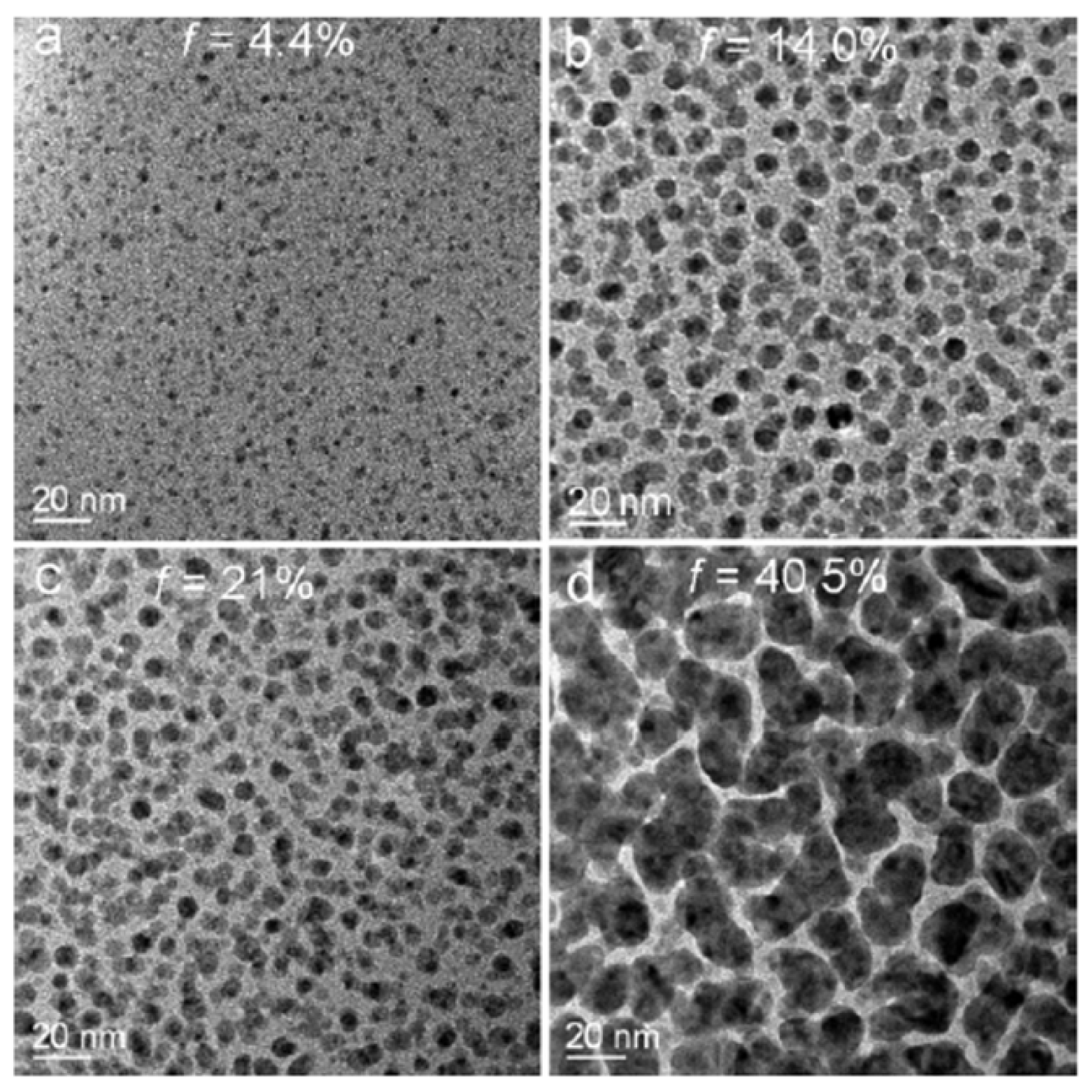
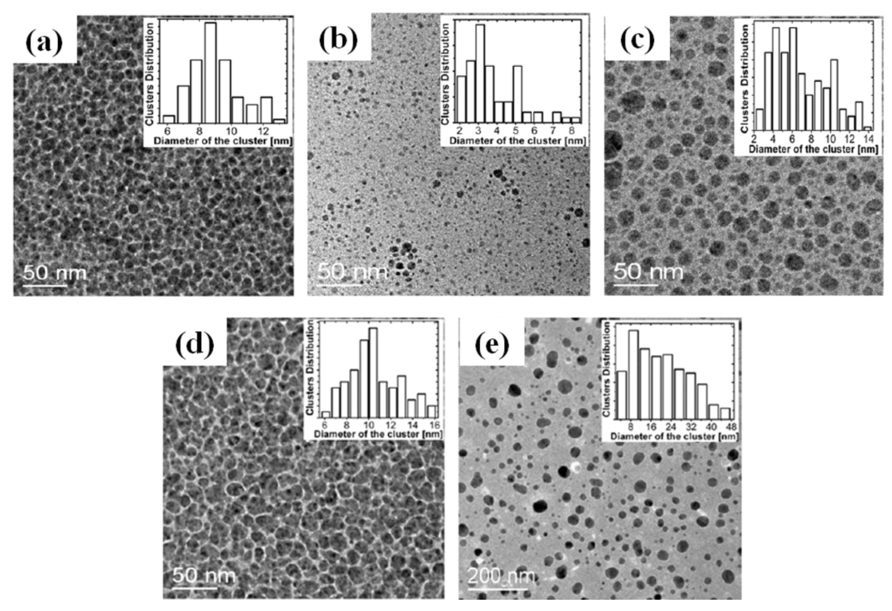
2.2. Polymer Films with Metal Nanoparticles by Co-Deposition Procedures

A well-established method to produce metal NPs/polymer composites is the co-depositions of polymers and metals [9,42,43,44,45,46,47,48,49,50,51,52,53,54]. Co-evaporation and co-sputtering of a metal and of an organic component have been reported to produce functional polymer composites containing metal NPs. This approach allows a fine control, in a wide range, of the metal filling factor, filling factor profile, and composition of the particles. Exploiting such methodologies, several types of metal–polymer nanocomposites were produced with interesting physical properties for functional applications: Ag NPs embedded in polyethylene terephthalate for optical applications [42], Fe-Ni-Co NPs and nano-columns embedded in Teflon AF for magnetic-based applications [44,45], Ag NPs embedded in a polymer matrix of Teflon AF for plasmonic-based applications [46], Ag NPs embedded in polytetrafluoroethylene for electrical and optical applications [47], Au and Ag NPs embedded in Teflon AF and Nylon matrices for electrical applications [48], Ag-Au and Ag-Cu alloy NPs in Teflon AF matrix for plasmonic-based applications [49,50], Au and Ag NPs embedded in polytetrafluoroethylene for antimicrobial applications [54].
In general, during co-deposition of metals and polymers on a substrate, metallic NPs grow by self-assembly processes identical to those involved in the metal cluster formation onto a polymer surface [30,31,45]. This fact arises from the metal higher cohesive energy with respect to that of the organic component and of the very low interaction energy between the two components. So, during the NPs’ formation in the polymer matrix, adsorption and reemission of atoms and molecules, surface diffusion, nucleation and agglomeration occur. In particular, within their diffusion distance, metal atoms may encounter each other or may be bonded by surface defects leading to aggregation and formation of metal clusters which are embedded into the polymer matrix during the growth of the nanocomposite film. In addition, however, the formation of metal NPs in a matrix of simultaneously growing polymer is affected by the sticking coefficient of the metal atoms during deposition [32,46]. The main structural parameter of the metal–polymer nanocomposite film, determining its physical properties (i.e., optical, electrical, etc.) is the volume metal filling factor f [44,45,46,47,48,49,50]. It can be defined as [47]
f = m V ρ p ρ m ρ p
where ρp is the density of the polymer host, ρm is the density of the metal, m and V are the mass and the volume of the composite film. For example [47,48], the properties of the composite film close to the metal percolation threshold change dramatically over a narrow range from a polymer-like to a metal-like material. At low metal concentration, within the polymeric film, isolated particles are present so that the composite film behaves like an insulator. With increasing metal content, the metal clusters spacing decreases, so that the electron tunnelling between neighbouring clusters and the formation of metal chains and conducting paths through the composite material occur and this results in a resistivity decrease of the composite film. The metal volume filling factor has also an important effect on the optical response of the metal–polymer nanocomposite system. As an example, Figure 8 shows UV-Vis spectra of Ag/polytetrafluoroethylene nanocomposite systems at increasing values of the metal volume filling factor f: the shift of the absorption maxima with increasing f is clearly recognizable.
Figure 8. UV-Vis spectra of Ag/polytetrafluoroethylene nanocomposite systems at increasing values of the metal volume filling factor f. The inset indicate the metal volume filling factor value. (Reproduced with permission from [47], Copyright IOP Publishing 2005).
Coatings 05 00378 g008
The metal filling factor depends on the condensation coefficient of metal atoms on a given polymer surface as well as on the metal-polymer deposition ratio [32,45,51]. This means that f can be tuned by the ratio of the deposition rates of metal and polymer [51]. For example, Figure 9 reports transmission electron microscopy (TEM) images of co-evaporated (at room temperature) Nylon (60 nm-thick)/Ag nanocomposites at various metal filling factors: (a) 4.4%, (b) 14%, (c) 21% and (d) 40.5% [51]. As the Ag concentration increases from4% to 50% in the composite, the average size of the Ag NPs in the composite also increases from 2 to 20 nm. Correspondently, also, the NPs morphology changes from spherical to elongated due to the occurrence of the NPs’ coalescence process.
Obviously, also the substrate temperature during co-deposition has a great influence on the nucleation and growth of the metallic NPs in the polymer matrix. It influences, particularly, the microstructures (size, size distribution and inter-cluster separation) of the composite film [46]. For example, Figure 10a–c reports TEM micrographs of Ag-Teflon nanocomposites prepared at different substrate temperatures during deposition (room temperature (a), 90 °C (b), 240 °C (c)) [46]. The insets show the corresponding size distributions. The mean diameters of the clusters are 9.0 nm, 3.8 nm and 7.0 nm, respectively. As previously stated, the metal volume filling factor in the composite is dependent on the condensation coefficient of the metal atoms on the polymer surface during co-deposition.
Figure 9. TEM images of of Nylon/Ag nanocomposites at various metal filling factors: (a) 4.4%, (b) 14%, (c) 21% and (d) 40.5%. (Reproduced with permission from [51], Copyright IOP Publishing 2006).
Coatings 05 00378 g009
Figure 10. (a–c) TEM images of Ag-Teflon films co-deposited at different substrate temperatures. (a) Room temperature, (b) 90 °C, (c) 240 °C. The insets show the corresponding size distributions. The mean diameters of the clusters are 9.0 nm, 3.8 nm and 7.0 nm, respectively. (d)–(e) TEM micrograph of Ag-Teflon as deposited at room temperature (d) and after annealing at 200 °C for 2 min (e). The insets show the corresponding size distributions. The mean diameters of the clusters are 10.5 nm and 21.6 nm. (Reproduced with permission from [46], Copyright IOP Publishing 2008).
Coatings 05 00378 g010
In the case of Ag atoms on Teflon AF, the room-temperature metal adatoms’ condensation coefficient is very small [46] and it decreases increasing the substrate temperature. Above 140 °C it increases again since the polymer is near its glass-transition temperature (160 °C for Teflon AF). The minimum value of the condensation coefficient is due to the competition of thermal desorption and diffusion controlled nucleation processes. Below the glass transition temperature, the reemission of adatoms due to thermally activated desorption increases with increasing temperature resulting in the decrease in cluster density and size of the clusters. Above the glass transition temperature, the growing polymer matrix acts as a viscous fluid enhancer, so the mobility of metal adatoms on the growing polymer surface increases. So, on the high temperature substrate, the adatoms acquire enough energy to grow into larger clusters. The higher the temperature of the substrate during the co-evaporation process, the larger the mean distance between the clusters formed due to the faster surface diffusion of the metal atoms which leads to less nucleation and faster growing clusters. Figure 10d,e shows, also, TEM images of Ag NPs in Teflon AF prior to (d) and after (e) heat treatment at 200 °C in air [46]. Upon annealing the cluster size increases and the cluster density decreases due to a cluster coalescence process.

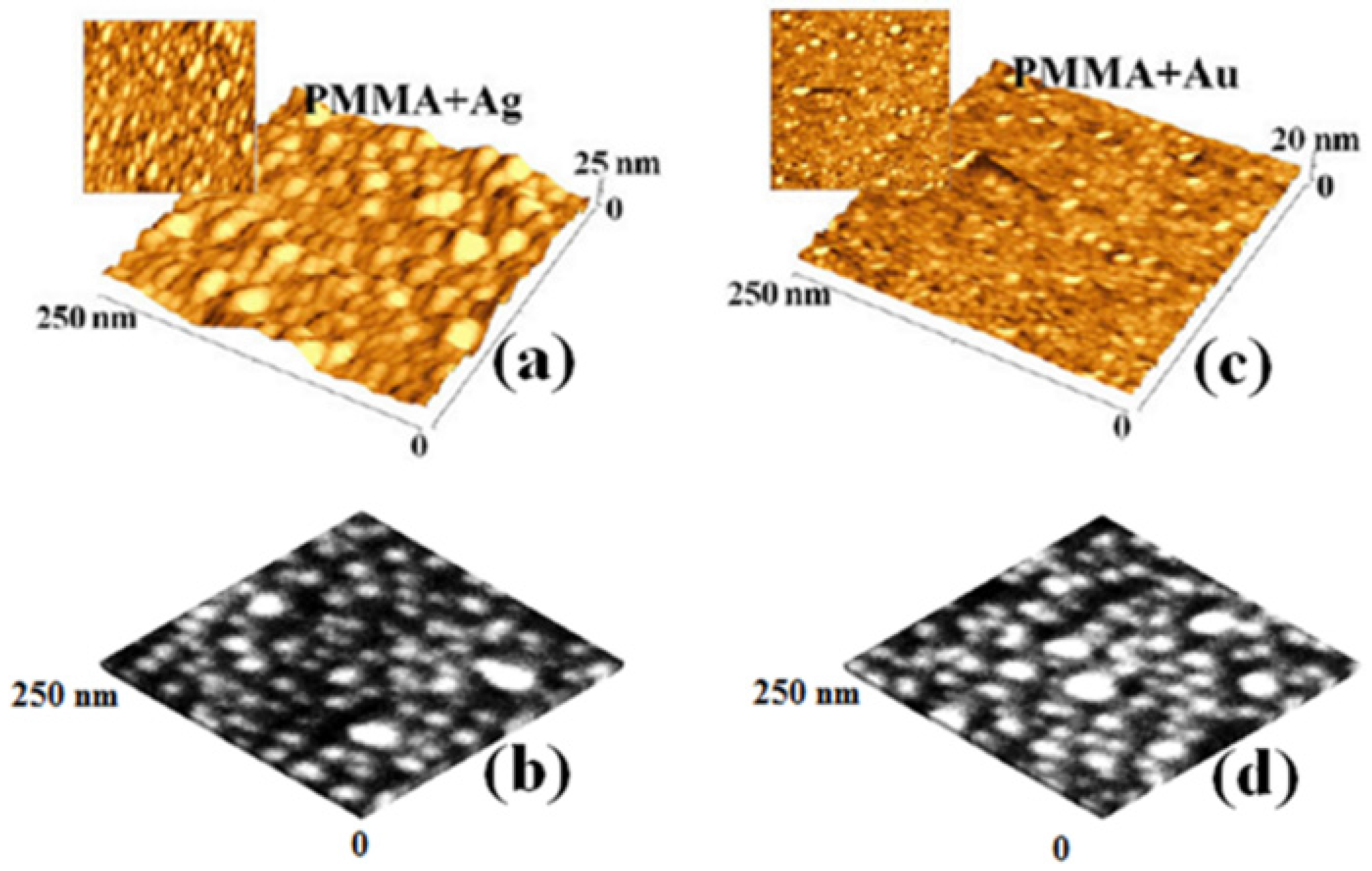
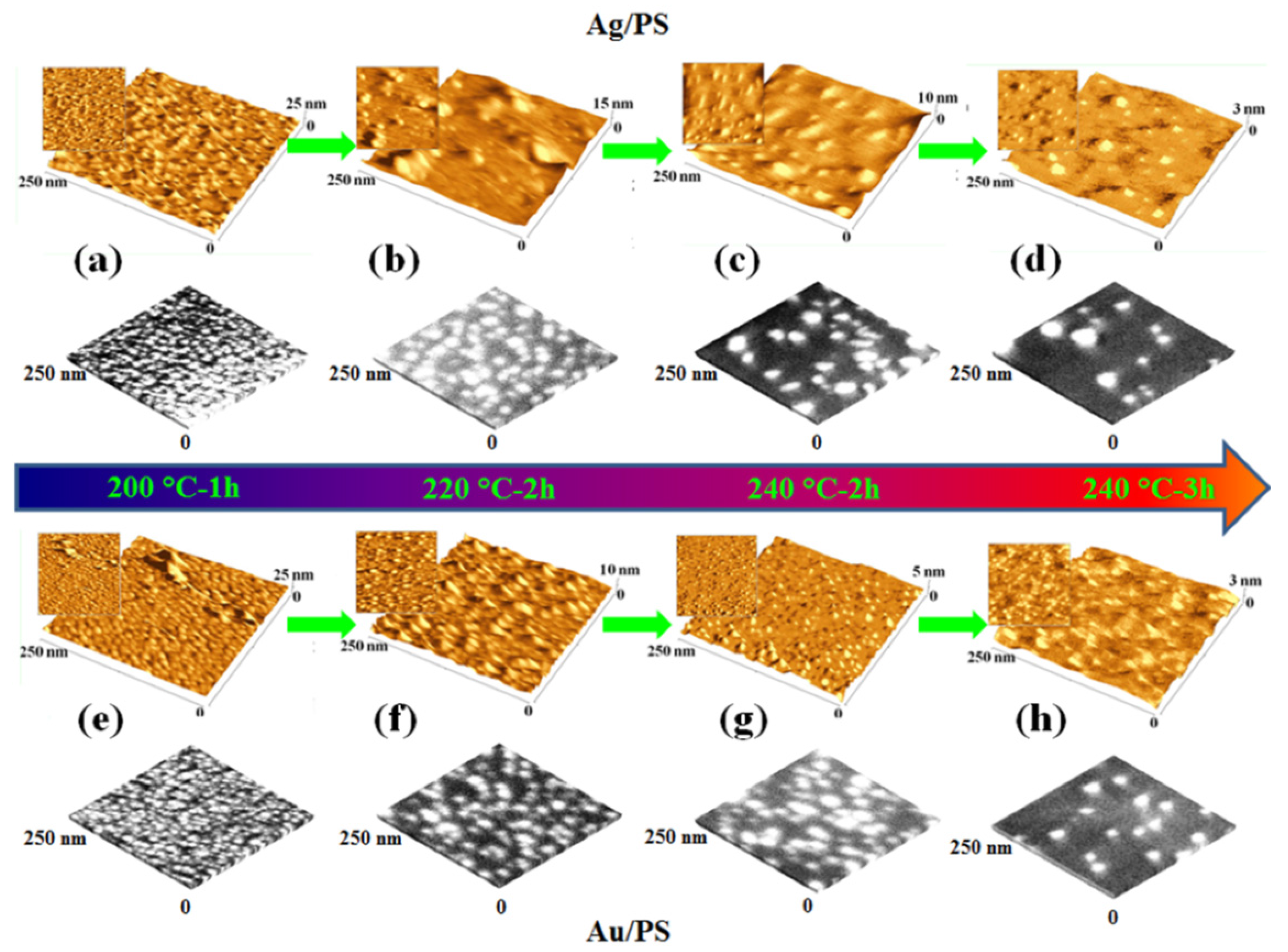
2.3. Polymer Films with Embedded Metal Nanoparticles Exploiting the Embedding Phenomenon

A method, alternative to metals and polymers co-deposition processes, to produce polymer-metal nanocomposite films is based on the embedding phenomenon of metal NPs deposited on the polymers surface [27,30,31,55,56,57,58,59,60,61,62,63,64,65]. For example, in fact, first the polymer can be spin-coated on a substrate and the thickness of the polymer layer can be controlled by the process parameters (rpm, etc.); then, during the metal evaporation or sputtering depositions on the polymer surface, the starting mean NPs size and surface density can be controlled by the process parameters (power, time, etc.); finally, when following the annealing process above the polymer glass transition temperature, the fraction of embedded NPs can be controlled by the annealing time and temperature. So, overall control of the metal fraction volume can be obtained.
The metal NPs’ embedding process into the polymer layer can be understood on the basis of surface free energy considerations: the Gibbs free energy of a metal NP inside a polymer is lower than that of the NP at the polymer surface [55,56]. So, the Gibbs free energy minimization of the system is the driving force for embedding of metal-NPs in polymers. In particular, the surface Gibbs free energy is effectively reduced by NPs embedding if γm > γp + γMP being γm the metal surface tension, γp the polymer surface tension, and γmp the metal–polymer interfacial tension [55,56]. This condition is, usually, fulfilled for metal NPs on a polymer given the fact that metals have surface energies two orders of magnitude higher than the polymers. Some research groups have used scanning probe microscopy [58,65], X-ray reflectivity [60,61] and X-ray photoelectron spectroscopy [63] to study the embedding of metal NPs in polymers. Some studies highlighted a complete embedding of the metal NPs in the polymeric layers [55,56,61,62], while others analyses highlighted only partial embedding [58]. Such a difference is related to the dependence of the embedding process on the polymer chain mobility: so, partial or no embedding can be expected at temperatures below the polymer glass-transition temperature Tg, while NP complete embedding is observed at temperatures higher than Tg [62]. Deshmukh et al. [64] studied, using transmission electron microscopy, individual Au NP embedding in a polystyrene melt showing that the NPs near the polymer surface are completely covered by a thin wetting layer of polymer with critical thickness d*. They claimed that the metal NP embedding process in the polymer layer starts thanks to the capillary pressure that results from the curvature of the wetting layer determining the complete embedding of the NP into the polymer. According to their observations, the critical thickness d* is the equilibrium film thickness for the spreading of the polymer melt on the metal substrate.
To study the kinetics characteristics of the embedding process of metal NPs in polymeric layers, we report, here, some results and considerations about Au and Ag NPs embedding in polystyrene (PS) and poly(methyl methacrylate) (PMMA) [65]. The PMMA and PS glass transition temperatures Tg and melting temperatures TM are, respectively, 105 and 160 °C (PMMA), and 95 and 240 °C (PS) [66]. So, the experiments consisted, firstly, of the formation of Au or Ag NPs on PMMA or PS substrates, by Au or Ag sputtering depositions. Then, the Au NPs/PMMA and Ag NPs/PMMA composites were annealed at 120, 140, and 160 °C in the 60–180 min time range, while the Au NPs/PS and Ag NPs /PS composites were annealed at 200, 220, and 240 °C in the 60–180 min time range.
Figure 11 and Figure 12 report atomic force microscopy (a–c) and scanning electron microscopy (b–d) images of 10 nm-thick Ag and Au films sputter-deposited (at room temperature) on the PS and PMMA layers. Figure 13 and Figure 14 report two-dimensional and three-dimensional reconstructions of 0.25 μm × 0.25 μm atomic force microscopy and scanning electron microscopy images of the Ag/PS and Au/Ps (Figure 13), Ag/PMMA and Au/PMMA (Figure 14) systems for some annealing temperatures and times. For each sample, by a direct visual inspection of the images sequences, a clear feature can be recognized: the decrease of the mean NPs height and of the number of NPs, increasing the temperature and/or time of the thermal process. These aspects can be inferred observing the decrease of the height scale in the AFM images and the decrease of the bright regions in the SEM images increasing the annealing temperature or time.
Figure 11. Representative two-dimensional and three-dimensional reconstruction of 0.25 μm × 0.25 μm AFM images of Ag (a) and Au (c) films deposited on PS. (b) and (d) report the correspondent SEM images. (Reproduced with permission from [65], Copyright Springer 2012).
Coatings 05 00378 g011
Figure 12. Representative two-dimensional and three-dimensional reconstruction of 0.25 μm × 0.25 μm AFM images of Ag (a) and Au (c) films deposited on PMMA. (b) and (d) report the correspondent SEM images. (Reproduced with permission from [65], Copyright Springer 2012).
Coatings 05 00378 g012
Figure 13. Representative two-dimensional, three-dimensional 0.25 μm × 0.25 μm AFM and SEM images of Ag (a)–(d) and Au (e)–(h) films deposited on PS and annealed for various temperatures and times. (Reproduced with permission from [65], Copyright Springer 2012).
Coatings 05 00378 g013
Figure 14. Representative two-dimensional, three-dimensional 0.25 μm × 0.25 μm AFM and SEM images of Ag (a)–(d) and Au (e)–(h) films deposited on PMMA and annealed for various temperatures and times. (Reproduced with permission from [65], Copyright Springer 2012).
Coatings 05 00378 g014
Using the AFM analyses, the mean NPs height <h> can be evaluated. Using both AFM and SEM analyses, the NPs’ surface density N (particles/cm2) can be evaluated. So, Figure 15a,b reports: the evolution of <h> (a) and the evolution of the number NE of missing NPs (calculated as the differences between the starting number of NPs in the as-deposited sample (N(t = 0)) and the number of NPs after the thermal process (N(T,t)) for all the samples, for each annealing temperature T, as a function of the annealing time t. We can infer that the decrease of <h> and increase of NE when T or t increase univocally indicate the occurrence of an embedding process of the Au or Ag NPs into the PS or PMMA. This is possible thanks to the long-range polymeric chain mobility above the glass transition temperature. In Figure 16 this process is pictured.
After the preliminary step in which the NP near the polymer surface is coated by a wetting layer of critical thickness d* (about 1.3–1.8 nm for the case of Au NP embedding in a PS melt, Figure 17 [64]), the capillary pressure that results from the curvature of the wetting layer drives the complete embedding of the NP into the polymer.
In Figure 16a, the temporal region in which <h> is constant indicates the characteristic time needed for a thin wetting layer of the polymer to coat the metal NPs. We call this characteristic time t0 (3230 s in this case) the “coating time”. After this characteristic coating time, the embedding process of the NP into the polymer occurs. In this embedding stage, <h> decreases linearly with the annealing time so that the characteristic embedding velocity v can be evaluated (v = 2.3 Å/min. in the case shown in Figure 16a. Figure 18 reports the Arrhenius plots for the evaluated embedding velocities (dots): ln(v) decreases linearly with 1/T (T the absolute temperature) and the typical Arrhenius relation v = v0exp(−EA/kT) (v0 the pre-exponential factor, k the Boltzmann constant, T the absolute temperature, EA a characteristic activation energy for the embedding phenomenon) is used to fit (full lines) the experimental data allowing to evaluate, in particular, EA(Ag/Ps) = 390 ± 20 meV, EA(Au/Ps) = 400 ± 20 meV, EA(Ag/PMMA) = 230 ± 30 meV, EA(Au/PMMA) = 220 ± 20 meV.
Figure 15. (a) Evolution of the mean NPs height <h> as a function of the annealing time t for each fixed annealing temperature T for the investigated systems. (b) Evolution of number NE of the embedded NPs as a function of the annealing time t for each fixed annealing temperature T for the investigated systems.
Coatings 05 00378 g015
Figure 16. Evolution and sketch of the correlation between the evolution of <h> vs. t and the embedding process stages. The particular case of Au/PS at 513 K is taken as an example. (Reproduced with permission from [65], Copyright Springer 2012).
Coatings 05 00378 g016
Figure 17. TEM images of gold NP embedding into a polymer melt PS surface upon annealing for three days at 130 °C. Images show (a) a partially embedded NP covered by a wetting layer of polymer, (b) a nearly completely embedded NP near the surface (indicated by the arrow), (c) a completely embedded NP diffused below the surface, and (d) a partially embedded cluster containing six to eight NPs and covered by a wetting layer. The dotted lines in b, c, and d are a guide to the eye to denote the polymer surface. (Reproduced with permission from [64], Copyright American Chemical Society 2007).
Coatings 05 00378 g017
Figure 18. Evolution Arrhenius plots of the embedding velocity as a function of the annealing temperature T for the Ag/PS and Au/PS (a), Ag/PMMA and Au/PMMA (b) systems. The full lines are the exponential fits of the experimental data. The values obtained for the activation energy are indicated. (Reproduced with permission from [65], Copyright Springer 2012).
Coatings 05 00378 g018

3. Electrical Properties of Metal-Polymer Nanocomposites

In the framework of the nanotechnology revolution, metal–polymer nanocomposites have become a key area of current research and development because of their technological applications [8,67,68,69,70]. Polymers are interesting host matrices for embedding metal NPs as they act as reducing and capping agents and, additionally, provide environmental and chemical stability [71,72]. So, metal-polymer nanocomposites often exhibit improved optical, electrical, thermal and mechanical properties (with respect to those of the single components) [73,74]. In this sense, several literature works report on the attempts for the controlled fabrication of metal NP based polymer nanocomposites, whose aim is the control of variation in their optical and electrical properties for their application in high performance capacitors, conductive inks, opto-electronic, electrical and optical devices, biomedical science, sensors, etc. [75,76,77,78,79]. Key steps towards real technological applications are: selection of polymer–metal NP combinations, controlling the particle size, and their concentration and distribution within the polymer matrix [77,78,79].
On the basis of these considerations, in the following we review properties of nanocomposite films composed of: (1) metal NPs deposited on polymeric films, (2) metal NPs co-deposited with polymer film and of (3) metal NPs embedded in polymeric film. Finally, particular attention is devoted to conducting polymer based nanocomposite films and their technological applications.

3.1. Bilayer or Multilayers Systems

Polymer-based layered nanocomposite systems can be used to fabricate tunable electronic devices exploiting the interaction characteristics between the layers forming the systems. An exemplificative case is that related to the tunable barrier height of Metal/Semiconductor (MS) Schottky contacts when polymer/metal layered systems are inserted between the metal and semiconductor [80]. For example, Torrisi et al. [80] studied the electrical performances of the standard Au/Si Schottky contact when Hybrid multilayers (HyMLs) composed of PMMA/Au NPs or P3HT/Au NPs are inserted between the Si and the Au. In particular, they demonstrated that the Au/Si barrier height can be widely tuned changing the polymer nature (PMMA or P3HT, in the specific case) and the number of polymer/Au NPs inserted layers. First of all, they developed an iterative mixed wet chemical (spin-coating for the polymers deposition)/dry physical (sputtering for the Au NPs deposition) fabrication method involving the sequential depositions of the polymers and Au NPs films. A scheme depicting the fabricated Au/Si Schottky device with the inserted HyMLs is shown in Figure 19.
The sequence polymer/Au NPs is named 1 bilayer (BL), the sequence polymer/Au NPs/polymer is named 1.5 BL, the sequence polymer/Au NPs/polymer/Au NPs is named 2BL and so on. The current-voltage (I-V) characteristics of the modified Au/Si Schottky devices were acquired and studied, as a function of the BLs’ number N, for as-deposited and annealed (at temperature higher than the polymer glass transition temperature: 150 °C for 60 min for the PMMA based samples and 230 °C for 30 min for the P3HT based ones) samples. For example, Figure 20 shows I-V characteristics, respectively, for Au/(PMMA/Au NPs MLs)/Si, before (a) and after (b) annealing, and for Au(P3HT/Au NPs MLs)/Si, before (c) and after (d) annealing. In particular, I-V curves for the Au/Si (reference), 1.5, 3.5, and 5.5 BLs samples are reported.
Figure 19. (a) Schematic representation of polymer/metal bilayer; (b) Au/HyMLs/p-Si Schottky device together with the current-voltage (I-V) configuration setup. (Reproduced with permission from [80], Copyright AIP Publishing LLC 2013).
Coatings 05 00378 g019
Figure 20. I-V measurements of as dep (a) and annealed (b) HyMLs PMMA/Au NPs; as deposited (c) and annealed (d) HyMLs P3HT/Au NPs. (Reproduced with permission from [80], Copyright AIP Publishing LLC 2013).
Coatings 05 00378 g020
These characteristics are analyzed within the standard thermo-ionic emission framework to extract the devices barrier height (BH) ΦB and ideality factor n as a function of the N before and after the annealing. So, Figure 21 reports the plots (dots are experimental data and lines are fits or guides for the eyes) of ΦB and n as a function of N for as deposited and annealed PMMA/Au ((a) and (c)) and P3HT/Au ((b) and (d)) HyMLs, respectively. From Figure 21a,b, Torrisi et al. argue that BH of the Au/p-Si contact is ΦB = ΦAu/Si = 0.71 ± 0.02 eV and the insertion of the single polymer layer increases this value to ΦAu/PMMA/Si = 0.79 ± 0.02 eV and to ΦAu/P3HT/Si = 0.76 ± 0.02 eV. Increasing N, a linear decrease of ΦB can be observed for the as-deposited samples. Instead, the annealed samples exhibit a constant value of BH very close to ΦB = ΦAu/Si = 0.71 ± 0.02 eV. In addition, the device ideality factor n (Figure 21c,d) increases when N increases for the as deposited samples, while it is constant with N for the annealed samples.
Figure 21. Graphics of barrier height vs. number of bilayers for as deposited and annealed PMMA based HyMLs (a) and for P3HT based HyMLs (b). Graphics of ideality factor vs. number of bilayers for as deposited and annealed PMMA based HyMLs (c) and for P3HT based HyMLs (d). (Reproduced with permission from [80], Copyright AIP Publishing LLC 2013).
Coatings 05 00378 g021
Torrisi et al. discussed the previous experimental behavior on the basis of the following general consideration: the insertion of an insulator film between metal and semiconductor of a Schottky device modifies the standard thermoionic I-V equation in the saturation current factor as per [81]
I 0 = A A * T 2 exp [ q ( Φ B + Φ 0 ) / k T ]
with A the diode area, A* the semiconductor Richardson constant, T the absolute temperature, q the electronic charge, k the Boltzmann constant, ΦB the Metal/semiconductor characteristic barrier height and Φ0 an additional term which is the barrier height introduced by the insulating layer. In particular, Φ 0 = χ e 1 / 2 δ where χ e = 2 ( 2 m n χ c ) 1 / 2 / , δ the barrier thickness, mn the effective tunneling mass of electrons, χc the effective barrier height presented by the thin interfacial layer, ħ the reduced Planck constant. On the basis of this consideration, so, starting from the simple Au/p-Si contact having an experimental barrier height ΦB = ΦAu/Si = 0.71 eV, the insertion of a polymer layer (PMMA insulating or P3HT semi-insulating) leads to the increase of device barrier height by an effective amount ΦP, while the insertion of the Au NPs layer leads to the decrease of the device barrier height by an effective amount ΦAu. So, we can think in Equation (5) that Φ0 = ΦP + ΦAu being ΦP > 0 and ΦAu < 0. Then, the data ΦB vs. N for the case of the PMMA/Au NPs HyMLs insertion before annealing treatments are obtained when ΦP = ΦPMMA = 0.08 ± 0.01 eV and ΦAu = −0.11 ± 0.03 eV. After the annealing process of the device, Figure 21a shows ΦB ≈ 0.71 eV independently of N (red dashed line is a guide for eyes) that is the value of the Au/p-Si contact. This fact suggests them that the annealing process causes the Au/PMMA mixing [65,82] (due to the increased polymeric chains mobility above the polymer glass transition temperature) so that metal percolation paths are generated between the bottom Si and the top Au contacts. The same approach applied to the P3HT/Au NPs HyMLs insertion case, Figure 21b, leads to ΦP = ΦP3HT = 0.05 ± 0.01 eV and ΦAu = −0.08 ± 0.02 eV before the annealing process of the device. Finally, the increase of n with N for both (PMMA and P3HT) the as-deposited samples, with respect to the 2.8 value for Au/Si diode, is, however, the clear indication of the progressive lack of uniformity at Au/Si interface due to the addition of Au and polymeric layers. In contrast, the constant value of n for the annealed samples is in agreement with the possible annealing-induced metal percolation paths formation between the Au top contact and p-Si back contact.
The data discussed in this section highlight the versatility of the polymer-metal nanocomposite layered systems in the wide-range tuning of the electrical response of key electronic device components.

3.2. Metal Nanoparticles Co-Deposited with Polymer Film

The electrical properties of nanocomposites composed of metallic NPs dispersed in a polymer matrix can be tuned from the polymer ones to the bulk metal ones by controlling the metal filling factor and the matrix structure [83]. In general, in a nanocomposite system formed by metal NPs embedded in insulator polymeric films, three different conduction regimes can be obtained, on the basis of the film composition: the dielectric, transition, metallic regimes [84]. The dielectric regime is obtained at low metal filling factor: in this case, small, isolated metal particles are dispersed in the dielectric polymeric film. The metallic regime is obtained at filling factor higher than the critical value for the metal particles percolation: in this case, the metal particles come into contact and give way to a metallic continuum with dielectric inclusions. In the transition regime, the structural inversion between the dielectric and the metallic regime occurs.
For example, Takele et al. [47,48] focused their attention on the electrical properties of nanocomposite films with embedded Ag and Au NPs in different polymer matrices (Nylon 6, Teflon AF 1600, PTFE) which are prepared by co-deposition of metal and polymer. Figure 22 reports, as an example, the resistivity of thin PTFE films with embedded Ag NPs as a function of metal filling factor f [47]. From such a plot, the three different resistivity regions are clearly recognizable. In particular, the transition region from the high-resistivity behavior to the low-resistivity behavior takes place in correspondence with a critical value of f named the percolation threshold fc [8,85]. At fc, an insulator to metal transition of the composite film occurs: the value of the electrical resistivity changes from 105 Ωm below fc to 10−5 Ωm above fc. This drastic change in resistivity of the composites at the percolation threshold is related to the fractal geometry of the infinite metal NP in the polymer matrix [86,87]. At f = fc, the assumption of a random resistance network model, dictates that all current flows through a single metal particle providing the connection between the electrodes. However, the percolation threshold is not determined only by the chemical composition of the composite material but depends, also, on the structure of the aggregates and on the ratio between the conductivities of the metallic and insulator phases. So, the measure of the electrical resistivity of Ag-Teflon AF, Au-Teflon AF, and Au-Nylon, indicates, often, the effect of the microstructure on the percolation threshold [48].
Figure 22. Change of the electrical resistivity of thin PTFE films with embedded Ag NPs with increasing filling factor. (Reproduced with permission from [47], Copyright IOP Publishing 2005).
Coatings 05 00378 g022
Near the percolation threshold the drastic change in the nanocomposite polymer/metal film conductivity with a small change in the film structure make difficult the detailed experimental study of the system electrical transport properties by d.c. (direct current) conductivity measurements only. Due to the influence of the film microstructure on the percolation threshold, the filling factor alone is, often, not sufficient for a complete characterization of the electrical properties of the nanocomposite film. For example, these electrical properties are strongly dependent on the metal NP spacing [88]. A NP’s size variation (3–15 nm) and inter-distance change (2–20 nm) is manifested between the dielectric and metallic regime of a nanocomposite changing the metal filling factor. Such orders of magnitude determine very high values of the internal electrical field between the metal NPs: typically, when a voltage of 1 V is applied between the electrodes, internal fields up to about 106 V/cm in the dielectric regime and 107 V/cm in the metallic regime can be induced between the metallic particles. With these high electrical field values, the electron in the metal NPs can acquire enough energy to be emitted from the metal by a field emission process [89]. So, typically, the electrical transport between metal NPs embedded in insulating polymeric films involves an activated electron tunneling between metal particles separated by potential barriers. The characteristic activation energy of the process is determined by electrostatic image forces. The δEF energy required to remove an electron from a metallic particle to a neighboring one [90,91] can be approximated by
δEF = (e2/εε0)[(1/r)−(1/s)]
where e is the electronic charge, ε and ε0 are the dielectric constants of the matrix and vacuum, r is the particle radius, and s the spacing between the particle centers. In addition to the tunneling process, the electron conduction can take place via hopping from defect to defect in the insulator.
Takele et al. [48] applied these concepts to discuss the experimental current-voltage characteristics of Au-Teflon AF nanocomposites as a function of the Au filling factor f. According to their data and discussion, at f = 0.36, well below the percolation threshold, the Au particles in the dielectric matrix are separated by a large distance from each other and the induced electric field is not sufficient to promote the electron tunneling transport from NP to NP. Above the percolation threshold (f > 0.42), the Au NPs form a metallic continuum with dielectric inclusions: now, the induced field is high enough (since the interparticle separation is small) to make the electrons’ field emission mechanism the dominant one. So, the experimental I-V characteristics of Teflon AF composites determined by Takele et al. show a different behavior for various Au concentrations. In particular, the slope of the I-V curves showed an increase with increases in the metal filling factor up to a certain voltage (at f < fc, the conductivity caused by the field induced tunneling is very small: the slope of the I-V curves is low; at f > fc, the electrical field induced across the electrodes is large enough to cause the electrons to tunnel from one cluster to a neighboring one: the slope of the I-V curves is high).
Furthermore, Takele et al. [48] reported on the electrical resistance of the Au/Teflon AF composites as a function of the annealing temperature for samples below and above the percolation threshold. The shape of the curves in both cases is not similar, which indicates that their electrical conductivity mechanism is quite different from one another. Similar effects have been reported also for different polymer composites [92,93]. For example, Takele et al. [48] reported, also, electrical conductivity measurements from the room temperature to 180 °C for Nylon composites with various Au concentrations. Similarly to the previous case, the resistance versus temperature plots showed different behaviors for samples characterized by Au concentration below and above the percolation threshold. At f < fc, a post-deposition annealing process promotes the coalescence of the Au NPs into larger particles more distant from each other. As a consequence, an increase in the sample resistance is observed up to a critical temperature Tm. On the contrary, for T > Tm (T the annealing temperature), a sample resistance decrease is observed and it is attributed to a rearrangement process of the metal NPs. At f > fc, the post-deposition annealing process determines the formation of a more conductive path between the electrodes causing a drastic drop in the sample resistivity at T = Tm. To complete this analysis, Takele et al. [52] compared also the electrical properties of nanocomposite films formed by Au nanoparticles embedded in Teflon AF and Poly(α-methylstyrene). The metal percolation threshold was identified in 0.43 and 0.20 for Au in Teflon AF and Poly(α-methylstyrene), respectively. The composite films deposited with varying filling factors showed large variations in conductivity and optical behaviour. For a composite with relatively low f, spherical metal particles inside the polymer matrix are distributed uniformly without the formation of a continuous network. At higher f, an aggregate structure containing a random mixture of the metal and polymer is observed. As already discussed, the character of electrical transport depends on the film composition and the separation between NPs [90,94]: at the percolation threshold there is an abrupt change in the resistance from the insulation to the conductance regime [95], see Figure 23 [52]. The resistance of the Au-TAF nanocomposite films drops by several orders of magnitude at a metal volume fraction f = fc = 0.43. The same behavior is presented by the Au- P(α-MS) composite with fc = 0.2 [52]. However, while the fc = 0.43 value for the Au-TFA is in agreement with several theoretical predicted values for the percolation threshold for spherical clusters (ranging between 0.28 and 0.5 [96,97]), the 0.2 value for the percolation threshold of the Au- P(α-MS) is outside the predicted range and can be attributed to general morphology variations of the nanocomposite with respect to that imposed in the theoretical calculations.
Figure 23. Change of electrical resistance with increasing filling factor of Au-TAF nanocomposites. (Reproduced with permission from [52], Copyright Cambridge University Press 2006).
Coatings 05 00378 g023

3.3. Metal Nanoparticles Embedded in Polymer Film

In this section, representative electrical properties of nanocomposite films formed by metal NPs embedded in polymeric matrices and obtained by soft chemical approaches are discussed. The aim is to highlight the key similar and different aspects with the electrical properties of metal NPs embedded in polymers and obtained by co-deposition methods discussed in the previous section.
Mahendia et al. [98] fabricated Poly(vinyl alcohol)-silver (PVA-Ag) nanocomposite films by the soft chemical route. The effect of the concentration of embedded Ag NPs on the film conductivity and on the films dielectric relaxation behavior was analyzed. In particular, when increasing the Ag NPs’ concentration from 0 to 1.32 wt %, the nanocomposite dc conductivity was found to increase from 1.38 × 10⁻¹¹ to 9.17 × 10⁻¹¹ S/cm. Correspondingly, the film dielectric constant was found to decrease from 1.74 to 1.07 at a frequency of 75 kHz. In addition, the authors, evaluated, from dielectric data, the nanocomposite ac conductivity and polarization relaxation time. Also, these data corroborate the enhanced conductivity of PVA matrix with increases in the Ag NPs’ concentration. Figure 24 summarizes the authors’ results [98]: it reports the dc electrical conductivity of the samples with increasing the Ag NPs concentration (0.13, 0.26, 0.41, 0.50, 0.80 and 1.32 wt %), showing that the conductivity of PVA increases by 1 order of magnitude when the Ag concentration reaches 1.32 wt %. The authors attribute such a behavior to the production of charge transfer complexes (CTCs) in the polymer chain network caused by the Ag NPs embedding, whereas the Ag is regarded as a dopant element. In fact, dopant elements introduced in semi-crystalline polymers determine, by the formation of CTCs, the decrease of the barrier height between the trapping sites for the charge carriers. So, conducting paths through the amorphous regions of the polymer matrix are obtained resulting in the conductivity increase of the metal-doped polymer [99]. Consequently, also, a decrease of the charge transport activation energy and an increase of the charge carriers’ mobility is expected. In the specific case of the Ag/PVA system, therefore, the authors suppose that Ag NPs fill the free volume holes (amorphous phase) and occupy the interstitial positions between the polymer chains in amorphous phase. The NPs link these chains to some kind of bonds by charge exchange process between the Ag NPs (the dopant) and PVA chain network. Since the extent of complexes’ formation increases with doping element concentration, both the charge carrier density and the Ag/PVA composite conductivity increase.
Figure 24. Variation in dc conductivity (σdc) of PVA-Ag nanocomposites with concentration (wt %) of Ag nanoparticles. (Reproduced with permission from [98]) (Copyright Elsevier 2010).
Coatings 05 00378 g024
Remarkably, the authors noted that the increased charge carriers hopping probability across the barrier and insulator chains, determined by the CTC formation, can also be explained in the framework of the percolation theory (the favored point of view discussed in the previous section): from such a point of view, the Ag NPs act as conductive fillers in the polymer matrix providing the continuous conductive pathways for the transfer of charge from one CTC to another [89,100]. Figure 25a,b report, for the Ag/PVA composite at various Ag concentrations, the frequency-dependent dielectric constant ε′ and dielectric loss ε″, with the measurements performed at the temperature of 307 K.
At each Ag concentration, ε′ decreases with increases in the frequency f. This is true also at zero concentration (pure PVA) where ε′ is ~1.74 at frequency 75 kHz and decreases to ~1.02 at 5 MHz [101,102,103]. However, increasing the Ag concentration, lower and lower values of εʹ are obtained. Similar behavior is reported for several others metal-doped polymer films (PVP, PMMA, etc.) suggesting that for polar materials, the value of εʹ is high for low frequency range and decreases as frequency increases [104,105,106]. The reason for this behavior is identified in the electrode and interfacial effects of the sample: at low frequency, electrical dipoles in polymeric samples tend to orient themselves as the applied external electrical field; in the high frequency regime, on the basis of polarization effects, the electrical dipoles in polymeric samples have a very small tendency to orient as the external applied electric field and then for field increase at high frequencies, the dielectric constant decreases [107]. Figure 25a shows also the decrease of ε’ with increases in the Ag concentration: this is the direct result of the increased PVA dc conductivity increasing the Ag concentration.
Figure 25. (a) Variation in dielectric constant (ε′) with frequency for different concentration (wt %) of Ag nanoparticles in PVA. (b) Variation in dielectric loss factor (ε″) with frequency for different concentration (wt %) of Ag nanoparticles in PVA. (Reproduced with permission from [98], Copyright Elsevier 2010).
Coatings 05 00378 g025
Concerning the behavior εʹʹ with frequency (Figure 25b), we can observe its decrease with increasing frequency f. In the low frequency region, the higher values of ε’’ are attributable to the mobile charges within the polymer matrix. On the contrary, in the high frequency region, the periodic field inversion is so fast to inhibit the excess ion diffusion in the direction of the electric field [104,105]. So, the polarization effect decreases (due to charge accumulation) and, correspondently, ε″ decreases. To conclude, we mention that the authors observed for the Ag/PVA system, the increase of the ac conductivity as the Ag concentration increases. Overall, the authors observe that in PVA, as the bond rotates with frequency, the existing flexible polar groups with polar bonds induce dielectric α-transition. Correspondently, a change in chemical composition of the polymer repeated unit occurs (the CTCs formation), making the polymer chains more flexible, and so both the dc and ac electrical conductivity is increased [99].

3.4. Conducting Polymer Based Nanocomposites and Their Applications

Nanocomposite materials with attractive properties for technological applications (such as catalytic, sensing and opto-electronic) have been obtained, also, through the combination of conducting polymers with metals (either noble or transition metals). These materials are also intricate combinations, up to almost the molecular level, of one or more inorganic nanoparticles with a polymer so that unique properties of the former can be taken together with the existing qualities of the latter.
Due to their versatility, conducting polymers (CPs) and nanostructured CPs are attracting much interest. They are promising candidates to produce hybrid-system based electronic devices exploiting the possibility to tune their electric conductivity between semiconductor-type to metallic-type aging on doping and de-doping processes. Moreover, they provide the solid possibility to fabricate highly efficient photonic devices (e.g., solar cells) with controlled properties from the nanostructured CPs by a bandgap tuning process. In this field of electronic device applications, the nature of the association of the components, the nanoscale structure of the nanocomposite materials and the effects of their morphology are critical points to control their physical properties. Tailoring nanoscale architectures of conducting polymer based nanocomposites is a challenge for materials scientists.
Surely, nowadays, the most used CPs to produce hybrid nanomaterials for sensing and optoelectronic devices are polyaniline (PANI), polypyrrole (PPy) and poly(3,4-ethylenedioxythiophene) (PEDOT) [108]. Unique redox properties of PANI and PPy have lured scientists to utilize them as cathodic materials in rechargeable Li battery, but their poor charge discharge capacity has hampered their successful application in this respect. This limitation could be overcome by incorporating cathode active materials into conducting polymer matrix. PANI, PPy and PEDOT have been used as the supporting matrix in different composites for intercalation of catalytically active nanoparticles so that the catalytic activity can be retained in the composite. Moreover, composite nanomaterials based on these polymers proved to be powerful in sensing, environmental emission control, workplace hazard monitoring, bio-molecular detection thanks to chemical specificities, tunable conductivities, high mechanical flexibilities and low temperature processability [109,110,111,112,113]. Novel network nanocomposites are proved to possess unique charge transfer and electrocatalytic properties, due to the enhanced interfacial interaction between the polymer network and the loaded metallic particles [109,110,111,112,113]. In this framework, the incorporation of metal NPs into CPs and the decoration of nanostructured CPs with metal NPs are considered good methodologies to enhance the sensitivity, response time and stability of chemical sensors and biosensors [114,115,116,117,118]. For example, nanocomposite thin film and nanowires formed by CPs in conjunction with the metal NPs have shown extraordinary chemical and biochemical sensing efficiency in revealing many types of analytes. In synthesis, the increase of the specific area and catalytic efficiency due to the metal NP and CP combinations are the key advantages for metal/conducting polymer as chemisensors and biosensors [116,117,118].
Mainly, the metal/CP based sensors reported can be classified into two categories [112,113,114,115]: (1) the chemiresistive sensors based on the measure of the relative changes in the system resistance upon exposure to various targets; (2) the electrochemical sensors involving the oxidization or reduction of the targets at an electrode to measure the resulting current.
In this section, the two types of sensors for both chemical and bio-chemical analytes are discussed.

3.4.1. Chemiresistive Sensors

Chemiresistive sensors find applications in areas such as healthcare, safety, energy production and so on. The operation of these sensors is based, mainly, on the resistance change of the system due to the interaction with different targets [112,113,114,115]. The sensor’s sensitivity is defined as (RR0)/R0 (usually expressed as a percentage), being R0 the resistance of the sample before exposure to the test gas and R the time-dependent resistance of the sample upon exposure to the test gas. As an example, Shirsat et al. [116] studied the sensitivity of Au NPs functionalized polyaniline (PANI) nanowires to the chemiresistive detection of H2S: while non-functionalized PANI nanowires show no response at H2S concentrations as high as 500 ppm (Figure 26a), Au NPs functionalized PANI nanowires are highly responsive to H2S presence, even as low as 0.1 ppb (Figure 26b). The authors discuss the great change in the resistance of the PANI nanowires-Au NPs composite after the target exposure, invoking the formation of Au-S bonds which enhance the doping level of PANI. So, the Au-PANI behaves as an acceptor–donor pair and transfers electrons from the p-type PANI network determining the decrease of the overall system resistance. Similarly to these observations, Yang et al. [119] reported on the enhancement of the resistance changes (due to exposure to specific gas targets) for PPy nanotubes/Ag composites with respect to the pure PPy nanotubes. In this case, the authors explain the experimental results considering that each trapped Ag site affects the collection of charge carriers resulting in the enhancement of the probability of each analyte chemisorption event. Generalizing the discussion, so, the incorporation of sensitive NPs makes the CP composite more sensitive to the target.
Figure 26. (a) Response and recovery transients of gold nanoparticles functionalized PANI nanowire network-based chemiresistive sensor toward 0.1 ppb, 1 ppb, 10 ppb, 100 ppb, 500 ppb, and 1 ppm concentrations of H2S gas; (b) Response of non-functionalized PANI nanowire network toward 50 ppm of H2S gas. (Reproduced with permission from [116], Copyright AIP Publishing LLC 2009).
Coatings 05 00378 g026
Another key point to highlight is that the majority of the presented metal/CP composites are in the form of nanotubes or thin films with large surface areas, small size, or porous structure [120,121,122,123,124,125,126,127]. In particular, the maximization of the exposed surface area allows to maximize the device performance in terms of sensitivity and time response. Towards real technological applications, also the reversible circulation response change of the composite and the relationship between the weight/volume content of metal in metal/CP composites and the resistance change have key roles. To discuss some of these points, we refer to the work of Park et al. [120]: they found that Ag/PEDOT composite nanotubes are characterized by excellent NH3 gas sensing efficiency due to the high surface area and high conductivity. In particular, the following points were focused by the authors: (1) the surface area and conductivity of the samples increases when the Ag NPs concentration is increased (up to a critical value of 30 wt %; at higher concentrations an aggregation process of the Ag NP occurs reducing the system gas-sensing performance); (2) the sensitivity of the samples increases when the Ag NPs concentration is increased (up to a critical value of 30 wt %); (3) the small size and uniform distribution of the Ag NPs in the composite make it reversible and reproducible in the NH3 detection. This study indicated that the content of metal has to be optimized to maximize the device sensitivity.

3.4.2. Electrochemical Sensors

Electrochemical sensors fabricated by the integration of metal NPs and CPs take advantage of the metal NPs good conductivity and of the CPs low resistance drops and enhancement of the rate constant of the charge carriers transfer process for some electroactive species [112,113,114,115]. In general, the interaction occurring between metal NPs attached on CPs confers to these systems’ excellent electro-catalytic and biocompatibility characteristics. Metal/CPs are, in addition, always, fabricated using also modified graphite or glassy carbon to form metal/CPs/modified graphite (metal/CP/C) or metal/CPs/glassy carbon (metal/CP/GCE) composites which act as electrodes to analyze their electro-catalytic capability. In this sense, for example, Ag/PPy/GCE composites showed excellent detection capabilities for Hydrogen Peroxide (H2O2). H2O2 results, often as a product of several industrial processes and biological oxidative reactions. So, reliable, accurate, and rapid H2O2 determination methods are required (for example, in food, pharmaceutical, and several others analyses [128,129,130,131,132,133]). In this framework, it is interesting to consider that the direct reduction of H2O2 can take place on Metal/CP composite such as also over-oxidation phenomena. The efficiency of such processes, moreover, is enhanced by the high surface area of the metal/CP films. For example, Mahmoudian et al. [130] studied and compared the electrical detection properties of glassy carbon electrode (GCE), polypyrrole (PPy)/GCE, and Ag/PPy/GCE thin-films for H2O2. Figure 27 shows cyclic voltammetry (CV) characterization of bare GCE, ultrathin polypyrrole nanosheets (UTPNSs)/GCE and Ag-UTPNSs/GCE film in 0.2 M PBS solution at a pH of 6.5 in the presence of 1.0 mM H2O2 [130]. From such a figure it is possible to infer that the Ag-UTPNS/GCE film has a good reduction efficiency of H2O2 (a significant increase for the reduction current peak to 120 A can be observed, meaning that the rate of reaction increases for the reduction of H2O2). This enhancement of the catalytic efficiency of the Ag-UTPNSs is justified by the authors on the basis of two considerations: (1) the enormous surface area exposed by the PPy film increasing, so, the interaction probability with Ag+ during the Ag NPs deposition and (2) the large amount of deposited Ag NPs onto the surface of the film. To complete this discussion, Figure 28 reports in (a) CVs measurements of PPy-Ag nanocomposite modified graphite (PPy-Ag/GC) electrodes in a 10 mM PBS solution with and without the presence of H2O2 with different concentrations, in (b) amperometric responses of PPy-Ag/GC electrodes upon addition of 0.1 mM (0.1–1.6 mM) in a stirred 10 mM phosphate-buffered saline (PBS) solution [134]. The CVs’ measurements highlight the enhancement of the cathodic current density when the H2O2 concentration is increased. Such a fact is a clear signature of the strong electro-catalytic activities of the composite in the H2O2 reduction. Such a high electro-catalytic efficiency arises from the enhancement effect of the metal-support interaction in connection with the intrinsic electro-catalytic properties of the Ag NPs towards H2O2. The amperometric response measurements in Figure 28b, instead, evidences the rapid response of the PPy/Ag/GC electrode in correspondence of each addition of H2O2: in fact, the amperometric current saturates (reaching the steady state) in 5 s. The illustrated properties lead the authors to propose the PPy/Ag nanocomposites as promising candidate for high performance non-enzymatic H2O2 sensors [130].
Figure 27. (a) CVs of a bare GCE, (b) UTPNSs/GCE and (c) Ag-UTPNSs/GCE in 0.2 M PBS solution at a pH of 6.5 in the presence of 1.0 mM H2O2 using a scan rate 20 mV s−1. (Reproduced with permission from [130], Copyright Elsevier 2012).
Coatings 05 00378 g027
Figure 28. (a) CVs of PPy-Ag nanocomposite modified graphite (PPy-Ag/G) electrodes in a 10 mM PBS solution in the absence and presence of H2O2 with different concentrations (from top to bottom: 0, 0.1, 0.5, 1, 1.5, 2, 2.5, 3 mM). Scan rate: 20 mV·s−1. (b) Amperometric responses of PPy-Ag/G electrodes upon successive addition of 0.1 mM (0.1 to 1.6 mM) in a stirred 10 mM PBS solution. Applied potential: −0.45 V. The inset shows the corresponding calibration curves of the electrodes in the measured H2O2 concentration range. (Reproduced with permission from [134], Copyright IOP Publishing 2012).
Coatings 05 00378 g028
To summarize the key aspects of the previous discussions: CPs, thanks to their porous nanostructure and large effective surface area, are extremely efficient in immobilizing metal onto the electrode surface enhancing the charge carriers’ transfer rate. These phenomena confer to the electrodes’ excellent electro-catalytic behavior. In addition, the uniform metal NP dispersion on CPs confers to the sensor good stability, reproducibility, and reversibility [132,133,134].
About the electrochemical biosensor: it is a biosensor based on electro-catalytic activities. Usually, it is required to have high sensitivity and low detection limits, and to be used with electrochemical transducers with high specificity for biological recognition processes [114,115]. The biological recognition receptors can be enzymes, proteins, antibodies, nucleic acids, or cells, which selectively react with the target analyte. The electrical signal is much related to the concentration of the analyte [135,136]. In this sense, for example, Crespilho et al. [137], using PANI/PVA-Ag NP composites as electrodes, developed a simple, versatile and efficient enzymatic bioelectrochemical sensor. Figure 29 reports the plot of the time-dependent amperometric curves at different urea concentrations for ITO/PANI/urease and ITO/PANI/PVA-AgNP/urease electrodes. The main observable characteristics are the fast increase in cathodic current after addition of urea to the electrolytic solution and the higher cathodic current values for the ITO/PANI/PVA-AgNP/urease electrodes than that of the ITO/PANI/urease electrodes.
Figure 29. Chrono-amperometric curves at different urea concentrations for ITO/PAni/urease (black line) and ITO/PAni/PVA-AgNP/urease (red line) electrodes. Applied potential: 0.0 V (Ag/AgCl). Electrolyte: phosphate buffer 0.1 mol·L−1. (Reproduced with permission from [137], Copyright Elsevier 2009).
Coatings 05 00378 g029
Atta et al. [138] prepared composite film by distributing Pt or Pd NPs into poly(3-methylthiophene) (PMT). These materials showed the capability to detect ascorbic acid (AA) at 0.1 mM and dopamine (DA) at the 0.05 to 1 μM range. For example, Figure 30 reports DPVs’ measurements corresponding to the Pt/PMT/Pd electrode during the simultaneous change of the concentrations of AA and DA. With increases in the concentrations, the peak currents for DA and AA linearly increase. However, the peak of AA increases at a slower rate.
The consequence of these results is that the metal-modified electrodes based device presents high reproducibility, sensitivity, and stability making these electrodes promising sensors for urine and healthy human blood serum.
Figure 30. Differential pulse voltammetry measurements (DPVs) obtained during the simultaneous change of AA and DA at Pt/PMT(BE)/Pd(CV) in PBS, pH 7.4. DA contents (from a to g): 0.05, 0.1, 0.2, 0.4, 0.6, 0.8, and 1.0 μM. AA contents (from a to g): 0.02, 0.04, 0.06, 0.08, 0.1, 0.11, and 0.12 mM. (Reproduced with permission from [138], Copyright Elsevier 2010).
Coatings 05 00378 g030

3.4.3. Photovoltaic Cells

Organic solar cells have a large of variety of scientific and technological applications due to their low-cost fabrication process. The key limitation of these devices for practical application is, yet, poor efficiency [139,140,141]. A promising methodology to overcome this drawback consists in the organic/c-Si heterojunction cell fabricated by a specific polymer and n-type Si connection. Potentially, such hybrid devices cross high conversion efficiency and low-cost solution processing [142,143,144]. A typical example consists in a p-type transparent and conductive polymer such as poly (3,4-ethylenedioxythiophene): poly(styrenesulfonate) (PEDOT:PSS) deposited on n-type c-Si to form the p–n junction. The incident light radiation is mainly absorbed by the c-Si active layer. Then, the photogenerated holes in the active layer are transported across the p–n junction and organic layer to complete carrier collection. It is evident, therefore, that the carrier-collection efficiency is drastically determined by the quality (in terms of microstructure, impurities presence, etc.) of the p–n junction and the conductivity of the organic layer. An interesting route adopted to enhance the organic solar cells [145,146], dye-sensitized solar cells [147], and Si-based solar cells [148,149,150,151] conversion efficiency has proved to be the metal NPs’ incorporation in the cell. In fact, the right engineering of metal NPs in the photovoltaic devices increases the cell short-circuit current density and fill factor (enhancing the cell conversion efficiency) [152,153,154].
For example, Tang et al. [155] analyzed the performances of Poly-(3,4-ethylenedioxythiophene): poly(styrenesulfonate) (PEDOT:PSS)/c-Si heterojunction solar cells with and without Au NPs incorporation into the PEDOT:PSS layer. Notably, they observed (Figure 31 and Figure 32) that a maximum conversion efficiency of 10.28% is presented by the devices presenting 10 to 15% Au NP incorporation. This result means an enhancement of 10% with respect to the reference device, i.e., the device without the Au NPs incorporation (exhibiting a 9.29% efficiency). The enhanced performance is attributed to the short-circuit current density increase due to the local surface plasmon resonance originating from the incorporated Au NPs.
Figure 31. (a) Dark J-V characteristics of c-Si/PEDOT:PSS (AuNPs) heterojunction cells in the semilogarithmic scale; (b) series resistance (Rs) values extrapolated from dV/d(ln J) versus J curves for various devices; (c) fitting of ln J versus V curves for estimating diode ideality factors. (Reproduced with permission from [155], Copyright John Wiley and Sons 2014).
Coatings 05 00378 g031
Figure 32. (a) The J-V characteristics of c-Si/PEDOT:PSS(AuNPs) heterojunction devices under AM 1.5G 100mWcm−2 white-light illumination. (b) External quantum efficiency (EQE) versus wavelength for corresponding heterojunction cells. (Reproduced with permission from [155], Copyright John Wiley and Sons 2014).
Coatings 05 00378 g032

4. Metal-Polymer Nanocomposites: Open Points and Perspectives

The future of metal–polymer nanocomposites strictly depends on the control of the formation of the metal NPs and improvements in techniques for incorporating them into matrices, i.e., control of the nano-architecture [156]. New opportunities will be provided by an unprecedented control over the spatial distribution and orientation of the metal NPs [157]. In this sense, the use of block copolymers, instead of a pure single-phase polymeric matrix, will be the key approach [157]. The block copolymer can be used as a template to concentrate the metal NPs into a particular region of the matrix as well as to orient them for specific technological applications [22,157]. In addition, the chemistry of the block copolymer can be varied to obtain regions with diverse properties [157]. The properties of the metal-polymer nanocomposites can be further varied within a wider range by exposure to external fields during the co-assembly process [157]. In general, in order to facilitate future applications of metal-polymer nanocomposites, there is a need for methods to obtain complex nanoscale architectures with respect to 2D and 3D micro-phase separated and non-amorphous host polymers [157].
Fine control of the morphology of the metal NPs embedded in a polymer layer is also a very interesting challenge. It is already possible to grow a range of geometric shapes at the nanoscale. Taking these shapes and dispersing them in a polymer matrix is an interesting area of research, especially with regard to the mechanical properties [156].
Another interesting point concerns the use of new metal NPs (with specific functionalities) in the mixing process with the chosen polymer. Probably, alloys of metals and core-shell type NPs (Ag/Au, Au/Pd, Pd/Pt, Pt/Rh, Pt/Ru) and magnetic NPs (Co, Ni) could be very useful tools, particularly in information storage and biomedicine applications [156]. For example, magnetic metal nanopowders can be encapsulated in some interesting biopolymers to extend their use in diagnostics and cancer treatment.
A further growing research field for metal-polymer nanocomposites is that related to the nanotoxicology of the used NPs [156,158]. For example, Ag is an antimicrobial agent because it denatures or unfolds cell membrane proteins by cleaving hydrogen bonds. If silver can get inside a cell, it can bind to phosphate groups on DNA and to many other intra-cellular chemicals, blocking their function. Antimicrobial A-polymer nanocomposites have been recently developed [158], and these systems will surely attract growing interest in the near future. In general, the goal is to identify the method that allows the preparation of composites with biocompatible, biodegradable, and non-toxic matrix, synthesized through non-toxic monomers and precursors with well-attached silver nanoparticles exhibiting a low mean diameter and narrow size distribution [158]. Notably, the long-term efficiencies of the Ag-polymeric composites represent an important practical issue to be resolved.
In the renewable energy production field, in addition to polymer–metal NP based solar cell devices, thermoelectric devices are attracting much attention [159]. Traditionally, thermoelectric materials are inorganic semiconductors which have been limited in their application by low efficiency and high cost. Since the 1990s, both theoretical and experimental studies have shown that low dimensional materials, such as superlattices and nanowires, can enhance the thermoelectric devices’ efficiency. Most recently, polymer–inorganic nanocomposites (such as those based on metal NPs) have proven unique features, such as low density, low cost, low thermal conductivity, easy synthesis and versatile processability [159]. The near future will see a drastic growth in the research and technological interest in these types of devices due to the growing energetic worldwide need. In particular, nanocomposites based on conducting polymers such as polyaniline, polythiophene, poly (3,4-ethylenedioxythiophene): poly (styrenesulfonate), as well as other polymers such as polyacetylene, polypyrrole, polycarbazoles and polyphenylenevinylene will be the focus of more and more attention.
From a more general point of view, since the polymer-nanocomposites have been the staple of the modern polymer industry, their durability under various environmental conditions and degradability after their service life will also constitute essential fields of research [160]. In particular, depending on the specific polymer and metal NPs’ chemical nature and reciprocal interaction, in some cases their mixing has increased stability in some and decreased stability in others. Thus, the degradation, durability and toxicity of metal-polymer nanocomposites have to be evaluated for each NPs with different polymers under different environmental conditions in order to realize the potential of nanomaterials.

5. Conclusions

In this paper, we reviewed the basic concepts related to some fabrication methods and the electrical properties of polymer-metal NPs nanocomposite films considering as main points controlling the particle sizes, their concentration and distribution within the polymer matrix, the morphology, and finally the selection of polymer-metal NP combinations. The main highlight of the review is that the close wide-range control of the nanocomposites’ structural and morphological characteristics allow the wide-range tuning of their electrical properties towards functional technological applications in areas such as sensory, energy conversion, flexible electronics, optoelectronics, and so on. Due to the many unique characteristics of the polymer-metal NPs nanocomposites, we believe that the detailed understanding of the basic physical phenomena involved in the materials’ synthesis and electron transport can allow the desired control over properties and applications. The review, therefore, emphasizes the basic microscopic mechanisms and processes and the general physical concepts suitable for the interpretation of material properties and structure-property correlations. Besides the basic processes and general concepts, the review aims to provide a comprehensive schematization of the main technological applications currently in development worldwide.

Author Contributions

V.T. and F.R. equally contributed to drafting the manuscript.

Conflicts of Interest

The authors declare no conflict of interest.

References

  1. Chauhan, B.P.S. Hybrid Nanomaterials: Synthesis, Characterization, and Applications; John Wiley and Sons: Hoboken, NJ, USA, 2011. [Google Scholar]
  2. Sanchez, C.; Belleville, P.; Poppal, M.; Nicole, L. Applications of advanced hybrid organic-inorganic nanomaterials: Form laboratory to market. Chem. Soc. Rev. 2011, 40, 696–753. [Google Scholar] [CrossRef] [PubMed]
  3. Sanchez, C.; Soler-lllia, G.J.A.A.; Ribot, F.; Lalot, T.; Mayer, C.R.; Cabuil, V. Designed hybrid organic-inorganic nanocomposites from functional nanobuilding blocks. Chem. Mater. 2001, 13, 3061–3083. [Google Scholar] [CrossRef]
  4. Sanchez, C.; Lebeau, B.; Chaput, F.; Boilot, J.-P. Optical Properties of Functional hybrid organic-inorganic nanocomposites. Adv. Mater. 2003, 15, 1969–1994. [Google Scholar] [CrossRef]
  5. Sanchez, C.; Julián, B.; Belleville, P.; Poppal, M. Applications of hybrid organic-inorganic nanocomposites. J. Mater. Chem. 2005, 2005, 3559–3592. [Google Scholar] [CrossRef]
  6. Pomogailo, A.D.; Kestelman, V.N. Metallopolymer Nanocomposites; Springer-Verlag: Berlin Heidelberg, Germany, 2005. [Google Scholar]
  7. Nicolais, L.; Carotenuto, G. Metal-Polymer Nanocomposites; John Wiley and Sons: Hoboken, NJ, USA, 2005. [Google Scholar]
  8. Heilmann, A. Polymer Films with Embedded Metal Nanoparticles; Springer-Verlag: Berlin Heidelberg, Germany, 2003. [Google Scholar]
  9. Faupel, F.; Zaporojtchenko, V.; Strunskus, T.; Elbahr, M. Metal-polymer nanocomposites for functional applications. Adv. Eng. Mater. 2010, 12, 1177–1190. [Google Scholar] [CrossRef]
  10. Muccini, M. A bright future for organic field-effect transistors. Nat. Mater. 2006, 5, 605–613. [Google Scholar] [CrossRef] [PubMed]
  11. Mitschke, U.; Bäuerle, P. The electroluminescence of organic materials. J. Mater. Chem. 2000, 10, 1471–1507. [Google Scholar] [CrossRef]
  12. Hoppe, H.; Sariciftci, N.S. Organic solar cells: An overview. J. Mater. Res. 2004, 19, 1924–1945. [Google Scholar] [CrossRef]
  13. Kaune, G.; Ruderer, M.A.; Metwalli, E.; Wang, W.; Couet, S.; Schlage, K.; Röhlsberger, R.; Roth, S.V.; Müller-Buschbaum, P. In situ GISAXS study of gold film growth on conducting polymer films. Appl. Mater. Interfaces 2009, 1, 353–360. [Google Scholar] [CrossRef] [PubMed]
  14. Thompson, R.B.; Ginzburg, V.V.; Matsen, M.W.; Balazs, A.C. Predicting the mesophases of copolymer-nanoparticle composites. Science 2001, 292, 2469–2472. [Google Scholar] [CrossRef] [PubMed]
  15. Russel, T.P.; Emrick, T.; Balazs, A.C. Nanoparticle polymer composites: Where two small worlds meet. Science 2006, 314, 1107–1110. [Google Scholar]
  16. Sangermano, M.; Chiolerio, A. Silver and gold polymer nanocomposites and electrical properties thereof. In Nanoparticle Featuring Electromagnetic Properties: From Science to Engineering; Allia, P., Chiolerio, A., Eds.; Research Signpost: Kerala, India, 2012. [Google Scholar]
  17. Balan, L.; Burget, D. Synthesis of metal/polymer nanocomposites by UV-radiation curing. Eur. Polym. J. 2006, 42, 3180–3189. [Google Scholar] [CrossRef]
  18. Xu, P.; Han, X.; Zhang, B.; Du, Y.; Wang, H.L. Multifunctional polymer-metal nanocomposites via direct chemical reduction by conjugated polymers. Chem. Soc. Rev. 2014, 43, 1349–1360. [Google Scholar] [CrossRef] [PubMed]
  19. Guo, Q.; Ghadiri, R.; Weigel, T.; Aumann, A.; Gurevich, E.L.; Esen, C.; Medenbach, O.; Cheng, W.; Chichkov, B.; Ostendorf, A. Comparison of in situ and ex situ methods for synthesis of two-photon polymerization polymer nanocomposites. Polymers 2014, 6, 2037–2050. [Google Scholar] [CrossRef]
  20. Maggioni, G.; Vomiero, A.; Carturan, S.; Scian, C.; Mattei, G.; Bazzan, M.; de Julián Fernández, C.; Mazzoldi, P.; Quaranta, A.; Della Mea, G. Structure and optical properties of Au-polyimide nanocomposite films prepared by ion implantation. Appl. Phys. Lett. 2004, 85, 5712–5714. [Google Scholar] [CrossRef]
  21. Ruffino, F.; Torrisi, V.; Marletta, G.; Grimaldi, M.G. Growth morphology of nanoscale sputter-deposited Au films on amorphous soft polymeric substrates. Appl. Phys. A 2011, 103, 939–949. [Google Scholar] [CrossRef]
  22. Torrisi, V.; Ruffino, F.; Licciardello, A.; Grimaldi, M.G.; Marletta, G. Memory effects in annealed hybrid gold nanoparticles/block copolymer bilayers. Nanoscale Res. Lett. 2011, 6, 1–8. [Google Scholar] [CrossRef] [PubMed]
  23. Morkved, T.L.; Wiltzius, P.; Jaeger, H.M.; Grier, D.G.; Witten, T.A. Mesoscopic self-assembly of gold islands on diblockcopolymer films. Appl. Phys. Lett. 1994, 64, 422–424. [Google Scholar] [CrossRef]
  24. Roth, S.V.; Walter, H.; Burghammer, M.; Riekel, C.; Lengeler, B.; Schroer, C.; Kuhlmann, M.; Walther, T.; Sehrbrock, A.; Domnick, R.; et al. Combinatorial investigation of the isolated nanoparticle to coalescent layer transition in a gradient sputtered gold nanoparticle layer on top of polystyrene. Appl. Phys. Lett. 2006, 88. [Google Scholar] [CrossRef]
  25. Kunz, M.S.; Shull, K.R.; Kellock, A.J. Morphologies of discontinuous gold-films on amorphous polymer substrates. J. Appl. Phys. 1992, 72, 4458–4460. [Google Scholar] [CrossRef]
  26. Smithson, R.L.W.; McClure, D.J.; Evans, D.F. Effects of polymer substrate surface energy on nucleation and growth of evaporated gold films. Thin Solid Films 1997, 307, 110–112. [Google Scholar] [CrossRef]
  27. Hajati, S.; Zaporojtchenko, V.; Faupel, F.; Tougaard, S. Characterization of Au nano-cluster formation on and diffusion in polystyrene using XPS peak shape analysis. Surf. Sci. 2007, 601, 3261–3267. [Google Scholar] [CrossRef]
  28. Metwalli, E.; Körstgens, V.; Schlage, K.; Meier, R.; Kaune, G.; Buffet, A.; Couet, S.; Roth, S.V.; Röhlsberger, R.; Müller-Buschbaum, P. Cobalt nanoparticles growth on a block copolymer thin film: A time-resolved GISAXS study. Langmuir 2013, 29, 6331–6340. [Google Scholar] [CrossRef] [PubMed]
  29. Hanisch, C.; Kulkarni, A.; Zaporojtchenko, V.; Faupel, F. Polymer-metal nanocomposites with 2-dimensional Au nanoparticle arrays for sensoric applications. J. Phys. Conf. Ser. 2008, 100. [Google Scholar] [CrossRef]
  30. Faupel, F.; Thran, A.; Zaporojtchenko, V.; Kiene, M.; Strunskus, T.; Behnke, K. Nucleation, growth, interdiffusion, and adhesion of metal films on polymers. AIP Conf. Proc. 1999, 491, 201–216. [Google Scholar]
  31. Zaporojtchenko, V.; Strunskus, T.; Behnke, K.; von Bechtolsheim, V.; Kiene, M.; Faupel, F. Metal/polymer interfaces with designed morphologies. J. Adhesion Sci. Technol. 2000, 14, 467–490. [Google Scholar] [CrossRef]
  32. Thran, A.; Kiene, M.; Zaporojtchenko, V.; Faupel, F. Condensation coefficients of Ag on polymers. Phys. Rev. Lett. 1999, 82, 1903–1906. [Google Scholar] [CrossRef]
  33. Smith, D.L. Thin Film Deposition; McGraw-Hil: New York, NY, USA, 1995. [Google Scholar]
  34. Ruffino, F.; Grimaldi, M.G. Island-to-percolation transition during the room-temperature growth of sputtered nanoscale Pd films on hexagonal SiC. J. Appl. Phys. 2010, 107. [Google Scholar] [CrossRef]
  35. Yu, X.; Duxbury, P.M.; Jeffers, G.; Dubson, M.A. Coalescence and percolation in thin metal films. Phy. Rev. B 1991, 44, 13163–13166. [Google Scholar] [CrossRef]
  36. Heim, H.R.; Coyle, S.T.; Hembree, G.G.; Venables, J.A.; Scheinfein, M.R. Growth of nanometer-size metallic particles on CaF2(111). J. Appl. Phys. 1996, 80, 1161–1170. [Google Scholar] [CrossRef]
  37. Zhang, L.; Cosandey, F.; Persaud, R.; Madey, T.E. Initial growth and morphology of thin Au films on TiO2(110). Surf. Sci. 1999, 439, 73–85. [Google Scholar] [CrossRef]
  38. Jeffers, G.; Dubson, M.A.; Duxbury, P.M. Island-to-percolation transition during growth of metal films. J. Appl. Phys. 1994, 75, 5016–5020. [Google Scholar] [CrossRef]
  39. Jeffers, G.; Dubson, M.A.; Yu, X.; Duxbury, P.M. Substrate inhomogeneity and the growth morphology of thin films. Europhys. Lett. 1994, 26, 601–606. [Google Scholar]
  40. Vincent, R. A theoretical analysis and computer simulation of the growth of epitaxial films. Proc. R. Soc. Lond. A 1971, 321, 53–68. [Google Scholar] [CrossRef]
  41. Carrey, J.; Maurice, J.-L. Transition from droplet growth to percolation: Monte carlo simulations and an analytical model. Phys. Rev. B 2001, 63. [Google Scholar] [CrossRef]
  42. Avasthi, D.K.; Mishra, Y.K.; Kabiraj, D.; Lalla, N.P.; Pivin, J.C. Synthesis of metal-polymer nanocomposite for optical applications. Nanotechnology 2007, 18. [Google Scholar] [CrossRef]
  43. Biswas, A.; Marton, Z.; Kanzow, J.; Kruse, J.; Zaporojtchenko, V.; Faupel, F.; Strunskus, T. Controlled generation of Ni nanoparticles in the capping layers of teflon AF by vapor-phase tandem evaporation. Nano Lett. 2002, 3, 69–73. [Google Scholar] [CrossRef]
  44. Greve, H.; Biswas, A.; Schürmann, U.; Zaporojtchenko, V.; Faupel, F. Self-organization of ultrahigh-density Fe-Ni-Co nanocolumns in Teflon® AF. Appl. Phys. Lett. 2006, 88. [Google Scholar] [CrossRef]
  45. Rosenthal, L.; Greve, H.; Zaporojtchenko, V.; Strunskus, T.; Faupel, F.; Bonitz, M. Formation of magnetic nanocolumns during vapor phase deposition of a metal-polymer nanocomposite: Experiments and kinetic monte carlo simulations. J. Appl. Phys. 2013, 114. [Google Scholar] [CrossRef]
  46. Takele, H.; Kulkarni, A.; Jebril, S.; Chakravadhanula, V.S.K.; Hanisch, C.; Strunskus, T.; Zaporojtchenko, V.; Faupel, F. Plasmonic properties of vapour-deposited polymer composites containing Ag nanoparticles and their changes upon annealing. J. Phys. D Appl. Phys. 2008, 41. [Google Scholar] [CrossRef]
  47. Schürmann, U.; Hartung, W.; Takele, H.; Zaporojtchenko, V.; Faupel, F. Controlled syntheses of Ag-polytetrafluoroethylene nanocomposite thin films by co-sputtering from two magnetron sources. Nanotechnology 2005, 16, 1078–1082. [Google Scholar] [CrossRef]
  48. Takele, H.; Jebril, S.; Strunskus, T.; Zaporojchenko, V.; Adelung, R.; Faupel, F. Tuning of electrical and structural properties of metal-polymer nanocomposite films prepared by co-evaporation technique. Appl. Phys. A 2008, 92, 345–350. [Google Scholar] [CrossRef]
  49. Beyene, H.T.; Chakravadhanula, V.S.K.; Hanisch, C.; Elbahri, M.; Strunskus, T.; Zaporojtchenko, V.; Kienle, L.; Faupel, F. Preparation and plasmonic properties of polymer-based composites containing Ag-Au alloy nanoparticles produced by vapor phase co-deposition. J. Mater. Sci. 2010, 45, 5865–5871. [Google Scholar] [CrossRef]
  50. Beyene, H.T.; Chakravadhanula, V.S.K.; Hanisch, C.; Strunskus, T.; Zaporojtchenko, V.; Elbahri, M.; Faupel, F. Vapor phase deposition, structure, and plasmonic properties of polymer-based composites containing Ag-Cu bimetallic nanoparticles. Plasmonics 2012, 7, 107–114. [Google Scholar] [CrossRef]
  51. Takele, H.; Greve, H.; Pochstein, C.; Zaporojtchenko, V.; Faupel, F. Plasmonic properties of Ag nanoclusters in various polymer matrices. Nanotechnology 2006, 17, 3499–3505. [Google Scholar] [CrossRef] [PubMed]
  52. Takele, H.; Schürmann, U.; Greve, H.; Paretkar, D.; Zaporojtchenko, V.; Faupel, F. Controlled growth of Au nanoparticles in co-evaporated metal/polymer composite films and their optical and electrical properties. Eur. Phys. J. Appl. Phys. 2006, 33, 83–89. [Google Scholar] [CrossRef]
  53. Biswas, A.; Aktas, O.C.; Schürmann, U.; Saeed, U.; Zaporojtchenko, V.; Faupel, F.; Strunskus, T. Tunable multiple plasmon resonance wavelengths response from multicomponent polymer-metal nanocomposite systems. Appl. Phys. Lett. 2004, 84, 2655–2657. [Google Scholar] [CrossRef]
  54. Zaporojtchenko, V.; Podschun, R.; Schürmann, U.; Kulkarni, A.; Faupel, F. Physico-chemical and antimicrobial properties of co-sputtered Ag-Au/PTFE nanocomposite coatings. Nanotechnology 2006, 17, 4904–4908. [Google Scholar] [CrossRef]
  55. Kovacs, G.J.; Vincett, P.S. Formation and thermodynamic stability of a novel class of useful materials: Close-packed monolayers of submicron monodisperse spheres just below a polymer surface. J. Colloid Interface Sci. 1982, 90, 335–351. [Google Scholar] [CrossRef]
  56. Kovacs, G.J.; Vincett, P.S. Subsurface particle monolayer and film formation in softenable substrates: Techniques and thermodynamic criteria. Thin Solid Films 1984, 111, 65–81. [Google Scholar] [CrossRef]
  57. Sharp, J.S.; Teichroeb, J.H.; Forrest, J.A. The properties of free polymer surfaces and their influence on the glass transition temperature of thin polystyrene films. Eur. Phys. J. E 2004, 15, 473–487. [Google Scholar] [CrossRef] [PubMed]
  58. Teichroeb, J.H.; Forrest, J.A. Direct imaging of nanoparticle embedding to probe viscoelasticity of polymer surfaces. Phys. Rev. Lett. 2003, 91. [Google Scholar] [CrossRef]
  59. Hutcheson, S.A.; McKenna, G.B. Nanosphere embedding into polymer surfaces: A viscoelastic contact mechanics analysis. Phys. Rev. Lett. 2005, 94. [Google Scholar] [CrossRef]
  60. Weber, R.; Grotkopp, I.; Stettner, J.; Tolan, M.; Press, W.; Seeck, O.H.; Erichsen, J.; Zaporojtchenko, V.; Strunskus, T.; Faupel, F. X-ray reflectivity study on the surface and bulk glass transition of polystyrene. Phys. Rev. E 2001, 64. [Google Scholar] [CrossRef]
  61. Weber, R.; Grotkopp, I.; Stettner, J.; Tolan, M.; Press, W. Embedding of gold nanoclusters on polystyrene surfaces: Influence of the surface modification on the glass transition. Macromolecules 2003, 36, 9100–9106. [Google Scholar] [CrossRef]
  62. Erichsen, J.; Kanzow, J.; Schurmann, U.; Dolgner, K.; Gunther-Schade, K.; Strunskus, T.; Zaporojtchenko, V.; Faupel, F. Investigation of the surface glass transition temperature by embedding of noble metal nanoclusters into monodisperse polystyrenes. Macromolecules 2004, 37, 1831–1838. [Google Scholar] [CrossRef]
  63. Zaporojtchenko, V.; Strunskus, T.; Erichsen, J.; Faupel, F. Embedding of noble metal nanoclusters into polymers as a potential probe of the surface glass transition. Macromolecules 2001, 34, 1125–1127. [Google Scholar] [CrossRef]
  64. Deshmuk, R.D.; Composto, R.J. Direct observation of nanoparticle embedding into the surface of a polymer melt. Langmuir 2007, 23, 13169–13173. [Google Scholar] [CrossRef] [PubMed]
  65. Ruffino, F.; Torrisi, V.; Marletta, G.; Grimaldi, M.G. Effects of the embedding kinetics on the surface nano-morphology of nano-grained Au and Ag films on PS and PMMA layers annealed above the glass transition temperature. Appl. Phys. A 2012, 107, 669–683. [Google Scholar] [CrossRef]
  66. Wilkes, C.E.; Summers, J.W.; Daniels, C.D. PVC Handbook; Hanser Gardner Publications: Cincinatti, OH, USA, 2005. [Google Scholar]
  67. Balamurugan, A.; Ho, K.-C.; Chen, S.-M. One-pot synthesis of highly stable silver nanoparticles-conducting polymer nanocomposite and its catalytic application. Synth. Met. 2009, 159, 2544–2549. [Google Scholar] [CrossRef]
  68. De Barros, R.A.; Martins, C.R.; de Azevedo, W.M. Writing with conducting polymer. Synth. Met. 2005, 155, 35–38. [Google Scholar] [CrossRef]
  69. Camargo, P.H.C.; Satyanarayana, K.G.; Wypych, F. Nanocomposites: synthesis, structure, properties and new application opportunities. Mater. Res. 2009, 12, 1–39. [Google Scholar] [CrossRef]
  70. Raneesh, B.; Pragatheeswaran, A.; Dhanasekaran, P.; Chandrasekaran, P.; Kalarikkal, N. Synthesis and characterization of silver-polyvinyl alcohol nanocomposites and plasma effect. J. Ovonic Res. 2010, 6, 187–191. [Google Scholar]
  71. Singh, N.; Khanna, P.K. In situ synthesis of silver nano-particles in polymethylmethacrylate. Mater. Chem. Phys. 2007, 104, 367–372. [Google Scholar] [CrossRef]
  72. Khanna, P.K.; Gokhale, R.; Subbarao, V.V.V.S.; Vishwanath, A.K.; Das, B.K.; Satyanarayana, C.V.V. PVA stabilized gold nanoparticles by use of unexplored albeit conventional reducing agent. Mater. Chem. Phys. 2005, 92, 229–233. [Google Scholar] [CrossRef]
  73. Vodnik, V.V.; Vukuvic, J.V.; Nedeljkovic, J.M. Synthesis and characterization of silver-poly(methylmethacrylate) nanocomposites. Colloid Polym. Sci. 2009, 287, 847–851. [Google Scholar] [CrossRef]
  74. Gautam, A.; Ram, S. Synthesis, mechanical and I–V characteristics of Ag-PVA nanocomposite films. Phys. Status Solidi A 2009, 206, 1471–1477. [Google Scholar] [CrossRef]
  75. Monti, O.L.A.; Fourkas, J.T.; Nesbitt, D.J. Diffraction-limited photogeneration and characterization of silver nanoparticles. J. Phys. Chem. B 2004, 108, 1604–1612. [Google Scholar] [CrossRef]
  76. Kelly, K.L.; do Coronado, E.; Zhao, L.L.; Schatz, G.C. The optical properties of metal nanoparticles: The influence of size, shape, and dielectric environment. J. Phys. Chem. B 2003, 107, 668–677. [Google Scholar] [CrossRef]
  77. Weickmann, H.; Tiller, J.C.; Thomann, R.; Mulhaupt, R. Metallized organoclays as new intermediates for aqueous nanohybrid dispersions, nanohybrid catalysts and antimicrobial polymer hybrid nanocomposites. Macromol. Mater. Eng. 2005, 290, 875–883. [Google Scholar] [CrossRef]
  78. Keirbeg, U.; Vollmer, M. Optical Properties of Metal Clusters, Springer Series in Material Science; Springer-Verlag: Berlin, Germany, 1995. [Google Scholar]
  79. Chen, S.; Sommers, J.M. Alkanethiolate-protected copper nanoparticles: Spectroscopy, electrochemistry, and solid-state morphological evolution. J. Phys. Chem. B 2001, 105, 8816–8820. [Google Scholar] [CrossRef]
  80. Torrisi, V.; Ruffino, F.; Isgrò, G.; Crupi, I.; Li Destri, G.; Grimaldi, M.G.; Marletta, G. Polymer/metal hybrid multilayers modified Schottky devices. Appl. Phys. Lett. 2013, 103. [Google Scholar] [CrossRef]
  81. Rhoderick, E.H.; Williams, R.H. Metal-Semiconductor Contacts, 2nd ed.; Clarendon: Oxford, UK, 1988. [Google Scholar]
  82. Roth, S.V.; Santoro, G.; Risch, J.F.H.; Yu, S.; Schwartzkopf, M.; Boese, T.; Dohrmann, R.; Zhang, P.; Besner, B.; Bremer, P.; et al. Patterned diblock co-polymer thin films as templates for advanced anisotropic metal nanostructures. ACS Appl. Mater. Interfaces 2015, 7, 12470–12477. [Google Scholar] [CrossRef] [PubMed]
  83. Hrach, R.; Novak, S.; Svec, M. Correlation between morphology and transport properties of composite films: Charge transport in composites. Appl. Surf. Sci. 2006, 252, 5516–5520. [Google Scholar] [CrossRef]
  84. Abeles, B.; Sheng, P.; Coutts, M.D.; Arie, Y. Structural and electrical properties of granular metal films. Adv. Phys. 1975, 24, 407–461. [Google Scholar] [CrossRef]
  85. Chelidze, T.; Guequen, Y. Pressure-induced percolation transitions in composites. J. Phys. D Appl. Phys. 1998, 31, 2877–2885. [Google Scholar] [CrossRef]
  86. Pecharroman, C.; Moya, J.S. Experimental evidence of a giant capacitance in insulator-conductor composites at the percolation threshold. Adv. Mater. 2000, 12, 294–297. [Google Scholar] [CrossRef]
  87. Sivaramakrishnan, S.; Chia, P.-J.; Yeo, Y.-C.; Chua, L.L.; Ho, P.K.-H. Controlled insulator-to-metal transformation in printable polymer composites with nanometal clusters. Nat. Mater. 2007, 6, 149–155. [Google Scholar] [CrossRef] [PubMed]
  88. Bloor, D.; Donnelly, K.; Hands, P.J.; Laughlin, P.; Lussey, D. A metal-polymer composite with unusual properties. J. Phys. D Appl. Phys. 2005, 38, 2851–2860. [Google Scholar] [CrossRef]
  89. Kiesow, A.; Morris, J.E.; Radehaus, C.; Heilmann, A. Switching behavior of plasma polymer films containing silver nanoparticles. J. Appl. Phys. 2003, 94, 6988–6990. [Google Scholar] [CrossRef]
  90. Canet, P.; Laurent, C.; Akinnifesi, J.; Despax, B. Dielectric properties of gold-containing plasma-polymerized thin films. J. Appl. Phys. 1992, 72, 2423–2431. [Google Scholar] [CrossRef]
  91. Sheng, P. Fluctuation-induced tunneling conduction in disordered materials. Phys. Rev. B 1980, 21, 2180–2195. [Google Scholar] [CrossRef]
  92. Martinu, L. Electrical behaviour of composite plasma polymer/metal films. Sol. Energy Mater. 1987, 15, 135–140. [Google Scholar] [CrossRef]
  93. Augelli, V.; Ligonzo, T.; Masellis, M.C.; Muscarella, M.F.; Schiavulli, L.; Valentini, A. Electrical properties of gold-polymer composite films. J. App. Phys. 2001, 90, 1362–1367. [Google Scholar] [CrossRef]
  94. Ung, T.; Liz-Marzan, L.M.; Mulvaney, P. Optical properties of thin films of Au/SiO2 particles. J. Phys. Chem. B 2001, 105, 3441–3452. [Google Scholar] [CrossRef]
  95. Cohen, R.W.; Cody, G.D.; Coutts, M.D.; Abeles, B. Optical properties of granular silver and gold films. Phys. Re. B 1973, 8, 3689–3701. [Google Scholar] [CrossRef]
  96. Sheng, P. Theory for the dielectric function of granular composite media. Phys. Rev. Lett. 1980, 45, 60–63. [Google Scholar] [CrossRef]
  97. Kay, E.; Hecq, M. Metal clusters in plasma polymerized matrices: Gold. J. Appl. Phys. 1984, 55, 370–374. [Google Scholar] [CrossRef]
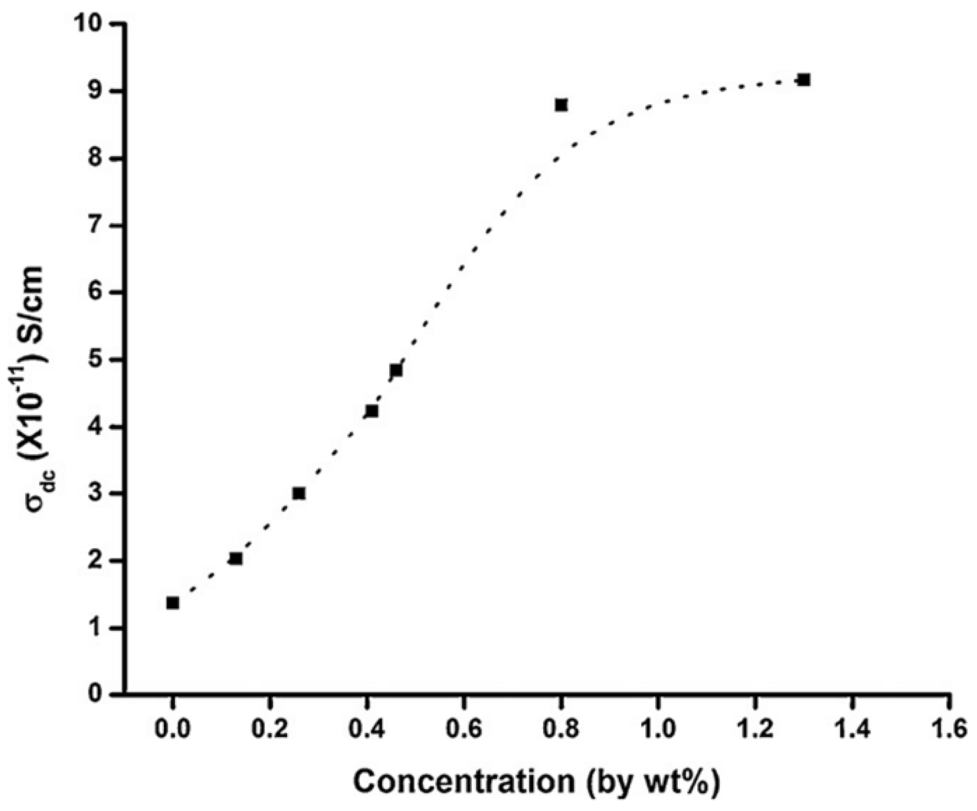
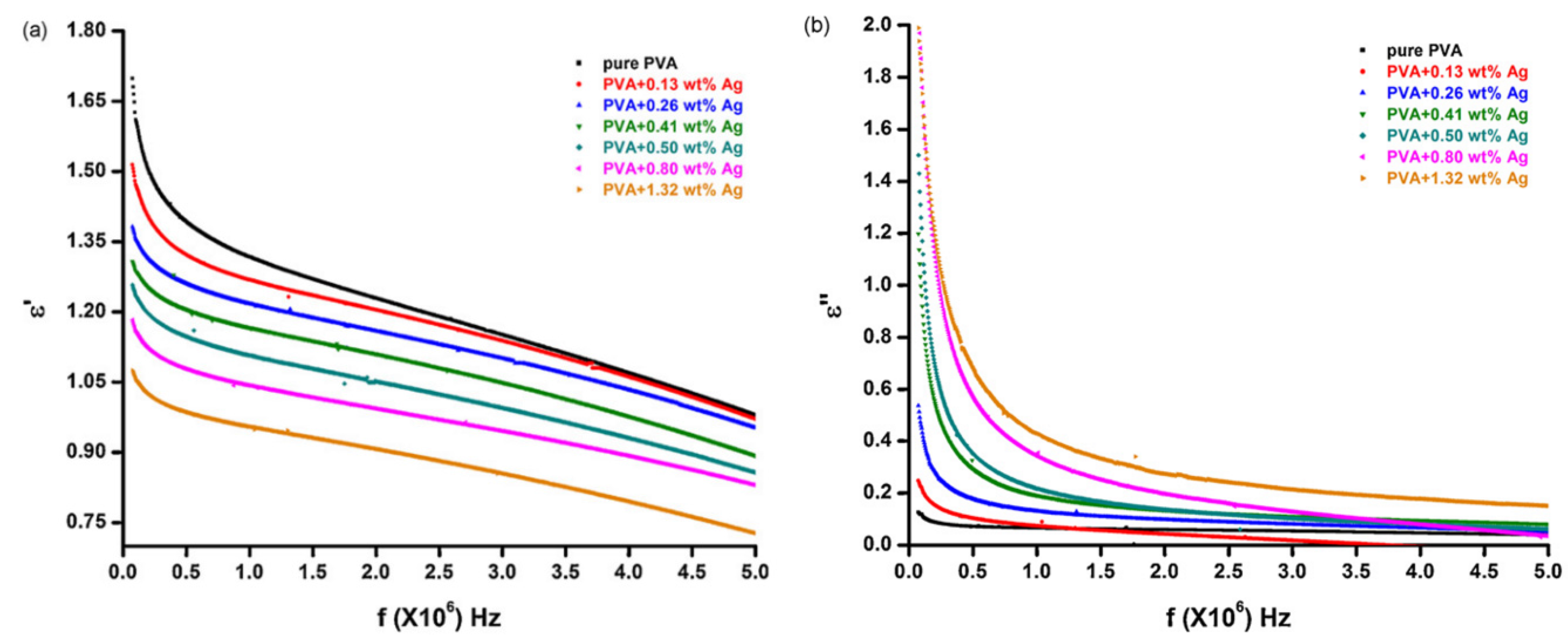
  98. Mahendia, S.; Tomara, A.K.; Kumara, S. Electrical conductivity and dielectric spectroscopic studies of PVA-Ag nanocomposite films. J. Alloy. Compd. 2010, 508, 406–411. [Google Scholar] [CrossRef]
  99. Bhajanti, R.F.; Ravindrachary, V.; Harisha, A.; Ranganathaiah, G.; Kumaraswamy, G.N. Effect of barium chloride doping on PVA microstructure: positron annihilation study. Appl. Phys. A 2007, 87, 797–805. [Google Scholar] [CrossRef]
  100. Devi, C.U.; Sharma, A.K.; Rao, V.V.R.N. Electrical and optical properties of pure and silver nitrate-doped polyvinyl alcohol films. Mater. Lett. 2002, 56, 167–174. [Google Scholar] [CrossRef]
  101. Reddy, C.V.S.; Han, X.; Zhu, Q.-Y.; Mai, L.-Q.; Chen, W. Dielectric spectroscopy studies on (PVP + PVA) polyblend film. Microelectron. Eng. 2006, 83, 281–285. [Google Scholar] [CrossRef]
  102. Campbell, J.A.; Goodwin, A.A.; Simon, G.P. Dielectric relaxation studies of miscible polycarbonate/polyester blends. Polymer 2001, 42, 4731–4741. [Google Scholar] [CrossRef]
  103. Abd El Mongy, S. Preparation and Spectroscopic Studies of Rhodamine 6G Doped Polystyrene. Aust. J. Basic Appl. Sci. 2009, 3, 1954–1963. [Google Scholar]
  104. Bhargav, P.B.; Sarada, B.A.; Sharma, A.K.; Rao, V.V.R.N. Electrical conduction and dielectric relaxation phenomena of PVA based polymer electrolyte films. J. Macromol. Sci. A Pure Appl. Chem. 2009, 47, 131–137. [Google Scholar] [CrossRef]
  105. Mardare, D.; Rusu, G.I. Comparison of the dielectric properties for doped and undoped TiO2 thin films. J. Optoelectron. Adv. Mater. 2004, 6, 333–336. [Google Scholar]
  106. Fuyuki, T.; Matsunmi, H. Electronic Properties of the interface between Si and TiO2 deposited at very low temperatures. Jpn. J. App. Phys. 1986, 25, 1288–1291. [Google Scholar] [CrossRef]
  107. Ramya, C.S.; Savutha, T.; Selvasekarapandian, S.; Hirankumar, G. Transport mechanism of Cu-ion conducting PVA based solid-polymer electrolyte. Ionics 2005, 11, 436–441. [Google Scholar] [CrossRef]
  108. Liu, Z.; Zhang, L.; Poyraz, S.; Zhang, X. Conducting polymer-metal nanocomposites synthesis and their sensory applications. Curr. Org. Chem. 2013, 17, 2256–2267. [Google Scholar] [CrossRef]
  109. Long, Y.Z.; Li, M.M.; Gu, C.; Wan, M.; Duvail, J.L.; Liu, Z.; Fan, Z. Recent advances in synthesis, physical properties and applications of conducting polymer nanotubes and nanofibers. Prog. Polym. Sci. 2011, 36, 1415–1442. [Google Scholar] [CrossRef]
  110. Xia, Y.N.; Yang, P.D.; Sun, Y.G.; Wu, Y.Y.; Mayers, B.; Gates, B.; Yin, Y.D.; Kim, F.; Yan, Y.Q. One-dimensional nanostructures: synthesis, characterization, and applications. Adv. Mater. 2003, 15, 353–389. [Google Scholar] [CrossRef]
  111. Tran, H.D.; Li, D.; Kaner, R.B. One-dimensional conducting polymer nanostructures: Bulk synthesis and applications. Adv. Mater. 2009, 21, 1487–1499. [Google Scholar] [CrossRef]
  112. Lu, X.F.; Zhang, W.J.; Wang, C.; Wen, T.C.; Wei, Y. One-dimensional conducting polymer nanocomposites: Synthesis, properties and applications. Prog. Polym. Sci. 2011, 36, 671–712. [Google Scholar] [CrossRef]
  113. Li, C.; Bai, H.; Shi, G.Q. Conducting polymer nanomaterials: electrosynthesis and applications. Chem. Soc. Re. 2009, 38, 2397–2409. [Google Scholar] [CrossRef] [PubMed]
  114. Ronkainen, N.J.; Halsall, H.B.; Heineman, W.R. Electrochemical biosensors. Chem. Soc. Rev. 2010, 39, 1747–1763. [Google Scholar] [CrossRef] [PubMed]
  115. Asefa, T.; Duncan, C.T.; Sharma, K.K. Recent advances in nanostructured chemosensors and biosensors. Analyst 2009, 134, 1980–1990. [Google Scholar] [CrossRef] [PubMed]
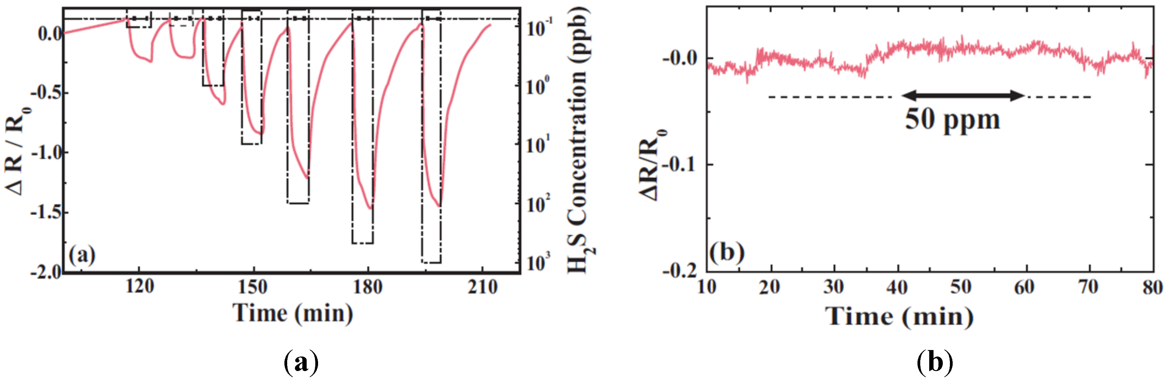
  116. Shirsat, M.D.; Bangar, M.A.; Deshusses, M.A.; Myung, N.V.; Mulchandani, A. Polyaniline nanowires-gold nanoparticles hybrid network based chemiresistive hydrogen sulfide sensor. Appl. Phys. Lett. 2009, 94. [Google Scholar] [CrossRef]
  117. Srivastava, S.; Kumar, S.; Vijay, Y.K. Preparation and characterization of tantalum/polyaniline composite based chemiresistor type sensor for hydrogen gas sensing application. Int. J. Hydrog. Energy 2012, 37, 3825–3832. [Google Scholar] [CrossRef]
  118. Li, X.; Gao, Y.; Gong, J.; Zhang, L.; Qu, L. Polyaniline/Ag composite nanotubes prepared through UV rays irradiation via fiber template approach and their NH3 gas sensitivity. J. Phys. Chem. C 2009, 113, 69–73. [Google Scholar] [CrossRef]
  119. Yang, X.M.; Li, L.; Yan, F. Polypyrrole/silver composite nanotubes for gas sensors. Sens. Actuat. B Chem. 2010, 145, 495–500. [Google Scholar] [CrossRef]
  120. Park, E.; Kwon, O.S.; Park, S.J.; Lee, J.S.; You, S.; Jang, J.J. One-pot synthesis of silver nanoparticles decorated poly(3,4-ethylenedioxythiophene) nanotubes for chemical sensor application. J. Mater. Chem. 2012, 22, 1521–1526. [Google Scholar] [CrossRef]
  121. Peng, C.; Zhang, S.; Jewell, D.; Chen, G.Z. Carbon nanotube and conducting polymer composites for supercapacitors. Prog. Nat. Sci. 2008, 18, 777–788. [Google Scholar] [CrossRef]
  122. Xiao, R.; Cho, S., II; Liu, R.; Lee, S.B. Controlled electrochemical synthesis of conductive polymer nanotube structures. J. Am. Chem. Soc. 2007, 129, 4483–4489. [Google Scholar] [CrossRef] [PubMed]
  123. Li, D.; Huang, J.; Kaner, R.B. Polyaniline nanofibers: a unique polymer nanostructurefor versatile applications. Acc. Chem. Res. 2009, 42, 135–145. [Google Scholar] [CrossRef] [PubMed]
  124. Köhler, J.M.; Kraus, I.; Faerber, J.; Serra, C. Continuous-flow preparation of nanoporous metal/polymer composite particles by in situ synthesis of silver nanoparticles in photopolymerized acrylate/diethylene glycol droplets. J. Mater. Sci. 2013, 48, 2158–2166. [Google Scholar] [CrossRef]
  125. Detsi, E.; Onck, P.R.; de Hosson, J.T.M. Electrochromic artificial muscles based on nanoporous metal-polymer composites. Appl. Phys. Lett. 2013, 103. [Google Scholar] [CrossRef]
  126. Meenach, S.A.; Burdick, J.; Kunwar, A.; Wang, J. Metal/conducting-polymer composite nanowires. Small 2007, 3, 239–243. [Google Scholar] [CrossRef] [PubMed]
  127. Wang, K.; Weissmüller, J. Composites of nanoporous gold and polymer. Adv. Mater. 2013, 25, 1280–1284. [Google Scholar] [CrossRef] [PubMed]
  128. Bian, X.; Lu, X.; Jin, E.; Kong, L.; Zhang, W.; Wang, C. Fabrication of Pt/polypyrrole hybrid hollow microspheres and their application in electrochemical biosensing towards hydrogen peroxide. Talanta 2010, 81, 813–818. [Google Scholar] [CrossRef] [PubMed]
  129. Hung, C.C.; Wen, T.-C.; Wei, Y. Site-selective deposition of ultra-fine Au nanoparticles on polyaniline nanofibers for H2O2 sensing. Mater. Chem. Phys. 2010, 122, 392–396. [Google Scholar] [CrossRef]
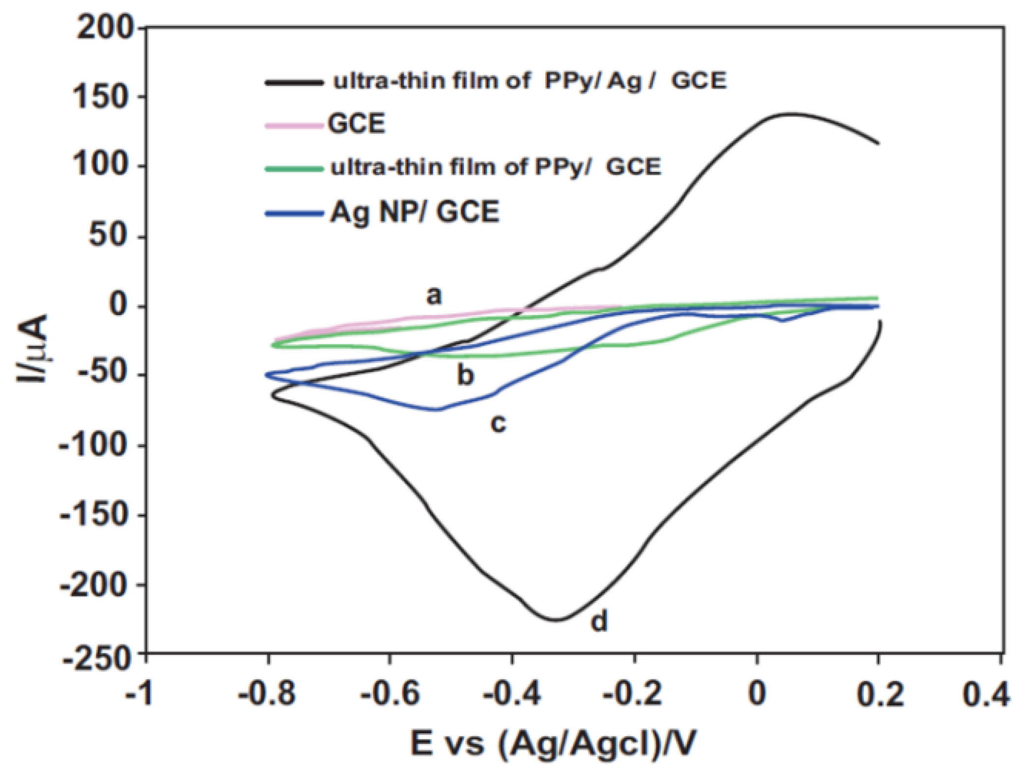
  130. Mahmoudian, M.R.; Alias, Y.; Basirun, W.J.; Ebadi, M. Preparation of ultrathin polypyrrole nanosheets decorated with Ag nanoparticles and their application in hydrogen peroxide detection. Electrochim. Acta 2012, 72, 46–53. [Google Scholar] [CrossRef]
  131. Qin, X.; Luo, W.Y.; Chang, G.; Sun, X. Preparation of Ag nanoparticle decorated polypyrrole colloids and their application for H2O2 detection. Electrochem. Commun. 2011, 13, 785–787. [Google Scholar] [CrossRef]
  132. Guo, S.; Dong, S.; Wang, E. Polyaniline/Pt hybrid nanofibers: High efficiency nanoelectrocatalysts for electrochemical devices. Small 2009, 16, 1869–1876. [Google Scholar] [CrossRef] [PubMed]
  133. Li, X.; Xie, H.; Li, Y. Fabrication of gold nanoparticles/polypyrrole composite-modified electrode for sensitive hydroxylamine sensor design. J. Solid State Electrochem. 2012, 16, 795–802. [Google Scholar] [CrossRef]
  134. Liu, Z.; Liu, Y.; Zhang, L.; Poyraz, S.; Lu, N.; Kim, M.; Smith, J.; Wang, X.; Yu, Y.; Zhang, X. Controlled synthesis of transition metal/conducting polymer nanocomposites. Nanotechnology 2012, 23. [Google Scholar] [CrossRef] [PubMed]
  135. Xia, L.; Wei, Z.; Wan, M. Conducting polymer nanostructures and their application in biosensors. J. Colloid Interface Sci. 2010, 341, 1–11. [Google Scholar] [CrossRef] [PubMed]
  136. Yogeswaran, U.; Chen, S.M. A review on the electrochemical sensors and biosensors composed of nanowires as sensing material. Sensors 2008, 8, 290–313. [Google Scholar] [CrossRef]
  137. Crespilho, F.N.; Iost, R.M.; Travain, S.A., Jr.; Oliveira, O.N.; Zucolotto, V. Enzyme immobilization on Ag nanoparticles/polyaniline nanocomposites. Biosens. Bioelectron. 2009, 24, 3073–3077. [Google Scholar] [CrossRef] [PubMed]
  138. Atta, N.F.; El-Kady, M.F. Novel poly(3-methylthiophene)/Pd, Pt nanoparticle sensor: Synthesis, characterization and its application to the simultaneous analysis of dopamine and ascorbic acid in biological fluids. Sens. Actuat. B Chem. 2010, 145, 299–310. [Google Scholar] [CrossRef]
  139. Brabec, C.J.; Gowrisanker, S.; Halls, J.J.M.; Laird, D.; Jia, S.; Williams, S.P. Polymer-fullerene bulk-heterojunction solar cells. Adv. Mater. 2010, 22, 3839–3856. [Google Scholar] [CrossRef] [PubMed]
  140. Lobez, J.M.; Andrew, T.L.; Bulovic, V.; Swager, T.M. Improving the performance of P3HT-fullerene solar cells with side-chain-functionalized poly(thiophene) additives: A new paradigm for polymer design. ACS Nano 2012, 6, 3044–3056. [Google Scholar] [CrossRef] [PubMed]
  141. Kim, Y.H.; Sachse, C.; Machala, M.L.; May, C.; Muller-Meskamp, L.; Leo, K. Highly conductive pedot:pss electrode with optimized solvent and thermal post-treatment for ITO-free organic solar cells. Adv. Funct. Mater. 2011, 21, 1076–1081. [Google Scholar] [CrossRef]
  142. Feng, T.; Xie, D.; Lin, Y.; Zhao, H.; Chen, Y.; Tian, H.; Ren, T.; Li, X.; Li, Z.; Wang, K.; Wu, D.; Zhu, H. Efficiency enhancement of graphene/silicon-pillar-array solar cells by HNO3 and PEDOT-PSS. Nanoscale. 2012, 4, 2130–2133. [Google Scholar] [CrossRef] [PubMed]
  143. Jeong, S.; Garnett, E.C.; Wang, S.; Yu, Z.; Fan, S.; Brongersma, M.L.; McGehee, M.D.; Cui, Y. Hybrid silicon nanocone-polymer solar cells. Nano Lett. 2012, 12, 2971–2976. [Google Scholar] [CrossRef] [PubMed]
  144. Shen, X.J.; Sun, B.Q.; Liu, D.; Lee, S.T. Hybrid heterojunction solar cell based on organic-inorganic silicon nanowire array architecture. J. Am. Chem. Soc. 2011, 133, 19408–19415. [Google Scholar] [CrossRef] [PubMed]
  145. Wu, J.L.; Chen, F.C.; Hsiao, Y.S.; Chien, F.C.; Chen, P.; Kuo, C.H.; Huang, M.H.; Hsu, C.S. Surface plasmonic effects of metallic nanoparticles on the performance of polymer bulk heterojunction solar cells. ACS Nano 2011, 5, 959–967. [Google Scholar] [CrossRef] [PubMed]
  146. Kirkeminde, A.; Retsch, M.; Wang, Q.; Xu, G.; Hui, R.; Wu, J.; Ren, S. Surface-passivated plasmonic nano-pyramids for bulk heterojunction solar cell photocurrent enhancement. Nanoscale 2012, 4, 4421–4425. [Google Scholar] [CrossRef] [PubMed]
  147. Choi, H.; Chen, W.T.; Kamat, P.V. Know thy nano neighbor. Plasmonic versus electron charging effects of metal nanoparticles in dye-sensitized solar cells. ACS Nano 2012, 6, 4418–4427. [Google Scholar] [CrossRef] [PubMed]
  148. Atwater, H.A.; Polman, A. Plasmonics for improved photovoltaic devices. Nat. Mater. 2010, 9, 205–213. [Google Scholar] [CrossRef] [PubMed]
  149. Schaadt, D.M.; Feng, B.; Yu, E.T. Enhanced semiconductor optical absorption via surface plasmon excitation in metal nanoparticles. Appl. Phys. Lett. 2005, 86. [Google Scholar] [CrossRef]
  150. Chen, X.; Jia, B.; Saha, J.K.; Cai, B.; Stokes, N.; Qiao, Q.; Wang, Y.; Shi, Z.; Gu, M. Broadband enhancement in thin-film amorphous silicon solar cells enabled by nucleated silver nanoparticles. Nano Lett. 2012, 12, 2187–2192. [Google Scholar] [CrossRef] [PubMed]
  151. Pillai, S.; Catchpole, K.R.; Trupke, T.; Green, M.A. Surface plasmon enhanced silicon solar cells. J. Appl. Phys. 2007, 101. [Google Scholar] [CrossRef]
  152. Diukman, I.; Orenstein, M. How front side plasmonic nanostructures enhance solar cell efficiency. Sol. Energy Mater. Sol. Cells 2011, 95, 2628–2631. [Google Scholar] [CrossRef]
  153. Chen, F.C.; Wu, J.L.; Lee, C.L.; Hong, Y.; Kuo, C.H.; Huang, M.H. Plasmonic-enhanced polymer photovoltaic devices incorporating solution-processable metal nanoparticles. Appl. Phys. Lett. 2009, 95. [Google Scholar] [CrossRef]
  154. Pei, J.; Tao, J.; Zhou, Y.; Dong, Q.; Liu, Z.; Li, Z.; Chen, F.; Zhang, J.; Xu, W.; Tian, W. Efficiency enhancement of polymer solar cells by incorporating a self-assembled layer of silver nanodisks. Sol. Energy Mater. Sol. Cells 2011, 95, 3281–3286. [Google Scholar] [CrossRef]
  155. Tang, Z.; Liu, Q.; Chen, Q.; Khatri, I.; Shirai, H. Plasmonic-enhanced crystalline silicon/organic heterojunction cells by incorporating gold nanoparticles. Phys. Status Solidi A 2014, 211, 1179–1183. [Google Scholar] [CrossRef]
  156. Heness, G. Metal-polymer nanocomposites. In Advances in Polymer Nanocomposites: Types and Application; Gao, F., Ed.; Woodhead Publishing: Sawston, UK, 2012. [Google Scholar]
  157. Bockstaller, M.R.; Mickiewicz, R.A.; Thomas, E.L. Block copolymer nanocomposites: Perspectives for tailored functional materials. Adv. Mate. 2005, 17, 1331–1349. [Google Scholar] [CrossRef]
  158. Dallas, P.; Sharma, V.K.; Zboril, R. Silver polymeric nanocomposites as advanced antimicrobial agents: Classifications, synthetic paths, applications, and perspectives. Adv. Colloid Interface Sci. 2011, 166, 119–135. [Google Scholar] [CrossRef] [PubMed]
  159. Du, Y.; Shen, S.Z.; Cai, K.; Casey, P.S. Research progress on polymer-inorganic thermoelectric nanocomposite materials. Prog. Polym. Sci. 2012, 37, 820–841. [Google Scholar] [CrossRef]
  160. Kumar, A.P.; Depan, D.; Tomer, N.S.; Singh, R.P. Nanoscale particles, for polymer degradation and stabilization-trends and future perspectives. Prog. Polym. Sci. 2009, 34, 479–515. [Google Scholar] [CrossRef]

