Improved Performance of Perovskite Light-Emitting Diodes by Quantum Confinement Effect in Perovskite Nanocrystals


1
Department of Electro-optical Engineering, National Taipei University of Technology, 1, 3 Section, Chung-Hsiao East Road, Taipei 106, Taiwan
2
Department of Optics and Photonics, National Central University, 300 Chung-Da Rd., Chung-Li 32001, Taiwan
*
Authors to whom correspondence should be addressed.
Nanomaterials 2018, 8(7), 459; https://doi.org/10.3390/nano8070459
Submission received: 25 May 2018
/
Revised: 15 June 2018
/
Accepted: 19 June 2018
/
Published: 25 June 2018
(This article belongs to the Special Issue Optoelectronic Nanodevices)
Abstract
:In this study, we demonstrate an easy and reliable solution-processed technique using an extra adductive in the perovskite precursor solution. Using this method, a dense and uniform morphology with full surface coverage and highly fluorescent films with nanoscale crystal grains can be obtained. The high exciton binding energy in the resulting films employing octylammonium bromide (OAB) adductives proved that high fluorescence originated from the quantum confinement effect. The corresponding perovskite light-emitting diodes (PeLEDs) that were based on this technique also exhibited excellent device performance.
1. Introduction
Since the report on the perovskite light-emitting diodes (PeLEDs) in 2012 [1] expanded the research range of lead halide perovskites from their photovoltaic applications, a series of studies on device structures and deposition methods [2,3,4,5,6,7,8,9,10] have been presented. As a result, excellent electroluminescence efficiency of 42.9 cd/A has been achieved by employing an additive-based nanocrystal pinning technique [11].
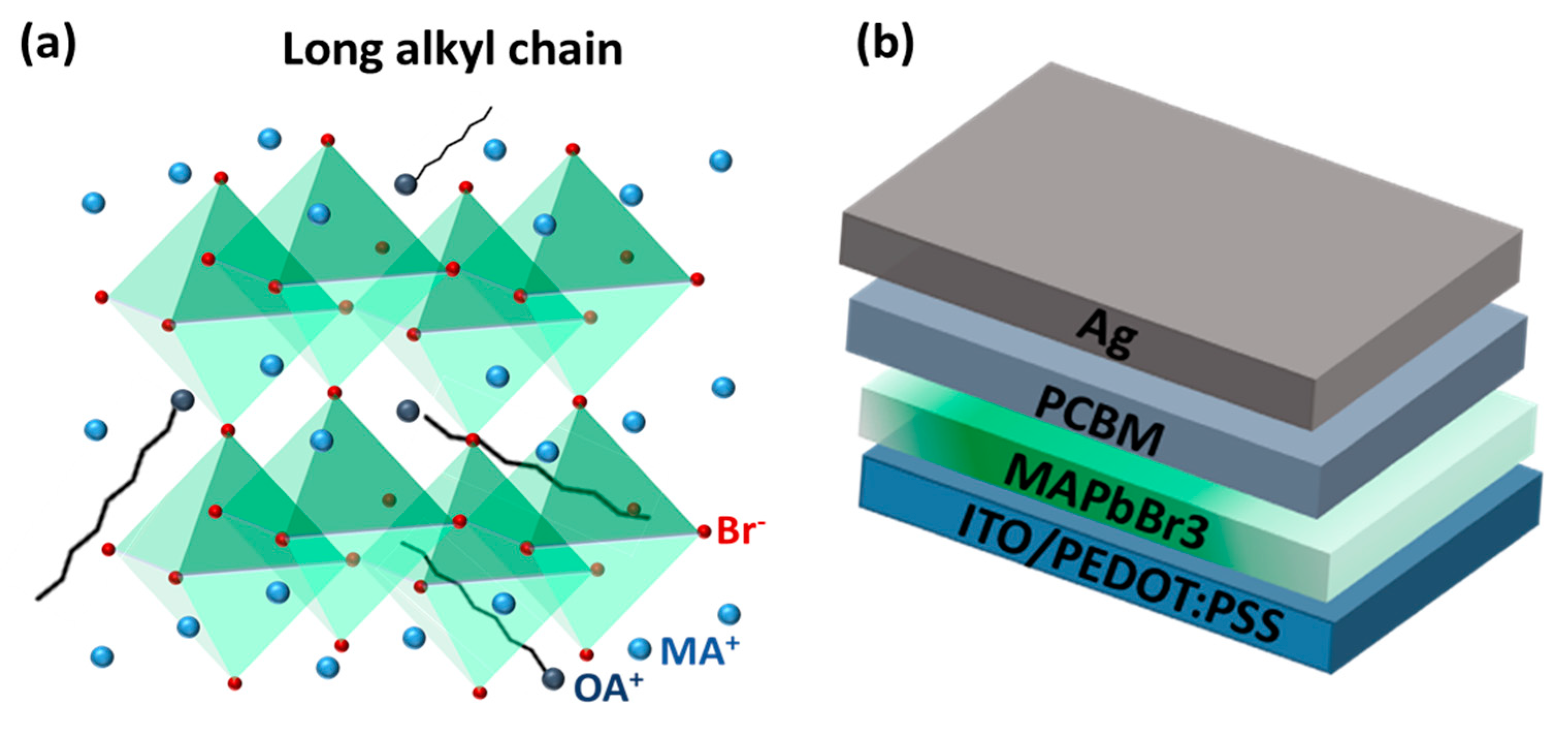
The active layer of PeLEDs and CH3NH3PbBr3 (MAPbBr3) can be prepared by using a simple solution-processed coating, where a precursor solution containing CH3NH3Br (MAB) and PbBr2 is spin-coated on the substrates and washed using toluene to rapidly crystalize while spinning [12,13]. The resulting film exhibited better optoelectronic properties, such as high mobility [14,15,16,17], long and balanced electron-hole diffusion lengths [18,19], low bulk defect densities, and slow Auger recombination [20] compared to the previous solution-processed semiconductors. On the other hand, Pérez-Prieto et al. [21,22] first reported that MAPbBr3 perovskite quantum dots (QDs) were achievable and they synthesized them using octylammonium bromide (CH3(CH2)7NH3Br; OAB) with a long alkyl chain as a capping ligand to stabilize them. The longer alkyl chain cations are embedded in the MAPbBr3 lattice to replace the methyl ammonium cations and their long chains dangling outside the lattice, as illustrated in Figure 1a. Because of the repulsion forces between long alkyl chains, the growth of the perovskite array is suppressed in three dimensions, resulting in perovskite QDs being produced. Although it is well known that colloidal QD dispersions exhibit narrow-band emission and high photoluminescence (PL) efficiency [21,22,23,24,25,26,27], the uniform, smooth, and large-area films are difficult to prepare by directly using colloidal dispersions. In addition, some solution-processed methods for highly efficient PeLEDs with high-quality perovskite films, such as the additive-based nanocrystal pinning technique, require great skill for processing controls. Therefore, it is necessary to develop an easy and reliable method for obtaining high-quality perovskite films with nanoscale crystal grains for high-performance PeLEDs [28,29,30].
In this study, we demonstrate the preparation of MAPbBr3 thin films with highly uniform and dense nanoscale grains through a simple spin-coating method using OAB as an additive (Figure 1a). Highly fluorescent thin films with full-surface coverage were achieved by optimizing the amount of OAB in the perovskite precursors. Highly efficient PeLEDs were also prepared using the resulting MAPbBr3 thin films as active layers. The champion device based on the OAB adductive method exhibited a maximum luminance of 310 cd/m2 (at 4.5 V) and a maximum luminous current efficiency of 1.21 cd/A (at 4.5 V). We further show that the improved performance of PeLEDs and the enhanced fluorescence of MAPbBr3 thin films are due to high exciton binding energy in nanometer-sized crystal grains, which leads to reduced nonradiative recombination and increased emission efficiency.
2. Materials and Methods
PeLEDs with a device structure of glass/indium tin oxide (ITO)/poly(3,4-ethylenedioxythiophene) polystyrene sulfonate (PEDOT:PSS)/MAPbBr3/[6,6]-phenyl-C61-butyric acid methyl ester (PCBM)/Ag were used in this study, as illustrated in Figure 1b. The PEDOT:PSS layers using AI-4083 (Heraeus Clevios) were spin-coated on a cleaned ITO substrate at 5000 rpm for 30 s and were post-annealed at 120 °C for 10 min. PbBr2 (99.999%; Sigma-Aldrich, St. Louis, MO, USA), methylammonium iodide (MAB; Lumtec, Hsinchu, Taiwan), and octylammonium bromide (OAB; Lumtec, Hsinchu, Taiwan) were dissolved in a dimethyl sulfoxide (DMSO)/dimethylformamide (DMF) mixture (7:3, v/v) as the precursor, with an MAPbBr3 concentration of 0.5 M. Different OAB ratios were prepared with the weight ratio of MAB:OAB. The perovskite precursors were then spin-coated onto the PEDOT:PSS layers at 5000 rpm for 30 s, with 2 mL of anhydrous toluene dropped at 27 s during spin-coating. The large amount of toluene ensured the removal of OAB due to the long alkyl chain approaching nonpolar character. The as-deposited films were post-annealed at 90 °C for 5 min, and after being cooled to room temperature, [6,6]-phenyl-C61-butyric acid methyl ester (PCBM) dissolved in chlorobenzene (20 mg/mL) was then spin-coated on them at 1200 rpm for 30 s. Ag electrodes (100 nm) were evaporated through a metal mask to define the device area (0.1 cm2).
The crystalline microstructure, absorbance spectra, and surface morphology of the films were determined by X-ray diffraction with Cu-Kα radiation (D8 Discover, Bruker, Karlsruhe, Germany), UV-visible spectroscopy (U-4100, Hitachi High-Technologies Co., Tokyo, Japan), and a field-emission scanning electron microscope (GeminiSEM, Zeiss, Oberkochen, Germany), respectively. The photoluminescence (PL) spectra were measured using an optical microscope-based system (UniRAM, Protrustech, New Taipei, Taiwan) with an excitation of 405 nm. The temperature-dependent photoluminescence (PL) spectra was measured under a nitrogen-filled atmosphere. The current density-voltage-luminesce (J-V-L) characteristics were measured using a Keithley 2400 combined with a SpectraScan Spectroradiometer (PR-670, Photo Research, New York, NY, USA).
3. Results and Discussion
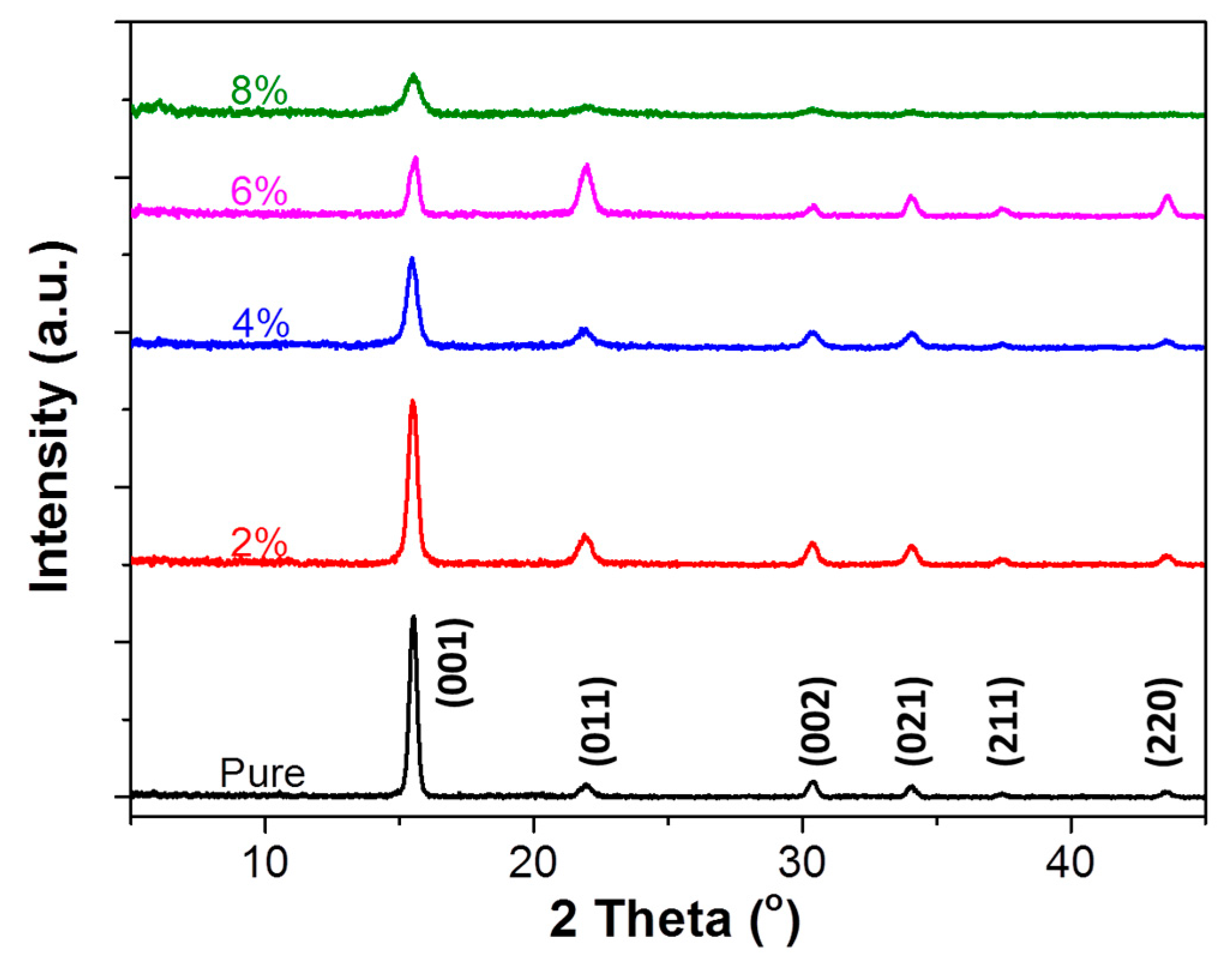
To understand how the ratio of OAB to MAPbBr3 in the precursor solution affects the performance of the resulting perovskite light-emitting diodes, X-ray diffraction patterns of MAPbBr3 films grown with different OAB ratios were collected, and these are shown in Figure 2 (the corresponding 2D-XRD is shown in Supplementary Figure S1). Pure MAPbBr3 cubic phase with (001), (011), (002), (021), (211), and (220) at 2θ range from 5–45° were identified [23] in all diffractograms. The thicknesses of the MAPbBr3 films that were obtained by α-step had no significant differences at different OAB ratios (~200 nm; Supplementary Figure S2). Using a higher OAB ratio, the intensity of the (001) peak decreased and full width at half maximum (FWHM) increased, implying a smaller MAPbBr3 grain size. Also, when the OAB ratio was increased to 6%, the intensity and FWHM ratio of the (001) to (110) peak decreased. Reduced crystallinity of MAPbBr3 with an OAB adductive compared to pure MAPbBr3 films suggests that the long alkyl chain of OAB indeed acts as a better capping ligand to limit MAPbBr3 grain growth. Therefore, the OAB ratio in the precursor solution was confirmed to suppress the grain growth in the MAPbBr3 films. Interestingly, when applying a higher OAB ratio (8%), MAPbBr3 became very weak and produced a new diffraction peak at a low angle (~6°). Most reported XRD patterns for MAPbBr3 were only detected from 10° (2θ > 10°), therefore it was difficult to know the exact components and structures of this new phase by only depending on XRD. Nevertheless, according to the Scherrer equation [30], we can obtain that the low-angle peak corresponded to a larger lateral ordered spacing.
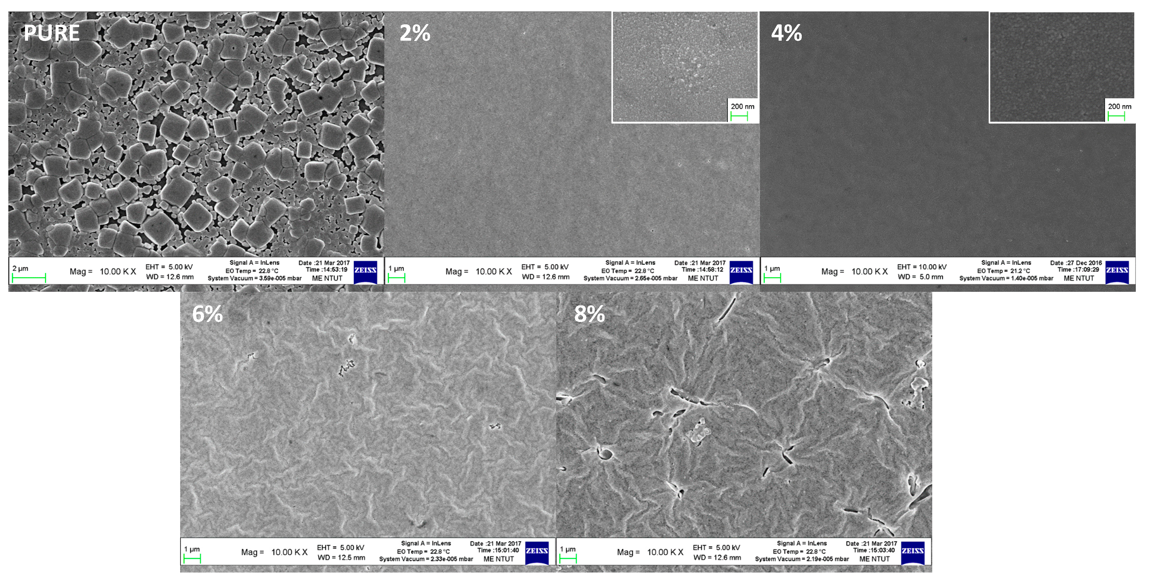
Furthermore, the OAB ratio also affected the surface morphology of the MAPbBr3 films, as revealed by scanning electron microscopy (SEM) micrographs, shown in Figure 3. The morphology of the pure MAPbBr3 films showed large and nonuniform cubic grains from 200 to 1000 nm, but some interspace existed between the micrograins, which may have increased leakage due to the direct contact between the upper and bottom layers without passing through the perovskite films. The unwanted broad size distribution was due to the rapid crystallization process in the perovskite thin films [31,32], leading to not enough time for the thermodynamically spontaneous process, i.e., the well-known Ostwald ripening process [33,34], to form small-size crystals that recrystallized to large grains. Several methods have been suggested to improve this phenomenon in perovskite thin films, such as the solvent-annealing process [35], mixed halide treatment [34], and HBr/DMF cosolvent [10]. Applying OAB as an additive, the grain size was significantly reduced, which was in accord with XRD results. Smooth, uniform, and dense perovskite films (grain size of about 20 nm) were observed when the OAB ratio was equal to 2% and 4%, and furthermore, the grain size of the 2% sample was more uniform than that of the 4% sample (see insets in Figure 3). This suggested that the OAB additive is the main factor in the formation of nanograins in perovskite film. This dense MAPbBr3 film was also reported using the HBr/DMF cosolvent method [10], which originated from slow crystallization rates during deposition. Unlike those, the reason in our case for morphological control was the grain growth being limited by the long alkyl chain of OAB. Therefore, our grain sizes were much smaller than theirs and were much like those using an additive-based nanocrystal pinning technique [11]. Under a higher OAB ratio, inhomogeneous humped structures could be seen, resulting in rough films with some cracks and defects, which negatively affected the device performance. The humped structure may be attributed to large-size ordered packing that was formed from the grain aggregation. This may be why the low angle phase was found in the XRD pattern. These results indicate that the film morphology of MAPbBr3 films is strongly influenced by the OAB ratio in the precursor solution. This easy method, using an OAB adductive, provides a general way to control the morphology and the surface coverage of MAPbBr3 films.
Figure 4a shows the PL spectra of samples with different OAB ratios in the precursor solution. The intensity increased using lower OAB ratios (2% and 4%), but decreased using low OAB ratios (6% and 8%). The PL intensity in the 4% sample is better than that in the 2% sample, which can be attributed to more homogeneous grain size (Figure 3). The weak PL in the 6 and 8% samples may be due to the poor crystallinity and grain aggregation, which may increase the dissociation rate. However, the PL intensity in thin films compared to that in dispersions is much more complicated [36,37] due to exciton dissociation between grains or bottom/upper layers, leading to radiative loss. Therefore, the smaller grains in the 2% and 4% films had more grain boundaries (more grain package) to provide PL quenching sites, but the 2% and 4% samples exhibited better PL intensities. The reason is that excitons are confined in the nanometer-sized grains [21,22], leading to strong PL emission. These results are similar to those using colloidal perovskite QD dispersions to directly deposit thin films [38,39,40,41]. An exciton diffusion length of 67 nm in MAPbBr3 films with nanograins was reported, which is much smaller than that of solution-processed perovskite films [11]. Moreover, a significant blue shift can be observed in PL spectra, in that emission wavelength decreased with an increase in the OAB ratio, from 540.1 nm (pure film) to 531.7 nm (8%). Similarly, the absorption edges in ultraviolet-visible (UV-vis) spectra (Figure 3b) also showed the same trend. The fitting bandgap (the corresponding Tauc plots shown in Supplementary Figure S3) from UV-vis spectra increased with an increase in the OAB ratio. The blue shift can typically be attributed to the quantum confinement effect in the nanocrystal [21,22]. Besides, nanocrystal materials have sharper density of states than higher dimensional materials. Therefore, they permit more electrons to occupy the states in conduction band, such that opportunity of spontaneous emission increases.
Figure 5a shows the current–density vs. voltage (J-V) curves for PeLEDs using different OAB ratios. All of the curves revealed diode behavior. The inserted image in Figure 5a shows that our PeLED displayed a text patterned by a metal mask for Ag evaporation. Figure 5b,c shows the luminance vs. voltage (L-V) and the current efficiency vs. voltage (CE-V) of our PeLEDs with different OAB ratios. The optimized PeLED that was prepared with the OAB ratio of 6% exhibited a maximum luminance of 310 cd/m2 (at 4.5 V) and a maximum luminous current efficiency of 1.21 cd/A (at 4.5 V). The PeLED that was based on the pure MAPbBr3 film without OAB adductives showed poor luminance characteristics (maximum CE = 0.32 cd/A), mainly due to high leakage current, as mentioned in Figure 3, that was induced from the lateral space between the MAPbBr3 grains or the pinholes on the film surface. Maximum current efficiency was achieved (1.21 cd/A) when the OAB ratio was increased to 4%. The excellent performance at the OAB ratio of 4% was mainly due to the dense and uniform MAPbBr3 layer with full coverage avoiding leakage, the smooth surface providing good contact with the electrode transporting layer (PCBM), and the MAPbBr3 nanograins having an enhanced radiative recombination rate for injected carriers. In contrast, poor device performance at higher OAB ratios (6% and 8%) may have been from the grain aggregation, leading to an increased dissociation path and a rough film surface. Furthermore, the electroluminescence (EL) spectra also exhibited a blue shift (Figure 5d), which was consistent with the PL observation. It is worth mentioning that the maximum luminance and current efficiency values of our PeLED are comparable to those of the previously reported PeLEDs based on MAPbBr3 active layers [2,3,4,5,6,7,8,9,10]. Figure 5e shows the energy band structure to explain the mechanism of the radiative recombination caused by the quantum confinement effect, as results of the blue shift and enhance the spontaneous emission of the electroluminescence (EL) spectra. In Figure 5, the phenomenon of luminance decay at high applied voltage is caused either by heat due to the series resistance of the devices or by damage due to the high electrical field.
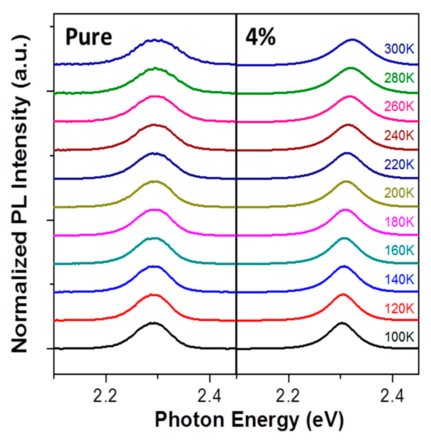
To better realize the nature of strong PL emission in the MAPbBr3 nanograins formed by the OAB adductive, the excitonic characteristics of the MAPbBr3 films should be considered. As we reported previously [42], temperature-dependent photoluminescence (TDPL) can be used to determine the exciton binding energy by linear fitting with a PL spectral broadening equation [43] at different temperatures:
where hΔν is the full width at half maximum (FWHM) of the PL spectrum at some temperature, hΔν0 is the FWHM of the PL spectrum at the initial temperature, hνT is related to the thermal dissociation rate, Eb is the exciton binding energy, KB is the Boltzmann constant, and T is the temperature. The PL spectra at temperatures from 100 to 300 K for the MAPbBr3 films deposited with (4%) and without (pure) the OAB adductive are shown in Figure 6. The peak of both samples significantly broadened with increased temperature due to exciton–phonon interaction [17]. Grätzel et al. suggested that the dual PL emissions in MAPbBr3 at temperatures below 175 K were due to the coexistence of MA-ordered and MA-disordered domains in the MAPbBr3 array [44]. However, only one peak of both samples can be found in Figure 6. Indeed, in our case, linear fitting could not be estimated (very low R-square) if the temperature selected was from 100 to 300 K. Therefore, the temperature was set from 180 to 300 K for linear fitting in Supplementary Figure S4. R-square over 0.99 reveals a good fit, and exciton binding energies of 48 and 85 meV were determined for pure MAPbBr3 film and film using the OAB adductive, respectively. The higher exciton binding energy of the MAPbBr3 film with OAB compared to that of the pure MAPbBr3 film indicates strong exciton localization, which can block the exciton dissociation and increase the radiative recombination rate. Therefore, this provides evidence for the quantum confinement effect in nanometer-sized grains of MAPbBr3 film using the OAB adductive.
ln(hΔν − hΔν0) = ln(hνT) − Eb/KBT
4. Conclusions
In conclusion, we have demonstrated that the preparation method employing OAB adductive can obtain high-quality MAPbBr3 thin films. The addition of a small amount of OAB in the MAPbBr3 precursor solvent produces a dense and uniform film morphology with full surface coverage. Also, it enables the formation of nanoscale MAPbBr3 grains, which enhance PL emission due to the quantum confinement effect. The high exciton binding energy in the MAPbBr3 films that are formed by the OAB adductive is evidence for the quantum confinement effect in the nanometer-sized grains, which reduces exciton dissociation and enhances exciton radiation. The quantum confinement effect also affects bandgap, which shifts to a short wavelength with an increasing OAB ratio. A blue shift is found in absorbance, PL, and EL spectra at different OAB ratios. The optimized PeLED with an OAB ratio of 4% exhibited a maximum luminance of 310 cd/m2 (at 4.5 V) and a maximum luminous current efficiency of 1.21 cd/A (at 4.5 V). This study offers a promising approach for reliably depositing high-quality MAPbBr3 thin films for application to efficient PeLEDs.
Supplementary Materials
The following are available online at https://www.mdpi.com/2079-4991/8/7/459/s1, Figure S1: Original 2D XRD data of perovskite films with different OAB ratios, Figure S2: Film thicknesses of perovskite films with different OAB ratios. The error bars are standard deviations obtained from five samples, Figure S3: The corresponding Tauc plots from UV-vis spectra for linear fitting to determine bandgaps of perovskite films with different OAB ratios. The solid lines are fittings, Figure S4: Temperature-dependent data for linear fitting exciton binding energy. The solid lines are fittings.
Author Contributions
L.-C.C. wrote the paper, designed the experiments, and analyzed the data. Z.-L.T., D.-W.L., and Y.-S.L. prepared the samples and performed all of the measurements. S.-H.C. designed the experiments and discussed the results. All authors read and approved the final manuscript.
Funding
Financial support for this paper was provided by the Ministry of Science and Technology of the Republic of China under contract no. MOST 106-2221-E-027-091.
Acknowledgments
The authors want to thank Yu-Tai Tao, Institute of Chemistry, Academia Sinica, Taiwan, for his supportive chemistry knowledge and for providing J-V-L measurements. Financial support for this paper was provided by the Ministry of Science and Technology of the Republic of China under contract no. MOST 106-2221-E-027-091.
Conflicts of Interest
The authors declare no conflict of interest.
References
- Tan, Z.-K.; Moghaddam, R.S.; Lai, M.L.; Docampo, P.; Higler, R.; Deschler, F.; Price, M.; Sadhanala, A.; Pazos, L.M.; Credgington, D.; et al. Bright light-emitting diodes based on organometal halide perovskite. Nat. Nano 2014, 9, 687–692. [Google Scholar] [CrossRef] [PubMed]
- Kim, Y.-H.; Cho, H.; Heo, J.H.; Kim, T.-S.; Myoung, N.S.; Lee, C.-L.; Im, S.H.; Lee, T.-W. Multicolored Organic/Inorganic Hybrid Perovskite Light-Emitting Diodes. Adv. Mater. 2015, 27, 1248–1254. [Google Scholar] [CrossRef] [PubMed]
- Hoye, R.L.Z.; Chua, M.R.; Musselman, K.P.; Li, G.; Lai, M.-L.; Tan, Z.-K.; Greenham, N.C.; MacManus-Driscoll, J.L.; Friend, R.H.; Credgington, D. Enhanced Performance in Fluorene-Free Organometal Halide Perovskite Light-Emitting Diodes using Tunable, Low Electron Affinity Oxide Electron Injectors. Adv. Mater. 2015, 27, 1414–1419. [Google Scholar] [CrossRef] [PubMed] [Green Version]
- Li, G.; Tan, Z.-K.; Di, D.; Lai, M.L.; Jiang, L.; Lim, J.H.-W.; Friend, R.H.; Greenham, N.C. Efficient Light-Emitting Diodes Based on Nanocrystalline Perovskite in a Dielectric Polymer Matrix. Nano Lett. 2015, 15, 2640–2644. [Google Scholar] [CrossRef] [PubMed]
- Jaramillo-Quintero, O.A.; Sanchez, R.S.; Rincon, M.; Mora-Sero, I. Bright Visible-Infrared Light Emitting Diodes Based on Hybrid Halide Perovskite with Spiro-OMeTAD as a Hole-Injecting Layer. J. Phys. Chem. Lett. 2015, 6, 1883–1890. [Google Scholar] [CrossRef] [PubMed] [Green Version]
- Wong, A.B.; Lai, M.; Eaton, S.W.; Yu, Y.; Lin, E.; Dou, L.; Fu, A.; Yang, P. Growth and Anion Exchange Conversion of CH3NH3PbX3 Nanorod Arrays for Light-Emitting Diodes. Nano Lett. 2015, 15, 5519–5524. [Google Scholar] [CrossRef] [PubMed]
- Sadhanala, A.; Ahmad, S.; Zhao, B.; Giesbrecht, N.; Pearce, P.M.; Deschler, F.; Hoye, R.L.Z.; Gödel, K.C.; Bein, T.; Docampo, P.; Dutton, S.E.; et al. Blue-Green Color Tunable Solution Processable Organolead Chloride–Bromide Mixed Halide Perovskites for Optoelectronic Applications. Nano Lett. 2015, 15, 6095–6101. [Google Scholar] [CrossRef] [PubMed]
- Wang, J.; Wang, N.; Jin, Y.; Si, J.; Tan, Z.-K.; Du, H.; Cheng, L.; Dai, X.; Bai, S.; He, H.; et al. Interfacial Control Toward Efficient and Low-Voltage Perovskite Light-Emitting Diodes. Adv. Mater. 2015, 27, 2311–2316. [Google Scholar] [CrossRef] [PubMed]
- Yu, J.C.; Kim, D.B.; Baek, G.; Lee, B.R.; Jung, E.D.; Lee, S.; Chu, J.H.; Lee, D.-K.; Choi, K.J.; Cho, S.; et al. High-Performance Planar Perovskite Optoelectronic Devices: A Morphological and Interfacial Control by Polar Solvent Treatment. Adv. Mater. 2015, 27, 3492–3500. [Google Scholar] [CrossRef] [PubMed]
- Yu, J.C.; Kim, D.B.; Jung, E.D.; Lee, B.R.; Song, M.H. High-performance perovskite light-emitting diodes via morphological control of perovskite films. Nanoscale 2016, 8, 7036–7042. [Google Scholar] [CrossRef] [PubMed] [Green Version]
- Cho, H.; Jeong, S.-H.; Park, M.-H.; Kim, Y.-H.; Wolf, C.; Lee, C.-L.; Heo, J.H.; Sadhanala, A.; Myoung, N.S.; Yoo, S.; et al. Overcoming the electroluminescence efficiency limitations of perovskite light-emitting diodes. Science 2015, 350, 1222–1225. [Google Scholar] [CrossRef] [PubMed]
- Jeon, N.J.; Noh, J.H.; Kim, Y.C.; Yang, W.S.; Ryu, S.; Seok, S.I. Solvent engineering for high-performance inorganic–organic hybrid perovskite solar cells. Nat. Mater. 2014, 13, 897–903. [Google Scholar] [CrossRef] [PubMed]
- Ahn, N.; Son, D.-Y.; Jang, I.-H.; Kang, S.M.; Choi, M.; Park, N.-G. Highly Reproducible Perovskite Solar Cells with Average Efficiency of 18.3% and Best Efficiency of 19.7% Fabricated via Lewis Base Adduct of Lead(II) Iodide. J. Am. Chem. Soc. 2015, 137, 8696–8699. [Google Scholar] [CrossRef] [PubMed]
- Motta, C.; El-Mellouhi, F.; Sanvito, S. Charge carrier mobility in hybrid halide perovskites. Sci. Rep. 2015, 5, 12746. [Google Scholar] [CrossRef] [PubMed] [Green Version]
- Wehrenfennig, C.; Eperon, G.E.; Johnston, M.B.; Snaith, H.J.; Herz, L.M. High Charge Carrier Mobilities and Lifetimes in Organolead Trihalide Perovskites. Adv. Mater. 2014, 26, 1584–1589. [Google Scholar] [CrossRef] [PubMed]
- Stoumpos, C.C.; Malliakas, C.D.; Kanatzidis, M.G. Semiconducting Tin and Lead Iodide Perovskites with Organic Cations: Phase Transitions, High Mobilities, and Near-Infrared Photoluminescent Properties. Inorg. Chem. 2013, 52, 9019–9038. [Google Scholar] [CrossRef] [PubMed]
- Wu, K.; Bera, A.; Ma, C.; Du, Y.; Yang, Y.; Li, L.; Wu, T. Temperature-dependent excitonic photoluminescence of hybrid organometal halide perovskite films. Phys. Chem. Chem. Phys. 2014, 16, 22476–22481. [Google Scholar] [CrossRef] [PubMed]
- Stranks, S.D.; Eperon, G.E.; Grancini, G.; Menelaou, C.; Alcocer, M.J.P.; Leijtens, T.; Herz, L.M.; Petrozza, A.; Snaith, H.J. Electron-Hole Diffusion Lengths Exceeding 1 Micrometer in an Organometal Trihalide Perovskite Absorber. Science 2013, 342, 341–344. [Google Scholar] [CrossRef] [PubMed]
- Xing, G.; Mathews, N.; Sun, S.; Lim, S.S.; Lam, Y.M.; Grätzel, M.; Mhaisalkar, S.; Sum, T.C. Long-Range Balanced Electron- and Hole-Transport Lengths in Organic-Inorganic CH3NH3PbI3. Science 2013, 342, 344–347. [Google Scholar] [CrossRef] [PubMed]
- Xing, G.; Mathews, N.; Lim, S.S.; Yantara, N.; Liu, X.; Sabba, D.; Gratzel, M.; Mhaisalkar, S.; Sum, T.C. Low-temperature solution-processed wavelength-tunable perovskites for lasing. Nat. Mater. 2014, 13, 476–480. [Google Scholar] [CrossRef] [PubMed]
- Schmidt, L.C.; Pertegás, A.; González-Carrero, S.; Malinkiewicz, O.; Agouram, S.; Espallargas, G.M.; Bolink, H.J.; Galian, R.E.; Pérez-Prieto, J. Nontemplate Synthesis of CH3NH3PbBr3 Perovskite Nanoparticles. J. Am. Chem. Soc. 2014, 136, 850–853. [Google Scholar] [CrossRef] [PubMed]
- Gonzalez-Carrero, S.; Galian, R.E.; Perez-Prieto, J. Maximizing the emissive properties of CH3NH3PbBr3 perovskite nanoparticles. J. Mater. Chem. A 2015, 3, 9187–9193. [Google Scholar] [CrossRef]
- Luo, B.; Pu, Y.-C.; Yang, Y.; Lindley, S.A.; Abdelmageed, G.; Ashry, H.; Li, Y.; Li, X.; Zhang, J.Z. Synthesis, Optical Properties, and Exciton Dynamics of Organolead Bromide Perovskite Nanocrystals. J. Phys. Chem. C 2015, 119, 26672–26682. [Google Scholar] [CrossRef]
- Jang, D.M.; Park, K.; Kim, D.H.; Park, J.; Shojaei, F.; Kang, H.S.; Ahn, J.-P.; Lee, J.W.; Song, J.K. Reversible Halide Exchange Reaction of Organometal Trihalide Perovskite Colloidal Nanocrystals for Full-Range Band Gap Tuning. Nano Lett. 2015, 15, 5191–5199. [Google Scholar] [CrossRef] [PubMed]
- Zhang, F.; Zhong, H.; Chen, C.; Wu, X.-G.; Hu, X.; Huang, H.; Han, J.; Bingsuo Zou, B.; Dong, Y. Brightly Luminescent and Color-Tunable Colloidal CH3NH3PbX3 (X = Br, I, Cl) Quantum Dots: Potential Alternatives for Display Technology. ACS Nano 2015, 9, 4533–4542. [Google Scholar] [CrossRef] [PubMed]
- Protesescu, L.; Yakunin, S.; Bodnarchuk, M.I.; Krieg, F.; Caputo, R.; Hendon, C.H.; Yang, R.X.; Walsh, A.; Kovalenko, M.V. Nanocrystals of Cesium Lead Halide Perovskites (CsPbX3, X = Cl, Br, and I): Novel Optoelectronic Materials Showing Bright Emission with Wide Color Gamut. Nano Lett. 2015, 15, 3692–3696. [Google Scholar] [CrossRef] [PubMed] [Green Version]
- Nedelcu, G.; Protesescu, L.; Yakunin, S.; Bodnarchuk, M.I.; Grotevent, M.J.; Kovalenko, M.V. Fast Anion-Exchange in Highly Luminescent Nanocrystals of Cesium Lead Halide Perovskites (CsPbX3, X = Cl, Br, I). Nano Lett. 2015, 15, 5635–5640. [Google Scholar] [CrossRef] [PubMed]
- Xiao, Z.; Kerner, R.A.; Zhao, L.; Tran, N.L.; Lee, K.M.; Koh, T.-W.; Scholes, G.D.; Rand, B.P. Efficient perovskite light-emitting diodes featuring nanometre-sized crystallites. Nat Photonics 2017, 11, 108–115. [Google Scholar] [CrossRef]
- Zhao, L.; Yeh, Y.-W.; Tran, N.L.; Wu, F.; Xiao, Z.; Kerner, R.A.; Lin, Y.L.; Scholes, G.D.; Yao, N.; Rand, B.P. In Situ Preparation of Metal Halide Perovskite Nanocrystal Thin Films for Improved Light-Emitting Devices. ACS Nano 2017, 11, 3957–3964. [Google Scholar] [CrossRef] [PubMed]
- Wu, Q.; Zhou, P.; Zhou, W.; Wei, X.; Chen, T.; Yang, S. Acetate Salts as Nonhalogen Additives to Improve Perovskite Film Morphology for High-Efficiency Solar Cells. ACS Appl. Mater. Interfaces 2016, 8, 15333–15340. [Google Scholar] [CrossRef] [PubMed]
- Xiao, M.; Huang, F.; Huang, W.; Dkhissi, Y.; Zhu, Y.; Etheridge, J.; Gray-Weale, A.; Bach, U.; Cheng, Y.-B.; Spiccia, L. A Fast Deposition-Crystallization Procedure for Highly Efficient Lead Iodide Perovskite Thin-Film Solar Cells. Angew. Chem. 2014, 126, 10056–10061. [Google Scholar] [CrossRef]
- Gaspera, E.D.; Peng, Y.; Hou, Q.; Spiccia, L.; Bach, U.; Jasieniak, J.J.; Cheng, T.-B. Ultra-thin high efficiency semitransparent perovskite solar cells. Nano Energy 2015, 13, 249–257. [Google Scholar] [CrossRef]
- Baldan, A. Review Progress in Ostwald ripening theories and their applications to the γ’-precipitates in nickel-base superalloys Part II Nickel-base superalloys. J. Mater. Sci. 2002, 37, 2379–2405. [Google Scholar] [CrossRef]
- Yang, M.; Zhang, T.; Schulz, P.; Li, Z.; Li, G.; Kim, D.H.; Guo, N.; Berry, J.J.; Zhu, K.; Zhao, Y. Facile fabrication of large-grain CH3NH3PbI3−xBrx films for high-efficiency solar cells via CH3NH3Br-selective Ostwald ripening. Nat. Commun. 2016, 7, 12305. [Google Scholar] [CrossRef] [PubMed]
- Xiao, Z.; Dong, Q.; Bi, C.; Shao, Y.; Yuan, Y.; Huang, J. Solvent Annealing of Perovskite-Induced Crystal Growth for Photovoltaic-Device Efficiency Enhancement. Adv. Mater. 2014, 26, 6503–6509. [Google Scholar] [CrossRef] [PubMed]
- You, J.; Hong, Z.; Yang, Y.M.; Chen, Q.; Cai, M.; Song, T.-B.; Chen, C.-C.; Lu, S.; Liu, Y.; Zhou, H.; et al. Low-Temperature Solution-Processed Perovskite Solar Cells with High Efficiency and Flexibility. ACS Nano 2014, 8, 1674–1680. [Google Scholar] [CrossRef] [PubMed]
- Chen, Q.; Zhou, H.; Song, T.-B.; Luo, S.; Hong, Z.; Duan, H.-S.; Dou, L.; Liu, Y.; Yang, Y. Controllable Self-Induced Passivation of Hybrid Lead Iodide Perovskites toward High Performance Solar Cells. Nano Lett. 2014, 14, 4158–4163. [Google Scholar] [CrossRef] [PubMed]
- Bhaumik, S.; Veldhuis, S.A.; Ng, Y.F.; Li, M.; Muduli, S.K.; Sum, T.C.; Damodaran, B.; Mhaisalkar, S.; Mathews, N. Highly stable, luminescent core-shell type methylammonium-octylammonium lead bromide layered perovskite nanoparticles. Chem. Commun. 2016, 52, 7118–7121. [Google Scholar] [CrossRef] [PubMed]
- Song, J.; Li, J.; Li, X.; Xu, L.; Dong, Y.; Zeng, H. Quantum Dot Light-Emitting Diodes Based on Inorganic Perovskite Cesium Lead Halides (CsPbX3). Adv. Mater. 2015, 27, 7162–7167. [Google Scholar] [CrossRef] [PubMed]
- Le, Q.V.; Park, M.; Sohn, W.; Jang, H.W.; Kim, S.Y. Investigation of Energy Levels and Crystal Structures of Cesium Lead Halides and Their Application in Full-Color Light-Emitting Diodes. Adv. Electron. Mater. 2017, 3, 1600448. [Google Scholar]
- Deng, W.; Xu, X.; Zhang, X.; Zhang, Y.; Jin, X.; Wang, L.; Lee, S.-T.; Jie, J. Organometal Halide Perovskite Quantum Dot Light-Emitting Diodes. Adv. Funct. Mater. 2016, 26, 4797–4802. [Google Scholar] [CrossRef]
- Chen, C.C.; Chang, S.H.; Chen, L.-C.; Tsai, C.-L.; Cheng, H.-M.; Huang, W.-C.; Chen, W.-N.; Lu, Y.-C.; Tseng, Z.-L.; Chiu, K.Y.; et al. Interplay between nucleation and crystal growth during the formation of CH3NH3PbI3 thin films and their application in solar cells. Sol. Energy Mater. Sol. Cells 2017, 159, 583–589. [Google Scholar] [CrossRef]
- D’Innocenzo, V.; Grancini, G.; Alcocer, M.J.P.; Kandada, A.R.S.; Stranks, S.D.; Lee, M.M.; Lanzani, G.; Snaith, H.J.; Petrozza, A. Excitons versus free charges in organo-lead tri-halide perovskites. Nat. Commun. 2014, 5, 3586. [Google Scholar] [CrossRef] [PubMed] [Green Version]
- Dar, M.I.; Jacopin, G.; Meloni, S.; Mattoni, A.; Arora, N.; Boziki, A.; Zakeeruddin, S.M.; Rothlisberger, U.; Grätzel, M. Origin of unusual bandgap shift and dual emission in organic-inorganic lead halide perovskites. Sci. Adv. 2016, 2, e1601156. [Google Scholar] [CrossRef] [PubMed] [Green Version]
Figure 1.
(a) Illustration for substituting octylammonium (OA+) for methylammonium (MA+) in the MAPbBr3 array; (b) Schematic of the device structure of perovskite light-emitting diodes (PeLEDs) in this study. PCBM, [6,6]-phenyl-C61-butyric acid methyl ester. PEDOT:PSS, poly(3,4-ethylenedioxythiophene) polystyrene sulfonate. ITO, indium tin oxide.

Figure 2.
XRD patterns of the MAPbBr3 films with different octylammonium bromide (OAB) ratios deposited on the glass.
Figure 2.
XRD patterns of the MAPbBr3 films with different octylammonium bromide (OAB) ratios deposited on the glass.

Figure 3.
Scanning electron microscopy (SEM) images of the MAPbBr3 films with different OAB ratios deposited on the glass. The insets for 2% and 4% show images with higher magnification.
Figure 3.
Scanning electron microscopy (SEM) images of the MAPbBr3 films with different OAB ratios deposited on the glass. The insets for 2% and 4% show images with higher magnification.

Figure 4.
(a) PL spectra and (b) the absorbance of the MAPbBr3 films with different OAB ratios deposited on the PEDOT:PSS glass.
Figure 4.
(a) PL spectra and (b) the absorbance of the MAPbBr3 films with different OAB ratios deposited on the PEDOT:PSS glass.

Figure 5.
(a) Current–density vs. voltage, (b) luminance vs. voltage, (c) current efficiency vs. voltage, and (d) electroluminescence of PeLEDs based on MAPbBr3 films with different OAB ratios deposited on the glass. (e) a diagram of the energy band structure of the PeLEDs. The inset in (a) shows a photo image of our PeLED.
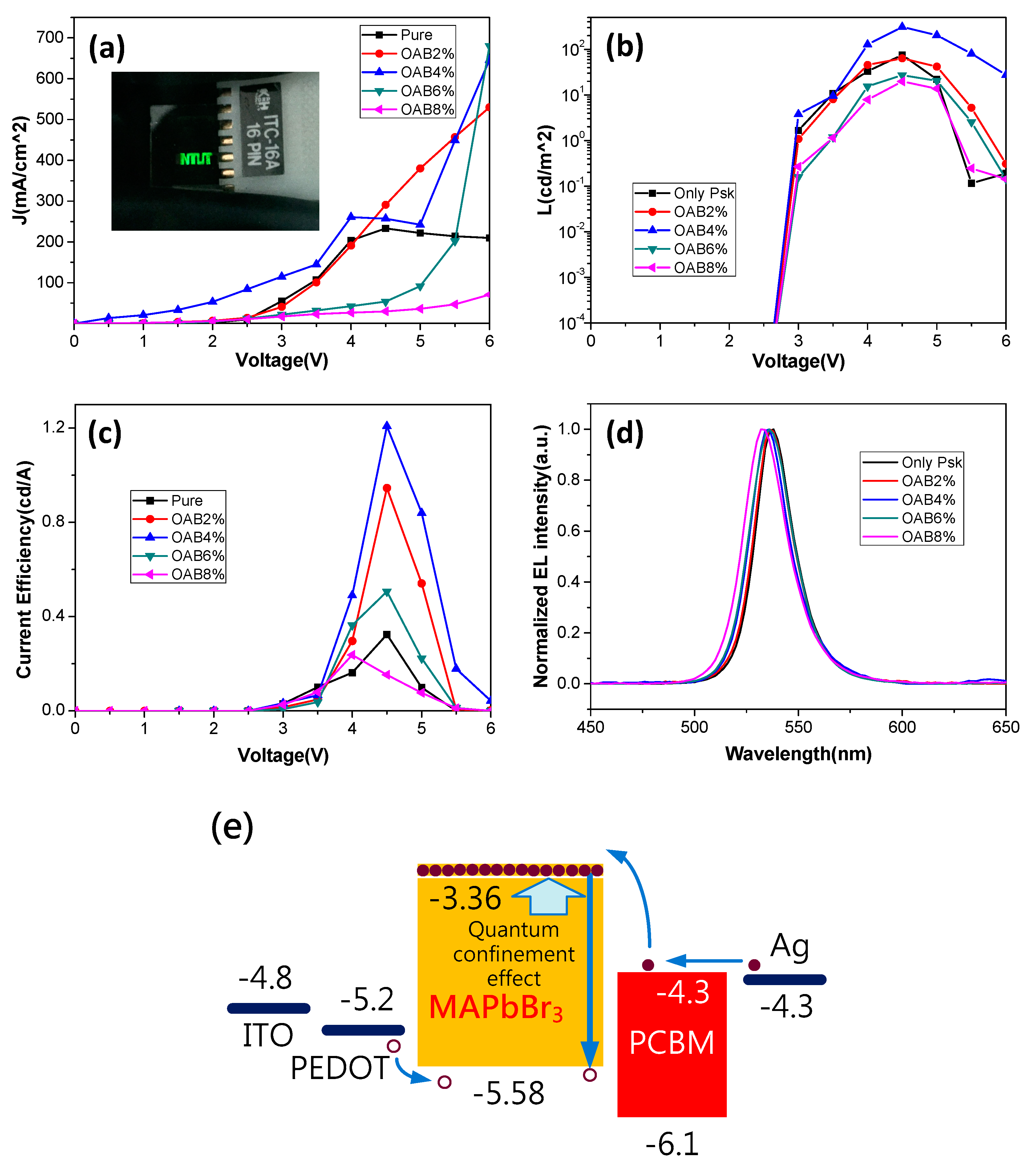
Figure 6.
Temperature-dependent photoluminescence spectra for MAPbBr3 film with an OAB ratio of 4% and without OAB.
Figure 6.
Temperature-dependent photoluminescence spectra for MAPbBr3 film with an OAB ratio of 4% and without OAB.
© 2018 by the authors. Licensee MDPI, Basel, Switzerland. This article is an open access article distributed under the terms and conditions of the Creative Commons Attribution (CC BY) license (http://creativecommons.org/licenses/by/4.0/).
Share and Cite
MDPI and ACS Style
Chen, L.-C.; Tseng, Z.-L.; Lin, D.-W.; Lin, Y.-S.; Chen, S.-H. Improved Performance of Perovskite Light-Emitting Diodes by Quantum Confinement Effect in Perovskite Nanocrystals. Nanomaterials 2018, 8, 459. https://doi.org/10.3390/nano8070459
AMA Style
Chen L-C, Tseng Z-L, Lin D-W, Lin Y-S, Chen S-H. Improved Performance of Perovskite Light-Emitting Diodes by Quantum Confinement Effect in Perovskite Nanocrystals. Nanomaterials. 2018; 8(7):459. https://doi.org/10.3390/nano8070459
Chicago/Turabian StyleChen, Lung-Chien, Zong-Liang Tseng, Dai-Wei Lin, Yu-Shiang Lin, and Sheng-Hui Chen. 2018. "Improved Performance of Perovskite Light-Emitting Diodes by Quantum Confinement Effect in Perovskite Nanocrystals" Nanomaterials 8, no. 7: 459. https://doi.org/10.3390/nano8070459
Note that from the first issue of 2016, this journal uses article numbers instead of page numbers. See further details here.