1. Introduction
Amorphous oxide semiconductor thin-film transistors (AOS-TFTs) as candidates for silicon-based TFTs have come into the spotlight of flat panel display (FPD) because of their low processing temperature, high transparency, high carrier mobility, and good uniformity [
1,
2,
3]. In 2012, the implementation of mass production of FPD with the amorphous In–Ga–Zn–O (a-IGZO) TFT backplane was a milestone for the development of AOS-TFTs [
4]. The requirements of high-resolution, large-size, and narrow border displays are pursued with the advances in display technology. For achieving these requirements, miniaturized TFT with a suitable structure, a high mobility, and a low contact resistivity should be fabricated, which could eliminate image distortion and shading effects during operation. In the conventional AOS-TFTs structure, an etch stopper layer (ESL) should be inserted between the semiconductor and the source/drain (S/D) electrodes to protect the channel layer from damage during the etching of the S/D electrodes. The miniaturized device can be hardly fabricated by this ESL configuration. Compared to the ESL configuration, a TFT with a back-channel-etched (BCE) structure is preferable to achieve the miniaturized fabrication of the AOS device. However, most of the AOS are sensitive to weak acid, which would limit their applications to large-size TFT backplanes. Fortunately, acid-resistant SnO
2 has been suggested as a potential candidate, and the device can obtain a high mobility because of the electronic configuration of the tin ions and indium ions. In previous work, the feasibility of silicon-doped tin oxide (a-STO) TFTs with BCE structure has been demonstrated [
5]. However, the contact characteristics of a-STO TFTs are still unknown. Therefore, it is very necessary to investigate the contact properties of a-STO with different electrodes and facilitate its practical industrial application.
Until now, some interesting phenomena related to the contact properties of AOS-TFTs, such as self-formed metal-oxide contact interlayer [
6,
7] and metal atom diffusion [
8] or migration [
9], have been reported in detail. However, there is no in-depth understanding about how S/D electrodes affect the device performance. Therefore, it is significant to explore whether the S/D electrode could affect the density of states (DOS) of a device. In AOS devices, the subgap DOS is an important parameter which plays a major part in controlling the mobility, operation voltage, and subthreshold swing of TFTs [
10]. Up to now, many extraction methods of DOS based on AOS-TFTs have been developed in numerous studies. For example, Kimura et al. directly extracted the DOS on the basis of the numerical iterative solution of Poisson’s equation by fitting the measured and calculated capacitance–voltage (C–V) characteristics of a-IGZO TFTs at extremely low frequencies, in which the free carrier density had not been taken into account [
11]. Park et al. have proposed the extraction method of acceptor-like DOS of a-IGZO TFTs by combining subgap optical charge pumping and C–V characteristics and verified the measured characteristics compared with Technology Computer Aided Design (TCAD) simulation results incorporating the extracted DOS [
12]. Bae et al. have proposed a physics-based generation–recombination current spectroscopy of n-channel a-IGZO TFTs for extracting the deep donor-like DOS, which is verified by comparing the calculated generation–recombination current with the measured one [
13]. Chen et al. calculated the DOS of a-IGZO TFTs by a straightforward method based on temperature-dependent field-effect measurements in consideration of the Meyer–Neldel rule [
14]. However, the instability of TFTs caused by illumination or thermal effect was ignored during the extraction of the density of states. Consulting the abovementioned methods, a viable and effective method was adopted to extract the DOS of a-STO TFTs.
In this paper, the contact characteristics of a-STO TFTs with different S/D electrodes, including ITO and Mo, were studied. For the first time, the DOS of acceptor-like states in a-STO TFTs was extracted by using low-frequency C–V characteristics.
2. Materials and Methods
TFTs with BCE structure were fabricated on a glass substrate. A 300-nm-thick Al–Nd alloy (3 wt % of Nd) as gate metal was deposited by direct current (DC) magnetron sputtering, and its patterns were defined by photolithography. Then, the Al–Nd alloy film was anodized to form a 200 nm dielectric layer of AlOx–Nd on the surface in an electrolyte consisting of 3.68 wt % ammonium tartrate solution and ethylene glycol. Afterwards, a 5-nm-thick a-STO film was deposited by radio frequency (RF) magnetron sputtering (SNTEK) with a SiSnO (SiO2/SnO2 = 5:95 wt %) ceramic target on the dielectric anodized alumina. For the S/D electrodes, ITO (150 nm) and Mo (200 nm) were deposited by DC magnetron sputtering at room temperature, and the channel length/width (100/30 μm) was patterned by a wet etching process. All the devices were subjected to thermal annealing at 350 °C on a hotplate for 0.5 h in ambient air. At last, a passivation layer of SiO2 (300 nm) was deposited by using a plasma-enhanced chemical vapor deposition (PECVD). In order to obtain high performance of the a-STO TFTs, the devices were annealed at 450 °C for 0.5 h in a protective argon ambient.
The thickness of a-STO films deposited on the glass substrate were measured by X-ray reflectivity (XRR, Empyrean, PANalytical, Almelo, The Netherlands) (See in
Figure S1 and Table S1). The electrical characteristics of TFTs were measured using a semiconductor parameter analyzer (Agilent, 4155C, Santa Clara, CA, USA) in the dark in ambient air. The positive gate bias stress (PBS) stability of the devices were measured under the following conditions:
VGS =
VDS = 30 V. The capacitance versus voltage (C–V) curve of a-STO TFTs was measured by a KEYSIGHT E4990A Impedance Analyzer (Keysight Technologies Inc., Santa Rosa, CA, USA) with a frequency of 10k Hz. The device simulation was performed by the 2D device simulator ATLAS (Silvaco Inc., Santa Clara, CA, USA). The properties of the channel region of the device and Mo/a-STO interface were analyzed by transmission electron microscope (TEM, Bruker, Adlershof, Berlin, Germany) (See in
Figures S2 and S3).
3. Results and Discussion
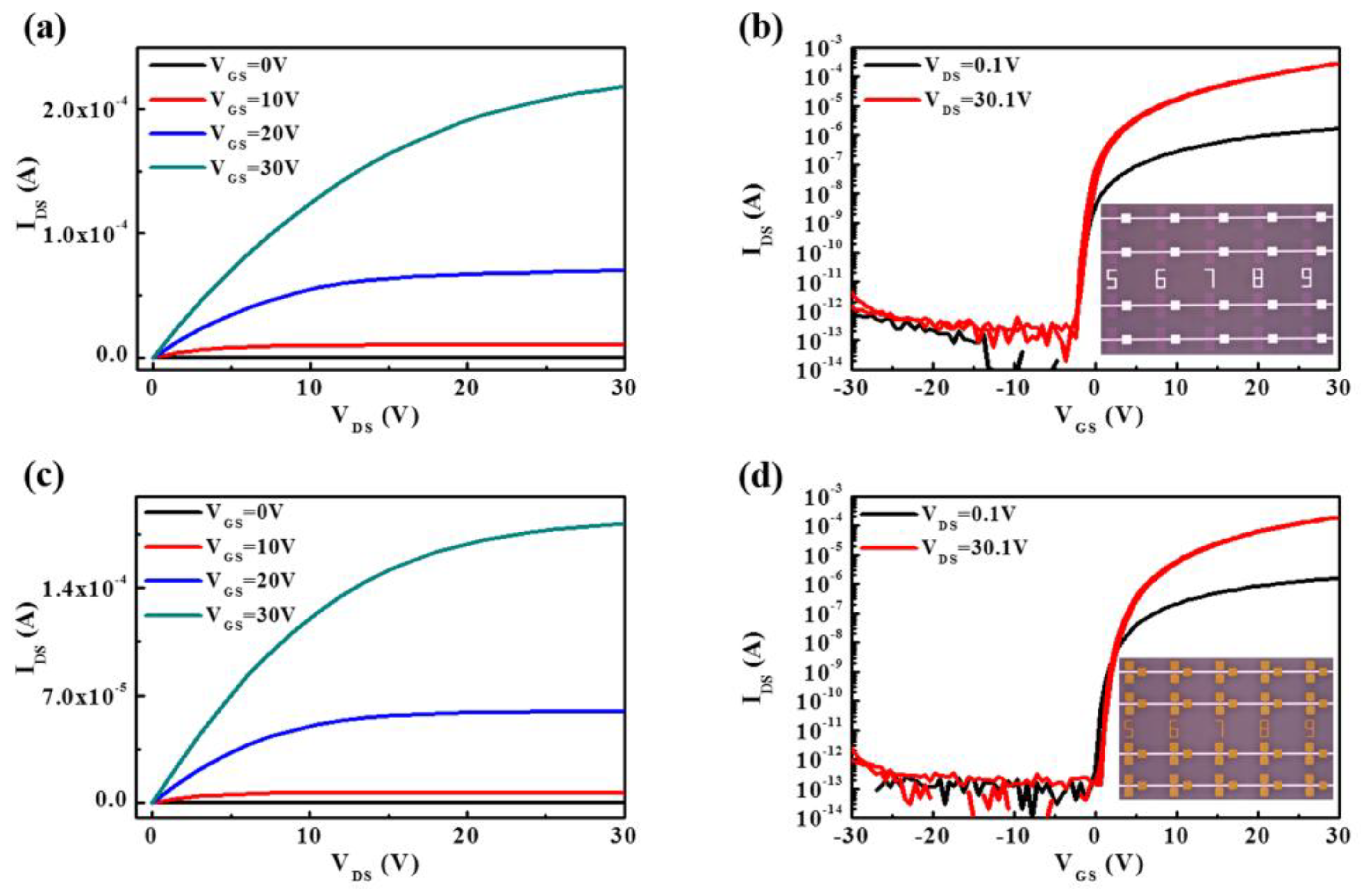
Figure 1 shows the representative output and transfer characteristic curves of a-STO TFTs with ITO and Mo as S/D electrodes. TFTs with ITO and Mo contact showed excellent drain current characteristics without current crowding, which indicated that Ohmic contact could be formed at the electrode/a-STO interface. A good transfer curve of ITO or Mo without hysteresis could be obtained. Thus, the field effect mobility (
μFE) in the linear region and the saturated mobility (
μsat) in the saturation region of the device were extracted by using the following Equations: [
2]
where
VDS is the drain voltage,
VGS is the gate voltage,
Vth is the threshold voltage,
W/
L is the channel width/length, and
Ci is the gate capacitance per unit area of the insulator layer. The subthreshold swing (
SS) could be calculated using the following Equation: [
3]
To ensure the actual level of the electrical properties of the devices with different electrodes contact, four devices were randomly chosen and measured for each S/D electrode material. The electrical parameters of the devices, including field-effect mobility (
μFE), saturation mobility (
μsat), turn-on voltage (
Von), on/off current ratio (
Ion/
Ioff), and subthreshold swing (SS) are list in
Table 1. The
μFE of the a-STO TFTs were 5.6 ± 0.9 cm
2/V s (ITO) and 5.4 ± 0.2 cm
2/V s (Mo). Theoretically, Ohmic contact would be formed in the two devices on the basis of the energy band structure of a-STO film in contact with ITO and Mo (see in
Figures S4 and S5). In consideration of all devices subjected to the same thermal annealing process, the slight difference of electrical characteristics of the two devices was originated in the contact quality at the S/D electrode–a-STO interface.
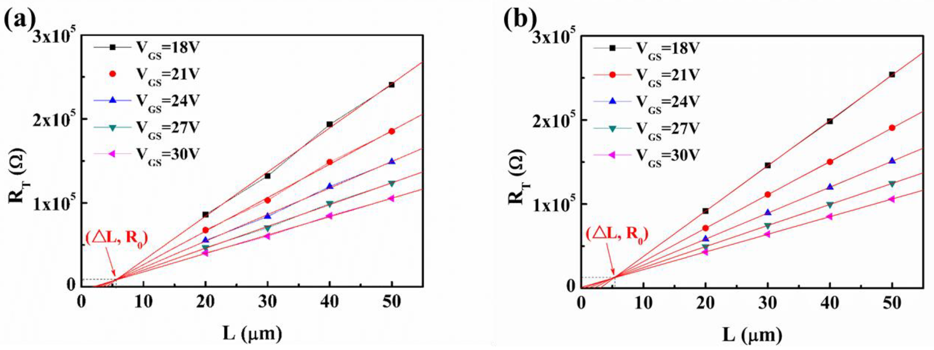
To analyze the reasons for the variation of the electrical characteristics of the a-STO TFTs, the contact properties between a-STO and the electrode were examined using the transmission line method (TLM) [
15]. The total resistance (
RT) as a function of channel length (
L = 20, 30, 40, and 50 μm) for different
VGS values were plotted, and then the experimental values were fit linearly for each
VGS value, as illustrated in
Figure 2. The
Rch and
RSD were extracted by the following Equation (4) in the linear regime:
where
RT is the total resistance,
Rch is the channel resistance per unit channel length,
RSD is the series resistance at the S/D contacts,
Ci is the capacitance per unit area,
μFE-i is the intrinsic field-effect mobility,
L is the physical channel length, and ∆
L is the difference between the effective channel length and the physical channel length (
L) at the S/D contact. Interestingly, an intersection point, providing the resistance (
R0 = 0.5
RSD) value and ∆L, was found in a-STO TFTs with ITO and Mo electrodes, respectively. The
R0/∆
L was 4193.7 Ω/2.81 μm (ITO) and 5871.1 Ω/2.54 μm (Mo). On the basis of Equation (4),
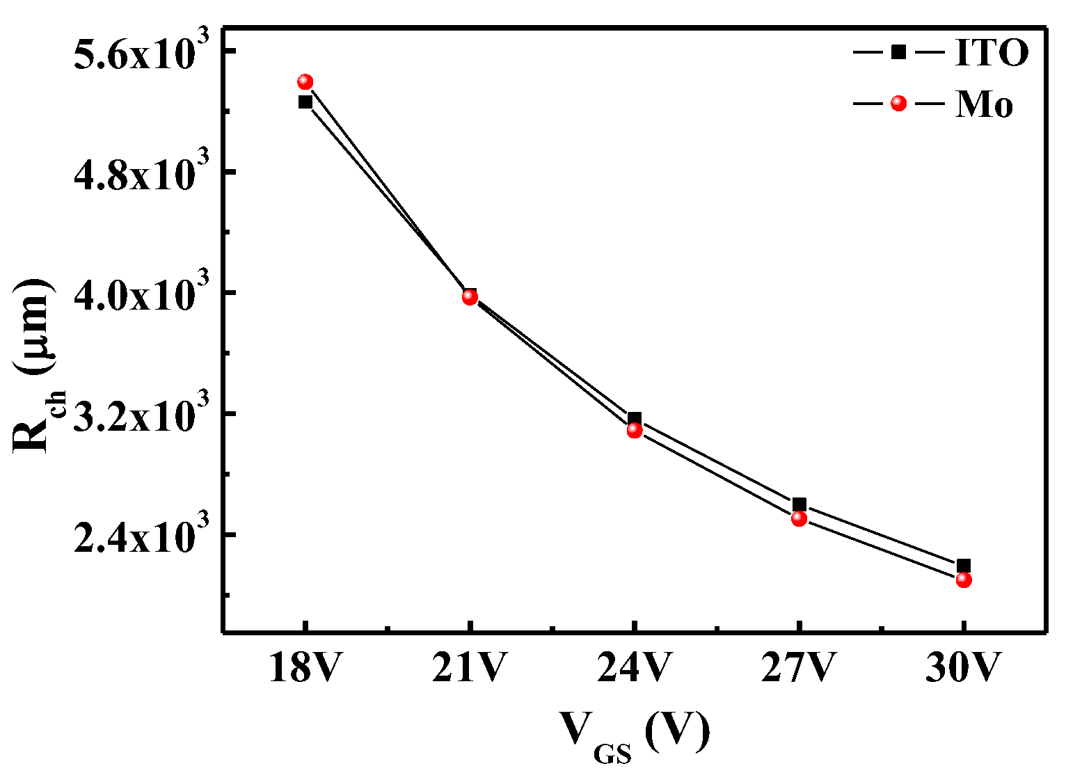
Rch is obtained from the slope. By plotting the
Rch of a-STO TFTs with ITO and Mo electrodes as a function of
VGS, two curves were nearly identical, as shown in
Figure 3. This indicated that the consistency of the channel layer’s property could be guaranteed in the two devices. Herein, the different electrical performances of a-STO TFTs were caused by the contact resistance.
Nevertheless, it was a macro-explanation for the difference of the electrical performances of devices with different S/D electrode contacts. As known to all, the intrinsic properties of AOS-TFTs are attributed to subgap DOS. Therefore, it is meaningful to investigate the DOS of a-STO TFTs to further understand the influence of the electrodes on the device performance. The DOS of a device with different electrodes are extracted by using an analytical and simple method avoiding various complex extraction methods, such as numerical iterative solutions, temperature-dependent characteristics, or multi-frequency C–V characteristics. This simple method considers the low-frequency C–V characteristics of TFTs, which can be obtained by a small AC signal superimposed to the DC bias voltage in the condition of source and drain electrodes connected together [
16].
Figure 4a shows the gate capacitance versus the gate voltage (
CGS-
VGS) characteristics of same dimension a-STO TFTs with ITO and Mo electrodes. The flat band voltage
Vfb can be extracted by the I–V and C–V characteristics, following the method developed by Migliorato et al. [
17]
Figure 4b shows the DOS with respect to (
E-
EC) plot for a device with different electrodes contact (
E is the state energy and
EC is the conduction band minimum). It was found that the distribution for the trap densities of states far from the
EC was quite flat in the energy gap for such metal oxide TFTs, but became larger near the
EC. The DOS of a-STO TFTs could be divided into two parts: deep states and tail states. The plots were approximately fitted using the following superposition of the exponential tail states and exponential deep states:
where
NDA/
NTA is the density of deep/tail states at the conduction edge, and
EDA/
ETA is the characteristics energy of deep/tail states. The
NDA/
NTA is extracted by extrapolating the deep/tail states to
E =
EC, while
EDA/
ETA is extracted from the slope of log(
Nt) versus (
E-
EC) for the deep/tail states. In the AOS, the tail states are caused by structural disorder, which is characterized by a sharp conduction band tail slope because of the large overlapping s orbitals of the heavy cation. The deep states can be originated in excess oxygen in the thin film which forms deep acceptor states [
18], because excess oxygen in the thin film can capture the electrons through
and/or
. The extracted values of the DOS with different electrodes are list in
Table 2. In consideration of the near consistency of the results in
Figure 3, the DOS of both devices could be speculated to be the same. However, it was clearly found that the deep/tail states’ densities of the a-STO TFTs with ITO contact were 6.5 × 10
15/1.7 × 10
17 cm
−3 eV
−1, which was significantly lower than those with Mo contact (8.5 × 10
16/9.5 × 10
18 cm
−3 eV
−1). Considering the almost identical
SS values of the two devices, the different DOS was caused by the generation of local defect states near the electrode. The local defect states might be originated by two factors: (1) the formation of dangling bonds at the electrode–a-STO interface; in fact, on the basis the BDE of Mo-O (597 kJ/mol), Sn-O (528 kJ/mol), and In-O (346 kJ/mol), the electrode could bond with oxygen from a-STO during the high-temperature annealing process, which would result in dangling bonds that can cause various defect states [
19]. A slight difference in the
μFE of the two devices was primarily attributed to the existence of dangling bonds at the electrode/a-STO interface; (2) the generation of hot electrons during the operation of the device. The acceptor-like defect states were formed by hot electrons in the channel when a high
VDS was applied, which could capture the electrons. There was a distinction in the
μsat of two devices, which was mainly ascribed to the generation of different magnitudes of acceptor-like defect states that could hinder the flow of electrons [
20,
21].
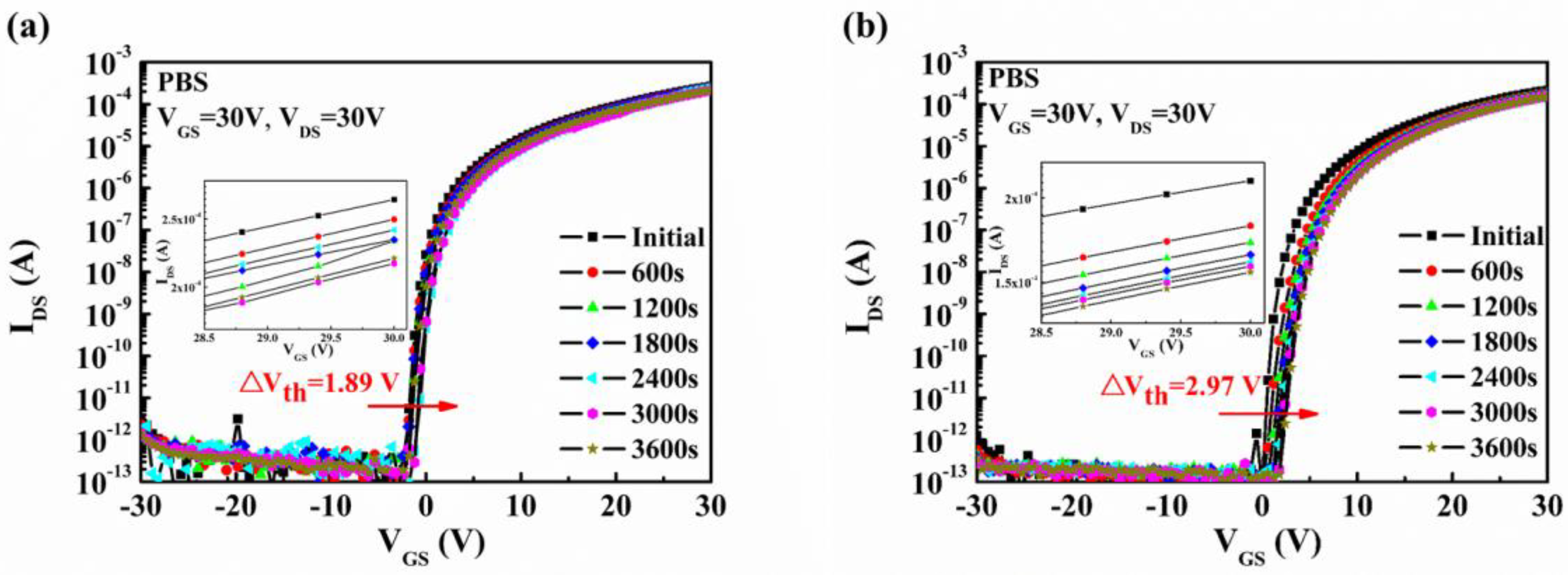
At last, the stabilities of a-STO TFTs with ITO and Mo were investigated by positive gate bias stress (PBS), as shown in
Figure 5. The devices were stressed under the condition
VGS =
VDS = 30 V, which was applied for 3600 s. In the case of PBS stability, the TFT with ITO contact (∆
Vth = 1.89 V) exhibited a more stable behavior than that with Mo contact (∆
Vth = 2.97 V). The reason for the positive shifts of
Vth is generally the trapping of electrons at the gate insulator–semiconductor interface. Interestingly, the on-current of both devices decreased as the time increased. This, again, implied that the generation of the local defect states near the electrode, resulting in the formation of a potential barrier, could block the injection of electrons from the electrode.

 ,
, 

