High-Efficiency, Near-Diffraction Limited, Dielectric Metasurface Lenses Based on Crystalline Titanium Dioxide at Visible Wavelengths


 ,
, 
Abstract
:
1. Introduction
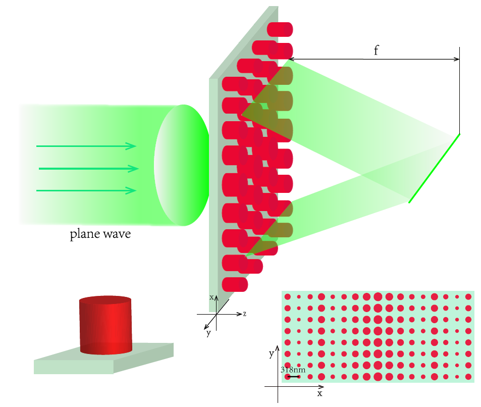
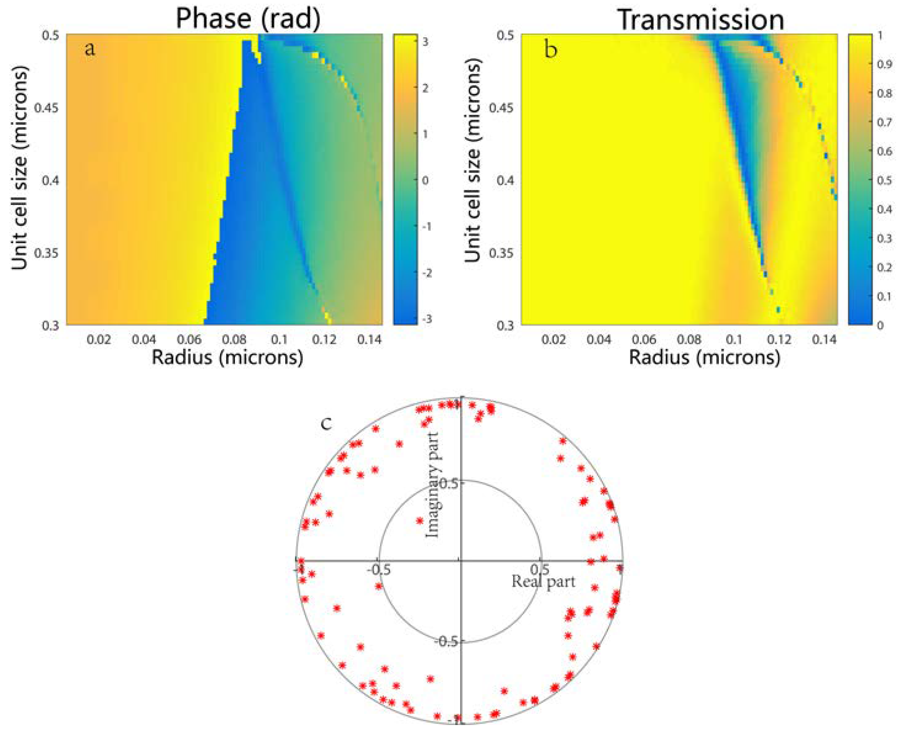
2. Methods
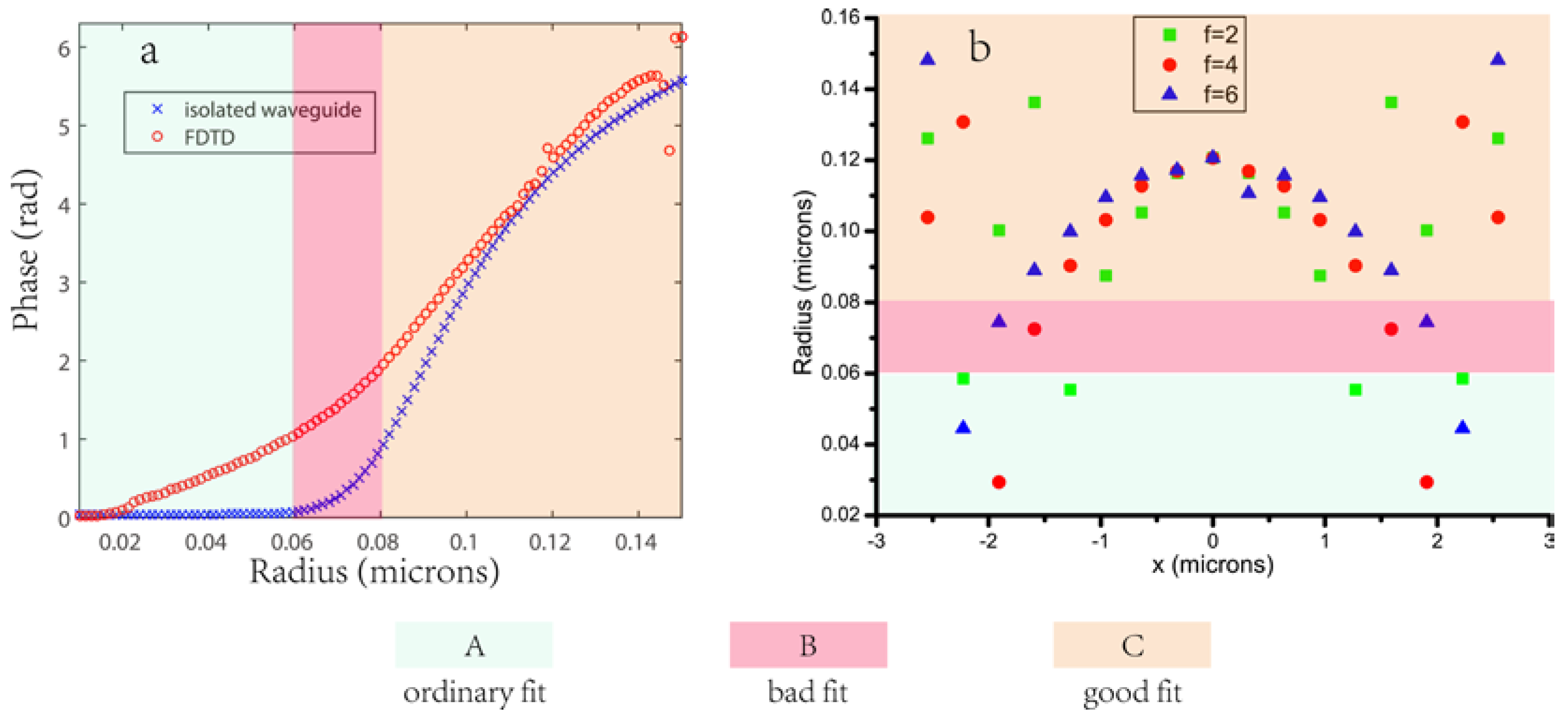
3. Results and Discussion
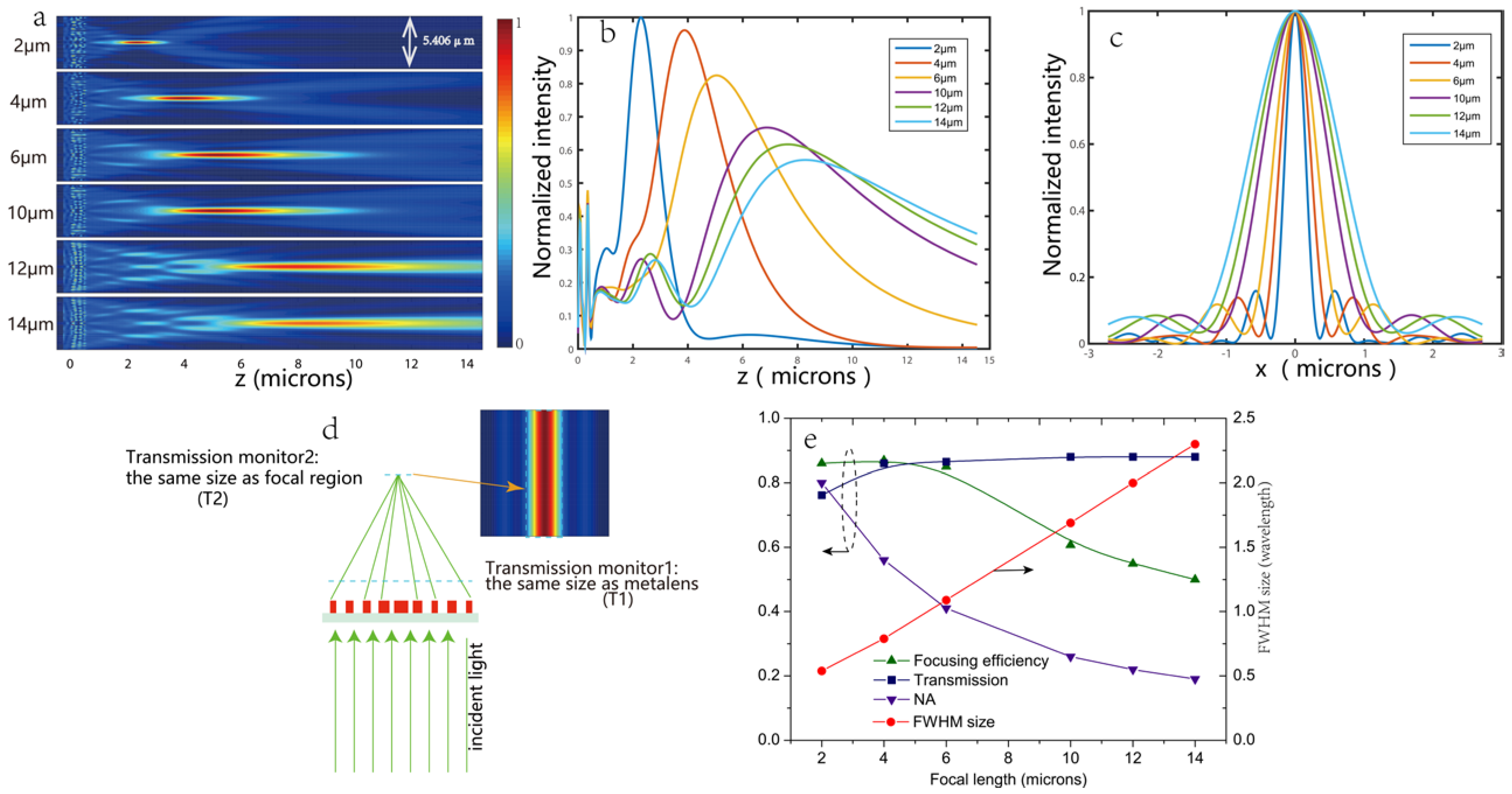
3.1. The Focal Length Dependence at the Design Wavelength of 633 nm
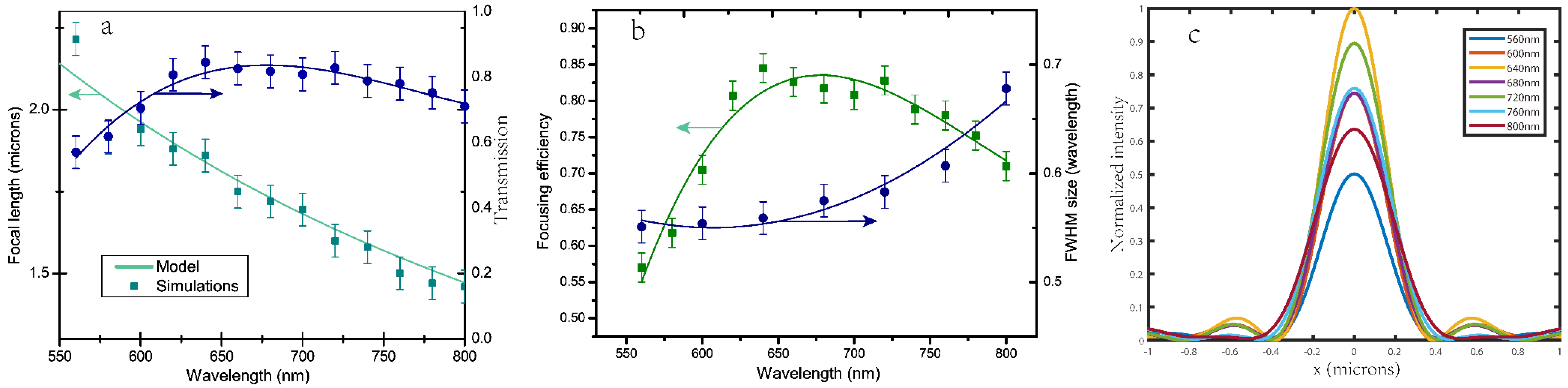
3.2. The Broadband Characteristics
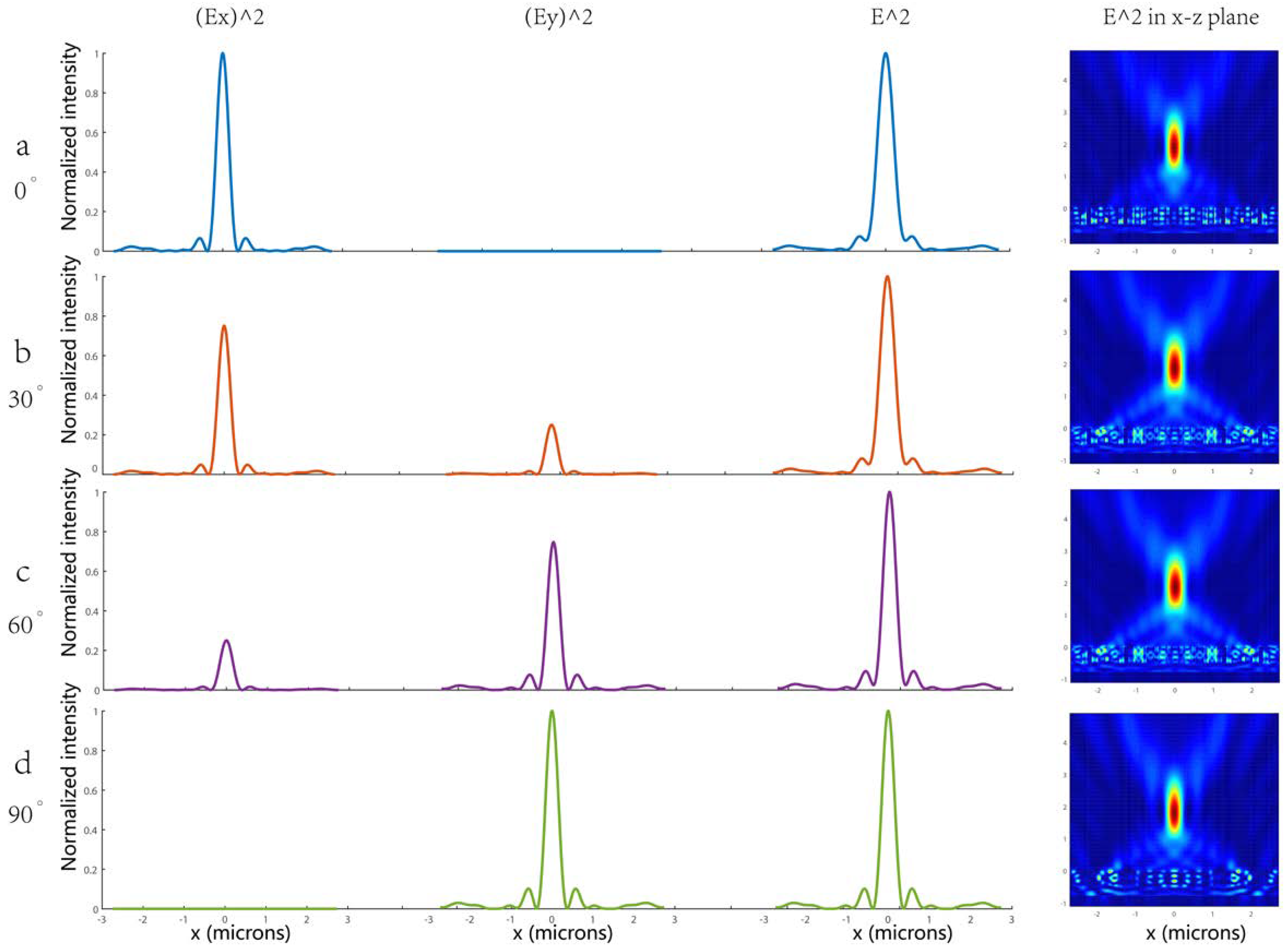
3.3. Insensitive to Incident Polarizations
4. On- and Off-Axis Imaging
5. Conclusions
Supplementary Materials
Author Contributions
Acknowledgments
Conflicts of Interest
References
- Kildishev, A.V.; Boltasseva, A.; Shalaev, V.M. Planar photonics with metasurfaces. Science 2013, 339, 1232009. [Google Scholar] [CrossRef] [PubMed]
- Yu, N.; Capasso, F. Flat optics with designer metasurfaces. Nat. Mater. 2014, 13, 139–150. [Google Scholar] [CrossRef] [PubMed]
- Yu, N.; Genevet, P.; Kats, M.A.; Aieta, F.; Tetienne, J.-P.; Capasso, F.; Gaburro, Z. Light Propagation with Phase Discontinuities: Generalized Laws of Reflection and Refraction. Science 2011, 334, 333–337. [Google Scholar] [CrossRef] [PubMed]
- Lin, D.; Fan, P.; Hasman, E.; Brongersma, M.L. Dielectric gradient metasurface optical elements. Science 2014, 345, 298–302. [Google Scholar] [CrossRef] [PubMed]
- Aieta, F.; Genevet, P.; Kats, M.A.; Yu, N.; Blanchard, R.; Gaburro, Z.; Capasso, F. Aberration-free ultrathin flat lenses and axicons at telecom wavelengths based on plasmonic metasurfaces. Nano Lett. 2012, 12, 4932–4936. [Google Scholar] [CrossRef] [PubMed]
- Hu, D.; Wang, X.; Feng, S.; Ye, J.; Sun, W.; Kan, Q.; Klar, P.J.; Zhang, Y. Ultrathin Terahertz Planar Elements. Adv. Opt. Mater. 2013, 1, 186–191. [Google Scholar] [CrossRef]
- Jiang, X.Y.; Ye, J.S.; He, J.W.; Wang, X.K.; Hu, D.; Feng, S.F.; Kan, Q.; Zhang, Y. An ultrathin terahertz lens with axial long focal depth based on metasurfaces. Opt. Express 2013, 21, 30030–30038. [Google Scholar] [CrossRef] [PubMed]
- Kang, M.; Feng, T.; Wang, H.T.; Li, J. Wave front engineering from an array of thin aperture antennas. Opt. Express 2012, 20, 15882–15890. [Google Scholar] [CrossRef] [PubMed]
- Ma, W.; Jia, D.; Yu, X.; Feng, Y.; Zhao, Y. Reflective gradient metasurfaces for polarization-independent light focusing at normal or oblique incidence. Appl. Phys. Lett. 2016, 108, 071111. [Google Scholar] [CrossRef]
- Wang, W.; Guo, Z.; Li, R.; Zhang, J.; Li, Y.; Liu, Y.; Wang, X.; Qu, S. Plasmonics metalens independent from the incident polarizations. Opt. Express 2015, 23, 16782–16791. [Google Scholar] [CrossRef] [PubMed]
- Pors, A.; Nielsen, M.G.; Eriksen, R.L.; Bozhevolnyi, S.I. Broadband focusing flat mirrors based on plasmonic gradient metasurfaces. Nano Lett. 2013, 13, 829–834. [Google Scholar] [CrossRef] [PubMed]
- Guo, Z.; Zhu, L.; Shen, F.; Zhou, H.; Gao, R. Dielectric metasurface based high-efficiency polarization splitters. RSC Adv. 2017, 7, 9872–9879. [Google Scholar] [CrossRef]
- Khorasaninejad, M.; Shi, Z.; Zhu, A.Y.; Chen, W.T.; Sanjeev, V.; Zaidi, A.; Capasso, F. Achromatic Metalens over 60 nm Bandwidth in the Visible and Metalens with Reverse Chromatic Dispersion. Nano Lett. 2017, 17, 1819–1824. [Google Scholar] [CrossRef] [PubMed]
- Bomzon, Z.; Biener, G.; Kleiner, V.; Hasman, E. Space-variant Pancharatnam-Berry phase optical elements with computer-generated subwavelength gratings. Opt. Lett. 2002, 27, 1141. [Google Scholar] [CrossRef] [PubMed]
- Khorasaninejad, M.; Crozier, K.B. Silicon nanofin grating as a miniature chirality-distinguishing beam-splitter. Nat. Commun. 2014, 5, 5386. [Google Scholar] [CrossRef] [PubMed]
- Yang, Y.; Wang, W.; Moitra, P.; Kravchenko, I.I.; Briggs, D.P.; Valentine, J. Dielectric meta-reflectarray for broadband linear polarization conversion and optical vortex generation. Nano Lett. 2014, 14, 1394–1399. [Google Scholar] [CrossRef] [PubMed]
- Ding, X.; Monticone, F.; Zhang, K.; Zhang, L.; Gao, D.; Burokur, S.N.; de Lustrac, A.; Wu, Q.; Qiu, C.W.; Alù, A. Ultrathin pancharatnam-berry metasurface with maximal cross-polarization efficiency. Adv. Mater. 2015, 27, 1195–1200. [Google Scholar] [CrossRef] [PubMed]
- Ma, X.; Pu, M.; Li, X.; Huang, C.; Wang, Y.; Pan, W.; Zhao, B.; Cui, J.; Wang, C.; Zhao, Z.; et al. A planar chiral meta-surface for optical vortex generation and focusing. Sci. Rep. 2015, 5, 10365. [Google Scholar] [CrossRef] [PubMed]
- Khorasaninejad, M.; Chen, W.T.; Devlin, R.C.; Oh, J.; Zhu, A.Y.; Capasso, F. Metalenses at visible wavelengths: Diffraction-limited focusing and subwavelength resolution imaging. Science 2016, 352, 1190–1194. [Google Scholar] [CrossRef] [PubMed]
- Fan, Q.; Huo, P.; Wang, D.; Liang, Y.; Yan, F.; Xu, T. Visible light focusing flat lenses based on hybrid dielectric-metal metasurface reflector-arrays. Sci. Rep. 2017, 7, 45044. [Google Scholar] [CrossRef] [PubMed]
- Khorasaninejad, M.; Aieta, F.; Kanhaiya, P.; Kats, M.A.; Genevet, P.; Rousso, D.; Capasso, F. Achromatic Metasurface Lens at Telecommunication Wavelengths. Nano Lett. 2015, 15, 5358–5362. [Google Scholar] [CrossRef] [PubMed]
- Kamali, S.M.; Arbabi, E.; Arbabi, A.; Horie, Y.; Faraon, A. Highly tunable elastic dielectric metasurface lenses. Laser Photonics Rev. 2016, 10, 1002–1008. [Google Scholar] [CrossRef]
- Khorasaninejad, M.; Chen, W.T.; Zhu, A.Y.; Oh, J.; Devlin, R.C.; Rousso, D.; Capasso, F. Multispectral Chiral Imaging with a Metalens. Nano Lett. 2016, 16, 4595–4600. [Google Scholar] [CrossRef] [PubMed]
- Lalanne, P.; Chavel, P. Metalenses at visible wavelengths: Past, present, perspectives. Laser Photonics Rev. 2017, 11, 1600295. [Google Scholar] [CrossRef]
- Khorasaninejad, M.; Zhu, A.Y.; Roques-Carmes, C.; Chen, W.T.; Oh, J.; Mishra, I.; Devlin, R.C.; Capasso, F. Polarization-Insensitive Metalenses at Visible Wavelengths. Nano Lett. 2016, 16, 7229–7234. [Google Scholar] [CrossRef] [PubMed]
- Yariv, A.; Yeh, P. Photonics: Optical Electronics in Modern Communications (the Oxford Series in Electrical and Computer Engineering), 6th ed.; Oxford University Press: New York, NY, USA, 2007. [Google Scholar]
- Khorasaninejad, M.; Capasso, F. Broadband Multifunctional Efficient Meta-Gratings Based on Dielectric Waveguide Phase Shifters. Nano Lett. 2015, 15, 6709–6715. [Google Scholar] [CrossRef] [PubMed]


© 2018 by the authors. Licensee MDPI, Basel, Switzerland. This article is an open access article distributed under the terms and conditions of the Creative Commons Attribution (CC BY) license (http://creativecommons.org/licenses/by/4.0/).
Share and Cite
Liang, Y.; Liu, H.; Wang, F.; Meng, H.; Guo, J.; Li, J.; Wei, Z. High-Efficiency, Near-Diffraction Limited, Dielectric Metasurface Lenses Based on Crystalline Titanium Dioxide at Visible Wavelengths. Nanomaterials 2018, 8, 288. https://doi.org/10.3390/nano8050288
Liang Y, Liu H, Wang F, Meng H, Guo J, Li J, Wei Z. High-Efficiency, Near-Diffraction Limited, Dielectric Metasurface Lenses Based on Crystalline Titanium Dioxide at Visible Wavelengths. Nanomaterials. 2018; 8(5):288. https://doi.org/10.3390/nano8050288
Chicago/Turabian StyleLiang, Yaoyao, Hongzhan Liu, Faqiang Wang, Hongyun Meng, Jianping Guo, Jinfeng Li, and Zhongchao Wei. 2018. "High-Efficiency, Near-Diffraction Limited, Dielectric Metasurface Lenses Based on Crystalline Titanium Dioxide at Visible Wavelengths" Nanomaterials 8, no. 5: 288. https://doi.org/10.3390/nano8050288