A Perspective on the Application of Spatially Resolved ARPES for 2D Materials


1
School of Chemistry, University of Bristol, Cantocks Close, Bristol BS8 1TS, UK; [email protected]
2
H. H. Wills Physics Laboratory, University of Bristol, Tyndall Avenue, Bristol BS8 1TL, UK
*
Author to whom correspondence should be addressed.
Nanomaterials 2018, 8(5), 284; https://doi.org/10.3390/nano8050284
Submission received: 11 April 2018
/
Revised: 20 April 2018
/
Accepted: 23 April 2018
/
Published: 27 April 2018
(This article belongs to the Special Issue Synthesis, Structure and Applications of 2D Nanomaterials)
Abstract
:In this paper, a perspective on the application of Spatially- and Angle-Resolved PhotoEmission Spectroscopy (ARPES) for the study of two-dimensional (2D) materials is presented. ARPES allows the direct measurement of the electronic band structure of materials generating extremely useful insights into their electronic properties. The possibility to apply this technique to 2D materials is of paramount importance because these ultrathin layers are considered fundamental for future electronic, photonic and spintronic devices. In this review an overview of the technical aspects of spatially localized ARPES is given along with a description of the most advanced setups for laboratory and synchrotron-based equipment. This technique is sensitive to the lateral dimensions of the sample. Therefore, a discussion on the preparation methods of 2D material is presented. Some of the most interesting results obtained by ARPES are reported in three sections including: graphene, transition metal dichalcogenides (TMDCs) and 2D heterostructures. Graphene has played a key role in ARPES studies because it inspired the use of this technique with other 2D materials. TMDCs are presented for their peculiar transport, optical and spin properties. Finally, the section featuring heterostructures highlights a future direction for research into 2D material structures.
1. Introduction
The field of two-dimensional (2D) material research began with the discovery of graphene in 2004 [1,2], which seeded the exploration of many new 2D systems. The common features of this group of materials are their extremely small thickness, typically a few atomic layers, with strong in-plane bonds and weak interlayer bonds. Two-dimensional materials are very important in modern technology because of their amazing physical and chemical properties; they are regarded as the thinnest functional materials.
The family of 2D materials covers the complete range of electrical proprieties from superconducting to insulating [3,4,5,6]. A powerful tool to investigate their properties is Angle-Resolved PhotoEmission Spectroscopy (ARPES). This photoemission technique exploits the emission of photo excited electrons from a crystalline sample by a photon source illuminating the surface. ARPES from conventional light sources allows the probing of the filled states in a material and the direct measurement of its electronic band structure, which is generated by the allowed quantum mechanical wave functions for an electron in a periodic lattice of atoms. Due to the electron momentum sensitivity of the ARPES technique, important characteristics of the materials can be measured such as electron effective mass, Fermi velocity, the Valence Band Maximum (VBM) energy and its position, doping, and many-body effects.
In this review the preparation methods employed to produce 2D material are discussed briefly, and include Chemical Vapor Deposition (CVD) [7], Physical Vapor Deposition (PVD) [8], and mechanical exfoliation. The latter is the easiest way to prepare high-quality 2D materials in a laboratory; it can be applied to the most innovative materials because it is possible as soon as small bulk pieces of a material are produced. The exfoliated flakes typically have micrometric lateral dimensions, but it is difficult to thin down the material to a single layer homogenously. However, the sampling area of a conventional ARPES experiment ranges from tens of micrometers, at synchrotron ARPES facilities, to millimeters in laboratory facilities and can be the principal limitation on the application of ARPES to exfoliated 2D materials.
An ideal experiment to study the band structure of 2D materials should allow the visualization of the sample in the macro or nanoscale, utilizing a small portion of sample material to obtain ARPES. In the past few years, instrument advances have been made that allow complex measurement operations to be performed at synchrotron light facilities and using laboratory-based equipment. In this review, the operating principles of the spatially localized ARPES systems will be presented. First, an overview of early ARPES measurement setups will be discussed before describing state-of-the-art, spatially resolved ARPES equipment.
This paper features some of the most interesting results obtained to date on graphene, transition metal dichalcogenides (TMDCs), and 2D heterostructures along with discussions about future instrument upgrades for spatially-, spin-, and time-resolved acquisitions. Graphene was a starting point for the investigation by spatially localized ARPES of 2D materials, an example of advanced spatially localized investigations on polycrystalline few layer graphene has been reported [7]. TMDCs have intriguing electronic, spintronic, and photonic properties, and the study of their band structure is of fundamental importance. Examples of the most well-known TMDC, namely, MoS2 [9], and potentially the most innovative such as TiSe2, VSe2 [10], and ReS2 [11,12] are also mentioned. In the section on 2D heterostructures several examples of graphene/TMDC composites are presented. Graphene is often used as an active component of the heterostructure [13] but cases where graphene is employed as protective capping layer [14,15] as well as a conductive substrate [11,15] have also been reported. A rare example of a study on an "all-TMDCs’ heterostructure is presented in this section [15] exemplifying the strength of this technique for the study innovative ultra-thin 2D devices.
2. ARPES Setups: Technical Considerations
2.1. ARPES Technical Considerations
The ARPES technique needs an instrument setup that allows (i) the possibility to investigate the photoemission intensity as function of emission angle and (ii) the ability to distinguish the kinetic energy of the photoelectrons. A sample for ARPES must be crystalline to possess an ordered band structure, and its surface must be smooth to conserve the k-parallel component from the crystal to the vacuum [16]. The surface must also be ultra-clean because the sampling depth is typically only few nanometers. ARPES is therefore performed in ultra-high vacuum (UHV) chambers to analyze a clean surface and to ensure that gas molecules do not scatter the low energy photoelectrons.
In the very first ARPES experiments, the samples were a few millimeters wide and photoelectrons were detected using a hemispherical analyzer with a small acceptance angle and a simple electron counting detector. The role of the electron analyzer is very important; indeed, it is the element that allows one to measure the photoelectron kinetic energy, creating, with the simplest 1D detector, an intensity versus kinetic energy spectrum (Figure 1b). In the early experiments, electron analyzers were also used to select a small solid angle of the whole photoelectron emission cloud, which corresponded to a small portion of the k-space [16]. Samples were illuminated with synchrotron light or discharge lamps over a relatively large and homogenous area, see Figure 1a. When the analyzer was positioned at the sample normal, the photoelectrons emitted from it came from the Γ point i.e., the center of the Brillouin zone, see Figure 1b,e. To perform ARPES the sample had to be rotated in both polar and azimuthal angles so that the electron analyzer acquired photoemission spectra at different angles (Figure 1c). By combining the photoemission signal acquired at different angles a reconstruction of the band structure of the material was obtained.
With 1D detector mapping the acquisition of a full band structure was time-consuming and needed complex sample movements. The introduction of 2D electron detectors provided the means to reduce the number of sample rotations, as illustrated in Figure 1d. Electron analyzers equipped with multichannel plate 2D detectors can discriminate the electron dispersion in the analyzer plane allowing the acquisition of a slice of the k-space, as shown in Figure 1d, e, which can be equivalent to a polar scan with a 1D detector (Figure 1c). This technological improvement drastically increased the quality of spectra obtained and decreased the acquisition times for conventional ARPES. The significance of this advance can be seen by comparing Figure 1c,d.
A recent enhancement to these analyzer systems has enabled angular scans to be made in two dimensions in k-space without tilting or rotating the sample. The scanning of k-space is carried out electronically using dedicated deflectors. An example representation of the region of k-space that can be sampled with these detectors is represented by the orange shaded area in Figure 1e. Consequently, using such electron analyzers, a sector of k-space can be acquired. Using a suitable photon source energy, it is possible to acquire a representative set of high symmetry points without any mechanical movement of the sample. Keeping the sample in the same position during k-space mapping is a crucial requirement for obtaining spatially localized ARPES.
2.2. Spatially Localized ARPES
Considering the complex procedure needed to perform conventional ARPES from large area samples, it is understandable that to perform ARPES on micro- or nano-sized samples poses a significant technical challenge. Instruments need to scan a vast region of the sample surface in real space (X/Y plane) to find the interesting regions, typically microns wide, and then perform ARPES on them. Nowadays there are different setups available to research and industry to be able to do spatially localized ARPES, and the instrument configurations can be divided into the following two categories:
- setups that present extremely small light spots, and where surface mapping is done by moving the sample with respect to the light;
- setups that allow visualization of the real and k-space by extracting electrons using strong electric fields.
For the first category, the spatially-localized ARPES is typically carried out at synchrotron light source facilities, see Figure 2. They differ from classical ARPES beamlines in that the focusing of the beam is done by dedicated focusing elements. Synchrotron light must have a high brightness and photon flux to offset the strong attenuation by the focusing elements.
With these setups it is possible to visualize samples in real space by mounting them on motorized stages (Figure 2) and collecting photoelectrons as function of the sample position. The lateral resolution is directly linked to the beam spot size: the smaller the spot, the better the lateral resolution.
ARPES mapping is acquired either by moving the electron analyzer in UHV over a range of different emission angles, which is the configuration used at the Spectromicroscopy beamline in the Elettra synchrotron [17], or, most commonly, by rotating the sample with respect to a fixed analyzer, as shown by the arrows in Figure 2. The latter configuration introduces the non-trivial issue of keeping the photon beam in the same sample position while rotating the sample but allows the use of a large hemispherical electron analyzers that are not movable under UHV conditions. This setup is employed at the beamlines I05 in Diamond, ANTARES in Soleil [18] and MAESTRO in Advanced Light Source (ALS). All of these facilities refer to spatially localized ARPES as “nano-ARPES” because the light spot can be focused to nanometer-sized spots [19]. The use of state-of-the-art hemispherical electron analyzers with a deflection mode, as in ANTARES, allows the sample to be kept in a fixed position and the measurement of a larger sector of k-space can then be acquired, as seen in Figure 1e.
The synchrotron light source is important not only for the brilliance of the light, but also because it can allow ARPES to be performed at different photon energies and polarizations. Moreover, the broad range of photon energies available allows X-ray photoemission spectroscopy (XPS) to be performed. The ability to perform spatially localized core-level spectroscopy gives a much deeper insight into surface conditions such as composition, oxidation and contamination.
For the second category, the photoelectrons are accelerated by an extractor electrode towards an electron optical column, which contains electrostatic or magnetic electron lenses, corrector elements such as stigmators and deflectors, apertures placed in the image plane and contrast apertures. Such instruments are usually referred to as PhotoEmission Electron Microscopes (PEEMs), see in Figure 3a. These setups can be configured to visualize how the photoelectrons escape from the sample at different angles (in k-space) (Figure 3d,e) and by imaging the sample in real space allow the identification of features of interest (Figure 3b,c). Several field of views are available both for real and reciprocal space operation. Apertures positioned in the image plane are used to select a micron-sized portion of the sample whereas contrast apertures select specific emission angles.
These instruments allow the sample to be imaged without moving it either in real or reciprocal space (Figure 3c,d). This important feature solves major alignment, rotational and movement problems under UHV conditions. Another advantage of these setups is that the zones selected for micro-ARPES as well as the lateral resolution are not dependent on the light spot size, therefore laboratory light sources such as discharge lamps can be used, making it feasible to have PEEM on UHV laboratory-based platforms.
However, a PEEM column cannot filter the photoelectron kinetic energy, therefore it is missing an ARPES measurement requirement. To distinguish the kinetic energy of photoelectrons, PEEMs must be equipped with energy filters that allow one to scan the photoelectron kinetic energy spectrum, these more complex setups are called energy-filtered PEEM (EF-PEEM). The ARPES mapping operation is acquired by imaging at a range of kinetic energies of the full-wavevector landscape (Figure 3d), allowing direct imaging of isoenergetic slices of the band structure (see Figure 3d and yellow dashed plane in Figure 3e). The full 1st Brillouin zone can be acquired without moving the sample in micron-sized areas, see Figure 3d–f. It should be noted that the isoenergetic images, both in the real and reciprocal space, are acquired with no electronic and/or mechanical scanning, but by capturing a single snapshot of the complete field of view presented by the instrument; this ability enables very fast ARPES acquisitions.
Included among the available commercial EF-PEEM instruments are the NanoESCA II and the Time-of-flight (TOF) PEEM of Focus (Focus GmbH, Huenstetten, Germany), the METIS and FE-LEEM (low energy electron microscopy)/PEEM P90 of SPECS (SPECS GmbH, Berlin, Germany), and the ELMITEC PEEM/LEEM (ELMITEC Elektronenmikroskopie GmbH, Clausthal-Zellerfeld, Germany). The energy selection in these instruments is performed in a range of different ways, including using hemispherical analyzer(s), TOF filters and electrostatic/magnetic retarding optics.
The best energy resolutions are obtained by the hemispherical analyzers and TOF, for example NanoESCA II is equipped with two hemispherical analyzers coupled in a “S” fashion to minimize the aberrations [20], and with these setups the achievable energy resolution is typically of the order of few tens of meV. The PEEM/LEEM instruments do not excel in energy resolution, however, they are very versatile instruments and with their electron source they can perform low energy electron diffraction (LEED) in micro-spot mode and visualize single atomic steps [21].
All these instruments have a lateral resolution in the nanometer range, LEEMs in this respect typically out-perform PEEMs, but in any case, spatially localized ARPES is usually performed over an area of a few microns and limited by the fact that the area is selected by means of a mechanical aperture.
Laboratory-based equipment typically use discharge lamps, such as a He lamp that offers 21.2 eV (He I) or 40.8 eV (He II) photon energies. The poor photon tunability does not represent a problem for single layer 2D materials because they do not have a kz dispersion, but it is a limitation for 3D materials where synchrotron tunable radiation must be employed to analyze the kz dispersion. Indeed, several EF-PEEM are installed on synchrotron light source facilities to offer the combination of high flux and versatility of synchrotron light with the fast imaging and stability of the PEEM. Almost all the synchrotron light facilities host a PEEM beamline, among those facilities there are NanoESCA [22] and Nanospectroscopy beamlines in operation at Elettra, I06 at Diamond, HERMES at Soleil, and SIM at PSP.
It is important to note that using a technique called dark-field PEEM a portion in k-space and energy can be selected [23]; this defined element in k-space, e.g., a Dirac cone, can be used as source of signal to image the sample in real space, allowing the identification of the material portion where the k-space feature arises. These acquisitions can be performed with EF-PEEMs [23] and in some nano/micro-ARPES beamlines such as Spectromicroscopy [24] and ANTARES [18].
2.3. ARPES Setups Comparison
The next section is principally focused on spatially localized band structure measurements nonetheless other types of ARPES setups are included in the context of some of the most representative 2D materials. Each type of ARPES setup presents its own pros and cons which are reported in Table 1 along with future technique upgrades.
3. Spatially Resolved ARPES for 2D Materials
Spatially localized ARPES has been developed to allow the analysis of micro- or nanometric samples, consequently it is strongly dependent upon the lateral dimensions of the sample. Several technological challenges arise from the production large flakes of 2D materials, therefore it is important to understand how they can be synthesized. Three different techniques to grow 2D materials have been reported:
- Epitaxial growth by CVD or PVD. This method allows flat and azimuthally oriented layers to be deposited on large single crystal substrates. It is easy to control the number of layers by changing the deposition time, growth chambers can be directly mounted onto ARPES equipment so that samples can be transferred for analysis under UHV conditions. With epitaxial films it is not necessary to employ spatially-resolved ARPES to limit the analyses region on single material grains because the grains are azimuthally oriented with the substrate and form a macroscopic continuous ordered crystalline lattice. Because of the large amount of signal available for ARPES, advanced analyses such as spin-resolved or time-resolved ARPES are feasible on such samples (see in Table 1). There are two main disadvantages of this method: it is time consuming, because evaporators and setups must be carefully optimized for each different material; secondly, the interaction between the substrate and 2D materials is so strong that usually it is not feasible to transfer the 2D layers onto other substrates.
- Conventional CVD produces large micron-scale grains azimuthally misaligned. In respect to the epitaxial growth, the control of the number of layers it is more difficult and occasionally multi-layers are produced. Furthermore, this method is more prone to contamination because it is usually performed under non-UHV conditions. The advantage of conventional CVD with respect to epitaxial growth is that it is possible to use single crystal and polycrystalline substrates with weaker bonds to the 2D material, allowing their detachment and transfer.
- Mechanical exfoliation, also called “adhesive tape technique”, produces extremely high-quality layers because they are peeled from ultra-pure single crystals. The main drawbacks are the micron-sized areas of the layers and that the thickness is not easily controllable. This technique is the main method used for studying promising new 2D materials because it is fast and easily achievable, exploiting the ease of exfoliation along the weak van der Waals inter-layer bonds. Importantly, it is the main technique to form 2D heterostructures.
Not all the materials can be prepared using all three methods. Some analogues of graphene such as silicene [25] and germanene [26], and some TMDCs, such as PtSe2 [27], are obtainable with good quality only by epitaxial methods. Indeed, spatially localized ARPES is ideally suited to the analysis of samples prepared by CVD and mechanical exfoliation. Arguably the most interesting samples for study are the mechanically exfoliated ones, due to their formation in micrometric flakes with multiple layers. These can be used to analyze the changes in band structure and electronic properties with different numbers of layers on a single sample. For the most challenging 2D material analyses, spatially localized ARPES is also used to analyze bulk crystals, which, at the beginning of the material growth optimization, present only a few microns of clean terraces. The typical procedure followed for the analysis of a new 2D materials would be:
- characterization of the bulk material band structure;
- analysis of 2D exfoliated layers to observe quantum confinements effects and any difference with respect to the bulk;
- finding a method to produce large 2D layers and perform advanced characterizations such as spin-resolved, or time-resolved ARPES studies.
Some examples of spatially localized ARPES studies on graphene, TMDCs, and 2D heterostructures are presented below which show how insightful this technique can be for exploring the 2D materials world.
3.1. Graphene and Its Analogues
The starting point of ARPES investigations on 2D materials has been graphene, and the development of spatially localized ARPES setups has to some extent been driven by graphene [2,28] and more recently by other 2D materials [3]. Nowadays graphene and graphite are so well known that they are used as calibration samples in ARPES facilities [18].
Graphene is a single layer of sp2 hybridized carbon atoms. This material is considered a semimetal, the electrons and holes act like Dirac fermions with the points of intersection between the conduction and valence bands being called Dirac points. The energy versus k dispersion curves of electron and holes form two-dimensional cones around the Dirac points (see Figure 4b), which are usually referred to as “Dirac cones”; for a charge neutral layer, the “Dirac point” is at the Fermi level. There are six points inside the first Brillouin zone where the conduction and the valence bands meet.
ARPES can image directly the Dirac cones and electronic information can be extracted such as doping [29], i.e., the difference between Fermi energy and Dirac energy, Fermi velocity [30] and many body interaction, such as electron-plasmon and electron-phonon coupling [31].
The atomically thin nature of graphene makes its electronic properties strongly influenced by the substrate and any surrounding ultra-thin layers. Graphene has been extensively studied by conventional ARPES because it is relatively easy to obtain epitaxial layers by dosing carbon precursors on hot catalyst single crystal substrates, such as Ni(111) [32,33] and Ru(0001) [34]. Its band structure has been comprehensively investigated as a function of the metal substrate by ARPES. It has been found that some metals interact so strongly with graphene that they cause a drastic change in its band structure [32,35,36,37], while others are considered weakly interacting and graphene placed on them is considered quasi-freestanding [32,33,38]. To change the graphene/substrate interaction a methodology, called intercalation, has been developed to allow the exchange of the graphene support. In these types of experiments, graphene is exposed to an agent that can intercalate it, i.e., it positions itself in between graphene and substrate. Another interesting method to change the properties of graphene is by surface doping using alkaline metals deposited on top of it [39,40]. This doping method is also used for 2D semiconducting layers to visualize their conduction bands as reported later in this review.
The properties of graphene in contact with different species such as substrates, intercalating agents, and deposited species, can be studied by ARPES. For example graphene intercalated with weakly interactive metals or oxygen can remove hybridization with the substrate [32,36,38,41], or strongly interactive metals can deliberately induce hybridization to tune the material properties [42,43]. For example, graphene spin degeneracy can be lifted by intercalation of one mono-layer of ferromagnetic metals [42], or a particular spin structure can be obtained intercalating 1 mono-layer of low interactive metal underneath graphene grown on a ferromagnetic substrate [36]. Spin sensitive detectors for ARPES are essential to understand the graphene spin structure [36] and, as reported later, they are even more important for some semiconducting TMDCs for their intrinsic spin-splitting band structures.
The studies on spatially localized ARPES on graphene have been fundamental for the investigation of azimuthally disordered CVD-grown graphene. This analysis has been carried out with graphene on copper [7,44,45,46,47,48,49,50,51,52], on platinum, [42,53,54], on silicon carbide [55,56], or to study multi-layer regions that do not cover all the surface, such the one found on copper [7] and ruthenium [57,58].
One important study that emphasizes the power of spatially-localized ARPES for graphene was carried out with multi-layer graphene on copper [7]; some of the key results of this work are reported in Figure 4. In this study [7] micro-ARPES has been carried out on graphene and twisted multi-layers of graphene. The aim of the paper was to study the evolution of the doping caused by the substrate (Figure 4a–c) and to study the interaction between the layers (Figure 4d,e). In respect to doping, it has been found that with increasing numbers of layers, the top layer of graphene becomes less electron-doped, i.e., the Fermi energy it is closer to the Dirac energy (see in Figure 4b), which can be explained by an effective capacitor model of the multilayer system. Due to the existence of an effective work function difference, the electrons will transfer from the copper substrate to the graphene, filling the unoccupied states, which causes the doping effect (see Figure 4b). As the number of layers increases, the top layers are shielded from the substrate, and accumulate fewer transferred electrons than the lower layers, see in Figure 4b,c. The interest in studying the interaction between the layers, is related to the way in which the twisted multilayers interact each other and form van Hove Singularities (vHS) that are detectable by mapping the band structure of bi-layers and multi-layers twisted at angles of up to 31°. Figure 4d and e show the vHS analysis for a bi-layer twisted by 8.2°, the band structure of the two layers clearly interacts, there is a decrease of the photoemission intensity where the two Dirac cones intersect, as seen in Figure 4e. In both aspects performing ARPES in a micron-sized region (see Figure 4a) of the sample has been essential for visualizing the doping trends and the vHS versus angle measurements.
The example study reported in Figure 4 [7] also demonstrated that it is very important to map a relatively big portion of the k-space (see Figure 3d–f) to perform cuts, i.e., energy versus k//, in all the desired directions. For example, the spectra in Figure 4b are acquired in the perpendicular direction of the Γ→K direction whereas in Figure 4e the cut is along the two Dirac points of the twisted layers. The ability to map a sector of the k-space also allows one to obtain isoenergetic maps as shown in Figure 3d and Figure 4d. In this respect instruments that can perform full-wavevector ARPES, such as the EF-PEEM, will probably be favored for such complex acquisitions in the future.
Important spatially localized ARPES studies have been acquired on mechanically exfoliated graphene flakes [59], on bi-layer graphene to study the vHS [45,60] and on 2D heterostructures, the latter are reported later in this review. Because spatially-localized ARPES setups can also visualize the material in the real space (see discussion in Section 2.2 and Figure 4a) studies of reaction processes involving graphene, such as oxidation or intercalation, can be carried out in real time, especially using PEEM (see discussion in Section 2.2). ARPES analysis can link the material transformation and chemical reaction with changes in electronic properties [44,61,62].
All these studies that focused on graphene demonstrate a methodology that can be applied to the study of other 2D materials, confirming the pivotal role that graphene had as the prototype 2D material.
Hexagonal boron nitride (h-BN), the analogue of graphene with boron and nitrogen atoms, has been synthesized and studied in a similar fashion to graphene. It is an insulator with a band gap of more than 5 eV [63] and therefore represents a fundamental component of future 2D electronic devices. Hexagonal boron nitride single layers have been grown on epitaxial substrates and intercalated to obtain a quasi-free-standing layer and this change has been visualized by conventional ARPES [64,65]. It has also been mechanically exfoliated and analyzed by nano-ARPES [66], exactly as has been done previously with graphene.
Another interesting analogue of graphene is phosphorene, i.e., a single layer of black phosphorous. It has a notable technological advantage when compared with graphene which is a direct and sizeable band gap for a mono-layer up to bulk films in the eV range, making it very interesting for optoelectronic devices [67]. Phosphorene is obtainable by mechanical exfoliation of black phosphorus but interestingly only the bulk material has been extensively studied by ARPES [68,69,70,71,72,73,74] whereas the mono-layer has not been investigated yet, probably because it is prone to air oxidation [75]. As reported later in the heterostructure Section 3.3, advanced techniques for the protection by encapsulation with oxidation resistant materials, such as graphene and h-BN [14], will probably be applied to obtain single layer phosphorene band structure by spatially-localized ARPES.
3.2. Transition Metal Dichalcogenides
TMDCs are a very important class of 2D materials. They comprise three atom layers, a central layer composed of a transition metal and an upper and lower layer made up of chalcogenide atoms, typically sulfur, selenium, and tellurium [76]. In contrast to graphene, an individual TMDC mono-layer can have different phases, the most typical for a mono-layer are the so-called 2H and 1T, which have a AbA and AbC stacking of lattice atoms, respectively (with the capital and lower case letters denoting chalcogen and metal atoms, respectively) [76].
So far, group VIB TMDCs have kindled the greatest amount of interest among researchers in the electronic, optoelectronic and spintronic fields [77]. Several TMDCs of this group are semiconductors with a band gap in the eV range, and they can therefore be efficiently integrated into ultra-thin field-effect transistors (FET) devices. This has been the prime motivation for researching them. Their intrinsic semiconductor characteristic is responsible for promoting a good on/off ratio in FET devices easily outperforming graphene with its semi-metallic band structure. Molybdenum and tungsten chalcogenides are naturally layered materials with a 2H stacking. Their band structure varies as a function of the number of layers. In their bulk form, most of these TMDCs present an indirect-gap characterized by a VBM at the Γ point and a Conduction Band Minimum (CBM) at the midpoint Σ along the Γ-Κ high symmetry directions. When the thickness is reduced to a single mono-layer, the band gap becomes direct at the Κ-points.
The modification of the band structure as a function of the number of layers for MoS2 has been demonstrated by micro-ARPES [9,78], this transformation arises from quantum confinement effects. In Figure 5 an example of micro-ARPES on MoS2 exfoliated flakes is reported. In Figure 5a optical and PEEM images of the sample are presented, while in Figure 5b,c VBM and ARPES along Γ-K direction are shown, respectively. The switching of the VBM from mono-layer to thicker layers is clearly detectable when comparing the results in Figure 5b. With this experiment of spatially resolved ARPES on only one deposited sample has proved possible to show that the modification of the band structure of ultra-thin TMDCs layers occurs, proving once again the strength of this technique combined with mechanical transfer method.
One fascinating feature of this class of semiconducting TMDCs is their band structure around the K points which is composed by two spin-polarized branches due to the strong spin-orbit interaction originating from the transition metal ion’s d orbitals [79]. For example, for mono-layer WSe2 the VBM is characterized by two bands with a spin-splitting of about 0.5 eV, making this material one of the most studied for spintronic devices [80,81]. The lack of inversion symmetry in mono-layer TMDCs creates unequal K and K′ valleys, the spin projection along their out-of-plane axis is well defined, and the two split bands are spin-up and spin-down. The time-reversal symmetry requires that the spin splitting must be opposite at the two distinct valleys, leading to a spin-valley locking relationship [82]. Electrical generation and control of the valley population has been achieved [83] and it is the crucial point of the emerging field called “valleytronics”. The prospect of valley manipulation offers a new vehicle for the transfer of information to augment those provided by charge and spin [84].
For this class of materials, the implementation of a spin-resolved detector for ARPES is of crucial importance. Until now the spin-resolved ARPES studies have been conducted on bulk TMDCs [85,86,87,88] and on epitaxially-deposited TMDCs [80]. These studies are rare and challenging because they need high brightness and long acquisition times. Consequently, the reduced light intensity experienced with micro/nano ARPES makes these acquisitions very challenging (see Table 1). However, a recent development in PEEM at the NanoESCA beamline in Elettra which has been equipped with a spin-detector [89] will probably solve this problem allowing the full-wavevector spin-resolved ARPES measurements to be made on small exfoliated flakes [90].
Because several TMDCs are semiconductors it is of pivotal interested to study their conduction band, and this may be accomplished by two different approaches: (i) deposition of alkaline metals followed by ARPES and (ii) time resolved pump and probe ARPES.
As stated above for graphene, doping the surface by deposition of alkaline metals it is a well-known method to shift the Fermi energy of the material and, in the case of semiconducting TMDCs, allows analysis of the CBM [8,9,91,92,93]. The use of alkali metal deposition can also cause modification of the band structure of the material because it creates an electric field perpendicular to the sample surface. It has been found that this field can induce a Stark effect [92,94,95] and change from an indirect to direct band gap in bulk MoSe2 [92]. Another interesting feature is the formation of a two-Dimensional Electron Gas (2DEG) on the sample surface after the alkali metal deposition, opening new opportunities for advanced electronic and quantum devices [92,94]. In the literature, examples of spatially resolved ARPES where the sample has been doped with alkaline metals [96] are rarely presented probably because of the intrinsic complexity of depositing metal during the ARPES acquisitions. For instance, in EF-PEEM instruments there is only a limited space, typically a few millimeters, between the sample and the extractor lens.
Another way to study the conduction band of the sample is time-resolved ARPES involving “pump and probe” experiments. In these experiments, two photons with a femtosecond delay are sent to the sample. A photon source called “pump” has the function to excite electrons into the conduction band, while the other source called “probe” has the role of extracting photoelectrons. This technique is used to reveal the dynamics of the charge carriers and it is the only method that is able to visualize the electron relaxation path in excited states with momentum resolution [97]. Similar to spin-resolved ARPES, time-resolved ARPES has been carried out on bulk crystals [97] or epitaxially-grown MoS2 [98,99], because their large area overcomes the usual problems of low signal and the long acquisition times (see Table 1). Future enhancements to this type of technique include the employment of time-resolved sources for EF-PEEM [100] and TOF PEEM [101,102]. It is envisaged that the latter will be crucial in the future to perform spatially- and time-resolved ARPES.
Other TMDCs, such as TiSe2 and VSe2, are metallic. They have a 1T stacking and show low temperature transitions to states with charge density waves (CDW) leading to periodic modulations of the electronic charge density. The resulting superlattices can be either commensurate or incommensurate and the CDW ordering can compete with other phenomena such as superconductivity and anti-ferromagnetism. ARPES investigation of these materials is still at an early stage, these materials have been only analyzed by ARPES in their bulk form [103,104] or as epitaxial mono-layers [103,105].
Figure 6 shows micro-ARPES acquisitions on TiSe2 and VSe2 small bulk crystals. The CDW effects in TiSe2 are visible in the acquisitions along the Γ→M direction; the replica of the photoemission features in Γ, due to the Se 4p orbitals, is visible in Figure 6b at the M point (red circle). The replica is due to the formation of the (2 × 2) CDW phase [103]. The band structure modifications due to the CDWs in VSe2 are much more subtle and they are still under investigation [10]. Their visualization requires snapshots of the Fermi surface as illustrated in Figure 6c,d, which show well-defined “pockets” surrounding the M points. By acquiring Fermi surface snapshots at different temperatures in the CDW phase, a small gap opening (few meV) is observable which induces a reduction in intensity along the K’-M-K direction, shown as red circles in Figure 6c,d, whereas other parts of the “pockets” do not decrease in intensity at the same rate (blue circles). It is important to note that these latter measurements are extremely complicated to acquire with conventional 2D detectors because several azimuthal rotations are needed to investigate a whole “pocket”. The use of full-wavevector ARPES notably improved the acquisition times for such complicate experiments.
A recently studied TMDC is ReS2 for its unusual in-plane anisotropy. The ReS2 structure is considered a distorted 1T crystal structure and when compared to the 2H structure of group VIB TMDCs, an additional valence electron leads to the formation of Re chains along the b-axis of the crystal, see scheme in Figure 7e. The low crystal symmetry results in highly anisotropic optical, vibrational, and electron transport properties and therefore adds an additional degree of interest for applications in sensor and electronic devices. This material is at a very early stage of its study, and therefore studies of spatially localized ARPES are pivotal not only for probing layers with different thickness [11] but also for investigating small bulk pieces [12,106]. Figure 7a,b features the first spatially localized ARPES on ReS2 single and bi-layers. While Figure 7f–h show the ARPES from a small bulk crystal using different photon energies to explore the kz dispersion. From the full-wavevector ARPES reported in Figure 7b the predicted lack of hexagonal symmetry of this material is easily detectable. The unusual symmetry has been demonstrated by acquiring a single snapshot exemplifying once again the importance of the full-wavevector ARPES. Interestingly, the direct/indirect band gap transition of the ReS2 has not been clearly established and further studies will have to be carried out to fully understand this material.
The current state of knowledge from ARPES of materials such as TiSe2 [103], VSe2 [10,104], ReS2 [11,12,106], and ZrSe2 [93] may be regarded as being at a similar stage to the early studies of group VIB TMDCs. For example, the first ARPES on single layers WSe2 and MoS2 were performed by micro acquisition on exfoliated flakes [78,107,108]. After several studies and through growth optimization, WSe2 and MoS2 can now be grown epitaxially and advanced ARPES methods such as surface doping [9,93], spin-resolved ARPES [80] and time-resolved ARPES [98,99] can be carried out. These examples confirm that the union of mechanical transfer and spatially localized ARPES is crucial to the rapidly evolving 2D material world.
As reported above, by mechanical transfer it is possible to place samples on an arbitrary substrate and understand how their properties are modified by contact with other species. An example of this is the micro-ARPES study on suspended MoS2 compared to the more prevalent use of SiOx which confirms the extreme sensitivity of 2D layers to the underlying substrate [109]. Examples of spatially-localized ARPES on CVD grown TMDCs has been reported for WS2, WSe2 and MoS2, where the band structure has been studied by micro-ARPES [78,81,110,111,112,113]. An interesting study of artificially built bi-layers of CVD-grown MoS2 has been carried out by micro-ARPES; the band structure changes as a function of the angle between the layers and a remarkable dependence of the angle with the electron effective mass and of the position of the bands has been found [112].
3.3. Two-Dimensional Heterostructures
Two-dimensional heterostructures are a vibrant research field with the principal aim of creating novel ultra-thin devices with unprecedented properties achieved by combining different 2D materials [3]. So far in this review, materials with different electronic structure have been discussed such as semi-metallic graphene, insulating h-BN and semiconducting TMDCs as well as phosphorene; these could be the components of future ultrathin devices utilizing exclusively 2D materials [14].
As reported above for the isolated 2D materials, some 2D heterostructures have also been synthesized by epitaxial methods, the advantage of this growth method is the possibility to perform complex ARPES analysis, but they are even more complex to synthesize than the isolated 2D materials. Several epitaxial routes are based on the use of graphene because it is so well-studied that advanced growth on top of it are possible, for example, TMDCs are deposited onto graphene by CVD or PVD. Epitaxial graphene on SiC represents an excellent example of graphene used as a basis for the growth of other 2D materials such as TMDCs: WSe2 [81], MoS2 [99], MoSe2 [114], and 2D chalcogenides such as single layer GaSe [115,116]. The latter material interacts greatly with the epitaxial graphene. ARPES has been used to estimate the graphene doping due to a charge transfer and a strong relation between GaSe band structure and the number of layers has been measured [115]. Epitaxial heterostructures that do not contain graphene are much rarer in the literature because the materials growth has not yet fully been disclosed and the deposition of different elements can cause undesired mixing and phase changes [64,117,118,119]. For example, the ability to grow and study GaSe heterostructures has been possible through the recent advances in its synthesis and enabled ARPES investigations on GaSe/GaAs [120] and GaSe/GaN [121]. The latter substrate has also been used as a substrate for MoS2 [122] and WSe2 [123] showing quite a strong interaction with the 2D layers. Interestingly, the reverse approach has also been studied with the deposition of GaN on top of TMDCs [124].
One way to overcome the disadvantage of complex CVD and PVD deposition methods to form heterostructures is the mechanical transfer methods, as mentioned above, which lends itself to spatially localized ARPES. For transferred layers, one of the most studied components for heterostructures is graphene or graphite. Indeed, graphenic flakes are now used as a conductive substrate [11,15] and as an ultrathin capping layer to preserve sensitive materials from oxidation [15].
The 2D heterostructures formed by mechanical exfoliation have been extensively used for the study of the electrical, magnetic and carrier transport properties of 2D materials [14,125,126,127,128]. Heterostructures composed of graphene and h-BN were the first to be studied, because it was clear that the properties of graphene were strongly influenced by the substrate. Hexagonal boron nitride being a flat, insulating material, with a dangling bond-free platform was a perfect candidate to study graphene pristine properties [125]. Spatially localized ARPES on graphene/h-BN verified the absence of graphene doping and also measured the replica of Dirac cones due to the Moiré superlattice on the graphene K points [129].
Graphene has been coupled with several TMDCs, a lot of studies have been focused on MoS2 [13,130,131,132] because it was one of the first materials in its class to be extensively studied, its fabrication is well known and is commercially available as large single crystals.
The studies of heterostructures composed of graphene and MoS2 have been focused on studies of band offsets [130,131], mini-gap interactions [13,131] and alteration versus layer orientation [13,131,132]. A strong interaction between graphene and TMDC is visible in ARPES on the bands with an out-of-plane character. In Figure 8, the example of a polycrystalline azimuthally mis-oriented graphene transferred onto bulk MoS2 is reported. In this experiment the azimuthal disorder of transferred graphene made it possible to have on a single substrate several different alignments between the MoS2 and graphene. By using spatially-localized ARPES enabled the study of individual flakes and therefore made it possible to establish the band structure of the heterostructure as function of the layer orientation [13]. In Figure 8a the calculated band structure of MoS2 with the character of the bands for the Mo 5d and S 3p orbitals is presented. Figure 8b shows the nano-ARPES acquired from two flakes of graphene: for negative wavenumber graphene with Γ→K direction aligned with the Γ→M direction of MoS2, and for positive wavenumber graphene with Γ→K direction aligned with the direction Γ→K of MoS2. In the graphene π band there are clearly detectable gaps opening when crosses a MoS2 feature with an out-of-plane character. For example the gap “1” is due to Mo 5dz2 bands and it is visible only when the 2D materials are not aligned, while the gap “2” is visible in any of the two flakes reported in Figure 8b and it is due to S 3pz orbitals [13]. Interestingly this phenomenon has not always been detected. For WSe2/graphite [15], MoSe2 and MoS2/graphene [13,114,131] it has been observed, however recently for WSe2/graphene it has not [81], so a more accurate investigation will be necessary to rule the effect of the heterostructures parameters, such as layer separation.
Few examples exist in the literature that report spatially localized ARPES on heterostructures that do not contain graphene, one recent example is the heterostructure WS2/h-BN [96]. This composite has been created by mechanical transfer and investigated by micro-ARPES. These measurements provide direct evidence of a trion quasiparticle and give access to both their energy and momentum dependence that is lacking from optical, tunneling or momentum-integrating transport measurements [96].
The only example in the spatially-localized ARPES literature reported so far of all-TMDC heterostructures created by mechanical exfoliation has been reported in Ref. [15]; the main results are reproduced in Figure 9. In this work the heterostructure is formed from MoSe2/WSe2, both single layers, and has been studied by micro-ARPES. An optical microscope image of the sample is shown in Figure 9a; ARPES on the single 2D materials and on the heterostructure region is reported in Figure 9d–f. The single layer nature of the TMDC is confirmed by the VBM position at the K point for the isolated material. Spatially-localized ARPES acquisition on the heterostructure zone showed that in the proximity of the K point, the bands do not change position, while a new feature is formed at Γ. This is similar to what has been observed for a WSe2 bi-layer. The observations showing that the valence band edge remains at the K point and that the band alignment is type II are both extremely important for electronic and optoelectronic applications [15].
Complex heterostructures will become increasingly available for spatially localized ARPES studies because of the advances in the mechanical transfer technology used to form complex 2D devices for optical, carrier transport, magnetic, and spin property characterization [3,14,134,135,136,137]. It is expected that band structure measurements will integrate information derived from other microscopic techniques and vice-versa. For example, optical spectroscopies can provide information on the number of layers, band positions, exciton formation and the type of band alignment [15,64,138,139,140,141,142,143], but only ARPES allows the direct visualization of the band structure and can elucidate the carrier dynamics [15,96,97].
4. Conclusions
In this review, the principles of spatially-localized ARPES have been reported. Experimental measurement configurations, from early ARPES systems to the most advanced state-of-the-art instruments for micro and nano-ARPES have been presented. The technical challenges of using these tools have been discussed and both synchrotron and laboratory-based instruments have been introduced.
ARPES using laboratory-based equipment is feasible with crystal domains a few microns across, the light intensity available is typically lower than those at synchrotron facilities, but long acquisitions are possible because longer measurement times can be made. Also, they are very stable instruments that are not affected by beam oscillation or downtime. Laboratory-based instruments can also be extremely useful for evaluating new sample materials and for performing preliminary analyses prior to accessing synchrotron beamtime. Spatially localized ARPES synchrotron beamlines allow the exploration of the band dispersion in kz, which is particularly useful for bulk crystals [12,85], and for polarization-sensitive investigations [64]. Furthermore, the application of ARPES to nano-sized regions is achievable with extremely fine focusing of the beam, especially at facilities that do not require any sample rotation due to the use of state-of-the-art hemispherical analyzers.
In this context the reported examples in Figure 4, Figure 6, and Figure 7 exemplify the importance of sampling entire sectors of a band structure and not only in a few high symmetry directions. The ability to acquire a major sector of the Brillouin zone makes it possible to observe isoenergetic surfaces, such as the Fermi surfaces shown in Figure 6 [10] and the VBM in Figure 7 [11], and to extract energy versus k// profiles in arbitrary directions as is done in Figure 4 for the vHS [7].
Examples of graphene, TMDCs and 2D heterostructures experiments have been used to showcase the potential of spatially-localized ARPES for 2D material investigations. Because spatially-localized ARPES is directly linked to the lateral dimensions of the material, the preparation methods for ultra-thin layers has been discussed, highlighting how mechanical exfoliation and transferred films represent the most promising methods for micro-ARPES characterizations.
Graphene has been discussed in detail because it is the prototype 2D layer and the model material to which spatially localized ARPES has been applied. ARPES on graphene allows one to visualize directly the Dirac cones, which are characteristics of its semi-metallic structure, probing its doping level [7], interaction with surrounding ultra-thin layers, Fermi velocity [30], and many-body effects [31]. These works opened the way to similar acquisition being performed on a variety of different 2D materials.
TMDCs have been studied for their novel optical, electron carrier transport and spin properties. Spatially-localized ARPES has been used to observe the changes in the band structure as function of the number of layers, as illustrated in Figure 5 [9], to observe complex phenomena such as CDWs (Figure 6) [10], and also reveal unusual symmetries (Figure 7) [11]. Nowadays, TMDCs as isolated materials and as components of heterostructures are probably the most studied 2D materials. Advanced ARPES studies, such as spin-resolved and time-resolved acquisitions, have been undertaken on large samples of TMDCs. It is foreseeable that the future evolution of spatially-resolved ARPES will allow spin- and time-resolved acquisitions to be made on much smaller samples.
The field of 2D heterostructures is probably the most interesting subject for spatially-localized ARPES. In this review are reported several heterostructures based on graphene which itself can be used as a conductive substrate [11,15], a protective capping layer [15] or even a contact for future ultra-thin devices [14]. Its ability to provide protection from oxidation for air sensitive samples may be the only feasible way to measure some technologically promising 2D materials such as phosphorene [75].
To date, the analyses by spatially-localized ARPES have been used for only a few kinds of 2D heterostructures, and rarely have been made solely from TMDCs [15]. However, in the future, it is expected that this spectromicroscopy technique will be used regularly in conjunction with a wide range of complimentary optical, electrical and magnetic techniques.
The possibility to observe the band structure in a confined space created by the overlapping of microscopic 2D sheets will allow the study of a whole range of phenomena from band alignments to many-body effects and soon also spin polarization and carrier dynamics. The prospects are very good for the spatially resolved ARPES technique to revolutionize the way in which promising 2D materials and heterostructures are studied and analyzed.
Acknowledgments
The authors acknowledge Jude Laverock, Enrico da Como, and Charles Sayers for their collaboration to access unpublished materials reported in this review. The authors acknowledge the Bristol NanoESCA Facility EPSRC Strategic Equipment Grant EP/M000605/1.
Conflicts of Interest
The authors declare no conflict of interest.
References
- Geim, A.K. Nobel Lecture: Random walk to graphene. Rev. Mod. Phys. 2011, 83, 851–862. [Google Scholar] [CrossRef]
- Geim, A.K.; Novoselov, K.S. The rise of graphene. Nat. Mater. 2007, 6, 183–191. [Google Scholar] [CrossRef] [PubMed]
- Geim, A.K.; Grigorieva, I.V. Van der Waals heterostructures. Nature 2013, 499, 419–425. [Google Scholar] [CrossRef] [PubMed]
- Wang, J.; Ma, F.; Liang, W.; Sun, M. Electrical properties and applications of graphene, hexagonal boron nitride (h-BN), and graphene/h-BN heterostructures. Mater. Today Phys. 2017, 2, 6–34. [Google Scholar] [CrossRef]
- Ye, M.; Zhang, D.; Yap, Y.K. Recent Advances in Electronic and Optoelectronic Devices Based on Two-Dimensional Transition Metal Dichalcogenides. Electronics 2017, 6. [Google Scholar] [CrossRef]
- Nakamura, Y.; Yanase, Y. Odd-parity superconductivity in bilayer transition metal dichalcogenides. Phys. Rev. B 2017, 96, 054501. [Google Scholar] [CrossRef]
- Peng, H.; Schroter, N.B.M.; Yin, J.; Wang, H.; Chung, T.F.; Yang, H.; Ekahana, S.; Liu, Z.; Jiang, J.; Yang, L.; et al. Substrate Doping Effect and Unusually Large Angle van Hove Singularity Evolution in Twisted Bi- and Multilayer Graphene. Adv. Mater. 2017, 29, 1606741. [Google Scholar] [CrossRef] [PubMed]
- Zhang, Y.; Chang, T.-R.; Zhou, B.; Cui, Y.-T.; Yan, H.; Liu, Z.; Schmitt, F.; Lee, J.; Moore, R.; Chen, Y.; et al. Direct observation of the transition from indirect to direct bandgap in atomically thin epitaxial MoSe2. Nat. Nanotechnol. 2013, 9, 111–115. [Google Scholar] [CrossRef] [PubMed]
- Yuan, H.; Liu, Z.; Xu, G.; Zhou, B.; Wu, S.; Dumcenco, D.; Yan, K.; Zhang, Y.; Mo, S.-K.; Dudin, P.; et al. Evolution of the Valley Position in Bulk Transition-Metal Chalcogenides and Their Monolayer Limit. Nano Lett. 2016, 16, 4738–4745. [Google Scholar] [CrossRef] [PubMed]
- Jones, A.; Sayers, C.J.; Cattelan, M.; Fox, N.A.; da Como, E.; Laverock, J. Role of Fermi surface nesting in the charge density wave of VSe2. unpublished.
- Gehlmann, M.; Aguilera, I.; Bihlmayer, G.; Nemšák, S.; Nagler, P.; Gospodarič, P.; Zamborlini, G.; Eschbach, M.; Feyer, V.; Kronast, F.; et al. Direct Observation of the Band Gap Transition in Atomically Thin ReS2. Nano Lett. 2017, 17, 5187–5192. [Google Scholar] [CrossRef] [PubMed]
- Hart, L.S.; Webb, J.L.; Dale, S.; Bending, S.J.; Mucha-Kruczynski, M.; Wolverson, D.; Chen, C.; Avila, J.; Asensio, M.C. Electronic bandstructure and van der Waals coupling of ReSe2 revealed by high-resolution angle-resolved photoemission spectroscopy. Sci. Rep. 2017, 7, 5145. [Google Scholar] [CrossRef] [PubMed]
- Diaz, H.C.; Avila, J.; Chen, C.; Addou, R.; Asensio, M.C.; Batzill, M. Direct observation of interlayer hybridization and Dirac relativistic carriers in graphene/MoS(2) van der Waals heterostructures. Nano Lett. 2015, 15, 1135–1140. [Google Scholar] [CrossRef] [PubMed]
- Avsar, A.; Vera-Marun, I.J.; Tan, J.Y.; Watanabe, K.; Taniguchi, T.; Neto, A.H.C.; Özyilmaz, B. Air-Stable Transport in Graphene-Contacted, Fully Encapsulated Ultrathin Black Phosphorus-Based Field-Effect Transistors. ACS Nano 2015, 9, 4138–4145. [Google Scholar] [CrossRef] [PubMed]
- Wilson, N.R.; Nguyen, P.V.; Seyler, K.; Rivera, P.; Marsden, A.J.; Laker, Z.P.L.; Constantinescu, G.C.; Kandyba, V.; Barinov, A.; Hine, N.D.M.; et al. Determination of band offsets, hybridization, and exciton binding in 2D semiconductor heterostructures. Sci. Adv. 2017, 3, e1601832. [Google Scholar] [CrossRef] [PubMed]
- Damascelli, A. Probing the electronic structure of complex systems by ARPES. Phys. Scr. 2004, T109, 61–74. [Google Scholar] [CrossRef]
- Dudin, P.; Lacovig, P.; Fava, C.; Nicolini, E.; Bianco, A.; Cautero, G.; Barinov, A. Angle-resolved photoemission spectroscopy and imaging with a submicrometre probe at the SPECTROMICROSCOPY-3.2 L beamline of Elettra. J. Synchrotron Radiat. 2010, 17, 445–450. [Google Scholar] [CrossRef] [PubMed]
- Avila, J.; Asensio, M.C. First NanoARPES User Facility Available at SOLEIL: An Innovative and Powerful Tool for Studying Advanced Materials. Synchrotron Radiat. News 2014, 27, 24–30. [Google Scholar] [CrossRef]
- Avila, J.; Boury, A.; Caja-Muñoz, B.; Chen, C.; Lorcy, S.; Asensio, M.C. Optimal focusing system of the Fresnel zone plates at the Synchrotron SOLEIL NanoARPES beamline. J. Phys. Conf. Ser. 2017, 849. [Google Scholar] [CrossRef]
- Escher, M.; Weber, N.; Merkel, M.; Ziethen, C.; Bernhard, P.; Schönhense, G.; Schmidt, S.; Forster, F.; Reinert, F.; Krömker, B.; et al. Nanoelectron spectroscopy for chemical analysis: A novel energy filter for imaging X-ray photoemission spectroscopy. J. Phys. Condens. Matter 2005, 17, S1329–S1338. [Google Scholar] [CrossRef]
- Tromp, R.M.; Reuter, M.C. Imaging with a low-energy electron microscope. Ultramicroscopy 1993, 50, 171–178. [Google Scholar] [CrossRef]
- Schneider, C.M.; Wiemann, C.; Patt, M.; Feyer, V.; Plucinski, L.; Krug, I.P.; Escher, M.; Weber, N.; Merkel, M.; Renault, O.; et al. Expanding the view into complex material systems: From micro-ARPES to nanoscale HAXPES. J. Electron. Spectrosc. Relat. Phenom. 2012, 185, 330–339. [Google Scholar] [CrossRef]
- Barrett, N.; Conrad, E.; Winkler, K.; Kromker, B. Dark field photoelectron emission microscopy of micron scale few layer graphene. Rev. Sci. Instrum. 2012, 83, 083706. [Google Scholar] [CrossRef] [PubMed]
- Usachov, D.; Vilkov, O.; Grüneis, A.; Haberer, D.; Fedorov, A.; Adamchuk, V.K.; Preobrajenski, A.B.; Dudin, P.; Barinov, A.; Oehzelt, M.; et al. Nitrogen-Doped Graphene: Efficient Growth, Structure, and Electronic Properties. Nano Lett. 2011, 11, 5401–5407. [Google Scholar] [CrossRef] [PubMed]
- Zhao, J.; Liu, H.; Yu, Z.; Quhe, R.; Zhou, S.; Wang, Y.; Liu, C.C.; Zhong, H.; Han, N.; Lu, J.; et al. Rise of silicene: A competitive 2D material. Prog. Mater. Sci. 2016, 83, 24–151. [Google Scholar] [CrossRef]
- Dávila, M.E.; Le Lay, G. Few layer epitaxial germanene: A novel two-dimensional Dirac material. Sci. Rep. 2016, 6, 20714. [Google Scholar] [CrossRef] [PubMed]
- Yao, W.; Wang, E.; Huang, H.; Deng, K.; Yan, M.; Zhang, K.; Miyamoto, K.; Okuda, T.; Li, L.; Wang, Y.; et al. Direct observation of spin-layer locking by local Rashba effect in monolayer semiconducting PtSe2 film. Nat. Commun. 2017, 8, 14216. [Google Scholar] [CrossRef] [PubMed]
- Novoselov, K.S.; Geim, A.K.; Morozov, S.V.; Jiang, D.; Zhang, Y.; Dubonos, S.V.; Grigorieva, I.V.; Firsov, A.A. Electric field effect in atomically thin carbon films. Science 2004, 306, 666–669. [Google Scholar] [CrossRef] [PubMed]
- Joucken, F.; Tison, Y.; le Fèvre, P.; Tejeda, A.; Taleb-Ibrahimi, A.; Conrad, E.; Repain, V.; Chacon, C.; Bellec, A.; Girard, Y.; et al. Charge transfer and electronic doping in nitrogen-doped graphene. Sci. Rep. 2015, 5, 14564. [Google Scholar] [CrossRef] [PubMed]
- Hwang, C.; Siegel, D.A.; Mo, S.-K.; Regan, W.; Ismach, A.; Zhang, Y.; Zettl, A.; Lanzara, A. Fermi velocity engineering in graphene by substrate modification. Sci. Rep. 2012, 2, 590. [Google Scholar] [CrossRef]
- Fedorov, A.V.; Verbitskiy, N.I.; Haberer, D.; Struzzi, C.; Petaccia, L.; Usachov, D.; Vilkov, O.Y.; Vyalikh, D.V.; Fink, J.; Knupfer, M.; et al. Observation of a universal donor-dependent vibrational mode in graphene. Nat. Commun. 2014, 5, 3257. [Google Scholar] [CrossRef] [PubMed]
- Varykhalov, A.; Sanchez-Barriga, J.; Shikin, A.M.; Biswas, C.; Vescovo, E.; Rybkin, A.; Marchenko, D.; Rader, O. Electronic and magnetic properties of quasifreestanding graphene on Ni. Phys. Rev. Lett. 2008, 101, 157601. [Google Scholar] [CrossRef] [PubMed]
- Batzill, M. The surface science of graphene: Metal interfaces, CVD synthesis, nanoribbons, chemical modifications, and defects. Surf. Sci. Rep. 2012, 67, 83–115. [Google Scholar] [CrossRef]
- Sutter, P.W.; Flege, J.I.; Sutter, E.A. Epitaxial graphene on ruthenium. Nat. Mater. 2008, 7, 406–411. [Google Scholar] [CrossRef] [PubMed]
- Varykhalov, A.; Marchenko, D.; Sánchez-Barriga, J.; Scholz, M.R.; Verberck, B.; Trauzettel, B.; Wehling, T.O.; Carbone, C.; Rader, O. Intact Dirac Cones at Broken Sublattice Symmetry: Photoemission Study of Graphene on Ni and Co. Phys. Rev. X 2012, 2, 041017. [Google Scholar] [CrossRef]
- Varykhalov, A.; Sánchez-Barriga, J.; Marchenko, D.; Hlawenka, P.; Mandal, P.S.; Rader, O. Tunable Fermi level and hedgehog spin texture in gapped graphene. Nat. Commun. 2015, 6, 7610. [Google Scholar] [CrossRef] [PubMed]
- Usachov, D.Y.; Fedorov, A.V.; Petukhov, A.E.; Vilkov, O.Y.; Rybkin, A.G.; Otrokov, M.M.; Arnau, A.; Chulkov, E.V.; Yashina, L.V.; Farjam, M.; et al. Epitaxial B-Graphene: Large-Scale Growth and Atomic Structure. ACS Nano 2015, 9, 7314–7322. [Google Scholar] [CrossRef] [PubMed]
- Voloshina, E.N.; Generalov, A.; Weser, M.; Böttcher, S.; Horn, K.; Dedkov, Y.S. Structural and electronic properties of the graphene/Al/Ni(111) intercalation system. New J. Phys. 2011, 13, 113028. [Google Scholar] [CrossRef]
- Siegel, D.A.; Park, C.-H.; Hwang, C.; Deslippe, J.; Fedorov, A.V.; Louie, S.G.; Lanzara, A. Many-body interactions in quasi-freestanding graphene. Proc. Natl. Acad. Sci. USA 2011, 108, 11365–11369. [Google Scholar] [CrossRef] [PubMed]
- Jeon, C.; Shin, H.-C.; Song, I.; Kim, M.; Park, J.-H.; Nam, J.; Oh, D.-H.; Woo, S.; Hwang, C.-C.; Park, C.-Y.; et al. Opening and reversible control of a wide energy gap in uniform monolayer graphene. Sci. Rep. 2013, 3, 2725. [Google Scholar] [CrossRef] [PubMed]
- Larciprete, R.; Ulstrup, S.; Lacovig, P.; Dalmiglio, M.; Bianchi, M.; Mazzola, F.; Hornekær, L.; Orlando, F.; Baraldi, A.; Hofmann, P.; et al. Oxygen Switching of the Epitaxial Graphene–Metal Interaction. ACS Nano 2012, 6, 9551–9558. [Google Scholar] [CrossRef] [PubMed]
- Cattelan, M.; Peng, G.W.; Cavaliere, E.; Artiglia, L.; Barinov, A.; Roling, L.T.; Favaro, M.; Pis, I.; Nappini, S.; Magnano, E.; et al. The nature of the Fe-graphene interface at the nanometer level. Nanoscale 2015, 7, 2450–2460. [Google Scholar] [CrossRef] [PubMed]
- Klimovskikh, I.I.; Otrokov, M.M.; Voroshnin, V.Y.; Sostina, D.; Petaccia, L.; di Santo, G.; Thakur, S.; Chulkov, E.V.; Shikin, A.M. Spin–Orbit Coupling Induced Gap in Graphene on Pt(111) with Intercalated Pb Monolayer. ACS Nano 2017, 11, 368–374. [Google Scholar] [CrossRef] [PubMed]
- Kapitanova, O.O.; Kataev, E.Y.; Usachov, D.Y.; Sirotina, A.P.; Belova, A.I.; Sezen, H.; Amati, M.; Al-Hada, M.; Gregoratti, L.; Barinov, A.; et al. Laterally Selective Oxidation of Large-Scale Graphene with Atomic Oxygen. J. Phys. Chem. C 2017, 121, 27915–27922. [Google Scholar] [CrossRef]
- Yin, J.; Wang, H.; Peng, H.; Tan, Z.; Liao, L.; Lin, L.; Sun, X.; Koh, A.L.; Chen, Y.; Peng, H.; et al. Selectively enhanced photocurrent generation in twisted bilayer graphene with van Hove singularity. Nat. Commun. 2016, 7, 10699. [Google Scholar] [CrossRef] [PubMed]
- Wang, H.; Xu, X.; Li, J.; Lin, L.; Sun, L.; Sun, X.; Zhao, S.; Tan, C.; Chen, C.; Dang, W.; et al. Surface Monocrystallization of Copper Foil for Fast Growth of Large Single-Crystal Graphene under Free Molecular Flow. Adv. Mater. 2016, 28, 8968–8974. [Google Scholar] [CrossRef] [PubMed]
- Lin, L.; Xu, X.; Yin, J.; Sun, J.; Tan, Z.; Koh, A.L.; Wang, H.; Peng, H.; Chen, Y.; Liu, Z. Tuning Chemical Potential Difference across Alternately Doped Graphene p-n Junctions for High-Efficiency Photodetection. Nano Lett. 2016, 16, 4094–4101. [Google Scholar] [CrossRef] [PubMed]
- Avila, J.; Razado, I.; Lorcy, S.; Fleurier, R.; Pichonat, E.; Vignaud, D.; Wallart, X.; Asensio, M.C. Exploring electronic structure of one-atom thick polycrystalline graphene films: A nano angle resolved photoemission study. Sci. Rep. 2013, 3, 2439. [Google Scholar] [CrossRef] [PubMed]
- Wilson, N.R.; Marsden, A.J.; Saghir, M.; Bromley, C.J.; Schaub, R.; Costantini, G.; White, T.W.; Partridge, C.; Barinov, A.; Dudin, P.; et al. Weak mismatch epitaxy and structural Feedback in graphene growth on copper foil. Nano Res. 2013, 6, 99–112. [Google Scholar] [CrossRef] [Green Version]
- Cattelan, M.; Agnoli, S.; Favaro, M.; Garoli, D.; Romanato, F.; Meneghetti, M.; Barinov, A.; Dudin, P.; Granozzi, G. Microscopic View on a Chemical Vapor Deposition Route to Boron-Doped Graphene Nanostructures. Chem. Mater. 2013, 25, 1490–1495. [Google Scholar] [CrossRef]
- Wu, Y.A.; Fan, Y.; Speller, S.; Creeth, G.L.; Sadowski, J.T.; He, K.; Robertson, A.W.; Allen, C.S.; Warner, J.H. Large Single Crystals of Graphene on Melted Copper Using Chemical Vapor Deposition. ACS Nano 2012, 6, 5010–5017. [Google Scholar] [CrossRef] [PubMed]
- Brown, L.; Lochocki, E.B.; Avila, J.; Kim, C.J.; Ogawa, Y.; Havener, R.W.; Kim, D.K.; Monkman, E.J.; Shai, D.E.; Wei, H.I.; et al. Polycrystalline graphene with single crystalline electronic structure. Nano Lett. 2014, 14, 5706–5711. [Google Scholar] [CrossRef] [PubMed]
- Sutter, P.; Sadowski, J.T.; Sutter, E. Graphene on Pt(111): Growth and substrate interaction. Phys. Rev. B 2009, 80, 245411. [Google Scholar] [CrossRef]
- Bao, C.; Yao, W.; Wang, E.; Chen, C.; Avila, J.; Asensio, M.C.; Zhou, S. Stacking-Dependent Electronic Structure of Trilayer Graphene Resolved by Nanospot Angle-Resolved Photoemission Spectroscopy. Nano Lett. 2017, 17, 1564–1568. [Google Scholar] [CrossRef] [PubMed]
- Kandyba, V.; Yablonskikh, M.; Barinov, A. Spectroscopic characterization of charge carrier anisotropic motion in twisted few-layer graphene. Sci. Rep. 2015, 5, 16388. [Google Scholar] [CrossRef] [PubMed]
- Johansson, L.I.; Armiento, R.; Avila, J.; Xia, C.; Lorcy, S.; Abrikosov, I.A.; Asensio, M.C.; Virojanadara, C. Multiple π-bands and Bernal stacking of multilayer graphene on C-face SiC, revealed by nano-Angle Resolved Photoemission. Sci. Rep. 2014, 4, 4157. [Google Scholar] [CrossRef] [PubMed]
- Sutter, P.; Hybertsen, M.S.; Sadowski, J.T.; Sutter, E. Electronic Structure of Few-Layer Epitaxial Graphene on Ru(0001). Nano Lett. 2009, 9, 2654–2660. [Google Scholar] [CrossRef] [PubMed]
- Sutter, P.; Sutter, E. Microscopy of Graphene Growth, Processing, and Properties. Adv. Funct. Mater. 2013, 23, 2617–2634. [Google Scholar] [CrossRef]
- Knox, K.R.; Wang, S.; Morgante, A.; Cvetko, D.; Locatelli, A.; Mentes, T.O.; Niño, M.A.; Kim, P.; Osgood, R.M. Spectromicroscopy of single and multilayer graphene supported by a weakly interacting substrate. Phys. Rev. B 2008, 78, 201408. [Google Scholar] [CrossRef]
- Tan, Z.; Yin, J.; Chen, C.; Wang, H.; Lin, L.; Sun, L.; Wu, J.; Sun, X.; Yang, H.; Chen, Y.; et al. Building Large-Domain Twisted Bilayer Graphene with van Hove Singularity. ACS Nano 2016, 10, 6725–6730. [Google Scholar] [CrossRef] [PubMed]
- Sutter, P.; Sadowski, J.T.; Sutter, E.A. Chemistry under Cover: Tuning Metal–Graphene Interaction by Reactive Intercalation. J. Am. Chem. Soc. 2010, 132, 8175–8179. [Google Scholar] [CrossRef] [PubMed]
- Petrović, M.; Rakić, I.Š.; Runte, S.; Busse, C.; Sadowski, J.T.; Lazić, P.; Pletikosić, I.; Pan, Z.H.; Milun, M.; Pervan, P.; et al. The mechanism of caesium intercalation of graphene. Nat. Commun. 2013, 4, 2772. [Google Scholar] [CrossRef] [PubMed] [Green Version]
- Watanabe, K.; Taniguchi, T.; Kanda, H. Direct-bandgap properties and evidence for ultraviolet lasing of hexagonal boron nitride single crystal. Nat. Mater. 2004, 3, 404. [Google Scholar] [CrossRef] [PubMed]
- Cattelan, M.; Markman, B.; Lucchini, G.; Das, P.K.; Vobornik, I.; Robinson, J.A.; Agnoli, S.; Granozzi, G. New Strategy for the Growth of Complex Heterostructures Based on Different 2D Materials. Chem. Mater. 2015, 27, 4105–4113. [Google Scholar] [CrossRef]
- Usachov, D.; Adamchuk, V.K.; Haberer, D.; Grüneis, A.; Sachdev, H.; Preobrajenski, A.B.; Laubschat, C.; Vyalikh, D.V. Quasifreestanding single-layer hexagonal boron nitride as a substrate for graphene synthesis. Phys. Rev. B 2010, 82, 075415. [Google Scholar] [CrossRef]
- Henck, H.; Pierucci, D.; Fugallo, G.; Avila, J.; Cassabois, G.; Dappe, Y.J.; Silly, M.G.; Chen, C.; Gil, B.; Gatti, M.; et al. Direct observation of the band structure in bulk hexagonal boron nitride. Phys. Rev. B 2017, 95, 085410. [Google Scholar] [CrossRef]
- Liu, H.; Du, Y.; Deng, Y.; Ye, P.D. Semiconducting black phosphorus: Synthesis, transport properties and electronic applications. Chem. Soc. Rev. 2015, 44, 2732–2743. [Google Scholar] [CrossRef] [PubMed]
- Li, L.; Yu, Y.; Ye, G.J.; Ge, Q.; Ou, X.; Wu, H.; Feng, D.; Chen, X.H.; Zhang, Y. Black phosphorus field-effect transistors. Nat. Nanotechnol. 2014, 9, 372. [Google Scholar] [CrossRef] [PubMed]
- Kim, J.; Baik, S.S.; Jung, S.W.; Sohn, Y.; Ryu, S.H.; Choi, H.J.; Yang, B.J.; Kim, K.S. Two-Dimensional Dirac Fermions Protected by Space-Time Inversion Symmetry in Black Phosphorus. Phys. Rev. Lett. 2017, 119, 226801. [Google Scholar] [CrossRef] [PubMed]
- Ehlen, N.; Sanna, A.; Senkovskiy, B.V.; Petaccia, L.; Fedorov, A.V.; Profeta, G.; Grüneis, A. Direct observation of a surface resonance state and surface band inversion control in black phosphorus. Phys. Rev. B 2018, 97. [Google Scholar] [CrossRef]
- Kim, J.; Baik, S.S.; Ryu, S.H.; Sohn, Y.; Park, S.; Park, B.; Denlinger, J.; Yi, Y.; Choi, H.J.; Kim, K.S. Observation of tunable band gap and anisotropic Dirac semimetal state in black phosphorus. Science 2015, 349, 723–726. [Google Scholar] [CrossRef] [PubMed]
- Golias, E.; Krivenkov, M.; Sánchez-Barriga, J. Disentangling bulk from surface contributions in the electronic structure of black phosphorus. Phys. Rev. B 2016, 93, 075207. [Google Scholar] [CrossRef]
- Han, C.Q.; Yao, M.Y.; Bai, X.X.; Miao, L.; Zhu, F.; Guan, D.D.; Wang, S.; Gao, C.L.; Liu, C.; Qian, D.; et al. Electronic structure of black phosphorus studied by angle-resolved photoemission spectroscopy. Phys. Rev. B 2014, 90. [Google Scholar] [CrossRef]
- Ehlen, N.; Senkovskiy, B.V.; Fedorov, A.V.; Perucchi, A.; di Pietro, P.; Sanna, A.; Profeta, G.; Petaccia, L.; Grüneis, A. Evolution of electronic structure of few-layer phosphorene from angle-resolved photoemission spectroscopy of black phosphorous. Phys. Rev. B 2016, 94. [Google Scholar] [CrossRef]
- Island, J.O.; Steele, G.A.; van der Zant, H.S.; Castellanos-Gomez, A. Environmental instability of few-layer black phosphorus. 2D Mater. 2015, 2. [Google Scholar] [CrossRef]
- Chhowalla, M.; Shin, H.S.; Eda, G.; Li, L.-J.; Loh, K.P.; Zhang, H. The chemistry of two-dimensional layered transition metal dichalcogenide nanosheets. Nat. Chem. 2013, 5, 263. [Google Scholar] [CrossRef] [PubMed]
- Wang, Q.H.; Kalantar-Zadeh, K.; Kis, A.; Coleman, J.N.; Strano, M.S. Electronics and optoelectronics of two-dimensional transition metal dichalcogenides. Nat. Nanotechnol. 2012, 7, 699–712. [Google Scholar] [CrossRef] [PubMed]
- Jin, W.; Yeh, P.C.; Zaki, N.; Zhang, D.; Sadowski, J.T.; Al-Mahboob, A.; van der Zande, A.M.; Chenet, D.A.; Dadap, J.I.; Herman, I.P.; et al. Direct measurement of the thickness-dependent electronic band structure of MoS2 using angle-resolved photoemission spectroscopy. Phys. Rev. Lett. 2013, 111, 106801. [Google Scholar] [CrossRef] [PubMed]
- Xu, X.; Yao, W.; Xiao, D.; Heinz, T.F. Spin and pseudospins in layered transition metal dichalcogenides. Nat. Phys. 2014, 10, 343–350. [Google Scholar] [CrossRef]
- Mo, S.K.; Hwang, C.; Zhang, Y.; Fanciulli, M.; Muff, S.; Dil, J.H.; Shen, Z.X.; Hussain, Z. Spin-resolved photoemssion study of epitaxially grown MoSe2 and WSe2 thin films. J. Phys. Condens. Matter 2016, 28, 454001. [Google Scholar] [CrossRef] [PubMed]
- Agnoli, S.; Ambrosetti, A.; Menteş, T.O.; Sala, A.; Locatelli, A.; Silvestrelli, P.L.; Cattelan, M.; Eichfeld, S.M.; Deng, D.D.; Robinson, J.A.; et al. Unravelling the Structural and Electronic Properties at the WSe2-Graphene Interface for a Rational Design of Van der Waals Heterostructures. ACS Appl. Mater. Interfaces 2018. [Google Scholar] [CrossRef]
- Xiao, D.; Liu, G.-B.; Feng, W.; Xu, X.; Yao, W. Coupled Spin and Valley Physics in Monolayers of MoS2 and Other Group-VI Dichalcogenides. Phys. Rev. Lett. 2012, 108, 196802. [Google Scholar] [CrossRef] [PubMed]
- Ye, Y.; Xiao, J.; Wang, H.; Ye, Z.; Zhu, H.; Zhao, M.; Wang, Y.; Zhao, J.; Yin, X.; Zhang, X. Electrical generation and control of the valley carriers in a monolayer transition metal dichalcogenide. Nat. Nanotechnol. 2016, 11, 598–602. [Google Scholar] [CrossRef] [PubMed]
- Schaibley, J.R.; Yu, H.; Clark, G.; Rivera, P.; Ross, J.S.; Seyler, K.L.; Yao, W.; Xu, X. Valleytronics in 2D materials. Nat. Rev. Mater. 2016, 1, 16055. [Google Scholar] [CrossRef]
- Riley, J.M.; Mazzola, F.; Dendzik, M.; Michiardi, M.; Takayama, T.; Bawden, L.; Granerød, C.; Leandersson, M.; Balasubramanian, T.; Hoesch, M.; et al. Direct observation of spin-polarized bulk bands in an inversion-symmetric semiconductor. Nat. Phys. 2014, 10, 835–839. [Google Scholar] [CrossRef]
- Suzuki, R.; Sakano, M.; Zhang, Y.J.; Akashi, R.; Morikawa, D.; Harasawa, A.; Yaji, K.; Kuroda, K.; Miyamoto, K.; Okuda, T.; et al. Valley-dependent spin polarization in bulk MoS2 with broken inversion symmetry. Nat. Nanotechnol. 2014, 9, 611–617. [Google Scholar] [CrossRef] [PubMed]
- Das, P.K.; di Sante, D.; Vobornik, I.; Fujii, J.; Okuda, T.; Bruyer, E.; Gyenis, A.; Feldman, B.E.; Tao, J.; Ciancio, R.; et al. Layer-dependent quantum cooperation of electron and hole states in the anomalous semimetal WTe2. Nat. Commun. 2016, 7, 10847. [Google Scholar] [CrossRef] [PubMed]
- Zhang, Y.J.; Yoshida, M.; Suzuki, R.; Iwasa, Y. 2D crystals of transition metal dichalcogenide and their iontronic functionalities. 2D Mater. 2015, 2, 044004. [Google Scholar] [CrossRef]
- Tusche, C.; Ellguth, M.; Ünal, A.A.; Chiang, C.T.; Winkelmann, A.; Krasyuk, A.; Hahn, M.; Schönhense, G.; Kirschner, J. Spin resolved photoelectron microscopy using a two-dimensional spin-polarizing electron mirror. Appl. Phys. Lett. 2011, 99. [Google Scholar] [CrossRef]
- Amati, M.; Barinov, A.; Feyer, V.; Gregoratti, L.; Al-Hada, M.; Locatelli, A.; Mentes, T.O.; Sezen, H.; Schneider, C.M.; Kiskinova, M. Photoelectron microscopy at Elettra: Recent advances and perspectives. J. Electron. Spectrosc. Relat. Phenom. 2017. [Google Scholar] [CrossRef]
- Alidoust, N.; Bian, G.; Xu, S.-Y.; Sankar, R.; Neupane, M.; Liu, C.; Belopolski, I.; Qu, D.-X.; Denlinger, J.D.; Chou, F.-C.; et al. Observation of monolayer valence band spin-orbit effect and induced quantum well states in MoX2. Nat. Commun. 2014, 5, 4673. [Google Scholar] [CrossRef] [PubMed]
- Kim, B.S.; Kyung, W.S.; Seo, J.J.; Kwon, J.Y.; Denlinger, J.D.; Kim, C.; Park, S.R. Possible electric field induced indirect to direct band gap transition in MoSe2. Sci. Rep. 2017, 7, 5206. [Google Scholar] [CrossRef] [PubMed]
- Nikonov, K.; Ehlen, N.; Senkovskiy, B.; Saigal, N.; Fedorov, A.; Nefedov, A.; Woll, C.; di Santo, G.; Petaccia, L.; Gruneis, A. Synthesis and spectroscopic characterization of alkali-metal intercalated ZrSe2. Dalton Trans. 2017. [Google Scholar] [CrossRef] [PubMed]
- Riley, J.M.; Meevasana, W.; Bawden, L.; Asakawa, M.; Takayama, T.; Eknapakul, T.; Kim, T.K.; Hoesch, M.; Mo, S.K.; Takagi, H.; et al. Negative electronic compressibility and tunable spin splitting in WSe2. Nat. Nanotechnol. 2015, 10, 1043–1047. [Google Scholar] [CrossRef] [PubMed]
- Kang, M.; Kim, B.; Ryu, S.H.; Jung, S.W.; Kim, J.; Moreschini, L.; Jozwiak, C.; Rotenberg, E.; Bostwick, A.; Kim, K.S. Universal Mechanism of Band-Gap Engineering in Transition-Metal Dichalcogenides. Nano Lett. 2017, 17, 1610–1615. [Google Scholar] [CrossRef] [PubMed]
- Katoch, J.; Ulstrup, S.; Koch, R.J.; Moser, S.; McCreary, K.M.; Singh, S.; Xu, J.; Jonker, B.T.; Kawakami, R.K.; Bostwick, A.; et al. Giant spin-splitting and gap renormalization driven by trions in single-layer WS2/h-BN heterostructures. Nat. Phys. 2018. [Google Scholar] [CrossRef]
- Wallauer, R.; Reimann, J.; Armbrust, N.; Güdde, J.; Höfer, U. Intervalley scattering in MoS2 imaged by two-photon photoemission with a high-harmonic probe. Appl. Phys. Lett. 2016, 109. [Google Scholar] [CrossRef]
- Grubišić Čabo, A.; Miwa, J.A.; Grønborg, S.S.; Riley, J.M.; Johannsen, J.C.; Cacho, C.; Alexander, O.; Chapman, R.T.; Springate, E.; Grioni, M.; et al. Observation of Ultrafast Free Carrier Dynamics in Single Layer MoS2. Nano Lett. 2015, 15, 5883–5887. [Google Scholar] [CrossRef] [PubMed]
- Ulstrup, S.; Čabo, A.G.; Miwa, J.A.; Riley, J.M.; Grønborg, S.S.; Johannsen, J.C.; Cacho, C.; Alexander, O.; Chapman, R.T.; Springate, E.; et al. Ultrafast Band Structure Control of a Two-Dimensional Heterostructure. ACS Nano 2016, 10, 6315–6322. [Google Scholar] [CrossRef] [PubMed]
- Mikkelsen, A.; Schwenke, J.; Fordell, T.; Luo, G.; Klunder, K.; Hilner, E.; Anttu, N.; Zakharov, A.A.; Lundgren, E.; Mauritsson, J.; et al. Photoemission electron microscopy using extreme ultraviolet attosecond pulse trains. Rev. Sci. Instrum. 2009, 80, 123703. [Google Scholar] [CrossRef] [PubMed]
- Spiecker, H.; Schmidt, O.; Ziethen, C.; Menke, D.; Kleineberg, U.; Ahuja, R.C.; Merkel, M.; Heinzmann, U.; Schönhense, G. Time-of-flight photoelectron emission microscopy TOF-PEEM: First results. Nucl. Instrum. Methods Phys. Res. 1998, 406, 499–506. [Google Scholar] [CrossRef]
- Chernov, S.V.; Medjanik, K.; Tusche, C.; Kutnyakhov, D.; Nepijko, S.A.; Oelsner, A.; Braun, J.; Minár, J.; Borek, S.; Ebert, H.; et al. Anomalous d-like surface resonances on Mo(110) analyzed by time-of-flight momentum microscopy. Ultramicroscopy 2015, 159, 453–463. [Google Scholar] [CrossRef] [PubMed]
- Chen, P.; Chan, Y.H.; Fang, X.Y.; Zhang, Y.; Chou, M.Y.; Mo, S.K.; Hussain, Z.; Fedorov, A.V.; Chiang, T.C. Charge density wave transition in single-layer titanium diselenide. Nat. Commun. 2015, 6, 8943. [Google Scholar] [CrossRef] [PubMed]
- Strocov, V.N.; Shi, M.; Kobayashi, M.; Monney, C.; Wang, X.; Krempasky, J.; Schmitt, T.; Patthey, L.; Berger, H.; Blaha, P. Three-dimensional electron realm in VSe2 by soft-X-ray photoelectron spectroscopy: Origin of charge-density waves. Phys. Rev. Lett. 2012, 109, 086401. [Google Scholar] [CrossRef] [PubMed]
- Sugawara, K.; Nakata, Y.; Shimizu, R.; Han, P.; Hitosugi, T.; Sato, T.; Takahashi, T. Unconventional Charge-Density-Wave Transition in Monolayer 1T-TiSe2. ACS Nano 2016, 10, 1341–1345. [Google Scholar] [CrossRef] [PubMed]
- Webb, J.L.; Hart, L.S.; Wolverson, D.; Chen, C.; Avila, J.; Asensio, M.C. Electronic band structure of ReS2 by high-resolution angle-resolved photoemission spectroscopy. Phys. Rev. B 2017, 96, 115205. [Google Scholar] [CrossRef]
- Le, D.; Barinov, A.; Preciado, E.; Isarraraz, M.; Tanabe, I.; Komesu, T.; Troha, C.; Bartels, L.; Rahman, T.S.; Dowben, P.A. Spin-orbit coupling in the band structure of monolayer WSe2. J. Phys. Condens. Matter 2015, 27, 182201. [Google Scholar] [CrossRef] [PubMed]
- Yeh, P.-C.; Jin, W.; Zaki, N.; Zhang, D.; Liou, J.T.; Sadowski, J.T.; Al-Mahboob, A.; Dadap, J.I.; Herman, I.P.; Sutter, P.; et al. Layer-dependent electronic structure of an atomically heavy two-dimensional dichalcogenide. Phys. Rev. B 2015, 91, 041407(R). [Google Scholar] [CrossRef]
- Jin, W.; Yeh, P.-C.; Zaki, N.; Zhang, D.; Liou, J.T.; Sadowski, J.T.; Barinov, A.; Yablonskikh, M.; Dadap, J.I.; Sutter, P.; Herman, I.P.; Osgood, R.M. Substrate interactions with suspended and supported monolayer MoS2: Angle-resolved photoemission spectroscopy. Phys. Rev. B 2015, 91, 121409(R). [Google Scholar] [CrossRef]
- Kim, H.; Dumcenco, D.; Frégnaux, M.; Benayad, A.; Chen, M.-W.; Kung, Y.-C.; Kis, A.; Renault, O. Free-standing electronic character of monolayerMoS2 in van der Waals epitaxy. Phys. Rev. B 2016, 94, 084101(R). [Google Scholar] [CrossRef]
- Tanabe, I.; Gomez, M.; Coley, W.C.; Le, D.; Echeverria, E.M.; Stecklein, G.; Kandyba, V.; Balijepalli, S.K.; Klee, V.; Nguyen, A.E.; et al. Band structure characterization of WS2 grown by chemical vapor deposition. Appl. Phys. Lett. 2016, 108. [Google Scholar] [CrossRef]
- Yeh, P.C.; Jin, W.; Zaki, N.; Kunstmann, J.; Chenet, D.; Arefe, G.; Sadowski, J.T.; Dadap, J.I.; Sutter, P.; Hone, J.; et al. Direct Measurement of the Tunable Electronic Structure of Bilayer MoS2 by Interlayer Twist. Nano Lett. 2016, 16, 953–959. [Google Scholar] [CrossRef] [PubMed]
- Frégnaux, M.; Kim, H.; Rouchon, D.; Derycke, V.; Bleuse, J.; Voiry, D.; Chhowalla, M.; Renault, O. Chemistry and electronics of single layer MoS2 domains from photoelectron spectromicroscopy using laboratory excitation sources. Surf. Interface Anal. 2016, 48, 465–469. [Google Scholar] [CrossRef]
- Dau, M.T.; Gay, M.; di Felice, D.; Vergnaud, C.; Marty, A.; Beigné, C.; Renaud, G.; Renault, O.; Mallet, P.; le Quang, T.; et al. Beyond van der Waals Interaction: The Case of MoSe2 Epitaxially Grown on Few-Layer Graphene. ACS Nano 2018. [Google Scholar] [CrossRef] [PubMed]
- Ben Aziza, Z.; Pierucci, D.; Henck, H.; Silly, M.G.; David, C.; Yoon, M.; Sirotti, F.; Xiao, K.; Eddrief, M.; Girard, J.-C.; et al. Tunable quasiparticle band gap in few-layer GaSe/graphene van der Waals heterostructures. Phys. Rev. B 2017, 96. [Google Scholar] [CrossRef]
- Ben Aziza, Z.; Henck, H.; Pierucci, D.; Silly, M.G.; Lhuillier, E.; Patriarche, G.; Sirotti, F.; Eddrief, M.; Ouerghi, A. van der Waals Epitaxy of GaSe/Graphene Heterostructure: Electronic and Interfacial Properties. ACS Nano 2016, 10, 9679–9686. [Google Scholar] [CrossRef] [PubMed]
- Aretouli, K.E.; Tsipas, P.; Tsoutsou, D.; Marquez-Velasco, J.; Xenogiannopoulou, E.; Giamini, S.A.; Vassalou, E.; Kelaidis, N.; Dimoulas, A. Two-dimensional semiconductor HfSe2 and MoSe2/HfSe2 van der Waals heterostructures by molecular beam epitaxy. Appl. Phys. Lett. 2015, 106, 143105. [Google Scholar] [CrossRef]
- Xenogiannopoulou, E.; Tsipas, P.; Aretouli, K.E.; Tsoutsou, D.; Giamini, S.A.; Bazioti, C.; Dimitrakopulos, G.P.; Komninou, P.; Brems, S.; Huyghebaert, C.; et al. High-quality, large-area MoSe2 and MoSe2/Bi2Se3 heterostructures on AlN(0001)/Si(111) substrates by molecular beam epitaxy. Nanoscale 2015, 7, 7896–7905. [Google Scholar] [CrossRef] [PubMed]
- Aretouli, K.E.; Tsoutsou, D.; Tsipas, P.; Marquez-Velasco, J.; Giamini, S.A.; Kelaidis, N.; Psycharis, V.; Dimoulas, A. Epitaxial 2D SnSe2/2D WSe2 van der Waals Heterostructures. ACS Appl. Mater. Interfaces 2016, 8, 23222–23229. [Google Scholar] [CrossRef] [PubMed]
- Chen, M.-W.; Kim, H.; Ovchinnikov, D.; Kuc, A.; Heine, T.; Renault, O.; Kis, A. Large-grain MBE-grown GaSe on GaAs with a Mexican hat-like valence band dispersion. NPJ 2D Mater. Appl. 2018, 2, 2. [Google Scholar] [CrossRef]
- Lee, C.H.; Krishnamoorthy, S.; O’Hara, D.J.; Brenner, M.R.; Johnson, J.M.; Jamison, J.S.; Myers, R.C.; Kawakami, R.K.; Hwang, J.; Rajan, S. Molecular beam epitaxy of 2D-layered gallium selenide on GaN substrates. J. Appl. Phys. 2017, 121. [Google Scholar] [CrossRef]
- Henck, H.; Aziza, Z.B.; Zill, O.; Pierucci, D.; Naylor, C.H.; Silly, M.G.; Gogneau, N.; Oehler, F.; Collin, S.; Brault, J.; et al. Interface dipole and band bending in the hybrid p-n heterojunction MoS2/GaN(0001). Phys. Rev. B 2017, 96, 115312. [Google Scholar] [CrossRef]
- Kümmell, T.; Hutten, U.; Heyer, F.; Derr, K.; Neubieser, R.M.; Quitsch, W.; Bacher, G. Carrier transfer across a 2D-3D semiconductor heterointerface: The role of momentum mismatch. Phys. Rev. B 2017, 95, 081304. [Google Scholar] [CrossRef]
- Gupta, P.; Rahman, A.A.; Subramanian, S.; Gupta, S.; Thamizhavel, A.; Orlova, T.; Rouvimov, S.; Vishwanath, S.; Protasenko, V.; Laskar, M.R.; et al. Layered transition metal dichalcogenides: Promising near-lattice-matched substrates for GaN growth. Sci. Rep. 2016, 6, 23708. [Google Scholar] [CrossRef] [PubMed]
- Mayorov, A.S.; Gorbachev, R.V.; Morozov, S.V.; Britnell, L.; Jalil, R.; Ponomarenko, L.A.; Blake, P.; Novoselov, K.S.; Watanabe, K.; Taniguchi, T.; et al. Micrometer-Scale Ballistic Transport in Encapsulated Graphene at Room Temperature. Nano Lett. 2011, 11, 2396–2399. [Google Scholar] [CrossRef] [PubMed]
- Dean, C.R.; Wang, L.; Maher, P.; Forsythe, C.; Ghahari, F.; Gao, Y.; Katoch, J.; Ishigami, M.; Moon, P.; Koshino, M.; et al. Hofstadter’s butterfly and the fractal quantum Hall effect in moiré superlattices. Nature 2013, 497, 598. [Google Scholar] [CrossRef] [PubMed]
- Georgiou, T.; Jalil, R.; Belle, B.D.; Britnell, L.; Gorbachev, R.V.; Morozov, S.V.; Kim, Y.-J.; Gholinia, A.; Haigh, S.J.; Makarovsky, O.; et al. Vertical field-effect transistor based on graphene–WS2 heterostructures for flexible and transparent electronics. Nat. Nanotechnol. 2012, 8, 100. [Google Scholar] [CrossRef] [PubMed]
- Kretinin, A.V.; Cao, Y.; Tu, J.S.; Yu, G.L.; Jalil, R.; Novoselov, K.S.; Haigh, S.J.; Gholinia, A.; Mishchenko, A.; Lozada, M.; et al. Electronic Properties of Graphene Encapsulated with Different Two-Dimensional Atomic Crystals. Nano Lett. 2014, 14, 3270–3276. [Google Scholar] [CrossRef] [PubMed]
- Wang, E.; Chen, G.; Wan, G.; Lu, X.; Chen, C.; Avila, J.; Fedorov, A.V.; Zhang, G.; Asensio, M.C.; Zhang, Y.; et al. Electronic structure of transferred graphene/h-BN van der Waals heterostructures with nonzero stacking angles by nano-ARPES. J. Phys. Condens. Matter 2016, 28, 444002. [Google Scholar] [CrossRef] [PubMed]
- Pierucci, D.; Henck, H.; Naylor, C.H.; Sediri, H.; Lhuillier, E.; Balan, A.; Rault, J.E.; Dappe, Y.J.; Bertran, F.; Fèvre, P.L.; et al. Large area molybdenum disulphide- epitaxial graphene vertical Van der Waals heterostructures. Sci. Rep. 2016, 6, 26656. [Google Scholar] [CrossRef] [PubMed] [Green Version]
- Pierucci, D.; Henck, H.; Avila, J.; Balan, A.; Naylor, C.H.; Patriarche, G.; Dappe, Y.J.; Silly, M.G.; Sirotti, F.; Johnson, A.T.; et al. Band Alignment and Minigaps in Monolayer MoS2-Graphene van der Waals Heterostructures. Nano Lett. 2016, 16, 4054–4061. [Google Scholar] [CrossRef] [PubMed]
- Jin, W.; Yeh, P.-C.; Zaki, N.; Chenet, D.; Arefe, G.; Hao, Y.; Sala, A.; Mentes, T.O.; Dadap, J.I.; Locatelli, A.; et al. Tuning the electronic structure of monolayer graphene/MoS2 van der Waals heterostructures via interlayer twist. Phys. Rev. B 2015, 92. [Google Scholar] [CrossRef]
- Han, S.W.; Cha, G.-B.; Frantzeskakis, E.; Razado-Colambo, I.; Avila, J.; Park, Y.S.; Kim, D.; Hwang, J.; Kang, J.S.; Ryu, S.; et al. Band-gap expansion in the surface-localized electronic structure of MoS2(0002). Phys. Rev. B 2012, 86. [Google Scholar] [CrossRef]
- Jin, C.; Kim, J.; Suh, J.; Shi, Z.; Chen, B.; Fan, X.; Kam, M.; Watanabe, K.; Taniguchi, T.; Tongay, S.; et al. Interlayer electron–phonon coupling in WSe2/hBN heterostructures. Nat. Phys. 2016, 13, 127. [Google Scholar] [CrossRef]
- Lotsch, B.V. Vertical 2D Heterostructures. Annu. Rev. Mater. Res. 2015, 45, 85–109. [Google Scholar] [CrossRef]
- Haigh, S.J.; Gholinia, A.; Jalil, R.; Romani, S.; Britnell, L.; Elias, D.C.; Novoselov, K.S.; Ponomarenko, L.A.; Geim, A.K.; Gorbachev, R. Cross-sectional imaging of individual layers and buried interfaces of graphene-based heterostructures and superlattices. Nat. Mater. 2012, 11, 764. [Google Scholar] [CrossRef] [PubMed]
- Britnell, L.; Ribeiro, R.M.; Eckmann, A.; Jalil, R.; Belle, B.D.; Mishchenko, A.; Kim, Y.J.; Gorbachev, R.V.; Georgiou, T.; Morozov, S.V.; et al. Strong Light-Matter Interactions in Heterostructures of Atomically Thin Films. Science 2013, 340, 1311. [Google Scholar] [CrossRef] [PubMed]
- Splendiani, A.; Sun, L.; Zhang, Y.; Li, T.; Kim, J.; Chim, C.-Y.; Galli, G.; Wang, F. Emerging Photoluminescence in Monolayer MoS2. Nano Lett. 2010, 10, 1271–1275. [Google Scholar] [CrossRef] [PubMed]
- Lee, J.Y.; Shin, J.-H.; Lee, G.-H.; Lee, C.-H. Two-Dimensional Semiconductor Optoelectronics Based on van der Waals Heterostructures. Nanomaterials 2016, 6, 193. [Google Scholar] [CrossRef] [PubMed]
- Fang, H.; Battaglia, C.; Carraro, C.; Nemsak, S.; Ozdol, B.; Kang, J.S.; Bechtel, H.A.; Desai, S.B.; Kronast, F.; Unal, A.A.; et al. Strong interlayer coupling in van der Waals heterostructures built from single-layer chalcogenides. Proc. Natl. Acad. Sci. USA 2014, 111, 6198. [Google Scholar] [CrossRef] [PubMed]
- Li, H.; Zhang, Q.; Yap, C.C.R.; Tay, B.K.; Edwin, T.H.T.; Olivier, A.; Baillargeat, D. From Bulk to Monolayer MoS2: Evolution of Raman Scattering. Adv. Funct. Mater. 2012, 22, 1385–1390. [Google Scholar] [CrossRef]
- Sahin, H.; Tongay, S.; Horzum, S.; Fan, W.; Zhou, J.; Li, J.; Wu, J.; Peeters, F.M. Anomalous Raman spectra and thickness-dependent electronic properties of WSe2. Phys. Rev. B 2013, 87. [Google Scholar] [CrossRef]
- Ceballos, F.; Bellus, M.Z.; Chiu, H.-Y.; Zhao, H. Ultrafast Charge Separation and Indirect Exciton Formation in a MoS2–MoSe2 van der Waals Heterostructure. ACS Nano 2014, 8, 12717–12724. [Google Scholar] [CrossRef] [PubMed]
Figure 1.
(a) Conventional Angle-Resolved PhotoEmission Spectroscopy (ARPES) scheme, θ and φ represent the polar and azimuthal angles respectively; (b) 1D detector spectrum in Γ, blue point in (e). Using 1D detectors spectra must be acquired for every θ and φ; (c) A series of 1D acquisitions in a polar scan, in which the blue and green spectra represent data acquired for the material at Γ and M points respectively. The location of the spectra in the 1st Brillouin zone of the example material (TiSe2) is represented by the dots in (e); (d) Example of a 2D detector acquisition. The blue and green dashed lines mark Γ and M points respectively. The acquisition plane is represented by the yellow line in (e); (e) Representation of the 1st Brillouin zone of the example material, three of the high symmetry points Γ, M and K are marked. The purple solid line is the 1st Brillouin zone of the material, and the shaded orange area sketches the acquisition sector of a 2D analyzer with deflection mode.

Figure 2.
Schematic representation of spatially localized ARPES with synchrotron light source setup. The radiation from the synchrotron is focused on a spot of few hundreds of nanometers. The sample can be visualized by scanning the real space (X/Y) and collecting photoelectrons with the energy analyzer. To perform the angle resolved acquisition either the analyzer can move as represented by the orange arrows (Spectromicroscopy setup) or the sample can rotate (blue arrows, ANTARES, I05, MAESTRO setups). The electron analyzers are equipped with 2D detectors (see Figure 1d) and therefore they can analyze a part of the reciprocal space (see yellow line in Figure 1e) without moving the sample. If equipped with deflectors, as in ANTARES, it becomes possible to visualize a sector of the k-space without moving the sample.

Figure 3.
(a) Schematic representation of spatially-localized ARPES acquired by an energy-filtered PhotoEmission Electron Microscope (EF-PEEM); (b,c) Real space sample visualization of a 2D heterostructure; (b) Optical microscope image; (c) Real space image obtained with a single snapshot of 20 s acquired close to the work function threshold. The areas of interest can be selected by micro-apertures in the image plane; (b,c) Blue, purple and green arrows represent TiSe2, MoS2 and graphite flakes respectively; (d) Single snapshot of full-wavevector slice of 60 s of TiSe2 acquired from one single flake of about 20 microns. The kinetic energy of the image (d) corresponds to the dashed yellow plane in (e); (e) Series of snapshots at different kinetic energies to form a complete ARPES map, the data cube has been cut along the dashed blue line in (d). The cut data shows the classical ARPES acquisition, i.e., kinetic energy vs. electron momentum; (f) Representation of the 1st Brillouin zone of the example material, in orange circular the field of view of the full-wavevector ARPES in (d,e). (d–f) Three of the high symmetry points are marked with Γ, M and K; the blue dot, the green dots and light blue represent the Γ, M and K point respectively. The purple solid line represents the 1st Brillouin zone. The real and reciprocal space images reported in this figure were acquired at Bristol NanoESCA facility and have not been published previously.

Figure 4.
(a) Large-scale spatially scanned image of the graphene and few layer graphene on copper foil obtained by acquiring photoelectrons in the spectral range of the copper d-bands. Dots with different color mark selected positions for subsequent measurement; (b) Energy-momentum dispersion taken at positions shown in (a). Red dashed lines indicate the energy of the Dirac point (ED) in each spectrum of the top layer. Red solid curves are integrated energy distribution curves (EDCs) for each spectrum, which are corrected by the Fermi–Dirac distribution, allowing one to see features near the Fermi surface; (c) Evolution of the value of ED measured from the top layer with total number of layers. The blue line indicates a fit of the data using the capacitor-model; (d) (i) Equal energy contours of twisted bi-layer graphene band structure with twist angle 8.2° showing two Dirac cones, (ii) Comparison between measured and predicted energy contours. The dotted red curves are calculated from a tight binding model for the overlapping bands from two Dirac cones without hybridization. The solid blue curves show a guide to the eye to illustrate the hybridization effect. The mini gaps marked by green arrows stem from a Moiré super-potential; (e) Energy-momentum dispersion passing through the two Dirac points and the vHS. The right panel shows the integrated EDC over the region shown above. Adapted from Ref. [7] with permission of ©2017 WILEY-VCH Verlag GmbH & Co. KGaA, Weinheim, Germany.

Figure 5.
Band valley evolution from multi-, bi- to mono-layer MoS2 nanoflakes. (a) 2D photoemission spectra intensity contrast map of MoS2 flakes (measured at the Fermi level), with different magnifications from large area (i) to small area (iii), showing the procedure to locate the targeted mono-layer flake. Panel (iv) gives the optical image of the same flake, where the mono-, bi- and multi-layer MoS2 flakes can be clearly seen. Points P1−P3 indicate the three measurement positions for mono-, bi- and multi-layer MoS2 flakes; (b) Constant energy plots measured at mono-layer (point P1), bi-layer (point P2), and multi-layer (point P3) regions, with the energy positions at E − EVBM = 0 eV; (c) Band dispersions along the high symmetry K-Γ-K direction from points P1−P3, showing the band valley evolution with different flake thicknesses. Adapted with permission from Ref. [9]. Copyright 2016 American Chemical Society.

Figure 6.
Example of TMDCs with CDWs. (a,b) TiSe2 bulk ARPES acquisition along Γ→M direction at (a) 300 K and (b) 31 K. The CDW folding of the band structure is detectable for the replica at low temperature for the Se 4p features at the Γ point, red circles zones. The Γ and M points are indicated by dashed white lines; (c,d) VeS2 bulk ARPES Fermi surface snapshot at (c) 120 K and (d) 40 K. The CDWs Fermi surface gapped and un-gapped regions are indicated by the red and blue circles, respectively. The purple solid line represents the 1st Brillouin zone of the material, the white dots and letters indicate the high symmetry points. All these images were acquired at the Bristol NanoESCA facility and have not been published previously.
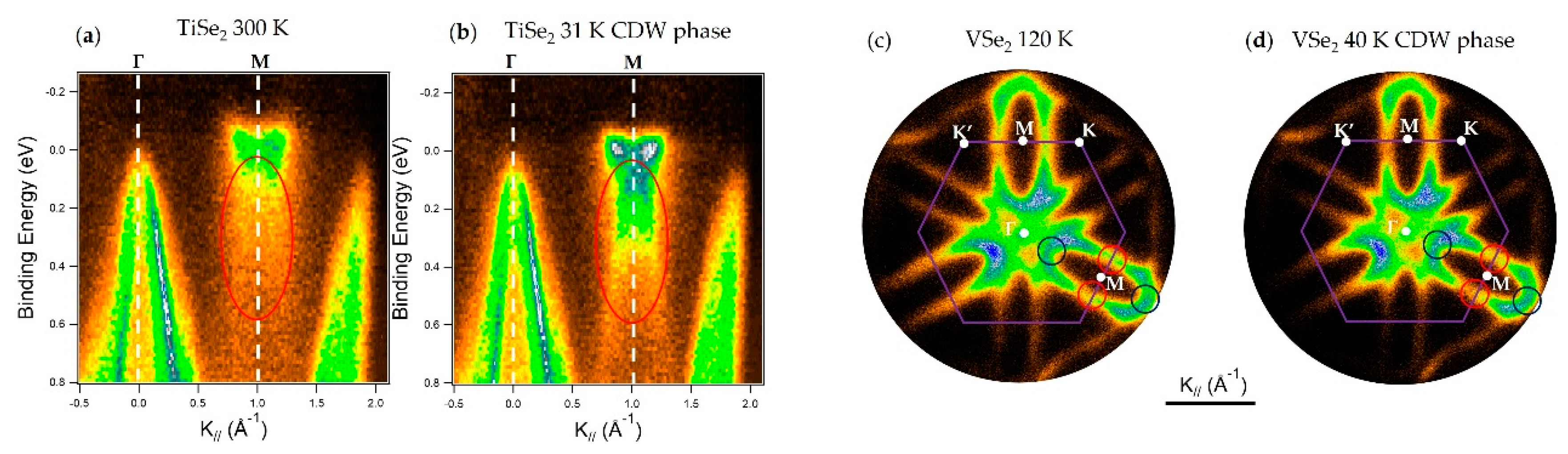
Figure 7.
ReS2 spatially resolved ARPES acquisitions. (a) Sketch of the exfoliated few-layer ReS2 sample; (b) Optical microscope image of the sample before transfer onto HOPG; (c) Real space PEEM image with Ebinding integrated over 30–50 eV (Re 5p/Re 4f core levels); (d) Second derivative k-space images selectively measured on the mono-layer and bi-layer areas of the sample with the surface BZ of ReS2 indicated in blue and of HOPG in orange. The high symmetry directions are marked by red lines; (e) Distorted 1T crystal structure of ReS2 with the Re chains forming along the b-axis of the crystal indicated in red. Adapted with permission from Ref. [11]. Copyright 2017 American Chemical Society. Nano-ARPES acquisition of bulk ReS2 (f) nano-ARPES signal (blue = low to orange = high) as a function of energy below the Fermi energy (vertical axis) and in-plane momentum k//, for excitation energies of 118 and 140 eV (left and right respectively); (g,h) panels show the nano-ARPES electronic dispersion of the valence bands at the Γ and Z points of the 3D Brillouin unit cell. Adapted with permission from Ref. [12]. Copyright 2017 Springer Nature.
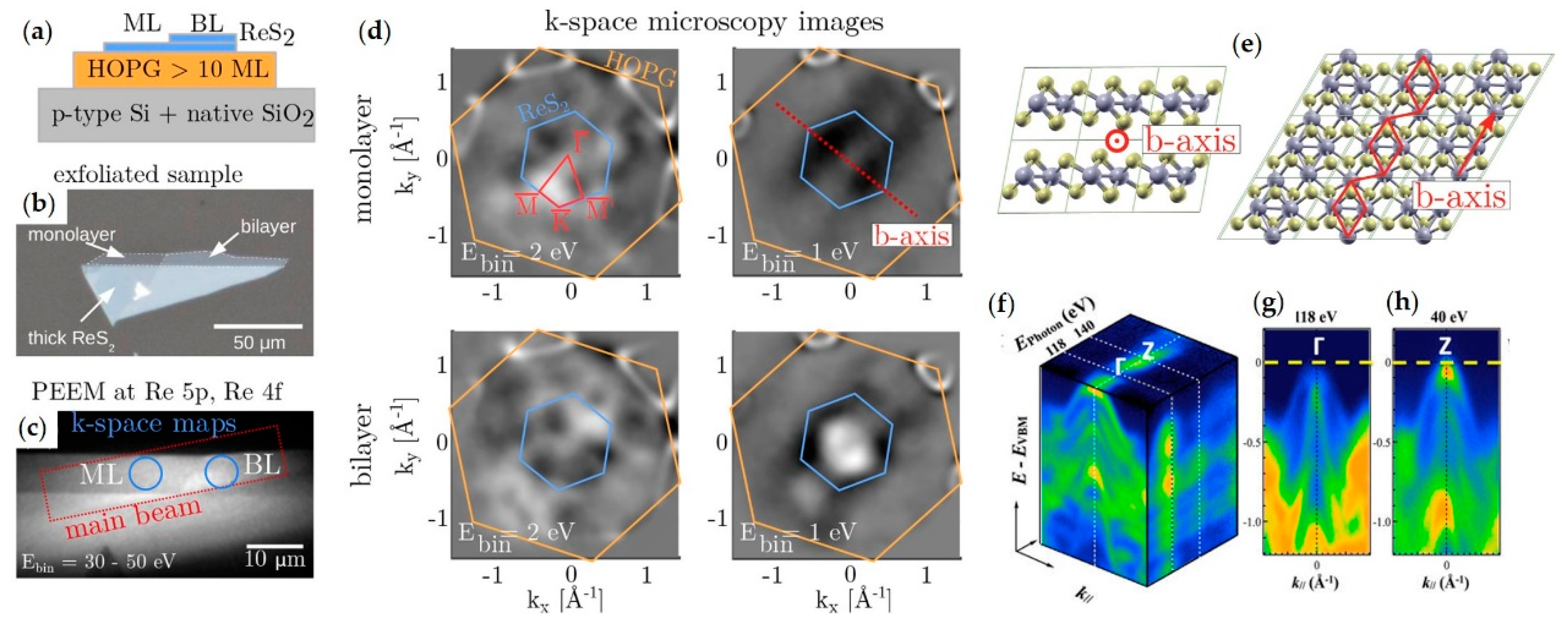
Figure 8.
Example of ARPES from graphene and TMDC heterostructure with gap opening. (a) Calculated band structure of MoS2 with the orbital character of the individual bands color-coded. Adapted with permission from Ref. [133] Copyright 2012 American Physical Society.; (b) 2nd derivative of E-k ARPES spectrum of graphene/MoS2 bulk. The observed band gaps in the graphene π-band are labeled and their respective position with respect to the MoS2 band structure are indicated in (a). Reprinted with permission from Ref. [13] Copyright 2015 American Chemical Society.

Figure 9.
Example of all-TMDC heterostructure study by means of ARPES, PEEM, and optical spectroscopy. (a) Optical image showing mono-layer MoSe2 and WSe2 sheets, which overlap, with the MoSe2 on top, in an aligned hetero-bi-layer region (H). Their boundaries are indicated with color-coded dotted lines; (b) Angle-integrated spectra in each of the three regions; (c) Map of the energy of maximum emission; (d–f) Momentum slices along Γ-K in the three regions, (top) unprocessed and (bottom) twice-differentiated, with cartoons of the structures above. The superposed dashed colored lines are DFT calculations for the MoSe2 mono-layer (green), the WSe2 mono-layer (red), and the commensurate hetero-bi-layer (blue). The white dashes in the lower panel of (f) indicate the VBM in the MoSe2 and WSe2 mono-layers and hence the valence band offset. The white dashed lines in the upper panels of (d–f) mark the VBM in the isolated MoSe2 (M) and WSe2 (W) mono-layers and in the aligned hetero-bi-layer (H). Adapted from [15]. Reprinted with permission from AAAS.


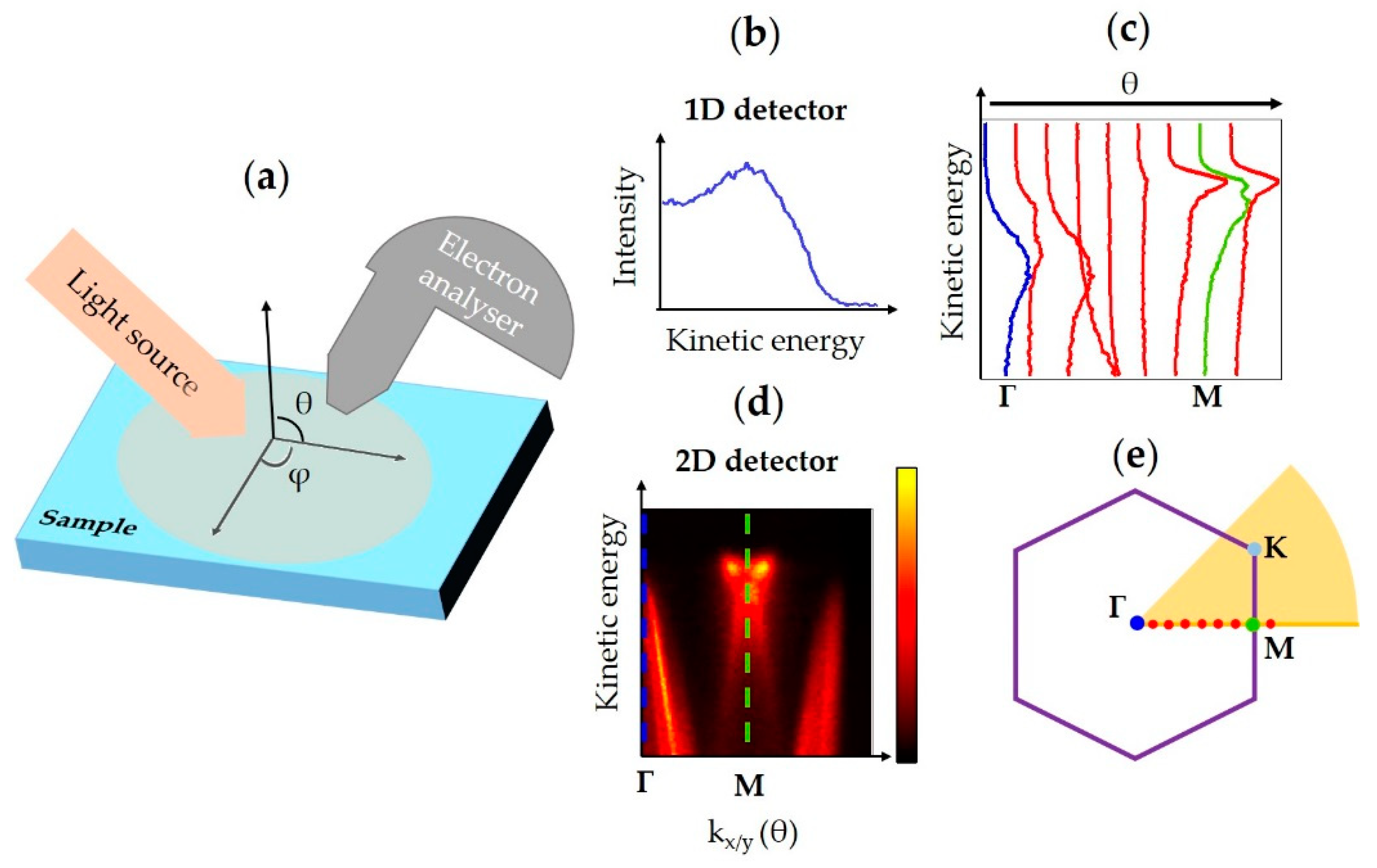
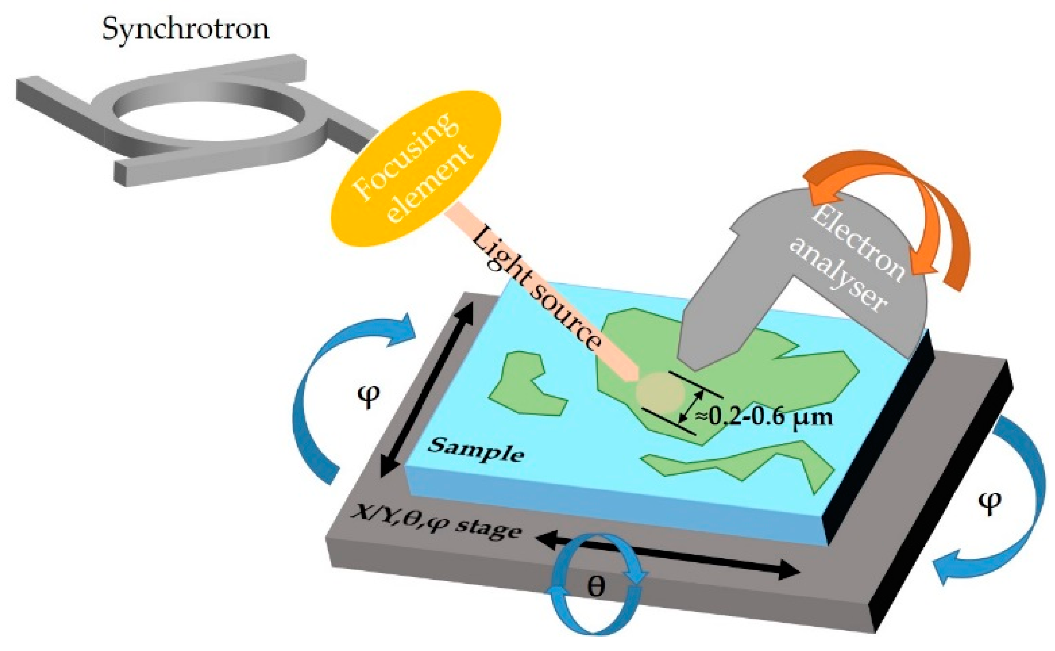
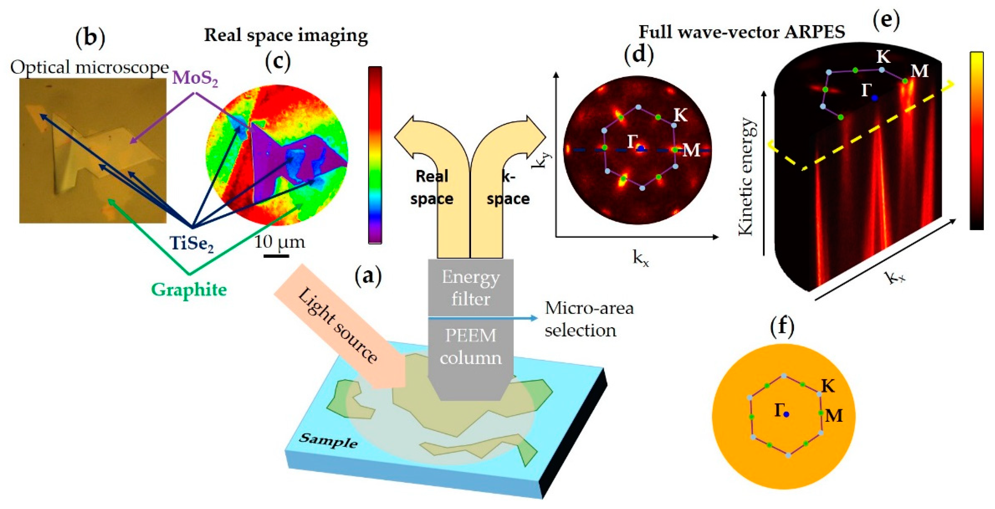
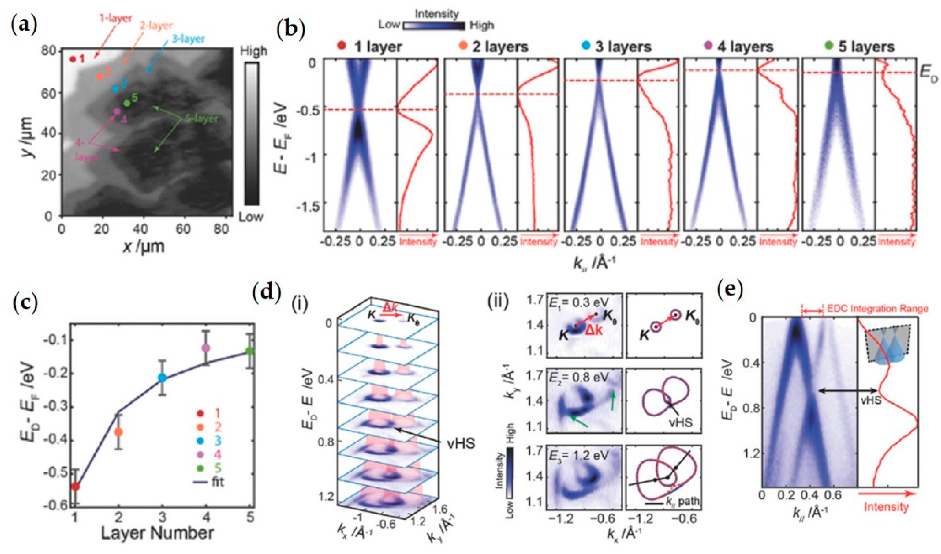
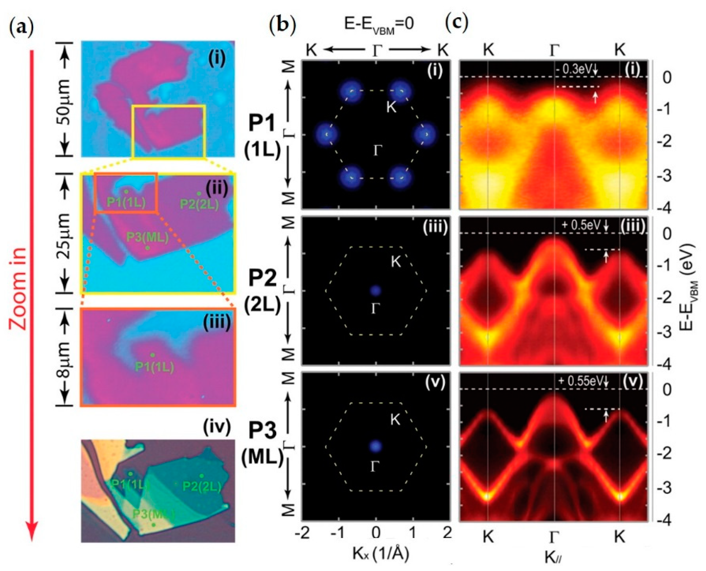
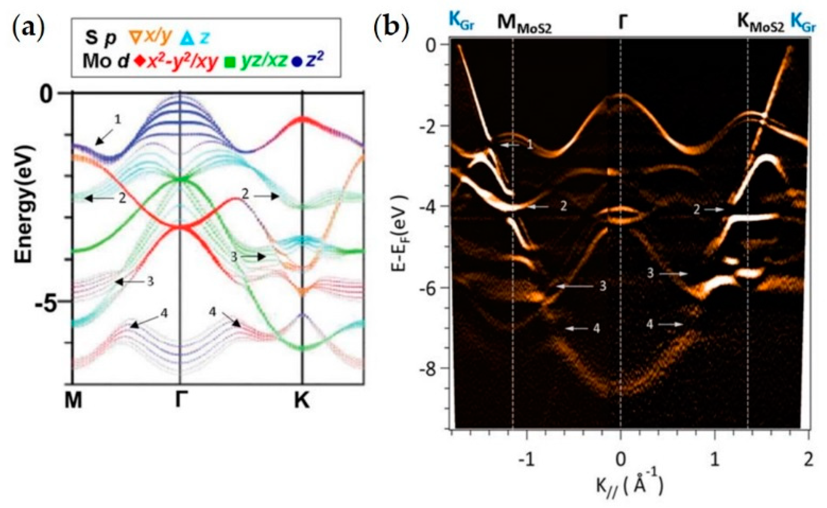
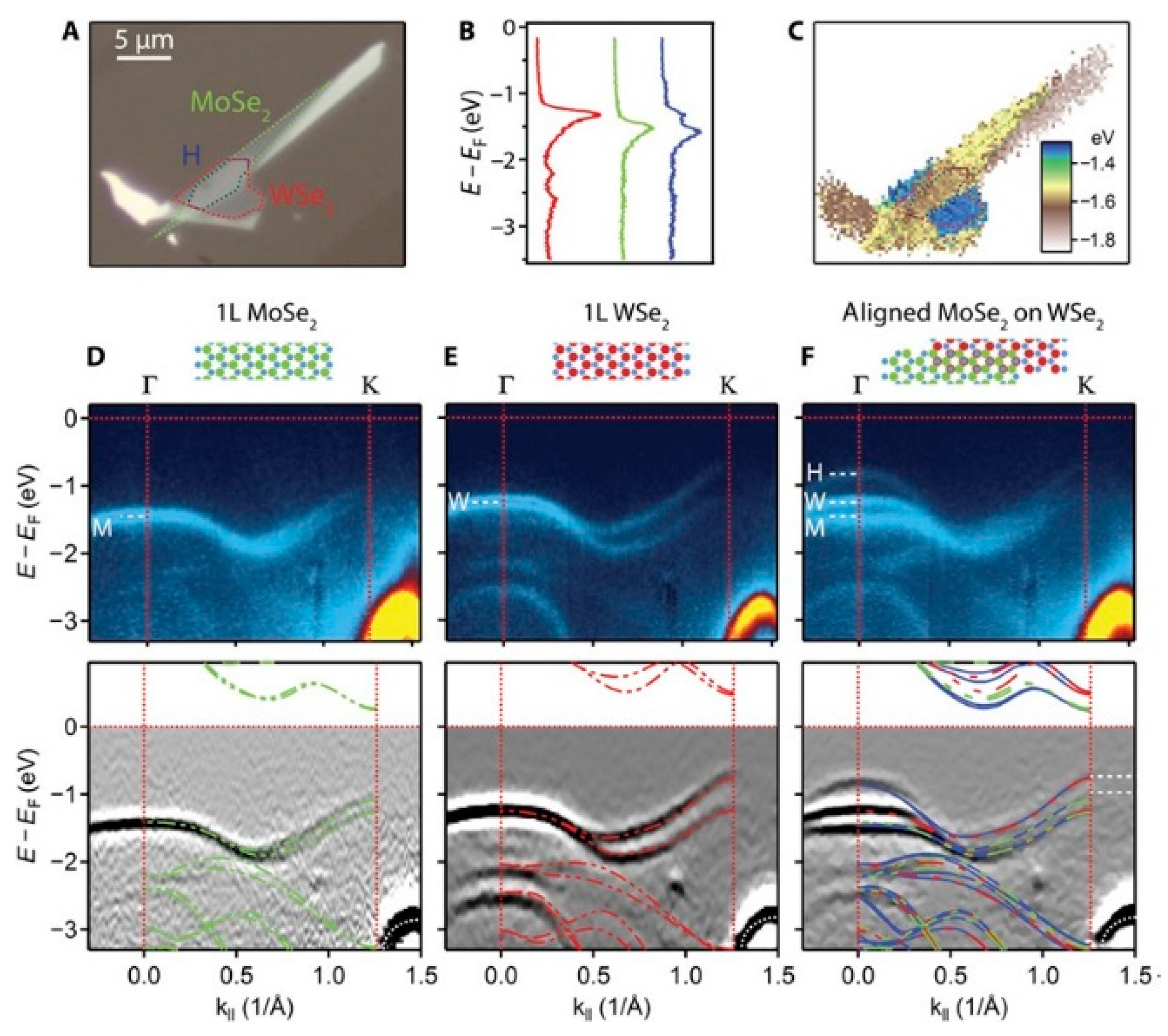
Table 1.
Different type of ARPES: advantages, disadvantages and future upgrades.
| Type of ARPES | Advantages | Disadvantages | Future Upgrades | |
|---|---|---|---|---|
| Conventional | Easy operation in laboratory and synchrotron facility. Best energy resolution for ARPES. | Requires large samples and several sample rotations. | Electron analyzers with deflectors can scan a sector of k-space without moving the sample. | |
| Spatially-resolved | Synchrotron beamlines | Strong light intensity, possibility to perform ARPES over tens of nanometers, photon versatility, kz sampling. | Requires: precise sample movements, rotations, access to specialized synchrotron beamlines. | Electron analyzers with deflectors can scan a sector of k-space without moving the sample. |
| EF-PEEM | Full-wavevector ARPES with no sample rotation or movement involved. These can be located in stand-alone laboratories with excellent stability. | Limited photon tunability, no kz sampling, lower signal intensity and larger sampling areas with respect to synchrotron nano-ARPES beamlines. | Time-resolved measurements by TOF PEEM, spin-resolved measurements with state-of-the-art detectors. | |
| Spin-resolved | ARPES with spin-resolution. | Intrinsic low signal, limited to large crystal or epitaxial films. | Integration of spin-sensitive detectors in EF-PEEM to perform full-wavevector ARPES and spatially-resolved measurements. | |
| Time-resolved | Studies of: charge carrier dynamics, band gap, empty states, time-dependent phenomena. | Low signal, limited to large crystal or epitaxial films. Complex lasers or time-resolved setups required as excitation sources. Space charge effects. | Advances in TOF PEEM setups and time-resolved light sources to perform spatial- and time-resolved studies. | |
© 2018 by the authors. Licensee MDPI, Basel, Switzerland. This article is an open access article distributed under the terms and conditions of the Creative Commons Attribution (CC BY) license (http://creativecommons.org/licenses/by/4.0/).
Share and Cite
MDPI and ACS Style
Cattelan, M.; Fox, N.A. A Perspective on the Application of Spatially Resolved ARPES for 2D Materials. Nanomaterials 2018, 8, 284. https://doi.org/10.3390/nano8050284
AMA Style
Cattelan M, Fox NA. A Perspective on the Application of Spatially Resolved ARPES for 2D Materials. Nanomaterials. 2018; 8(5):284. https://doi.org/10.3390/nano8050284
Chicago/Turabian StyleCattelan, Mattia, and Neil A. Fox. 2018. "A Perspective on the Application of Spatially Resolved ARPES for 2D Materials" Nanomaterials 8, no. 5: 284. https://doi.org/10.3390/nano8050284
Note that from the first issue of 2016, this journal uses article numbers instead of page numbers. See further details here.