Article

Measurements of Microstructural, Chemical, Optical, and Electrical Properties of Silicon-Oxygen-Nitrogen Films Prepared by Plasma-Enhanced Atomic Layer Deposition

1
State Key Laboratory of ASIC and System, Shanghai Institute of Intelligent Electronics & Systems, School of Microelectronics, Fudan University, Shanghai 200433, China
2
SMIT Center, School of Automation and Mechanical Engineering, Shanghai University, Shanghai 201800, China
3
A.N. Sevchenko Institute of Applied Physical Problems, Belarusian State University, 220045 Minsk, Belarus
*
Authors to whom correspondence should be addressed.
Nanomaterials 2018, 8(12), 1008; https://doi.org/10.3390/nano8121008
Submission received: 17 November 2018 / Revised: 1 December 2018 / Accepted: 3 December 2018 / Published: 5 December 2018

Abstract

:
In this study, silicon nitride (SiNx) thin films with different oxygen concentration (i.e., SiON film) were precisely deposited by plasma enhanced atomic layer deposition on Si (100) substrates. Thus, the effect of oxygen concentration on film properties is able to be comparatively studied and various valuable results are obtained. In detail, x-ray reflectivity, x-ray photoelectron spectroscopy, atomic force microscopy, and spectroscopic ellipsometry are used to systematically characterize the microstructural, optical, and electrical properties of SiON film. The experimental results indicate that the surface roughness increases from 0.13 to 0.2 nm as the oxygen concentration decreases. The refractive index of the SiON film reveals an increase from 1.55 to 1.86 with decreasing oxygen concentration. Accordingly, the band-gap energy of these films determined by oxygen 1s-peak analysis decreases from 6.2 to 4.8 eV. Moreover, the I-V tests demonstrate that the film exhibits lower leakage current and better insulation for higher oxygen concentration in film. These results indicate that oxygen affects microstructural, optical, and electrical properties of the prepared SiNx film.

1. Introduction

Silicon (Si)-based photonic components have received more and more attention recently. Their compatibility with conventional microelectronic device fabrication techniques and materials makes them attractive for potential applications in integrated optoelectronic technologies [1]. In the last decade, a variety of Si photonic components, such as optical modulators, optical waveguides, and optical detectors, have been successfully received [2]. However, silicon-based luminescent devices have not yet been achieved and still have a long way to go. Since the discovery of efficient photoluminescence in the red region in porous Si at room temperature [3], semiconductor nanoparticles have received much attention for their outstanding optical properties, especially, research on porous Si and Si nanoparticles indicates sustainable growth over the last decade [4,5,6]. In recent years, silicon nanocrystals (SiNCs) have roused significant attention on the applications of light sources [7] and “all-silicon” devices like silicon lasers, light-emitting diodes (LEDs), flash memories [8], tandem solar cells, and so on. The superlattice structure in a solid matrix allows to produce size-, density-, and shape-controlled SiNCs [9,10,11].
In recent years, a significant number of studies have been reported on SiNCs embedded in silicon dioxide (SiO2) and silicon nitride (Si3N4) [12,13]. In the case of SiNCs in SiO2, the correlation between the photoluminescence (PL) properties and the size of the nanocrystals has been discovered according to quantum confinement theory. However, because of the influence induced by the interface states between Si and SiO2 and the surface passivation of the nanocrystals with oxygen, the emission energy and luminescence intensity of SiNCs in silicon dioxide are limited [14,15,16]. Thus, buffering the silicon-rich silicon nitride (SRN) by an oxide layer has become an effective way to solve the problem [12]. Because of the excellent quality of the silicon nitride matrix [13], this method can in principle enhance the luminescence properties and ensure the quantum confinement effect [17,18,19].
Atomic layer deposition (ALD) is promising technology for advanced thin film deposition as it offers excellent control at the atomic scale over the thickness and uniformity of the film [20,21,22]. This allows the precise preparation of size- and distribution-controlled silicon nanocrystals. Thus, it will be a wonderful opportunity to fabricate silicon nitride and related superlattice by the ALD technique, and study its photoluminescence properties. Although there are many advantages of using the ALD technique in this area, there is still a lot of challenges that should be captured. First of all, most of the SiNCs and superlattices in previous studies are fabricated by CVD [23,24,25], sputtering [26,27,28], or other deposition techniques [29], there are few researches using ALD to fabricate superlattices. Besides, it is inevitable that there always exist oxygen defects or oxygen concentration in SiNx deposition. Therefore, preparing high quality silicon nitride film by ALD is one of the primary challenges.
There have been a certain number of studies on the growth of SiNx film using ALD [30,31,32], but rarely on its optical and electrical properties. Specifically, systematic study on the effect of oxygen contamination on photoelectrical properties of SiNx film is not present. Thus, in this study, plasma-enhanced atomic layer deposition was used to observe SiNx film with different content of oxygen by the purpose of studying the effect of oxygen on the physical, chemical, and photoelectrical properties of SiNx film (in other words this should be called SiON film). Specifically, basic film characteristics including microstructure, surface morphology, and roughness were evaluated. Then, attention was focused on the chemical bonding character of the obtained film, particularly the effect of oxygen content on the film’s chemical composition while the variation of binding energy was analyzed by Si 2p and O 1s in detail. Furthermore, optical properties like optical constant and energy band-gap of the SiON film with different oxygen content were determined by XPS measurements. At last, electrical properties of these SiON film were analysed to evaluate the effect of oxygen on electrical breakdown strength of these films and other electrical properties.

2. Experimental Section

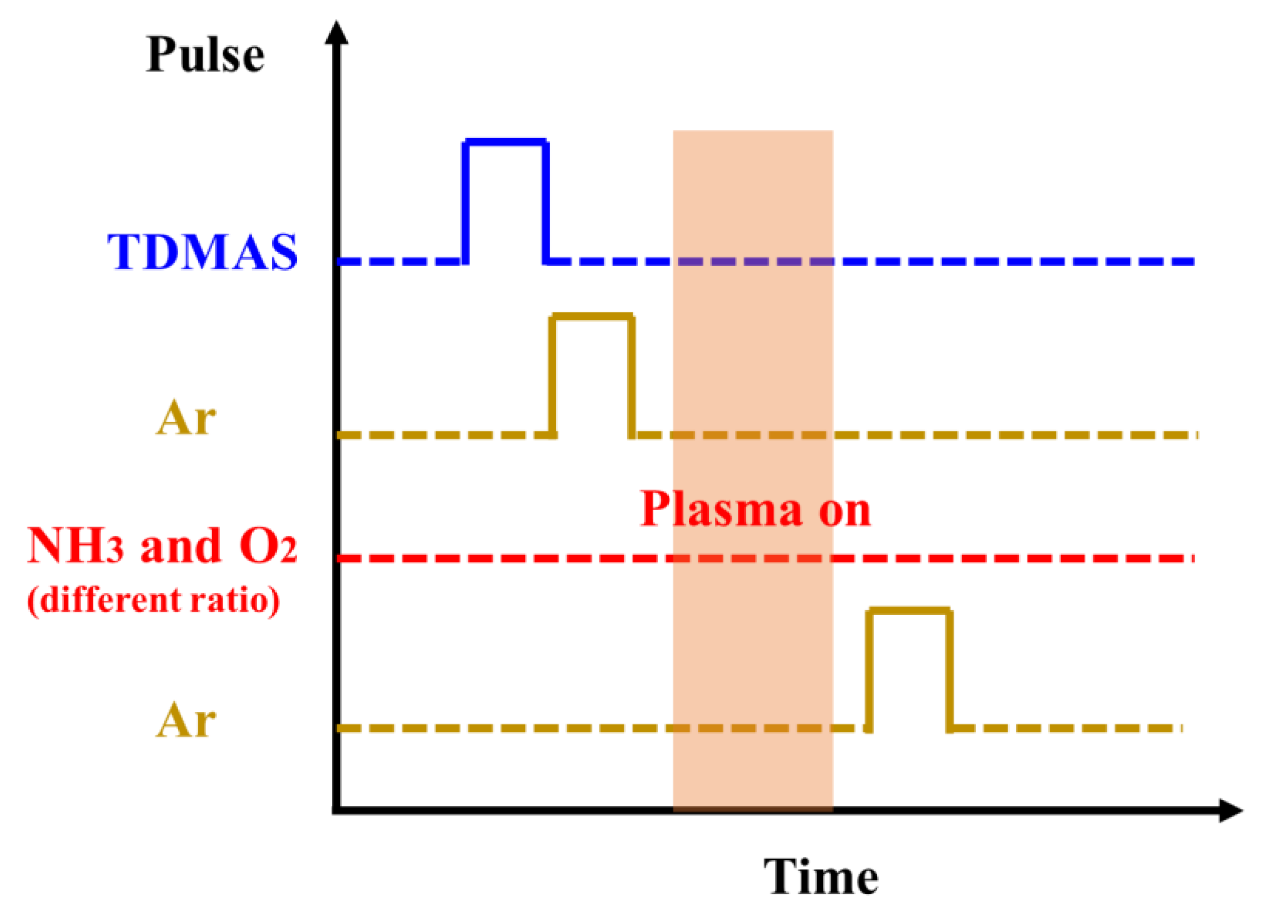
2.1. Preparation of SiON Film

SiON films with different oxygen concentration were sequentially deposited on p-type (1−10 Ω·cm) and p-type (0.01−1 Ω·cm) single polished Si(100) wafers in a BENEQ TFS200 ALD system (BENEQ, Finland) at 300 °C. The samples grown on p-type (0.01−1 Ω·cm) single polished Si(100) wafers were used to fabricate devices and measure electrical properties. Prior to deposition, the Si wafers were cleaned by a standard RCA process followed by a deionized water rinsing and drying in N2. During the deposition process, precursors for Si, N, and O were tris(dimethylamino)silane (TDMAS), N2 plasma, and O2 plasma, respectively. TDMAS was maintained at 20 °C in a stainless bottle. N2 and O2 plasma were activated at 200 W. The schematic diagram of one ALD cycle of SiON growth utilized in this work is shown in Figure 1. Each ALD cycle contains four steps: TDMAS pulse (2 s)/Ar purge (2 s)/plasma processing (10 s)/Ar purge (4s). In our experiment, different oxygen contents of SiON film are achieved by varying the flow of oxygen. It should be noted that the N2 and the O2 are simultaneously led into the chamber with different ratios in this work for realizing the direct growth of the SiON in one ALD cycle. At 300 °C, the O2 and the N2 react only with TDMAS when the plasma is turned on. As a result, the N2/O2 mixed gas is passed over the wafer continually during the deposition. For SiON-1 sample, the ratio of N2/O2 is 90:10, for SiON-2 sample, the ratio of N2/O2 is 95:5, then for SiON-3 sample, the ratio of N2/O2 is 99:1.

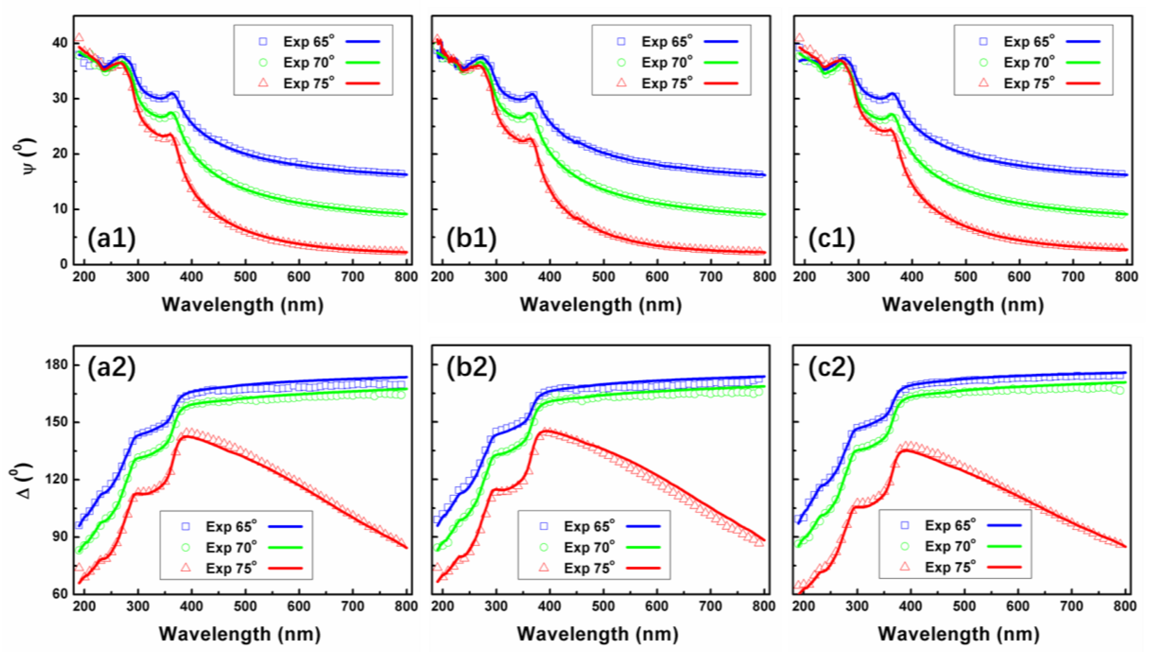
2.2. Sample Characterization

The microstructure and morphology of the films were characterized by X-ray reflection (XRR) (Bruker, D8, Billerica, MA, USA) and glow discharge optical emission spectroscopy (GDOES) (HIOKI, 200D, Nagano-ken, Japan). The surface morphology was observed using an atomic force microscope (AFM, Bruker, icon), and a typical 1 × 1 μm area was investigated using non-contact mode. SE measurements were performed on a rotating analyzer ellipsometer (SOPRA, GES-5E, Annecy, France). The incident angles were 65°, 70°, and 75°. The spectral wavelength range from 190 to 800 nm with a step of 2 nm, the system measured the spectra of Ψ and Δ as functions of wavelength (λ). The resulting spectra was fitted with WinElli_II software. The chemical bonding character of the obtained film was characterised by X-ray photoelectron spectroscopy (XPS) (SPECS, Berlin, Germany) using a monochromatic Al Kα source (hν = 1486.6 eV). A narrow scan resolution of 0.1 eV was used. The adventitious C 1s peak, arising from traces of hydrocarbon in the spectrometer, was used as a reference for evaluating the peak positions because of static charging of samples. The C 1s peak position was observed together with other peaks (Si 2p, N 1s, and O 1s) of the spectrum, and all the XPS spectra were calibrated by the C 1s peak at a binding energy of 284.6 eV.

3. Results and Discussion

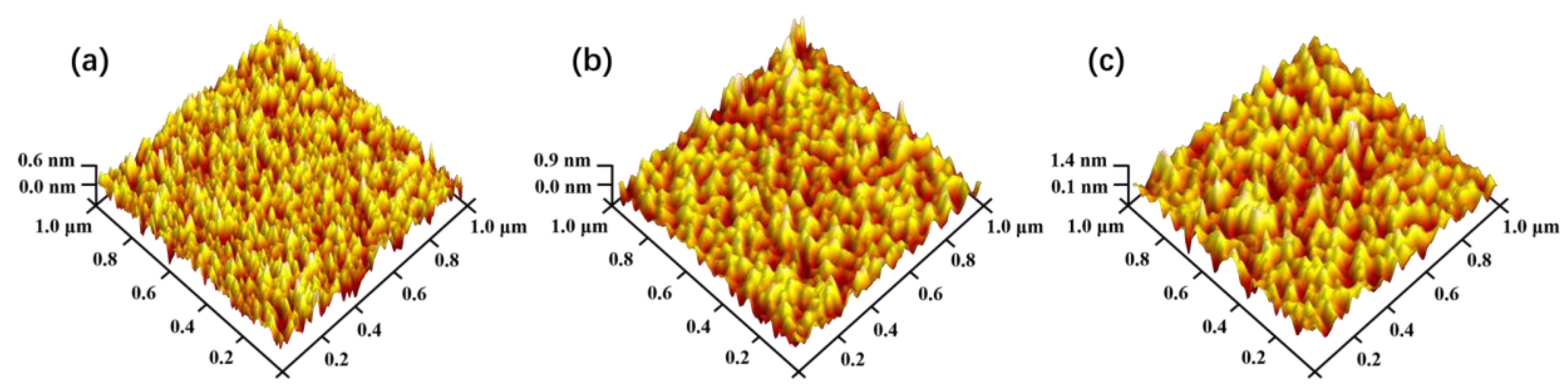
3.1. Surface Morphology and Microstructure

Figure 2a shows the measured and simulated XRR curve of the SiON film with different oxygen composition. The XRR spectra is simulated with a bilayer composed of a thin SiO2 buffer and the SiON film. The simple two-layer model fits very well with the data of all the films. The total external reflection angles of the SiON-1 sample is ~0.44°, it has a slight rise and becomes ~0.45° for the SiON-2 sample, then it increases to ~0.49°, revealing that the mass density of these three films increases, as shown in Figure 2b. The density of SiON-1 sample is 2.6 ± 0.1 g/cm3, with a slightly larger than the density of SiO2 (2. 2 ± 0.1 g/cm3), which means the film only contains such little part of nitrogen that it almost becomes a pure SiO2 film. Then, the mass density becomes 2.7 ± 0.1 g/cm3 for the SiON-2 film. Furthermore, the value of mass density goes on increases to 3.1 ± 0.1 g/cm3 for SiON-3 film. This is very close to the density of silicon nitride (3.2 g/cm3) [33], which means the SiON-3 film contains an insignificant part of oxygen concentration and the film is mainly consisted as silicon nitride.
The surface roughness obtained by XRR and AFM is shown in Figure 2c. The corresponding AFM mapping images of the films are shown in Figure 3. It is found that the surface roughness of all the films prepared in this work is very small, which means the film is very smooth. It should be noted here that both of XRR and AFM data present the similar trend of variation for roughness. Obviously, the RMS simulated from XRR data is almost two times higher than the value obtained by AFM, which is in agreement with the results reported in other work [34]. As see from the RMS values obtained by AFM, the SiON-3 film exhibits the highest RMS roughness value of about 0.2 nm, and the value of the other film is around 0.13–0.15 nm.

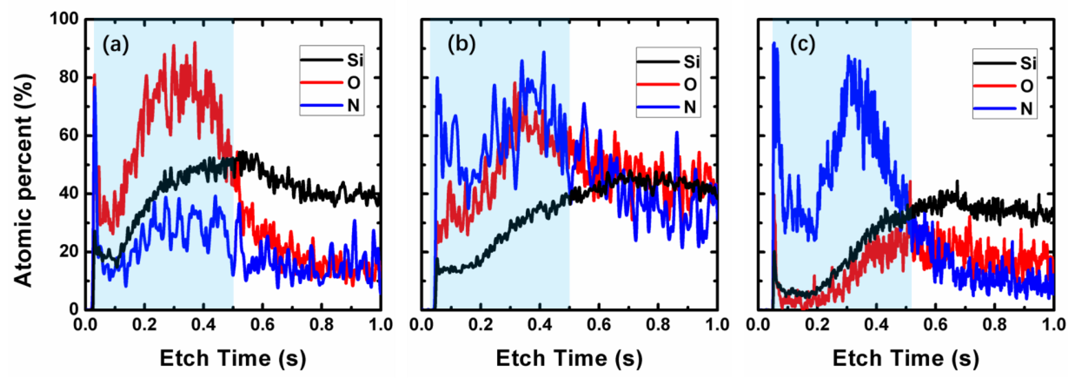
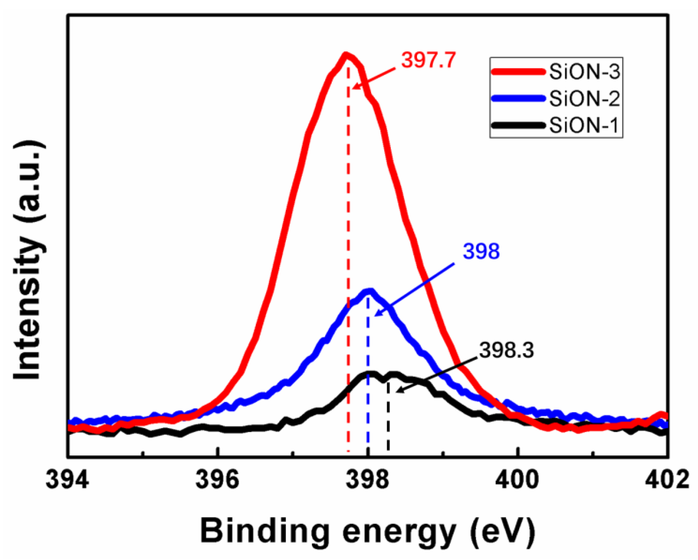
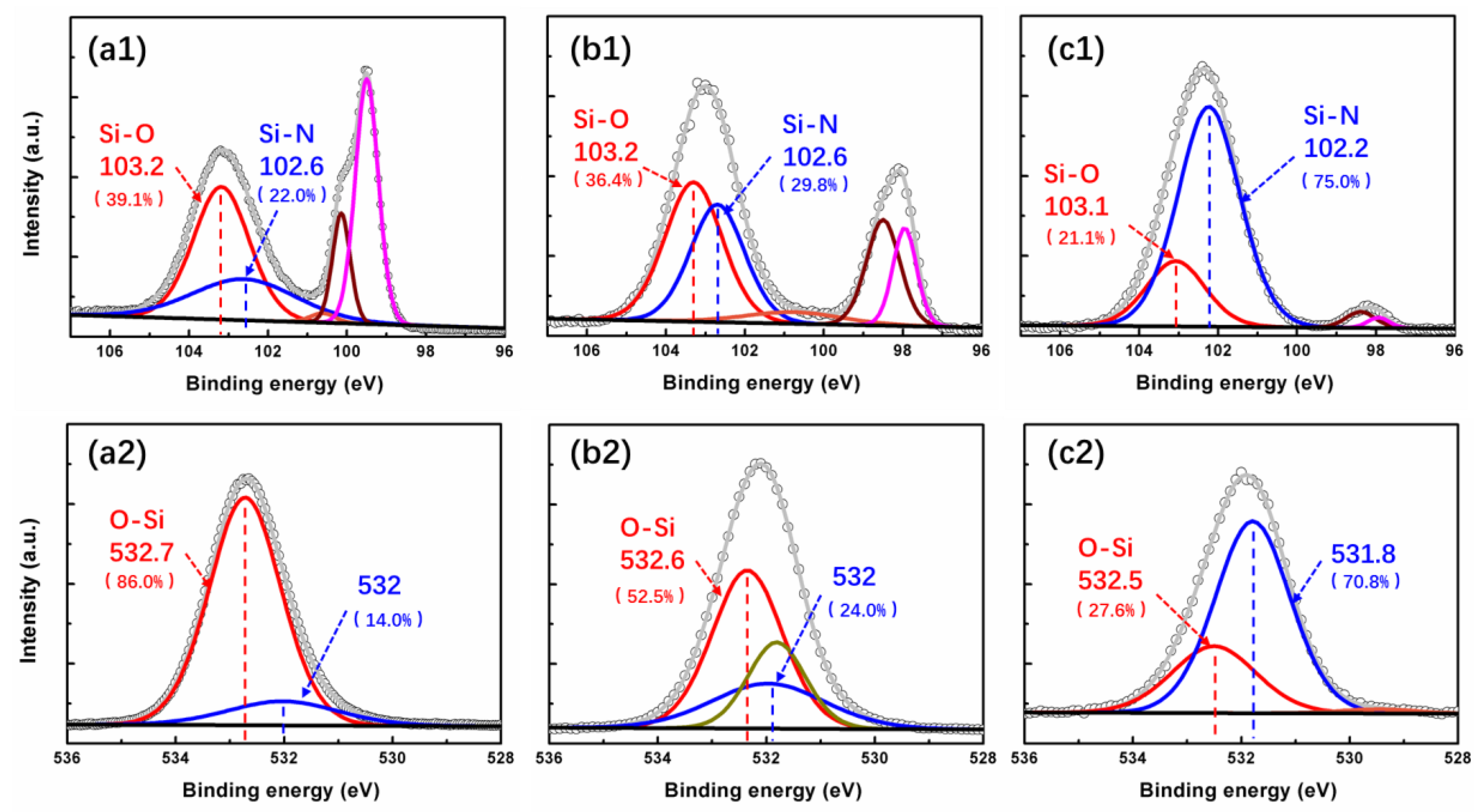
3.2. Content and Composition Analysis

To evaluate the distribution of Si, O, and N element in the entire film prepared in this work, all the samples were tested by GDOES firstly. Figure 4a–c show the GDOES depth profile of the SiON-1, SiON-2, and SiON-3 samples, respectively. The time needed for the etching of these three films is nearly the same, which means there little difference on the film thickness of these three samples. As shown in Figure 4, it is found that the average concentration of Si, O, and N element in the thin film (cyan region as be marked in Figure 4a–c) are all different for three samples. The concentration of oxygen is largest in SiON-1 sample but smallest in SiON-3 sample. However, the concentration of nitrogen presents completely the opposite variation tendency, which is smallest in SiON-1 sample but largest in SiON-3 sample. Then for SiON-2 sample, both of the oxygen and nitrogen concentration are kept medium. It is noteworthy that the variation trend of oxygen and nitrogen concentration in these samples verified the correctness of mass density obtained by XRR measurements.
X-ray photoelectron spectroscopy (XPS) was used to obtain detailed information about the elemental and chemical composition of the studied samples. Spectra of the as-prepared samples before the Ar+ ion bombardment contained only the characteristic peaks of photoelectrons created by the ionization of the inner electron shells of silicon (Si 2p) and oxygen (O 1s) atoms composing the SiO2 protective layer. To establish the composition of the SiON-1, SiON-2, and SiON-3 film under study, we applied the Ar+ ion treatment of the sample surface necessary for the removal of possible contamination and for etching of the protective SiO2 layer. Figure 5 displays the photoelectron spectra of the studied film in the energy region of N 1s levels. It can be seen clearly that the intensity of N1s peaks for SiON-1 film is weakest, SiON-2 film comes second, and SiON-3 film has the largest N 1s peak. This result means the content of nitrogen for SiON-3 film is much larger than SiON-1 and SiON-2 film. Besides, for SiON-1 film, the peak location of the N 1s is 398.3 eV, the value changed to 398 eV for SiON-2 film, and then it turned into 397.7 eV for SiON-3 film. From the variation of the location of N 1s peak, it can be found that the N 1s peak shifted toward higher energy when the content of oxygen increased in the SiON film. This can be explained by the redistribution of the electron density owing to the presence of oxygen in silicon oxynitride layers and by the presence of the contribution from the N–O bonds (e.g., (Si-)2 N–O with an energy of about 399.7 eV [35]).
To further analyze the concentration, microstructure, chemical valence, and composition of the film and elements, the Si 2p and O 1s spectra of the SiON sample are examined by high-resolution XPS, as shown in Figure 6. From the Si 2p spectrum of the SiON-1 film (Figure 6a1), five peaks are observed at 103.2, 102.6, 100.6, 100.1, and 99.5 eV, corresponding to the Si–O (SiO2), Si–N (Si3N4), Si–N (SiNx), Si–Si (Si 2p 3/2), and Si–Si (Si 2p 1/2) bonds [36,37,38], respectively. The intensity and area of the Si–O related subpeak is larger than the Si–N ones, this result declared the SiON-1 film contains more content of oxygen than nitrogen. For the SiON-2 sample, three subpeaks centered at 103.3, 102.2, and 100.8 eV are observed except for the Si substrate. They are assigned to be the Si–O (SiO2), Si–N (Si3N4), and Si–N (SiNx) bonds, respectively. It is worth to point out that the intensity and area of the Si-N related subpeak increased compared with the strength in SiON-1 sample, which means the content of nitrogen increased in SiON-2 film. For SiON-3 sample, only two subpeaks centered at 103.2 and 102.2 eV are observed except for the Si substrate. They are assigned to be the Si–O (SiO2) and Si–N (Si3N4) bonds, respectively. It can be observed that the Si 2p spectra of the SiON-3 sample is dominated by the Si–N bonds. The existence of the Si–O bonds is ascribed to the oxidation effect after the Si3N4 film is exposed to the atmosphere. The other part of the Si–O bonds comes from the residual oxygen inside the film. By comparison of the O 1s spectra of SiON-1 (Figure 6a2) and SiON-2 samples (Figure 6b2) with that of the SiON-3 sample (Figure 6c2), more accurate bonding state information on the oxygen inside the SiON film can be achieved. All three films can be fitted mainly by two subpeaks located at ~532.6 and ~532 eV, corresponding to O–Si (bulk) and O–Si–N bonds, respectively [39]. For the O 1s spectra of the SiON sample, the existence of the O–Si bonds (Figure 6a2) corresponds with the Si–O bonds of the matching sample found in Si 2p (Figure 6a1). Moreover, the existence of the O–Si–N bonds confirms the formation of a ternary compound of SiOxNy in the SiON sample. It reveals that the prepared SiON sample is not a “mixture” of Si3N4 and SiO2. Normally, ALD growth of ternary compound is realized by alternately growing two kinds of binary compounds.
As the content of nitrogen plasma increasing from 95% to 99%, XPS intensity of the subpeak related to Si–O (SiO2) bonds decreases, while the subpeak centered around 532 eV (531.8 eV) increases. The variation of the intensity ratio of two subpeaks related to O–Si bonds indicates that the concentration of the oxygen decreases with the increasing of nitrogen plasma. The change of the O 1s and the Si 2p both implied that less Si–O bonds is present when increasing the nitrogen plasma, which agree with the previous researchers [35,36,37]. Besides, as seen in Figure 6, a small increase of the binding energy for Si–O, Si–N, and O–Si bonds is observed as increasing oxygen concentration. This small shift presents the same variation tendency with N 1s in Figure 5. It is well known that elements exhibit binding energy peaks, and their relative position depends on the electronegativity of surrounding atomic neighbors. Then, in the case of a phase mixture when more than one bonding state exists, a particular element is expected to have various binding energies, caused by different coordination/neighbors [36]. Therefore, the slight changes of binding energy for these chemical bonds in this study may also induced by the presence of oxygen in silicon oxynitride layers, and by the contribution from the O–N, Si–O–N, or other related bonds [35].

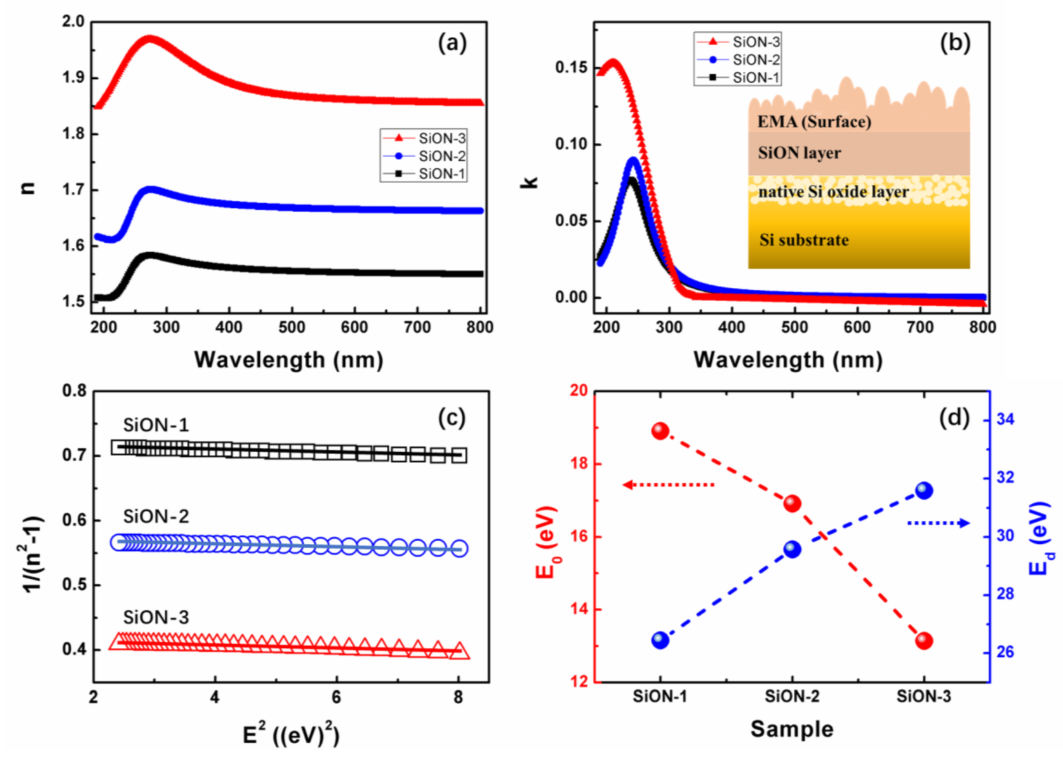
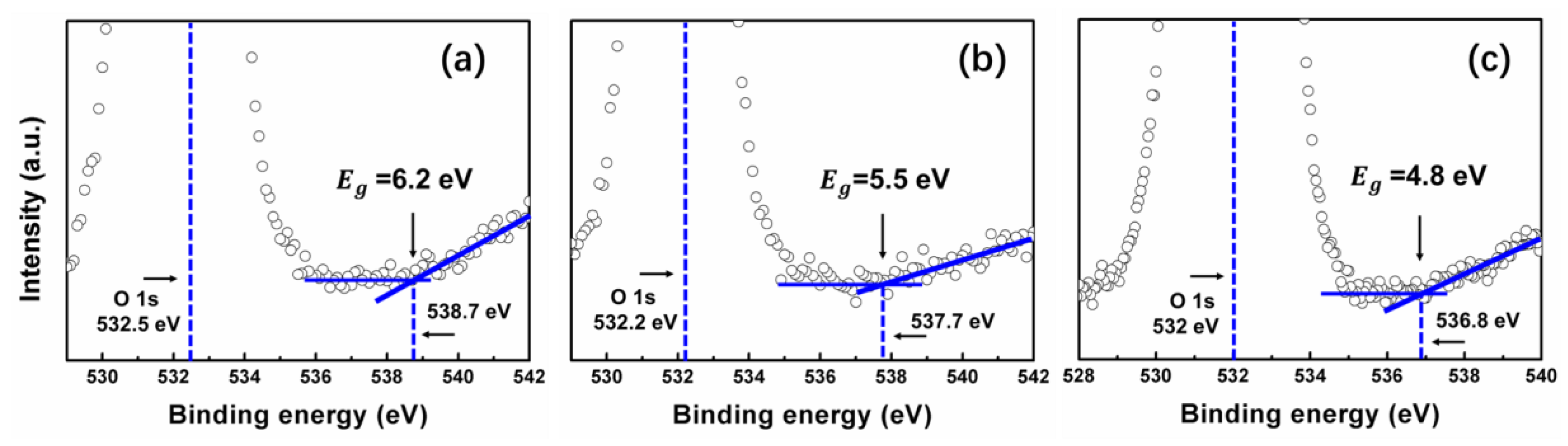
3.3. Optical Properties

In order to achieve in-depth knowledge on the evolution of the optical properties, variable angle (65°, 70°, and 75°) spectroscopic ellipsometry measurements have been performed on SiON film. The sample model used to analyze the raw ellipsometry data consists of (i) a semi-infinite crystalline silicon substrate, (ii) a native silicon dioxide layer, (iii) a homogenous, isotropic layer representing the SiON layer, (iv) surface roughness, and (v) air as the ambient medium. The top layer was described by an effective medium approximation (EMA) following the Bruggeman law [40] presents the surface roughness as a mix of the optical response of vacuum and SiO2 in a 50–50% concentration. The dielectric function of the SiON layer is modeled by the Tauc-Lorentz (T-L) oscillator model. The complex dielectric function of the energy (E) is defined as ε ( E ) = ε 1 + i ε 2 . In the T-L model, ε 1 and ε 2 are defined as [41,42]:
ε 2 = [ A E 0 C ( E E g ) 2 ( E 2 E 0 2 ) 2 + C 2 E 2 × 1 E ] ,   E > E g , ε 2 = 0 ,   E < E g ,
and
  ε 1 = ε 1 ( ) + 2 π P E g ξ ε 2 ( ξ ) ξ 2 E 2 d ξ
where A, E0, C, and Eg represents the amplitude, peak transition energy, broadening term, and band-gap of the oscillator, respectively, all using units of energy (eV). For ε 1 , ε 1 ( ) is a fitting constant to prevent ε 1 from converging to zero for energies below the band-gap, and P stands for the Cauchy principal part of the integral [42].
SE measurements are performed at room temperature immediately after removing the samples from the deposition system to avoid surface contamination. The measured and simulated Ψ and Δ of SiON thin films for angles of incidence of 65°, 70°, and 75° are shown in Figure 7. The degree of fitting are all above 99% in the desired wavelength range (190–800 nm). As shown in Figure 7, the simulated data (solid line) are indistinguishable from the measured data (scatter line), indicating that the structure of the optical oscillator model used is unique below, through, and above the bandgap energy (i.e., UV–VIS–NIR). A remarkable fact in this figure is that both of Ψ and Δ for each sample decreased with increasing angles of incidence from 65° to 75° gradually. This difference could be related to the altered microstructure (surface morphology, roughness, and density) seen for these samples (Figure 2 and Figure 3) and points to the fundamental role this characteristic could play in the optical behavior of nanostructured SiON layers.
Basing on the above theory, the optical constants of SiON thin film are extracted and obtained from the fitted Ψ and Δ. Figure 6a shows the changes of the refractive index (n) as a function of wavelength in the range of 190–800 nm. Evidently, SiON-1 film exhibits the lowest n value of 1.55 at 632.8 nm, while the SiON-3 film exhibits a highest n value of 1.86 at 632.8 nm. Obviously, the refractive index decreases monotonously when oxygen content increases. It is well know that SiO2 film presents a low refractive index of about 1.4. As the oxygen content in SiON film increases, the ratio of SiO2 in the multilayer mixed with SiNx, SiO2, and other constituents will increase gradually, which, to some extent, induces the decrease of the refractive index of SiON. Figure 8b describes the extinction coefficient k of these three films. The inset presents the structure that is used to describe the SiON samples and model the ellipsometry data. The k value of all films is close to zero infinitely in the wavelength range of 400–800 nm, which indicates that the films are nearly transparent in this wavelength region [43]. Moreover, a red shift of the absorption edge can be observed with decreasing oxygen composition in SiON film, which is supposed to result from the variation of band-gap among these films, which will be discussed later. Therefore, the refractive index and the extinction coefficient of the SiON film can be effected by varying the oxygen concentration.
The refractive index dispersion n of SiON film was further fitted by the Wemple-DiDomenico model [44]. Then, the effect of oxygen concentration on the refractive index dispersion data in the spectra below the band-gap (1.55 eV < E < 2.8 eV) was investigated. The refractive index data can be fitted in this spectral range to the single oscillator expression [45]:
n 2 = 1 + E 0 · E d E 0 2 E 2  
where E represents the photon energy, E0 is the oscillator energy, and Ed is called dispersion energy, which measures the oscillator strength (the strength of interband optical transitions). From linear regression of dependence (n2 − 1)−1 against E2 (as shown in Figure 8c), the parameters E0 and Ed can be calculated.
Figure 8d displays the variation of E0 and Ed of different SiON film. For SiON-1 sample, E0 is ~19 eV and Ed is ~26 eV. For SiON-2 sample, E0 is ~17 eV and Ed is ~30eV. Then, for SiON-3 sample, E0 is ~13 eV and Ed is ~32 eV. For the dispersion energy, an empirical relation is established [45]: Ed = βNcNeZa, where β is a constant, according to Wemple, β has a value of 0.37~0.04 eV. Nc is the coordination number of the nearest neighboring cation to the anion, and Za is the formal chemical valency of the anion, then Ne is the total number of valence electrons per anion [46]. For Si3N4, Ne = [(4 valence electrons)·(3 silicon cation) + (3 valence electrons)·(4 oxygen anions)]/4 = 6 and Za = 3. For SiO2, Ne = [(4 valence electrons)·(1 silicon cation) + (6 valence electrons)·(2 oxygen anions)]/2 = 8, and Za = 2. Thus, Nc can be calculated from the relationship: Nc = Ed/βNe Za. for SiON-1 sample, Nc ranges from 3.6 to 4.1, and it becomes 4.1 to 4.6 for SiON-2 sample, then for SiON-3 sample, it ranges from 4.3 to 4.9. From the variation trend of Ed and Nc, it is found that the values of these two parameters increase with the decrease of oxygen concentration in SiON film. So, it can be concluded that SiON-1 film has a more amorphous structure than SiON-3 film. This result correlates with the fact that the film with more oxygen defects is less dense and have a lower refractive index [47]. Evidently, Figure 2b and Figure 8a demonstrate that the variation of film density and refractive index agree with the variation of Ed and Nc perfectly. Furthermore, the increase of Ed from SiON-1 to SiON-3 sample is also supposed to relate to the effective number of valence electrons, the variation of Si-N, Si-O, and Si-Si bonds, as shown in Figure 6.
Moreover, the long-wavelength limit of the refractive index, n(0), is given by [47]: n2(0) = 1+ Ed/E0. Then n(0) is calculated to be 1.55, 1.66, and 1.85 for SiON-1, SiON-2, and SiON-3, respectively. These simulated results are in excellent agreement with the refractive index in Figure 8a, which improved the correctness of the model.
It is important to determine the optical band-gap energy (Eg) of a thin film material, because Eg is usually essential to develop the electronic band structure of a material, besides, Eg also effects the application of a film in the field of optoelectronic devices. Thus, we calculated the Eg of these SiON films. Figure 9 shows the determination of the Eg of the ALD SiON thin film using XPS O1s data. The method using the energy-loss peak of the O 1s spectrum to determine the Eg value of large band-gap materials has been reported by numerous scientists [48,49,50]. Thus, a representative high-resolution scan of the O 1s core level of SiON-1, SiON-2, and SiON-3 film obtained in this work are shown in Figure 9a–c. We can notice that the Eg is 6.2, 5.5, and 4.8 eV for SiON-1, SiON-2, and SiON-3 film, respectively. Which indicates that the optical band-gap energy of SiON films decreases with decreasing oxygen composition.

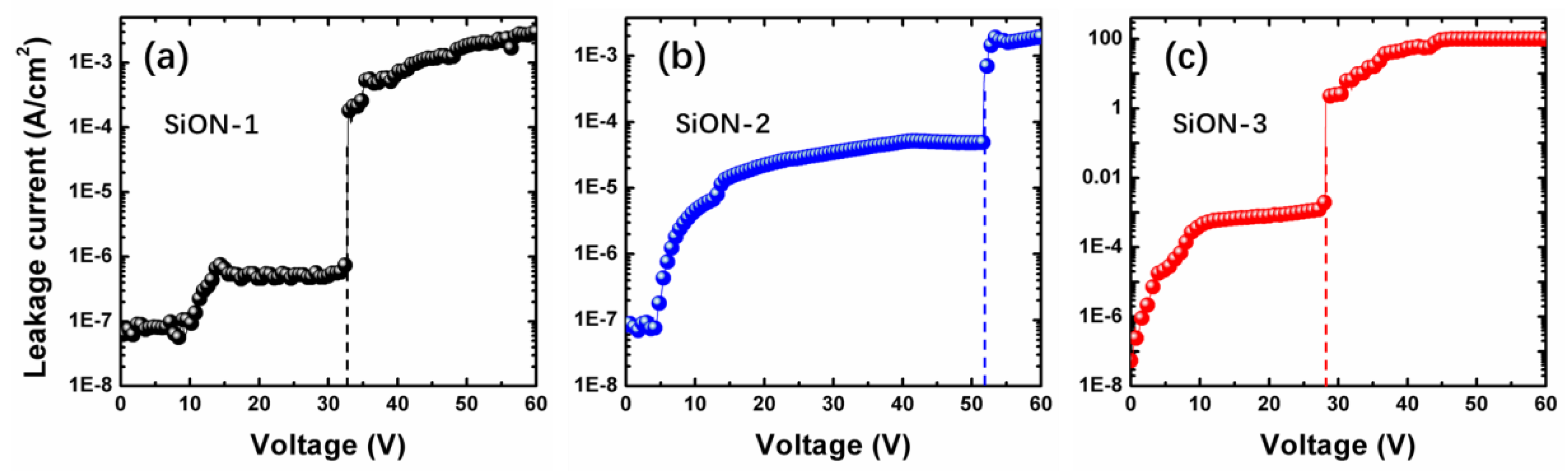
3.4. Electrical Properties

To examine the reliability of SiON film prepared in this work, J−V tests were performed on the prepared samples. The Cr/Au top electrodes (with a thickness of 200 nm and 50–300 μm in width square shape arrays) were deposited on the samples. As shown in Figure 10, all of the three samples exhibit no visible “soft” breakdown (lead by the defects in the dielectric film) point until the final “hard” (intrinsic) breakdown point is reached. This indicates that there are no obvious pinholes or cracks inside the dielectric film. Besides, the leakage current of all samples is about 1 × 10⁻⁷ A/cm2 at 1 V. For SiON-1 film, the leakage current keep at 1 × 10⁻⁷ A/cm2 until the voltage increases to 10 V. For SiON-2 film, the leakage current fluctuates around 1 × 10⁻⁷ A/cm2 until the voltage increases to 5 V. However, for SiON-3 film, the leakage current has a sharp increase at the very beginning when the voltage increases from 0 V to 5 V. These results suggest that the insulation characteristics of these three samples exhibit a big difference. In addition, we found the film presents lower leakage current and better insulativity with increasing oxygen concentration in SiON film, which makes it more suitable for dielectric and passivation materials [51]. As reported by many previous studies, the electrical insulation of SiO2 film is better than Si3N4 film [52,53]. It is suggested the SiON-1 sample with largest oxygen content has the best electrical insulation compared to other samples. As seen in Figure 10, the breakdown voltage is 33 V and 28 V for SiON-1 and SiON-3 film. However, the one for SiON-2 film is around 52 V, which is obviously much higher than other two samples. It is suggested that the breakdown field of SiON-2 sample is highest as the thickness of all three samples are kept the same (~15 nm). This result presents familiar tendency with AlON film in previous article [34], in which the AlON film shows higher breakdown field than both of Al2O3 and AlN film. The possible reason is that the nitrogen concentration in the SiON (AlON) film is beneficial for relieving the interfacial strain at the Si/SiON (Si/AlON) interface [54]. On the basis of this finding, the different characteristics of SiON film with different oxygen concentration can be utilized to fabricate high-performance electrical devices with desired properties.

4. Conclusions

In this study, high quality nano-scale SiON thin film was successfully deposited by using PEALD. The precursors of N2 and O2 are simultaneously introduced into the chamber during film growth at a temperature of 300 °C. It is believed that the composition of the obtained film quickly changes from SiNx to SiO2 when a small amount of O2 is introduced into the chamber. From various measurements of SiON film with different oxygen concentration, the effects of oxygen concentration on properties of SiON film are systematically studied. It is found that the refractive index of SiON film increases from ~1.55 to ~1.86 as oxygen content decreases, while the surface roughness increases from 0.13 nm to 0.2 nm. Furthermore, the energy band-gap of SiON film decreases from ~6.2 eV to ~4.8 eV as the oxygen concentration in the film reduces. Regarding the electrical aspect, the MOS capacitor with SiON dielectric shows different electrical properties, the leakage current of SiON film appears inversely proportional to the oxygen concentration, and the SiON film with medium oxygen concentration presents much higher breakdown voltage than the other films. These results indicate that the oxygen concentration has an obvious influence on the microstructural, optical, and electrical properties of SiON film. In addition, various findings in this work inspire us to explore for further applications of SiON film in optoelectronic devices.

Author Contributions

Conceptualization, H.-P.M. and H.-L.L.; Data curation, H.-P.M., T.W., W.H. and G.-J.Y.; Formal analysis, J.-H.Y. and X.-X.L.; Investigation, H.-P.M.; Project administration, H.-L.L. and F.F.K.; Supervision, H.-L.L. and D.W.Z., H.-P.M. wrote the paper.

Funding

This research was funded by the National Key R&D Program of China (No. 2016YFE0110700), National Natural Science Foundation of China (No. U1632121, 11804055, 51861135105 and 61874034), and China Postdoctoral Science Foundation (No. 2018M631997).

Acknowledgments

The authors want to thank Pei-Hong Cheng from ShanghaiTech University for her great help during XPS measurements.

Conflicts of Interest

The authors declare no conflict of interest.

References

  1. Zhigunov, D.M.; Sarikov, A.; Chesnokov, Y.M.; Vasiliev, A.L.; Zakharov, N.; Kashkarov, P.K. Thickness and temperature depending intermixing of SiOx/SiO2 and SiOxNy/SiO2 superlattices: Experimental observation and thermodynamic modeling. Appl. Phys. Lett. 2016, 108, 223102. [Google Scholar] [CrossRef]
  2. Wang, D.-C.; Zhang, C.; Zeng, P.; Zhou, W.-J.; Ma, L.; Wang, H.-T.; Zhou, Z.-Q.; Hu, F.; Zhang, S.-Y.; Lu, M.; et al. An all-silicon laser based on silicon nanocrystals with high optical gains. Sci. Bull. 2018, 63, 75–77. [Google Scholar] [CrossRef]
  3. Canham, L.T. Silicon quantum wire array fabrication by electrochemical and chemical dissolution of wafers. Appl. Phys. Lett. 1990, 57, 1046–1048. [Google Scholar] [CrossRef]
  4. Kanemitsu, Y. Luminescence properties of nanometer-sized Si crystallites: Core and surface states. Phys. Rev. B 1994, 49, 16845–16848. [Google Scholar] [CrossRef]
  5. Ghislotti, G.; Nielsen, B.; Asoka-Kumar, P.; Lynn, K.G.; Gambhir, A.; Di Mauro, L.F.; Bottani, C.E. Effect of different preparation conditions on light emission from silicon implanted SiO2 layers. J. Appl. Phys. 1996, 79, 8660–8663. [Google Scholar] [CrossRef]
  6. Chen, L.-Y.; Chen, W.-H.; Hong, F.C.-N. Visible electroluminescence from silicon nanocrystals embedded in amorphous silicon nitride matrix. Appl. Phys. Lett. 2005, 86, 193506. [Google Scholar] [CrossRef]
  7. Pavesi, L.; Dal Negro, L.; Mazzoleni, C.; Franzo, G.; Priolo, F. Optical gain in silicon nanocrystals. Nature 2000, 408, 440–444. [Google Scholar] [CrossRef]
  8. Tiwari, S.; Rana, F.; Hanafi, H.; Hartstein, A.; Crabbé, E.F.; Chan, K. A silicon nanocrystals based memory. Appl. Phys. Lett. 1996, 68, 1377–1379. [Google Scholar] [CrossRef]
  9. Zacharias, M.; Heitmann, J.; Scholz, R.; Kahler, U.; Schmidt, M.; Bläsing, J. Size-controlled highly luminescent silicon nanocrystals: A SiO/SiO2 superlattice approach. Appl. Phys. Lett. 2002, 80, 661–663. [Google Scholar] [CrossRef]
  10. Gutsch, S.; Hiller, D.; Laube, J.; Zacharias, M.; Kubel, C. Observing the morphology of single-layered embedded silicon nanocrystals by using temperature-stable TEM membranes. Beilstein J. Nanotechnol. 2015, 6, 964–970. [Google Scholar] [CrossRef] [Green Version]
  11. Yi, L.; Scholz, R.; Zacharias, M. Size and density control of Si-nanocrystals realized by SiOx/SiO2 superlattice. J. Lumin. 2007, 122–123, 750–752. [Google Scholar] [CrossRef]
  12. Zelenina, A.; Dyakov, S.A.; Hiller, D.; Gutsch, S.; Trouillet, V.; Bruns, M.; Mirabella, S.; Löper, P.; López-Conesa, L.; López-Vidrier, J.; et al. Structural and optical properties of size controlled Si nanocrystals in Si3N4 matrix: The nature of photoluminescence peak shift. J. Appl. Phys. 2013, 114, 184311. [Google Scholar] [CrossRef]
  13. Zelenina, A.; Sarikov, A.; Zhigunov, D.M.; Weiss, C.; Zakharov, N.; Werner, P.; López-Conesa, L.; Estradé, S.; Peiró, F.; Dyakov, S.A.; et al. Silicon nanocrystals in SiNx/SiO2 hetero-superlattices: The loss of size control after thermal annealing. J. Appl. Phys. 2014, 115, 244304. [Google Scholar] [CrossRef]
  14. Kanemitsu, Y.; Okamoto, S. Photoluminescence from Si/SiO2 single quantum wells by selective excitation. Phys. Rev. B 1997, 56, R15561–R15564. [Google Scholar] [CrossRef]
  15. Wolkin, M.V.; Jorne, J.; Fauchet, P.M.; Allan, G.; Delerue, C. Electronic states and luminescence in porous silicon quantum dots: The Role of Oxygen. Phys. Rev. Lett. 1999, 82, 197–200. [Google Scholar] [CrossRef]
  16. Delachat, F.; Carrada, M.; Ferblantier, G.; Grob, J.J.; Slaoui, A.; Rinnert, H. The structural and optical properties of SiO2/Si rich SiNx multilayers containing Si-ncs. Nanotechnology 2009, 20, 275608. [Google Scholar] [CrossRef]
  17. Hiller, D.; Zelenina, A.; Gutsch, S.; Dyakov, S.A.; López-Conesa, L.; López-Vidrier, J.; Estradé, S.; Peiró, F.; Garrido, B.; Valenta, J.; et al. Absence of quantum confinement effects in the photoluminescence of Si3N4–embedded Si nanocrystals. J. Appl. Phys. 2014, 115, 204301. [Google Scholar] [CrossRef]
  18. Löper, P.; Müller, R.; Hiller, D.; Barthel, T.; Malguth, E.; Janz, S.; Goldschmidt, J.C.; Hermle, M.; Zacharias, M. Quasi-Fermi-level splitting in ideal silicon nanocrystal superlattices. Phys. Rev. B 2011, 84, 195317. [Google Scholar] [CrossRef]
  19. Dal Negro, L.; Yi, J.H.; Kimerling, L.C.; Hamel, S.; Williamson, A.; Galli, G. Light emission from silicon-rich nitride nanostructures. Appl. Phys. Lett. 2006, 88, 183103. [Google Scholar] [CrossRef]
  20. O’Donoghue, R.; Rechmann, J.; Aghaee, M.; Rogalla, D.; Becker, H.W.; Creatore, M.; Wieck, A.D.; Devi, A. Low temperature growth of gallium oxide thin films via plasma enhanced atomic layer deposition. Dalton Trans. 2017, 46, 16551–16561. [Google Scholar] [CrossRef]
  21. Biyikli, N.; Haider, A. Atomic layer deposition: An enabling technology for the growth of functional nanoscale semiconductors. Semicond. Sci. Technol. 2017, 32, 093002. [Google Scholar] [CrossRef]
  22. Johnson, R.W.; Hultqvist, A.; Bent, S.F. A brief review of atomic layer deposition: From fundamentals to applications. Mater. Today 2014, 17, 236–246. [Google Scholar] [CrossRef]
  23. Hartel, A.M.; Hiller, D.; Gutsch, S.; Löper, P.; Estradé, S.; Peiró, F.; Garrido, B.; Zacharias, M. Formation of size-controlled silicon nanocrystals in plasma enhanced chemical vapor deposition grown SiOxNy/SiO2 superlattices. Thin Solid Films 2011, 520, 121–125. [Google Scholar] [CrossRef]
  24. Liao, W.; Zeng, X.; Yao, W.; Wen, X. Photoluminescence and carrier transport mechanisms of silicon-rich silicon nitride light emitting device. Appl. Surf. Sci. 2015, 351, 1053–1059. [Google Scholar] [CrossRef]
  25. Janz, S.; Löper, P.; Schnabel, M. Silicon nanocrystals produced by solid phase crystallisation of superlattices for photovoltaic applications. Mater. Sci. Eng. B Adv. 2013, 178, 542–550. [Google Scholar] [CrossRef]
  26. Nguyen, P.D.; Kepaptsoglou, D.M.; Ramasse, Q.M.; Sunding, M.F.; Vestland, L.O.; Finstad, T.G.; Olsen, A. Impact of oxygen bonding on the atomic structure and photoluminescence properties of Si-rich silicon nitride thin films. J. Appl. Phys. 2012, 112, 073514. [Google Scholar] [CrossRef]
  27. Di, D.; Xu, H.; Perez-Wurfl, I.; Green, M.A.; Conibeer, G. Optical characterisation of silicon nanocrystals embedded in SiO2/Si3N4 hybrid matrix for third generation photovoltaics. Nanoscale Res. Lett. 2011, 6, 612. [Google Scholar] [CrossRef]
  28. Shih, C.F.; Hsiao, C.Y.; Su, K.W. Enhanced white photoluminescence in silicon-rich oxide/SiO2 superlattices by low-energy ion-beam treatment. Opt. Express 2013, 21, 15888–15895. [Google Scholar] [CrossRef]
  29. Kim, M.; Sundararaman, R.; Tiwari, S.; Lee, J.-W. Charge trapping devices using a bilayer oxide structure. J. Nanosci. Nanotechnol. 2012, 12, 423–427. [Google Scholar] [CrossRef]
  30. Goto, H.; Shibahara, K.; Yokoyama, S. Atomic layer controlled deposition of silicon nitride with self-limiting mechanism. Appl. Phys. Lett. 1996, 68, 3257–3259. [Google Scholar] [CrossRef]
  31. Knoops, H.C.; Braeken, E.M.; de Peuter, K.; Potts, S.E.; Haukka, S.; Pore, V.; Kessels, W.M. Atomic layer deposition of silicon nitride from Bis(tert-butylamino)silane and N2 plasma. ACS Appl. Mater. Interfaces 2015, 7, 19857–19862. [Google Scholar] [CrossRef] [PubMed]
  32. Kim, Y.; Provine, J.; Walch, S.P.; Park, J.; Phuthong, W.; Dadlani, A.L.; Kim, H.J.; Schindler, P.; Kim, K.; Prinz, F.B. Plasma-enhanced atomic layer deposition of SiN-AlN composites for ultra low wet etch rates in hydrofluoric acid. ACS Appl. Mater. Interfaces 2016, 8, 17599–17605. [Google Scholar] [CrossRef] [PubMed]
  33. Provine, J.; Schindler, P.; Kim, Y.; Walch, S.P.; Kim, H.J.; Kim, K.-H.; Prinz, F.B. Correlation of film density and wet etch rate in hydrofluoric acid of plasma enhanced atomic layer deposited silicon nitride. AIP Adv. 2016, 6, 065012. [Google Scholar] [CrossRef] [Green Version]
  34. Chen, H.Y.; Lu, H.L.; Chen, J.X.; Zhang, F.; Ji, X.M.; Liu, W.J.; Yang, X.F.; Zhang, D.W. Low-temperature one-step growth of AlON thin films with homogenous nitrogen-doping profile by plasma-enhanced atomic layer deposition. ACS Appl. Mater. Interfaces 2017, 9, 38662–38669. [Google Scholar] [CrossRef] [PubMed]
  35. Shallenberger, J.R.; Cole, D.A.; Novak, S.W. Characterization of silicon oxynitride thin films by x-ray photoelectron spectroscopy. J. Vac. Sci. Technol. A 1999, 17, 1086–1090. [Google Scholar] [CrossRef]
  36. Oh, Y.-S.; Cho, W.-S.; Kim, C.-S.; Lim, D.S.; Cheong, D.-S. XPS Investigation of Si3N4/SiC nanocomposites prepared using a commercial polymer. J. Am. Ceram. Soc. 1999, 82, 1076–1078. [Google Scholar] [CrossRef]
  37. Wittberg, T.N.; Hoenigman, J.R.; Moddeman, W.E.; Cothern, C.R.; Gulett, M.R. AES and XPS of silicon nitride films of varying refractive indices. J. Vac. Sci. Technol. 1978, 15, 348–352. [Google Scholar] [CrossRef]
  38. Batan, A.; Franquet, A.; Vereecken, J.; Reniers, F. Characterisation of the silicon nitride thin films deposited by plasma magnetron. Surf. Interface Anal. 2008, 40, 754–757. [Google Scholar] [CrossRef] [Green Version]
  39. Zhigunov, D.M.; Kamenskikh, I.A.; Lebedev, A.M.; Chumakov, R.G.; Logachev, Y.A.; Yakunin, S.N.; Kashkarov, P.K. X-ray reflectivity and photoelectron spectroscopy of superlattices with silicon nanocrystals. JETP Lett. 2017, 106, 517–521. [Google Scholar] [CrossRef]
  40. Bruggeman, D.A.G. Berechnung verschiedener physikalischer Konstanten von heterogenen Substanzen. I. Dielektrizitätskonstanten und Leitfähigkeiten der Mischkörper aus isotropen Substanzen. Ann. Phys. (Leipzig) 1935, 416, 636–664. [Google Scholar] [CrossRef]
  41. Price, J.; Hung, P.Y.; Rhoad, T.; Foran, B.; Diebold, A.C. Spectroscopic ellipsometry characterization of HfxSiyOz films using the Cody–Lorentz parameterized model. Appl. Phys. Lett. 2004, 85, 1701–1703. [Google Scholar] [CrossRef]
  42. Jellison, G.E.; Modine, F.A. Parameterization of the optical functions of amorphous materials in the interband region. Appl. Phys. Lett. 1996, 69, 371–373. [Google Scholar] [CrossRef]
  43. Janicek, P.; Niang, K.M.; Mistrik, J.; Palka, K.; Flewitt, A.J. Spectroscopic ellipsometry characterization of ZnO:Sn thin films with various Sn composition deposited by remote-plasma reactive sputtering. Appl. Surf. Sci. 2017, 421, 557–564. [Google Scholar] [CrossRef]
  44. Wemple, S.H.; DiDomenico, M. Behavior of the electronic dielectric constant in covalent and ionic materials. Phys. Rev. B 1971, 3, 1338–1351. [Google Scholar] [CrossRef]
  45. Wemple, S.H. Refractive-index behavior of amorphous semiconductors and glasses. Phys. Rev. B 1973, 7, 3767–3777. [Google Scholar] [CrossRef]
  46. Márquez, E.; Ramírez-malo, J.B.; Villares, P.; Jiménez-Garay, R.; Swanepoel, R. Optical characterization of wedge-shaped thin films of amorphous arsenic trisulphide based only on their shrunk transmission spectra. Thin Solid Films 1995, 254, 83–91. [Google Scholar] [CrossRef]
  47. Mardare, D.; Hones, P. Optical dispersion analysis of TiO2 thin films based on variable-angle spectroscopic ellipsometry measurements. Mater. Sci. Eng. B 1999, 68, 42–47. [Google Scholar] [CrossRef]
  48. Zhang, F.; Saito, K.; Tanaka, T.; Nishio, M.; Arita, M.; Guo, Q. Wide bandgap engineering of (AlGa)2O3 films. Appl. Phys. Lett. 2014, 105, 162107. [Google Scholar] [CrossRef]
  49. Kamimura, T.; Sasaki, K.; Hoi Wong, M.; Krishnamurthy, D.; Kuramata, A.; Masui, T.; Yamakoshi, S.; Higashiwaki, M. Band alignment and electrical properties of Al2O3/β-Ga2O3 heterojunctions. Appl. Phys. Lett. 2014, 104, 192104. [Google Scholar] [CrossRef]
  50. Nichols, M.T.; Li, W.; Pei, D.; Antonelli, G.A.; Lin, Q.; Banna, S.; Nishi, Y.; Shohet, J.L. Measurement of bandgap energies in low-k organosilicates. J. Appl. Phys. 2014, 115, 094105. [Google Scholar] [CrossRef] [Green Version]
  51. Choi, D.W.; Chung, K.B.; Park, J.S. Low temperature Ga2O3 atomic layer deposition using gallium tri-isopropoxide and water. Thin Solid Films 2013, 546, 31–34. [Google Scholar] [CrossRef]
  52. Bartzsch, H.; Glöß, D.; Frach, P.; Gittner, M.; Schultheiß, E.; Brode, W.; Hartung, J. Electrical insulation properties of sputter-deposited SiO2, Si3N4 and Al2O3 films at room temperature and 400 °C. Phys. Status Solidi A 2009, 206, 514–519. [Google Scholar] [CrossRef]
  53. Narihiko, M.; Masanobu, H.; Noriyuki, W.; Yasuhiro, O.; Haruki, Y.; Takuma, Y.; Toshiki, M.; Takatomo, E.; Takashi, K. Systematic Study of Insulator Deposition Effect (Si3N4, SiO2, AlN, and Al2O3) on Electrical Properties in AlGaN/GaN Heterostructures. Jpn. J. Appl. Phys. 2007, 46, 547. [Google Scholar] [CrossRef]
  54. Hosoi, T.; Azumo, S.; Kashiwagi, Y.; Hosaka, S.; Nakamura, R.; Mitani, S.; Nakano, Y.; Asahara, H.; Nakamura, T.; Kimoto, T.; et al. Performance and reliability improvement in SiC power MOSFETs by implementing AlON high-k gate dielectrics. In Proceedings of the 2012 IEEE International Electron Devices Meeting (IEDM), San Francisco, CA, USA, 10–13 December 2012. [Google Scholar] [CrossRef]
Figure 1. Parameters of one atomic layer deposition (ALD) cycle of the SiON growth utilized in this work.
Nanomaterials 08 01008 g001
Figure 2. (a) Measured and simulated X-ray reflection (XRR) curves of three kinds of SiON film. (b) Density and (c) RMS roughness of these films obtained by XRR simulation.
Nanomaterials 08 01008 g002
Figure 3. Three-dimensional morphology of the (a) SiON-1, (b) SiON-1, and (c) SiON-3 thin film by AFM.
Nanomaterials 08 01008 g003
Figure 4. Glow discharge optical emission spectroscopy (GDOES) depth profile of Si, O, and N element in (a) SiON-1, (b) SiON-2, and (c) SiON-3 film.
Nanomaterials 08 01008 g004
Figure 5. X-ray photoelectron spectra (XPS) of the studied samples in the energy region of N 1s levels.
Nanomaterials 08 01008 g005
Figure 6. XPS analysis of SiON-1 (a1,a2), SiON-2 (b1,b2), and SiON-3 (c1,c2) sample on (a1,b1,c1) Si 2p spectra and (a2,b2,c2) O 1s spectra.
Nanomaterials 08 01008 g006
Figure 7. Ellipsometry measured and simulated Ψ (a1,b1,c1) and Δ (a2,b2,c2) for SiON samples for angles of incidence of 65°, 70°, and 75°.
Nanomaterials 08 01008 g007
Figure 8. (a) Refractive index and (b) extinction coefficient of SiON thin film as a function of the wavelength. The inset in (b) displays the schematic representation of the layer structure employed to model the experimental data. (c) Dependence of 1/(n2 − 1) as a function of square photon energy obtained from SE (symbols) and linear fit of this data (solid lines) according to Wemple-DiDomenico model [43]. (d) Parameters E0 and Ed for different SiON film.
Nanomaterials 08 01008 g008
Figure 9. The determination of Eg through the O 1s peak analysis by XPS measurement for (a) SiON-1, (b) SiON-2, and (c) SiON-3 film.
Nanomaterials 08 01008 g009
Figure 10. J−V curves of the (a) SiON-1, (b) SiON-2, and (c) SiON-3 dielectrics on Si substrate.
Nanomaterials 08 01008 g010

