Article

Gate Tunable Transport in Graphene/MoS2/(Cr/Au) Vertical Field-Effect Transistors

1
Department of Physics & Astronomy and Graphene Research Institute, Sejong University, Seoul 05006, Korea
2
Department of Nanotechnology & Advanced Materials Engineering, Sejong University, Seoul 05006, Korea
*
Author to whom correspondence should be addressed.
Nanomaterials 2018, 8(1), 14; https://doi.org/10.3390/nano8010014
Submission received: 11 November 2017 / Revised: 21 December 2017 / Accepted: 22 December 2017 / Published: 28 December 2017

Abstract

:
Two-dimensional materials based vertical field-effect transistors have been widely studied due to their useful applications in industry. In the present study, we fabricate graphene/MoS2/(Cr/Au) vertical transistor based on the mechanical exfoliation and dry transfer method. Since the bottom electrode was made of monolayer graphene (Gr), the electrical transport in our Gr/MoS2/(Cr/Au) vertical transistors can be significantly modified by using back-gate voltage. Schottky barrier height at the interface between Gr and MoS2 can be modified by back-gate voltage and the current bias. Vertical resistance (Rvert) of a Gr/MoS2/(Cr/Au) transistor is compared with planar resistance (Rplanar) of a conventional lateral MoS2 field-effect transistor. We have also studied electrical properties for various thicknesses of MoS2 channels in both vertical and lateral transistors. As the thickness of MoS2 increases, Rvert increases, but Rplanar decreases. The increase of Rvert in the thicker MoS2 film is attributed to the interlayer resistance in the vertical direction. However, Rplanar shows a lower value for a thicker MoS2 film because of an excess of charge carriers available in upper layers connected directly to source/drain contacts that limits the conduction through layers closed to source/drain electrodes. Hence, interlayer resistance associated with these layers contributes to planer resistance in contrast to vertical devices in which all layers contribute interlayer resistance.

1. Introduction

Heterostructures [1,2,3] composed of graphene and other two-dimensional (2D) crystals, such as transition metal dichalcogenides (TMDs), are of a great interest due to their fundamental and applied aspects. Extensive research has been carried out in both lateral [4,5,6] and vertical [3,7,8,9,10,11] hetero-stacks of graphene with other two-dimensional materials. The vertical devices of two-dimensional materials open particularly promising new horizons in material research. For example, graphene vertical field-effect transistors (G-VFETs) are charming candidates for future research, as they have ultimately thin bodies of a few atomic layers, which provide ultrafast transport nearly in a few femtoseconds [12] and higher switching (on/off) ratio as compared to their lateral counterparts.
Thus far, several vertical heterostructures of graphene with other 2D materials have been proposed. For example, Britnell et al. introduced a VFET heterostructure [13] composed of two graphene electrodes and a thin hexagonal boron nitride (h-BN) layer sandwiched between them showing the on/off ratio ~50. When h-BN was replaced by MoS2, on/off ratio was enhanced to ~104 due to the low bandgap of MoS2 as compared to h-BN. It was reported that tunneling transport was dominant in off-state, whereas thermionic transport played a major role in on-state in other previous studies on Gr/TMDs/Gr vertical devices [3]. Another configuration of VFETs has been investigated in which one side of TMDs was contacted with a graphene electrode, while the other was contacted with a metal electrode [7,14,15,16,17,18,19,20,21]. In this kind of devices (Gr/TMDs/Metal), Schottky barriers at the interface between graphene and TMDs play an important role in the electrical transport. Electric field from the back-gate can modify the Schottky barrier height. These devices are superior to tunneling devices due to a large current density through the semiconducting TMDs channel [22,23,24]. Gr/TMDs/Metal devices showed a high on/off ratio and low driving voltage; therefore, they are good to use in low power consumption applications.
In previous reports, most VFETs were studied by employing the two-probe measurement configuration, which included contact electrodes as a part of the devices. This configuration always possesses contact resistance due to which intrinsic characteristics of the device were impossible to achieve. In the present paper, we have fabricated Gr/MoS2/(Cr/Au) VFET with various MoS2 thickness. However, we use four-probe cross-bar geometry in this experiment to exclude contribution of electrode to the measurement. Monolayer Gr used as a bottom electrode allows back-gate electric field to tune the energy states of MoS2 in VFET. Therefore, we could investigate the gate-dependent electrical transport in our MoS2 VFET. Moreover, graphene contacts [25,26,27,28] can effectively decrease contact resistance because of small work function mismatch between graphene and MoS2. We have also measured planar transport properties of lateral MoS2 field-effect transistors for comparison. Electronic transports in the vertical and lateral direction were discussed by analyzing the resistance components.

2. Experimental Section

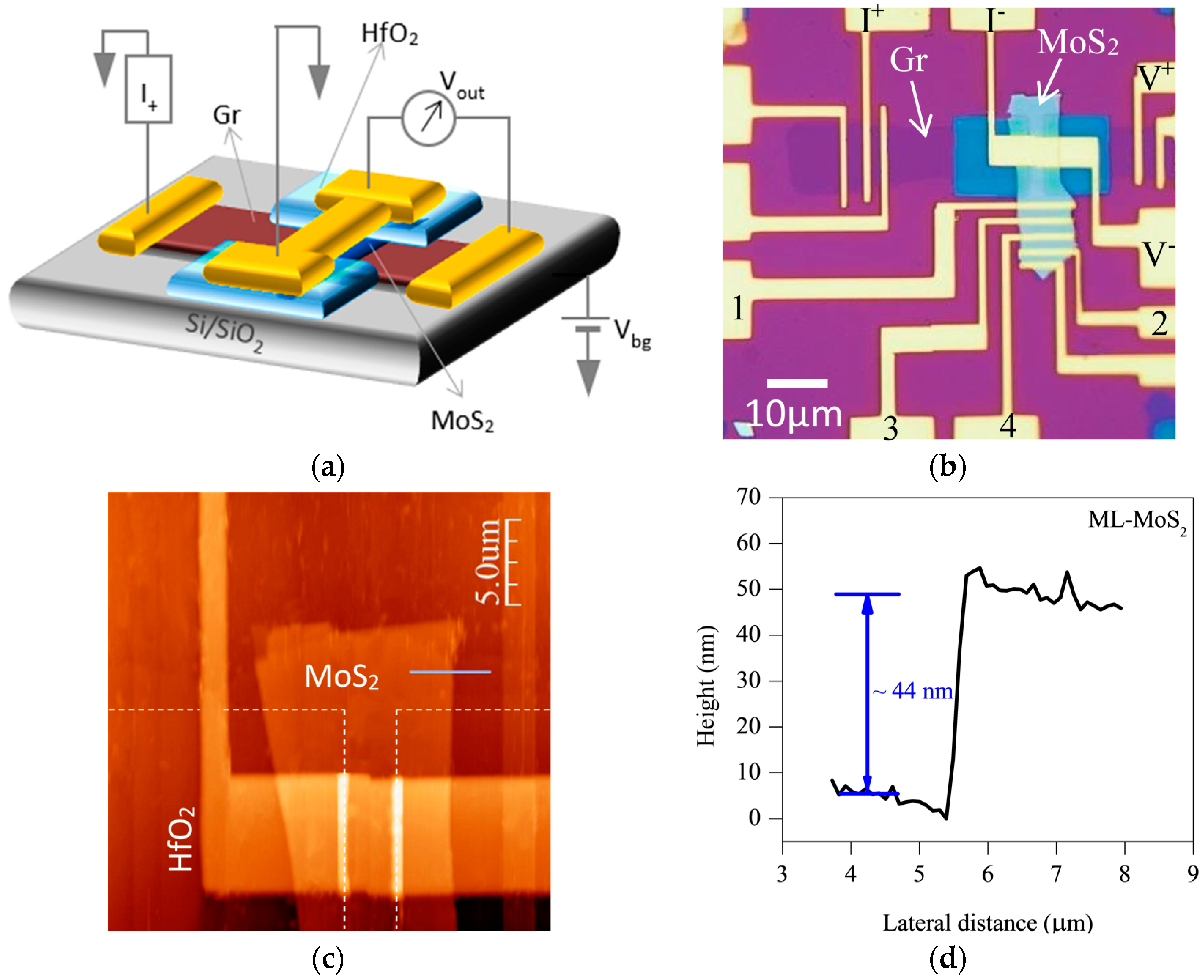
2.1. Device Fabrication

Our Gr/MoS2/(Cr/Au) VFETs were fabricated on SiO2/P+-Si substrate. The thickness of dielectric (SiO2) was 300 nm, whereas P+-Si was used to apply back-gate voltage. In the first process, chemical vapor deposition (CVD) grown graphene was transferred on SiO2/Si substrate using wet transfer method [29], and a graphene Hall bar pattern was defined by using photo-lithography. Then oxygen plasma (power ~50 W) was used for several minutes to etch extraneous graphene. The Raman spectrum for Gr is shown in Supplementary Materials Figure S1 (see Supplementary Materials). In Raman spectrum, 2D to G peak intensity ratio is larger than 3:1, indicating monolayer characteristics of Gr [30]. We used the scotch-tape method for mechanical exfoliation of MoS2 [17,31,32,33,34,35,36,37,38,39,40,41,42,43,44,45]. The suitable MoS2 flake was selected under an optical microscope and then transferred on graphene Hall bar by using micromanipulator. Subsequently, 15-nm-thick HfO2 films was grown by atomic layer deposition on the e-beam lithography defined area. In the last process, e-beam lithography was done to define the top electrode of Cr/Au (8/120 nm).

2.2. Measurements

Electrical measurements were performed by using Keithley 2400 source meter, Keithley 6485K picoammeter, and Keithley 2182A nanovoltmeter. All measurements were performed in vacuum at room temperature. Structural investigation and material identification were performed using Raman spectroscopy and atomic force microscopy (AFM). In Raman spectroscopy, laser wavelength of 514 nm with power below 1 mW was selected to avoid structural degradation caused by the heating effects of the laser. The nominal diameter of laser spot was 0.7 µm.

3. Results and Discussion

3.1. Gr/MoS2/(Cr/Au) Vertical Field-Effect Transistor

A schematic representation of Gr/MoS2/(Cr/Au) VFET is shown in Figure 1a, where the back-gate voltage is applied to control the vertical transport in MoS2 channel. The optical micrograph of device is shown in Figure 1b. Graphene is represented by the purple color, MoS2 by the sky blue, and HfO2 (~15 nm thick) window by the dark blue color. We choose CVD-grown monolayer graphene despite multilayer graphene. We believe that, in case of multilayer graphene, the gate effect would be small as compared to monolayer graphene due to back-gate electric field screening, and modulation in Schottky barrier height will be more difficult as compared to monolayer graphene.
The alphabetic and numeric symbols indicate different contacts used for the planar and vertical transport measurement. Figure 1c shows AFM of MoS2 film, which reveals uniform surface morphology. Height profile taken by AFM shows the thickness of MoS2 to be ~44 nm in Figure 1d.
Raman spectroscopy of MoS2 on monolayer Gr was studied in comparison with MoS2 on Si/SiO2 substrate shown in Supplementary Materials Figure S2. Raman spectrum for MoS2 on Si/SiO2 substrate was represented by the black color, whereas the red color shows Raman spectrum of MoS2 on Gr. Two prominent peaks of MoS2 appeared in the wavenumber range from 380 to 420 cm−1. These two Raman peaks belongs to in-plane ( E 2 g 1 ) and out of plane (A1g) vibrations of “Mo” and “S” atoms [46]. The difference between E 2 g 1 and A1g Raman peaks for MoS2 on Si/SiO2 substrate amounted to Δ ≈ 24 cm−1, indicating a multilayer nature [22]. There was a slight change in peak positions of MoS2 when stacked on Gr. This slight change was due to the relaxation of atoms on different substrate.
We assume that vertical resistance (Rvert) is a cumulative effect of all the resistances including contact resistance and MoS2 channel resistance. We made a cross-junction geometry to investigate the vertical transport in Gr/MoS2/(Cr/Au). The measurements consisted of four-probe technique where two contacts were used as source and drain, while the other two for voltage measurement across VFET. Figure 1b shows the measurement configuration (I+, I, V+, V) for the vertical resistance Rvert. We also measured planar resistance Rplanar of the same MoS2 film using Cr/Au contacts as illustrated by numeric symbols 1, 2, 3, 4 in Figure 1b.

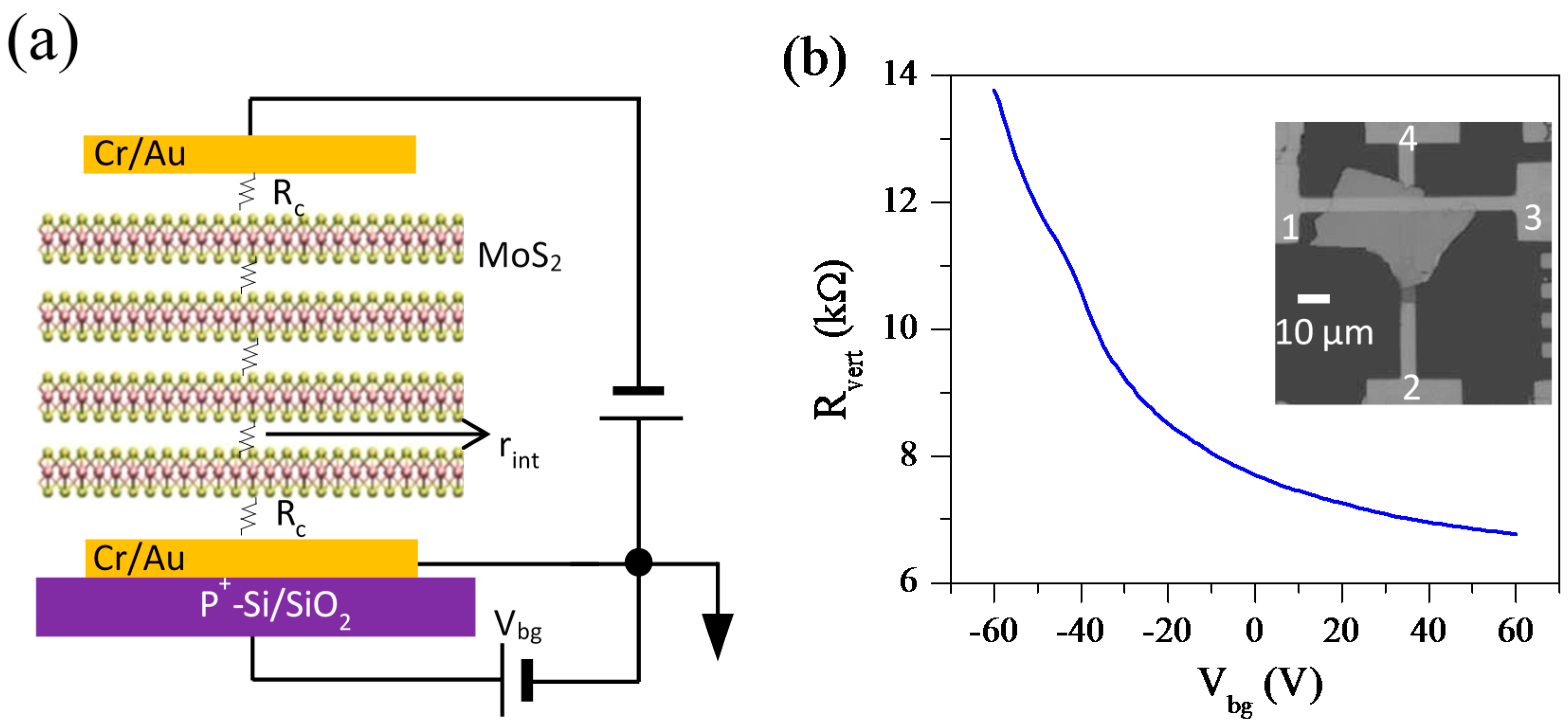
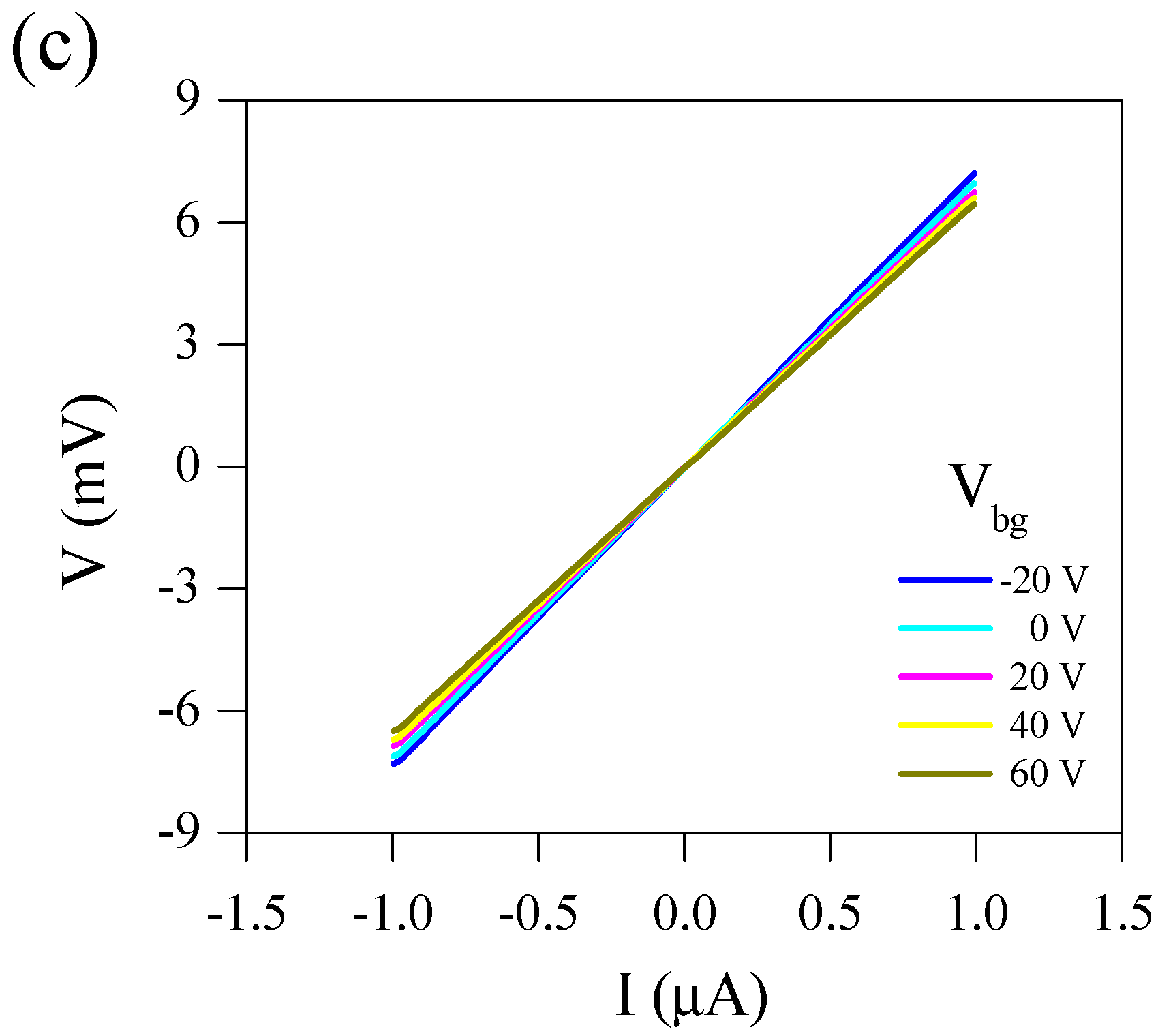
3.2. Vertical Resistance of Gr/MoS2/(Cr/Au) VFET

Figure 2a shows a schematic diagram of Gr/MoS2/(Cr/Au) VFET, where Rint and Rc represent interlayer resistance between stacked layer of MoS2 and contact resistance, respectively. Figure 2b represents vertical resistance (Rvert) of Gr/MoS2/(Cr/Au) VFET as a function of the back-gate voltage (Vbg). In this experiment, the current flows from Gr to the top Cr/Au contact through semiconducting MoS2 channel. The electrical characteristics are strongly modified by Vbg. To understand the physics of the transport mechanism, there are lot of factors that should be keep in mind e.g., Schottky barrier height, barrier width etc. It is a well-known concept that electrical transport in TMD’s based field effect transistors (FET) is governed by either tunneling or thermionic emission. Tunneling is due to passing of carriers through barrier height and is a temperature-independent quantity. However, thermionic emission is highly reliant on temperature. Tunneling current depends upon barrier width, and if the barrier width is too large, we cannot observe tunneling current. Here, our average MoS2 thickness is 50 nm (barrier width ~50 nm). Usually, to observe tunneling mechanism, the barrier width should be ≤5 nm [47]. So, we can firmly say that in our experiment, electrical transport is not caused by tunneling. However, the low value of current observed at Vbg < 0 in our Gr/MoS2 heterostructure’s transport property (shown in Supplementary Materials Figure S3c) is due to gate leakage current and not by the tunneling that is a very well-known phenomenon in Si-based field effect transistors. The Gr/MoS2 junction is completely in off state at low Vbg due to the presence of large Schottky barrier height (SBH), which is why we observed large resistance at that point.
On the other hand, Deshun Qu et al. reported that “S” vacancies in MoS2 play an important role in rint [48]. The importance of “S” atoms was further elaborated for the vertical carrier transport by orbital overlapping between “S” atoms in adjacent layers [49,50].

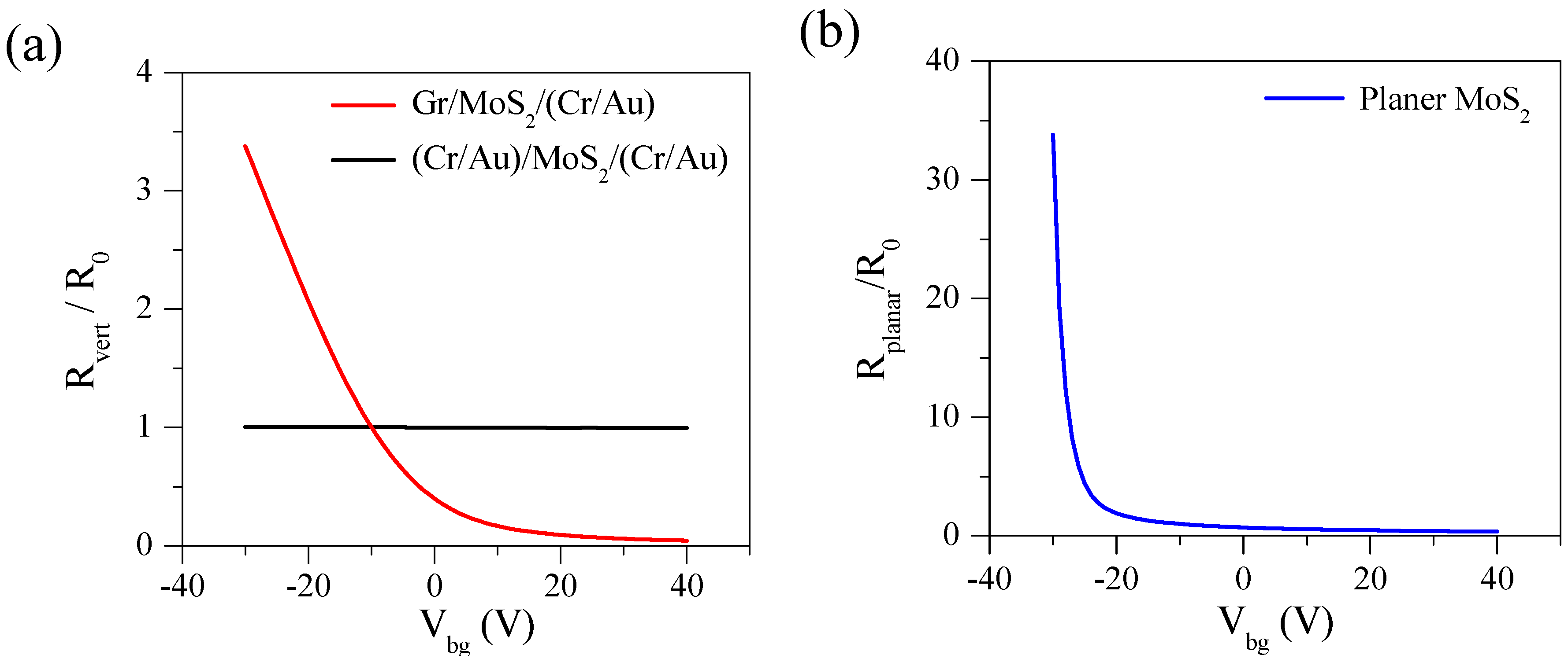
3.3. Resistance Analysis of Gr/MoS2/(Cr/Au) VFET

Rvert in the measurement configuration of Figure 2a can be considered as the sum of interface resistance between Gr and MoS2 ( R Gr / MoS 2 ), total channel resistance of individual layers of MoS2 (RTCR-V), interlayer resistance (Rint) of MoS2, and interface resistance (RSBH) between Cr/Au electrode and MoS2. So, the vertical resistance (Rvert) is given by Equation (1).
Rvert = RTCR-V + Rint + RGR/MoS2 + RSBH
where total interlayer resistance (Rint) is given by R int = Nr int , where N is the total number of layers in MoS2 and rint is the interlayer resistance between two consecutive layers of MoS2. As the thickness of MoS2 increases, Rint increases, and then Rvert increases as well. In the vertical transport, rint is a non-negligible quantity in the thick MoS2 channel. Another important factor that should be elaborated here is the channel resistance itself. In the vertical transport, RTCR-V increases with an increase of the thickness of MoS2 channel. Since both Rint and RTCR-V increase with increasing MoS2 thickness, Rvert shows the dependence of MoS2 thickness. However, the resistance of planar or vertical device depends on cross-sectional area, so it is better to examine resistivity instead of resistance. Figure 2d shows ρ planar and ρ vert as a function of MoS2 thickness.
As another important component of Rvert, we discuss R Gr / MoS 2 which is the interface resistance between Gr and MoS2. We analyze R Gr / MoS 2 within 2D thermionic emission theory, where the Schottky barrier height is given by Equation (2).
Φ B = k B T e ln ( A * T 2 J rev )
where k B is the Boltzmann’s constant, A* is effective Richardson constant and we choose A* = 54 Acm−2 K−2 for MoS2 [51]. We extracted Schottky barrier height at T = 300 K from Ids-Vds curves shown in Supplementary Materials Figure S3. Jrev (=Ids/Ajunc) is the reverse saturation current density at Vds = −0.5 V, where we see a beginning of saturation of Ids. Ajunc (=200 μm2) is the junction area of Gr/MoS2. Barrier height decreases with an increase of Vds or Vbg (see Figure 3a,b). Φ B ranges from 1.10 to 0.78 eV for the interface between monolayer Gr and 53-nm-thick ML-MoS2.
Moreover, planar resistance (Rplanar) of the MoS2 channel was measured by using the electrodes labelled as numeric letters in Figure 1b. While current was applied between 1 and 2, voltage was measured between 3 and 4. Figure 2c shows Rplanar as a function of Vbg. As Vbg increases from −30 to 40 V, Rplanar rapidly decreases, indicating MoS2 is a n-type semiconductor. The MoS2 channel thickness dependence of Rplanar at Vbg = −10 V is shown in Figure 2d. As MoS2 flake thickness increases, Rplanar decreases in contrast to Rvert. We can analyze Rplanar as RTCR-P in 4-probe measurement configuration. Here, RTCR-P represents the in-plane resistance of MoS2. As the thickness of MoS2 channel increases, more layers can contribute to the planar electrical transport, so that total planer channel resistance, RTCR-P decreases. To have an estimate of contact resistivity, we employed transmission line method (TLM) on 51 nm-thick MoS2 flake and extracted contact resistivity to be 0.14 MΩ μm at Vbg = −10 V as shown in Supplementary Materials Figure S4b. The contact resistivity is smaller than the planar resistivity of MoS2 channel itself. So, it is obvious that there are other factors contributing to the total in-plane resistance other than contacts. The back-gate voltage-dependent contact resistivity was also estimated using TLM method as shown in Supplementary Materials Figure S4d. The contact resistivity decreases with Vbg and has a low value in the positive region of Vbg due to the increasing carrier channels.
In lateral devices, the source and drain contacts are directly attached to top surface of MoS2. Therefore, the charge carriers will flow from source to drain mainly through a few top layers of MoS2 due to the interlayer resistance [52,53]. Moreover, since the thickness of MoS2 flake in the lateral device is ~50 nm (about 76 layers), the back-gate electric field will not affect much on the charge carrier transport. This could be the reason of a low Rplaner for thick MoS2 channel in the lateral devices.

3.4. Vertical Transport of (Cr/Au)/Mos2/(Cr/Au) Vertical Field-Effect Transistor

We have studied vertical transport in (Cr/Au)/MoS2/(Cr/Au) VFET, the schematic representation of which is shown in Figure 4a, and inset of Figure 4b shows the scanning electron microscope image. The thickness of MoS2 is about 48 nm. While current bias is applied between 4 and 3, voltage is measured between 2 and 1. Figure 4b shows Rvert as a function of Vbg at room temperature. It shows similar characteristics as Gr/MoS2/(Cr/Au) VFET, but with a low Rvert, which may be due to the low interface resistance between Cr/Au and MoS2. The strong screening of electric field by the bottom Cr/Au electrode creates a weaker dependence on Vbg. The I-V characteristics show almost ohmic behavior at different back-gate voltages (see Figure 4c).
Although Rvert of (Cr/Au)/MoS2/(Cr/Au) VFET in Figure 4b decreases as Vbg is increased, the relative change of Rvert is rather small. To compare the relative change of Rvert we obtain Rvert/R0 as a function of Vbg, where R0 at Vbg = −10 V is taken as a reference resistance. Figure 5a shows Rvert/R0 as a function of Vbg for Gr/MoS2/(Cr/Au) and (Cr/Au)/MoS2/(Cr/Au) VFETs. The thickness of MoS2 is 50 nm and 48 nm for Gr/MoS2/(Cr/Au) and (Cr/Au)/MoS2/(Cr/Au) VFETs, respectively. Of note, Vbg does not significantly affect transport characteristics in (Cr/Au)/MoS2/(Cr/Au) VFET, because the bottom Cr/Au electrode effectively screens the electric field from the Vbg application. However, Rvert/R0 has a strong dependence on Vbg in Gr/MoS2/(Cr/Au) devices, due to the weak screening of the electric field by bottom monolayer Gr. For comparison, we also present Rplanar/R0 as a function of Vbg in Figure 5b. A rapid increase of Rplanar/R0 below Vbg = −30 V indicates the threshold voltage of n-type MoS2 channel in our devices. The dependence of Rplanar/R0 on Vbg is much larger than VFETs, asMoS2 channel is directly affected by Vbg application in ordinary planar geometry.
In the positive region of Vbg, both resistances in planar (in-plane) and vertical configuration show a similar dependence of Vbg. However, at negative Vbg, we find different dependences of Vbg as seen in Figure 5a,b. In Figure 5a Rvert/R0 shows an exponential dependence of Vbg for Gr/MoS2/(Cr/Au) VFET with 50 nm-thick MoS2 flake. This might be due to the gate-voltage dependent density of states in graphene, which affects the interface resistance between graphene and MoS2. In case of (Cr/Au)/MoS2/(Cr/Au) VFET with 50 nm-thick MoS2, there exists large screening effect by the bottom Cr/Au electrode that does not allow the back-gate electric field to influence on the electronic transport. On the other hand, in case of planar 48 nm-thick MoS2 FET of Figure 5b, we have source/drain (Cr/Au) electrodes directly on the lateral channel of MoS2. At a particular negative Vbg, the channel transport is in off-state, so resistance increases rapidly at Vbg below the threshold voltage.

4. Conclusions

In the present study, we performed four probe measurements using cross-junction geometry of Gr/MoS2/(Cr/Au) VFETs. We were able to achieve gate-tunable transport characteristics in VFETs. Since the bottom Gr allows the electric field to reach MoS2 channel, the vertical resistance (Rvert) of Gr/MoS2/(Cr/Au) VFET can be effectively modified by Vbg. The vertical transport characteristics are examined as compared to those of the ordinary lateral MoS2 field-effect transistor. Rvert increases as the thickness of MoS2 increases, whereas Rplanar decreases. The increase of Rvert in the thicker MoS2 film can be attributed to the interlayer resistance in the vertical direction. However, Rplanar shows a lower value for a thicker MoS2 film because of excess of charge carriers available in upper layers connected directly to source/drain contacts and cumulative contribution of low Rint from the lower layers. In planer geometry only, layers attached near to channel layer (on which source/drain electrodes are constructed) are the main source of the conduction mechanism. Schottky barrier height at Gr/MoS2 interface can be analyzed from the Ids-Vds curve. The Schottky barrier height decreases as Vbg or Vds increases. Vbg does not affect transport characteristics much in (Cr/Au)/MoS2/(Cr/Au) VFET, because the bottom Cr/Au electrode effectively screens the electric field from the Vbg application. However, a strong dependence on Vbg in Gr/MoS2/(Cr/Au) devices was observed due to the weak screening of electric field by bottom Gr. We believe that gate tunable VFET will serve as one of important components for future 2D materials electronics.

Supplementary Materials

The following are available online at www.mdpi.com/2079-4991/8/1/14/s1.

Acknowledgments

This research was supported by Priority Research Center Program (2010-0020207) and Basic Science Research Program (2016R1D1A1A09917762) through the National Research Foundation of Korea funded by the Ministry of Education.

Author Contributions

J.E. and G.N. conceived and designed the experiment; M.F.K., S.A., G.D. and A.M.A. contributed to device fabrication and measurement. M.A.R. carried out ALD process to grow HfO2. Y.S. and J.E. contributed to discussion of the manuscript. G.N. and J.E. wrote the manuscript.

Conflicts of Interest

The authors declare no conflict of interest.

References

  1. Dean, C.; Young, A.; Wang, L.; Meric, I.; Lee, G.-H.; Watanabe, K.; Taniguchi, T.; Shepard, K.; Kim, P.; Hone, J. Graphene based heterostructures. Solid State Commun. 2012, 152, 1275–1282. [Google Scholar] [CrossRef]
  2. Tan, J.; Avsar, A.; Balakrishnan, J.; Koon, G.; Taychatanapat, T.; O’Farrell, E.; Watanabe, K.; Taniguchi, T.; Eda, G.; Castro Neto, A. Electronic transport in graphene-based heterostructures. Appl. Phys. Lett. 2014, 104, 183504. [Google Scholar] [CrossRef]
  3. Georgiou, T.; Jalil, R.; Belle, B.D.; Britnell, L.; Gorbachev, R.V.; Morozov, S.V.; Kim, Y.-J.; Gholinia, A.; Haigh, S.J.; Makarovsky, O. Vertical field-effect transistor based on graphene-WS2 heterostructures for flexible and transparent electronics. Nat. Nanotechnol. 2013, 8, 100–103. [Google Scholar] [CrossRef] [PubMed]
  4. Fiori, G.; Betti, A.; Bruzzone, S.; Iannaccone, G. Lateral graphene-hBCN heterostructures as a platform for fully two-dimensional transistors. ACS Nano 2012, 6, 2642–2648. [Google Scholar] [CrossRef] [PubMed]
  5. Liu, Z.; Ma, L.; Shi, G.; Zhou, W.; Gong, Y.; Lei, S.; Yang, X.; Zhang, J.; Yu, J.; Hackenberg, K.P. In-plane heterostructures of graphene and hexagonal boron nitride with controlled domain sizes. Nat. Nanotechnol. 2013, 8, 119–124. [Google Scholar] [CrossRef] [PubMed]
  6. Moon, J.S.; Seo, H.; Stratan, F.; Antcliffe, M.; Schmitz, A.; Ross, R.S.; Kiselev, A.A.; Wheeler, V.D.; Nyakiti, L.O.; Gaskill, D.K. Lateral graphene heterostructure field-effect transistor. IEEE Electron Device Lett. 2013, 34, 1190–1192. [Google Scholar] [CrossRef]
  7. Zhang, W.; Chuu, C.-P.; Huang, J.-K.; Chen, C.-H.; Tsai, M.-L.; Chang, Y.-H.; Liang, C.-T.; Chen, Y.-Z.; Chueh, Y.-L.; He, H., Jr.; et al. Ultrahigh-gain photodetectors based on atomically thin graphene-MoS2 heterostructures. Sci. Rep. 2014, 4, 3826. [Google Scholar] [CrossRef] [PubMed]
  8. Yu, W.J.; Liu, Y.; Zhou, H.; Yin, A.; Li, Z.; Huang, Y.; Duan, X. Highly efficient gate-tunable photocurrent generation in vertical heterostructures of layered materials. Nat. Nanotechnol. 2013, 8, 952–958. [Google Scholar] [CrossRef] [PubMed]
  9. Geim, A.K.; Grigorieva, I.V. Van der waals heterostructures. arXiv, 2013; arXiv:1307.6718. [Google Scholar]
  10. Gong, Y.; Lin, J.; Wang, X.; Shi, G.; Lei, S.; Lin, Z.; Zou, X.; Ye, G.; Vajtai, R.; Yakobson, B.I. Vertical and in-plane heterostructures from WS2/MoS2 monolayers. Nat. Mater. 2014, 13, 1135–1142. [Google Scholar] [CrossRef] [PubMed]
  11. Lee, C.-H.; Lee, G.-H.; Van Der Zande, A.M.; Chen, W.; Li, Y.; Han, M.; Cui, X.; Arefe, G.; Nuckolls, C.; Heinz, T.F. Atomically thin p–n junctions with van der waals heterointerfaces. Nat. Nanotechnol. 2014, 9, 676–681. [Google Scholar] [CrossRef] [PubMed]
  12. Torres, T. Graphene chemistry. Chem. Soc. Rev. 2017, 46, 4385–4386. [Google Scholar] [CrossRef] [PubMed]
  13. Britnell, L.; Gorbachev, R.; Jalil, R.; Belle, B.; Schedin, F.; Mishchenko, A.; Georgiou, T.; Katsnelson, M.; Eaves, L.; Morozov, S. Field-effect tunneling transistor based on vertical graphene heterostructures. Science 2012, 335, 947–950. [Google Scholar] [CrossRef] [PubMed] [Green Version]
  14. Myoung, N.; Seo, K.; Lee, S.J.; Ihm, G. Large current modulation and spin-dependent tunneling of vertical graphene/MoS2 heterostructures. ACS Nano 2013, 7, 7021–7027. [Google Scholar] [CrossRef] [PubMed]
  15. Roy, K.; Padmanabhan, M.; Goswami, S.; Sai, T.P.; Ramalingam, G.; Raghavan, S.; Ghosh, A. Graphene-MoS2 hybrid structures for multifunctional photoresponsive memory devices. Nat. Nanotechnol. 2013, 8, 826–830. [Google Scholar] [CrossRef] [PubMed]
  16. Yu, L.; Lee, Y.-H.; Ling, X.; Santos, E.J.; Shin, Y.C.; Lin, Y.; Dubey, M.; Kaxiras, E.; Kong, J.; Wang, H. Graphene/MoS2 hybrid technology for large-scale two-dimensional electronics. Nano Lett. 2014, 14, 3055–3063. [Google Scholar] [CrossRef] [PubMed]
  17. Bertolazzi, S.; Krasnozhon, D.; Kis, A. Nonvolatile memory cells based on MoS2/graphene heterostructures. ACS Nano 2013, 7, 3246–3252. [Google Scholar] [CrossRef] [PubMed]
  18. Cho, B.; Yoon, J.; Lim, S.K.; Kim, A.R.; Kim, D.-H.; Park, S.-G.; Kwon, J.-D.; Lee, Y.-J.; Lee, K.-H.; Lee, B.H. Chemical sensing of 2D graphene/MoS2 heterostructure device. ACS Appl. Mater. Interfaces 2015, 7, 16775–16780. [Google Scholar] [CrossRef] [PubMed]
  19. Moriya, R.; Yamaguchi, T.; Inoue, Y.; Morikawa, S.; Sata, Y.; Masubuchi, S.; Machida, T. Large current modulation in exfoliated-graphene/MoS2/metal vertical heterostructures. Appl. Phys. Lett. 2014, 105, 083119. [Google Scholar] [CrossRef]
  20. Tian, H.; Tan, Z.; Wu, C.; Wang, X.; Mohammad, M.A.; Xie, D.; Yang, Y.; Wang, J.; Li, L.-J.; Xu, J. Novel field-effect schottky barrier transistors based on graphene-MoS2 heterojunctions. Sci. Rep. 2014, 4, 5951. [Google Scholar] [CrossRef] [PubMed]
  21. Shih, C.-J.; Wang, Q.H.; Son, Y.; Jin, Z.; Blankschtein, D.; Strano, M.S. Tuning on-off current ratio and field-effect mobility in a MoS2-graphene heterostructure via schottky barrier modulation. ACS Nano 2014, 8, 5790–5798. [Google Scholar] [CrossRef] [PubMed]
  22. Khan, M.F.; Shehzad, M.A.; Iqbal, M.Z.; Iqbal, M.W.; Nazir, G.; Seo, Y.; Eom, J. A facile route to a high-quality graphene/MoS2 vertical field-effect transistor with gate-modulated photocurrent response. J. Mater. Chem. C 2017, 5, 2337–2343. [Google Scholar] [CrossRef]
  23. Yu, W.J.; Li, Z.; Zhou, H.; Chen, Y.; Wang, Y.; Huang, Y.; Duan, X. Vertically stacked multi-heterostructures of layered materials for logic transistors and complementary inverters. Nat. Mater. 2013, 12, 246. [Google Scholar] [CrossRef] [PubMed]
  24. Sata, Y.; Moriya, R.; Yamaguchi, T.; Inoue, Y.; Morikawa, S.; Yabuki, N.; Masubuchi, S.; Machida, T. Modulation of schottky barrier height in graphene/MoS2/metal vertical heterostructure with large current on–off ratio. Jpn. J. Appl. Phys. 2015, 54, 04DJ04. [Google Scholar] [CrossRef]
  25. Yoon, J.; Park, W.; Bae, G.Y.; Kim, Y.; Jang, H.S.; Hyun, Y.; Lim, S.K.; Kahng, Y.H.; Hong, W.K.; Lee, B.H. Highly flexible and transparent multilayer MoS2 transistors with graphene electrodes. Small 2013, 9, 3295–3300. [Google Scholar] [CrossRef] [PubMed]
  26. Du, H.; Kim, T.; Shin, S.; Kim, D.; Kim, H.; Sung, J.H.; Lee, M.J.; Seo, D.H.; Lee, S.W.; Jo, M.-H. Schottky barrier contrasts in single and bi-layer graphene contacts for MoS2 field-effect transistors. Appl. Phys. Lett. 2015, 107, 233106. [Google Scholar] [CrossRef]
  27. Dathbun, A.; Kim, Y.; Kim, S.; Yoo, Y.; Kang, M.S.; Lee, C.; Cho, J.H. Large-Area CVD-Grown Sub-2 V ReS2 Transistors and Logic Gates. Nano Lett. 2017, 17, 2999–3005. [Google Scholar] [CrossRef] [PubMed]
  28. Liu, Y.; Wu, H.; Cheng, H.-C.; Yang, S.; Zhu, E.; He, Q.; Ding, M.; Li, D.; Guo, J.; Weiss, N.O. Toward barrier free contact to molybdenum disulfide using graphene electrodes. Nano Lett. 2015, 15, 3030–3034. [Google Scholar] [CrossRef] [PubMed]
  29. Li, X.; Zhu, Y.; Cai, W.; Borysiak, M.; Han, B.; Chen, D.; Piner, R.D.; Colombo, L.; Ruoff, R.S. Transfer of large-area graphene films for high-performance transparent conductive electrodes. Nano Lett. 2009, 9, 4359–4363. [Google Scholar] [CrossRef] [PubMed]
  30. Zhang, L.; Yan, Y.; Wu, H.-C.; Yu, D.; Liao, Z.-M. Gate-tunable tunneling resistance in graphene/topological insulator vertical junctions. ACS Nano 2016, 10, 3816–3822. [Google Scholar] [CrossRef] [PubMed]
  31. Chhowalla, M.; Shin, H.S.; Eda, G.; Li, L.-J.; Loh, K.P.; Zhang, H. The chemistry of two-dimensional layered transition metal dichalcogenide nanosheets. Nat. Chem. 2013, 5, 263–275. [Google Scholar] [CrossRef] [PubMed]
  32. Mak, K.F.; Lee, C.; Hone, J.; Shan, J.; Heinz, T.F. Atomically thin MoS2: A new direct-gap semiconductor. Phys. Rev. Lett. 2010, 105, 136805. [Google Scholar] [CrossRef] [PubMed]
  33. Zhao, Y.; Luo, X.; Li, H.; Zhang, J.; Araujo, P.T.; Gan, C.K.; Wu, J.; Zhang, H.; Quek, S.Y.; Dresselhaus, M.S. Interlayer breathing and shear modes in few-trilayer MoS2 and WSe2. Nano Lett. 2013, 13, 1007–1015. [Google Scholar] [CrossRef] [PubMed]
  34. Splendiani, A.; Sun, L.; Zhang, Y.; Li, T.; Kim, J.; Chim, C.-Y.; Galli, G.; Wang, F. Emerging photoluminescence in monolayer MoS2. Nano Lett. 2010, 10, 1271–1275. [Google Scholar] [CrossRef] [PubMed]
  35. Li, H.; Qi, X.; Wu, J.; Zeng, Z.; Wei, J.; Zhang, H. Investigation of MoS2 and graphene nanosheets by magnetic force microscopy. ACS Nano 2013, 7, 2842–2849. [Google Scholar] [CrossRef] [PubMed]
  36. Yin, Z.; Li, H.; Li, H.; Jiang, L.; Shi, Y.; Sun, Y.; Lu, G.; Zhang, Q.; Chen, X.; Zhang, H. Single-layer MoS2 phototransistors. ACS Nano 2011, 6, 74–80. [Google Scholar] [CrossRef] [PubMed]
  37. Lopez-Sanchez, O.; Lembke, D.; Kayci, M.; Radenovic, A.; Kis, A. Ultrasensitive photodetectors based on monolayer MoS2. Nat. Nanotechnol. 2013, 8, 497–501. [Google Scholar] [CrossRef] [PubMed]
  38. Zeng, H.; Dai, J.; Yao, W.; Xiao, D.; Cui, X. Valley polarization in MoS2 monolayers by optical pumping. Nat. Nanotechnol. 2012, 7, 490–493. [Google Scholar] [CrossRef] [PubMed]
  39. Mak, K.F.; He, K.; Shan, J.; Heinz, T.F. Control of valley polarization in monolayer MoS2 by optical helicity. Nat. Nanotechnol. 2012, 7, 494–498. [Google Scholar] [CrossRef] [PubMed]
  40. Radisavljevic, B.; Radenovic, A.; Brivio, J.; Giacometti, V.; Kis, A. Single-layer MoS2 transistors. Nat. Nanotechnol. 2011, 6, 147–150. [Google Scholar] [CrossRef] [PubMed]
  41. Li, H.; Yin, Z.; He, Q.; Li, H.; Huang, X.; Lu, G.; Fam, D.W.H.; Tok, A.I.Y.; Zhang, Q.; Zhang, H. Fabrication of single-and multilayer MoS2 film-based field-effect transistors for sensing no at room temperature. Small 2012, 8, 63–67. [Google Scholar] [CrossRef] [PubMed]
  42. Lee, H.S.; Min, S.-W.; Chang, Y.-G.; Park, M.K.; Nam, T.; Kim, H.; Kim, J.H.; Ryu, S.; Im, S. MoS2 nanosheet phototransistors with thickness-modulated optical energy gap. Nano Lett. 2012, 12, 3695–3700. [Google Scholar] [CrossRef] [PubMed]
  43. Kim, S.; Konar, A.; Hwang, W.-S.; Lee, J.H.; Lee, J.; Yang, J.; Jung, C.; Kim, H.; Yoo, J.-B.; Choi, J.-Y. High-mobility and low-power thin-film transistors based on multilayer MoS2 crystals. Nat. Commun. 2012, 3, 1011. [Google Scholar] [CrossRef] [PubMed]
  44. Li, H.; Lu, G.; Yin, Z.; He, Q.; Li, H.; Zhang, Q.; Zhang, H. Optical identification of single-and few-layer MoS2 sheets. Small 2012, 8, 682–686. [Google Scholar] [CrossRef] [PubMed]
  45. Castellanos-Gomez, A.; Barkelid, M.; Goossens, A.; Calado, V.E.; van der Zant, H.S.; Steele, G.A. Laser-thinning of MoS2: On demand generation of a single-layer semiconductor. Nano Lett. 2012, 12, 3187–3192. [Google Scholar] [CrossRef] [PubMed]
  46. Lee, C.; Yan, H.; Brus, L.E.; Heinz, T.F.; Hone, J.; Ryu, S. Anomalous lattice vibrations of single-and few-layer MoS2. ACS Nano 2010, 4, 2695–2700. [Google Scholar] [CrossRef] [PubMed]
  47. Li, H.-M.; Lee, D.; Qu, D.; Liu, X.; Ryu, J.; Seabaugh, A.; Yoo, W.J. Ultimate thin vertical p–n junction composed of two-dimensional layered molybdenum disulfide. Nat. Commun. 2015, 6, 6564. [Google Scholar] [CrossRef] [PubMed]
  48. Qu, D.; Liu, X.; Ahmed, F.; Lee, D.; Yoo, W.J. Self-screened high performance multi-layer MoS2 transistor formed by using a bottom graphene electrode. Nanoscale 2015, 7, 19273–19281. [Google Scholar] [CrossRef] [PubMed]
  49. Nguyen, L.-N.; Lan, Y.-W.; Chen, J.-H.; Chang, T.-R.; Zhong, Y.-L.; Jeng, H.-T.; Li, L.-J.; Chen, C.-D. Resonant tunneling through discrete quantum states in stacked atomic-layered MoS2. Nano Lett. 2014, 14, 2381–2386. [Google Scholar] [CrossRef] [PubMed]
  50. Nayak, A.P.; Bhattacharyya, S.; Zhu, J.; Liu, J.; Wu, X.; Pandey, T.; Jin, C.; Singh, A.K.; Akinwande, D.; Lin, J.-F. Pressure-induced semiconducting to metallic transition in multilayered molybdenum disulphide. Nat. Commun. 2014, 5, 3731. [Google Scholar] [CrossRef] [PubMed]
  51. Lin, Y.-F.; Li, W.; Li, S.-L.; Xu, Y.; Aparecido-Ferreira, A.; Komatsu, K.; Sun, H.; Nakaharai, S.; Tsukagoshi, K. Barrier inhomogeneities at vertically stacked graphene-based heterostructures. Nanoscale 2014, 6, 795–799. [Google Scholar] [CrossRef] [PubMed]
  52. Kim, S.W.; Na, J.H.; Choi, W.L.; Chung, H.-J.; Jhang, S.H. Nonuniform current distribution between individual layers of multilayer MoS2, experimentally approached by using a laser thinning technique. J. Korean Phys. Soc. 2016, 69, 1497–1501. [Google Scholar] [CrossRef]
  53. Das, S.; Appenzeller, J. Where does the current flow in two-dimensional layered systems? Nano Lett. 2013, 13, 3396–3402. [Google Scholar] [CrossRef] [PubMed]
Figure 1. (a) Schematic representation of Gr/MoS2/(Cr/Au) vertical field-effect transistor (VFET) (b) Optical image of Gr/MoS2/(Cr/Au) VFET. Two HfO2 windows on top of Gr/MoS2 layer define the junction region. Different contacts with alphabetic and numeric letters were used to measure Rvert and Rplaner, respectively (c) Atomic force microscope image that clearly reveals multilayer MoS2 (ML-MoS2) flake with top Cr/Au contact. HfO2 windows are highlighted by dashed lines. (d) Height profile of ML-MoS2 shows the thickness of nearly 44 nm.
Nanomaterials 08 00014 g001
Figure 2. (a) Schematic diagram for resistances to compose Gr/MoS2/(Cr/Au) vertical field-effect transistor (VFET) with 50 nm-thick MoS2. (b) Vertical Resistance (Rvert) as a function of the back-gate voltage (Vbg) for Gr/MoS2/(Cr/Au) VFET with 50 nm-thick MoS2. (c) Planar resistance (Rplanar) as a function of Vbg for the lateral MoS2 field-effect transistor with 48 nm-thick MoS2. (d) Dependence of ρ planar and ρ vert on the thickness of MoS2 channels at Vbg = −10 V.
Nanomaterials 08 00014 g002
Figure 3. (a) Schottky barrier height (ϕB) at T = 300 K between monolayer Gr and 53-nm-thick ML-MoS2 as a function of Vds at different Vbg’s from −20 to 40 V with equal step of 10 V. (b) ϕB at T = 300 K as a function of Vbg at Vds = 1, 1.5, and 2 V.
Nanomaterials 08 00014 g003
Figure 4. (a) Schematic diagram of the resistances to compose (Cr/Au)/MoS2/(Cr/Au) vertical field-effect transistor (VFET). The thickness of MoS2 is 48 nm. (b) Rvert as a function of Vbg for (Cr/Au)/MoS2/(Cr/Au) VEFT. Inset: A scanning electron microscope image of the device. While the constant current of 1 μA is applied between 1 and 4, voltage is measured between 2 and 3. (c) I-V characteristics at different Vbg’s.
Nanomaterials 08 00014 g004aNanomaterials 08 00014 g004b
Figure 5. (a) Rvert/R0 as a function of Vbg. While the thickness of MoS2 is 50 nm for Gr/MoS2/(Cr/Au) VEFT, the thickness of MoS2 is 48 nm for (Cr/Au)/MoS2/(Cr/Au) VEFT. (b) Rplanar/R0 as a function of Vbg for 48 nm-thick MoS2 in planar geometry. Reference resistances (R0) were taken at Vbg = −10 V. All measurements were done at T = 300 K.
Nanomaterials 08 00014 g005

