Nanoporous Structure Formation on the Surface of InSb by Ion Beam Irradiation

1
School of Environmental Science and Technology, Kochi University of Technology, Tosayamada, Kami, Kochi 782-8502, Japan
2
Center for Nanotechnology, Research Institute, Kochi University of Technology, Tosayamada, Kami, Kochi 782-8502, Japan
*
Author to whom correspondence should be addressed.
Nanomaterials 2017, 7(8), 204; https://doi.org/10.3390/nano7080204
Submission received: 6 May 2017
/
Revised: 23 July 2017
/
Accepted: 26 July 2017
/
Published: 30 July 2017
Abstract
:Nanoporous structures have a great potential for application in electronic and photonic materials, including field effect transistors, photonic crystals, and quantum dots. The control of size and shape is important for such applications. In this study, nanoporous structure formation on the indium antimonide (InSb) surface was investigated using controlled focused ion beam irradiation. Upon increasing the ion dose, the structures grew larger, and the shapes changed from voids to pillars. The structures also became larger when the ion flux (high-dose) and accelerating voltage were increased. The structure grew obliquely on the substrate by following the ion beam irradiation of 45°. The shapes of the structures formed by superimposed ion beam irradiation were affected by primary irradiation conditions. The nanostructural features on the InSb surface were easy to control by changing the ion beam conditions.
1. Introduction
Nanoporous structures on semiconductor surfaces have a great potential for application in electronic and photonic materials, including field effect transistors (FETs), photonic crystals, and quantum dots. In these materials, both the FET gate length and the quantum dot size must be less than 20 nm and the photonic crystals must be approximately 200 nm in size. Controlling the nanoporous structure size and shape is important for such applications. In this study, nanoporous structure formation is investigated on the surface of indium antimonide (InSb) by using controlled focused ion beam (FIB) irradiation. InSb is a narrow-gap (direct-gap) compound semiconductor with a band gap of 0.17 eV and can be applied in electro-photonic devices. Nanoporous structure formation on InSb using ion beam irradiation has been reported [1,2,3,4,5,6,7,8,9], and the structures obtained were similar to those formed on materials such as gallium antimonide (GaSb) [1,10,11,12,13,14,15,16,17,18], germanium (Ge) [19,20,21,22,23,24,25,26,27], Si1−xGex alloys [28], and GaAs1−xSbx alloys [29]. The formation mechanisms on these materials are dominated by the self-assembly of irradiation-induced point defects (Frenkel pairs, an interstitial atom, and a vacancy). Many point defects are generated near the surface by the collision cascade under ion irradiation. Small voids or elevations are formed in the early stage of irradiation. The surface roughness increases through the migration of vacancies and interstitials, thus resulting in the formation of nanoporous structures on the surface. Herein, we report the effects of ion beam conditions (ion beam dose, flux, accelerating voltage, and irradiation angle) on the sizes and shapes of the resulting nanoporous structures. In addition, the effects of superimposed ion beam irradiation were examined using different ion beam doses in the first and second irradiations. The accelerator was used for FIB, which was easy to change ion beam conditions.
2. Experimental Procedure
A mirror-polished InSb single-crystal wafer with (001) orientation was used for irradiation. Ion irradiation was performed using an FIB (FEI QUANTA 3D 200i). The ion species was Ga+. The accelerating voltages were 16 and 30 kV. The ion beam doses were 1 × 10¹⁷–1 × 10²⁰ ions/m2, and the ion beam fluxes were 1.5 × 10¹⁸–2.7 × 10¹⁹ ions/m2 s. The wafers were kept at room temperature during the experiments. The irradiation angles were 0° and 45°. The chamber vacuum was ~4 × 10⁻⁴ Pa. Irradiation with Ga+ ions was carried out in image scanning mode; Ga was irradiated at 512 × 441 dots in an area of 12.5 × 10.8 μm in one scan. Structural changes during ion beam irradiation were observed by field-emission scanning electron microscopy (FE-SEM; JEOL JSM-7401F). Elemental analysis was performed by energy-dispersive X-ray spectroscopy (EDX; HITACHI SU8020 powered by HORIBA EMAX ENERGY EX-250 (X-Max80). The projection ranges of the Ga+ ions and the average number of vacancies produced per incident ion on the InSb surface were estimated to be 14 nm and 1281 vacancies/ion, 17 nm and 2383 vacancies/ion, and 17 nm and 2270 vacancies/ion at 16 kV, 30 kV, and 30 kV with 45 degrees tilt, respectively. These values were estimated by stopping and range of ions in matter (SRIM) simulation [30,31] using the displacement threshold energy values of Bauerlein (5.8 eV for In and 6.8 eV for Sb) [32].
3. Results and Discussion
Figure 1 shows the surface SEM images of InSb irradiated with 30 kV Ga+ ions at low flux. No structures were observed on the surfaces at the dose of 1 × 10¹⁷ ions/m2 scan (Figure 1a–e). At the dose of 1 × 10¹⁸ ions/m2 scan (Figure 1f–j), voids were observed on some parts of the surface (Figure 1h–j). With increasing ion dose, voids grew and increased in density. The average void diameter was 31 nm in Figure 1i and 34 nm in Figure 1j. At a dose of 1 × 10¹⁹ ions/m2 scan (Figure 1k–o), voids were observed in all scans. In Figure 1k, small voids (average diameter: 26 nm) were formed all over the InSb surface. The void diameter became large with increasing ion dose. The average void diameter was 72 nm in Figure 1m and 115 nm in Figure 1o. The void shape changed from round to not round. The surface had voids in addition to roughness. Under high-dose irradiation (1 × 10¹⁹ ions/m2 scan; Figure 1p–t), pillar structures were observed instead of voids. Whereas the voids formed via vacancy aggregation [12], the pillars formed from re-deposition resulting from ion beam sputtering [5,6]. In this experiment, those phenomena depended on different ion doses. Different ion dose irradiation induced changes in the features of the structure features. The pillar had a facet in the structure. It was shown that the pillar was made via recrystallization by sputtered atoms.
Figure 2 shows surface SEM images of InSb irradiated with 30 kV Ga+ ions at high-flux irradiation. Compared to the images in Figure 1 (low-flux irradiation), voids were formed on the surface irradiated at doses of 1 × 10¹⁷ ions/m2 scan, as shown in Figure 2d,e (low dose). In Figure 2g–j, irradiated at a dose of 1 × 10¹⁸ ions/m2 scan, the voids also were formed. The average void diameter was 45 nm in Figure 2i and 33 nm in Figure 2j. Voids were formed at a dose of 1 × 10¹⁹ ions/m2 scan (Figure 2k–o); the average void diameter was 24 nm in Figure 2k, 69 nm in Figure 2m, and 122 nm in Figure 2o. As the ion dose increased, the small voids observed in Figure 2k disappeared, and the size of the resultant structure became larger; thus, the trends observed with increasing dose were the same as those seen in low-flux irradiation. However, the void and pillar sizes were larger under high-flux irradiation than under low-flux irradiation. High flux was effective at producing large structures. This is because it was thought that the induced vacancies presented with dense distribution under the surface in the short time. The vacancies could easily aggregate, resulting in large voids under high-flux irradiation. In addition, highly efficient sputtering and re-deposition also occurred under high-flux irradiation.
The diameters of the void structures on the InSb samples observed in Figure 1 and Figure 2 are presented as a function of irradiation dose in Figure 3. The void diameter appears to increase roughly linearly with the ion dose. For low doses, the points are all clumped together. The void dimensions under high-flux irradiation were larger than under low-flux in high-dose irradiation.
Figure 4 shows surface SEM images of InSb irradiated with a 30 kV Ga+ ion beam at the same dose (1 × 10²⁰ ions/m2 scan) under different fluxes. The effect of flux was examined for high-dose irradiation. A comparison of the samples irradiated at low flux (1.5 × 10¹⁸ ions/m2 s; Figure 4a–e (reshown as Figure 1p–t)) and high flux (5.3 × 10¹⁸ ions/m2 s; Figure 4f–j (reshown as Figure 2p–t)) indicates that the pillar structures became larger with increasing ion flux. However, the pillar structures were small in most samples irradiated at high flux (Figure 4k–o). The formation of the pillar structures was dominated by re-deposition resulting from ion beam sputtering. At low and high flux, irradiation enhanced re-deposition, and at the highest flux, irradiation enhanced the structure of sputtering.
Figure 5 shows the surface SEM images of InSb irradiated with Ga+ ions at a dose of 1 × 10²⁰ ions/m2 scan and accelerating voltages of 16 kV (Figure 5a–e) and 30 kV (Figure 5f–j (reshown as Figure 4k–o)). The pillar size for the accelerating voltage of 30 kV was larger than that obtained at 16 kV, whereas the pillar density was lower. The total sputtering yields (atoms per ion) of In and Sb on InSb irradiated with Ga+ ions were calculated by SRIM simulation [30,31,32], and are summarized in Table 1. The total number of atoms per ion is smaller for the accelerating voltage of 16 kV (7.975 atoms/ion) than for 30 kV (8.537 atoms/ion). Thus, larger structures are expected to form on samples irradiated at 30 kV.
Figure 6 shows the surface SEM images of InSb irradiated with a 30 kV Ga+ ion beam at a dose of 1 × 10²⁰ ions/m2 scan and different irradiation angles: 0° (Figure 6a–e (reshown as Figure 2f–j) and Figure 6k–o (reshown as Figure 2p–t) and 45° (Figure 6f–j,p–t). Tilted voids and pillars grew on the samples’ surfaces. The pillar of the highest dose at 45° irradiation was observed to be more sputtered by the ion beam. The total number of sputtering atoms is 8.537 atoms/ion in 30 kV and 14.698 atoms/ion in 30 kV, at 45° tilt as by calculated SRIM simulation (Table 1). The sputtering rate was higher under tilted irradiation, thus resulting in the formation of smaller structures.
Figure 7 shows an SEM image and EDX maps of InSb irradiated with a 30 kV Ga+ ion beam at a dose of 3 × 10²⁰ ions/m2, a flux of 5.3 × 10¹⁸ ions/m2 s, at room temperature. The mapping image showed that the top of the structure has a low intensity of Sb atoms and is rich in In atoms. Table 2 shows the atomic percentage of EDX quantification. It also indicated a low intensity of Sb atoms and a richness in In atoms. These results indicate that the top of the pillar was made from re-deposited In atoms by sputtering. The ratio of In atom sputtering was higher than that of Sb atom sputtering, as calculated by the SRIM simulation in Table 1.
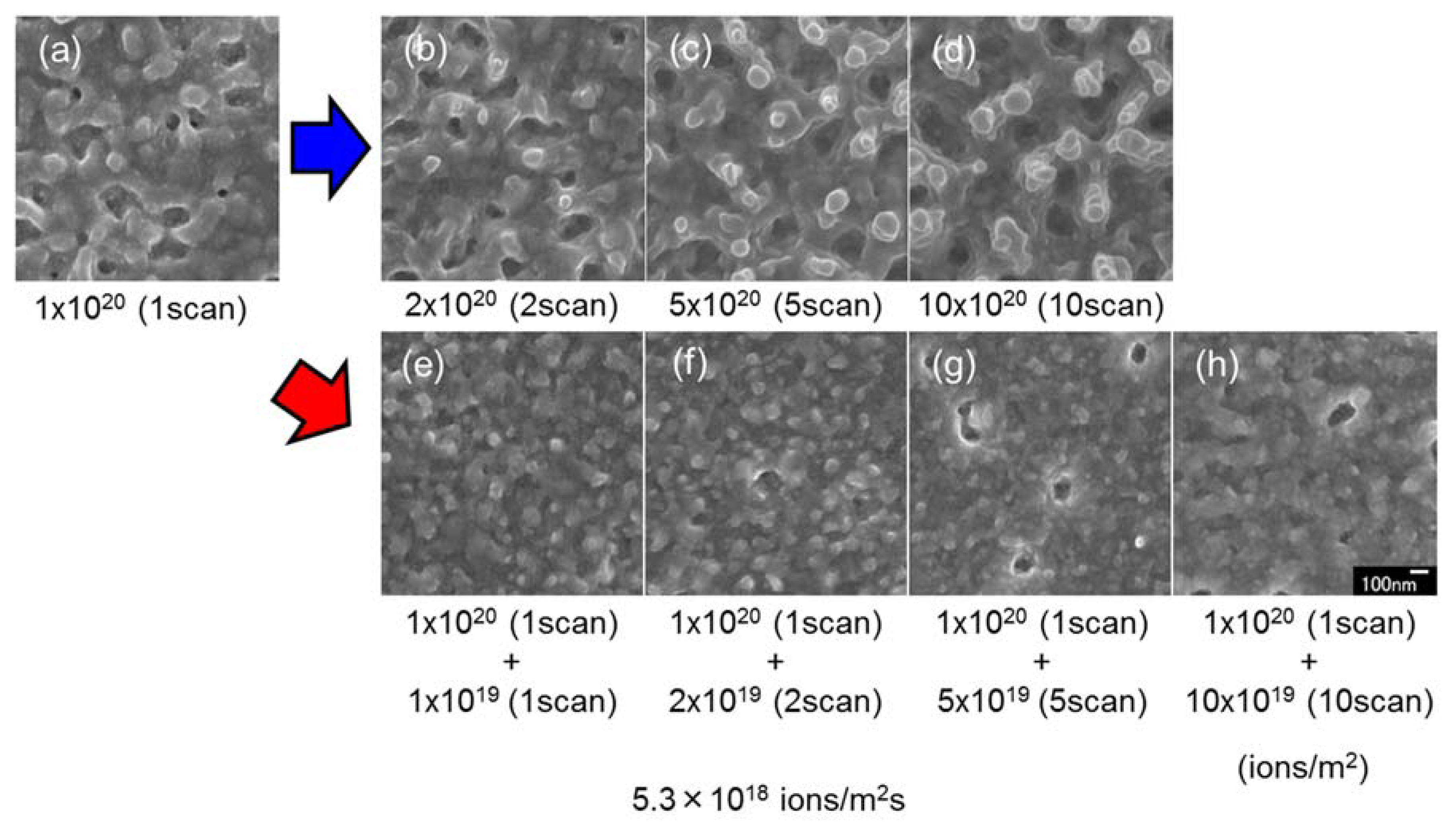
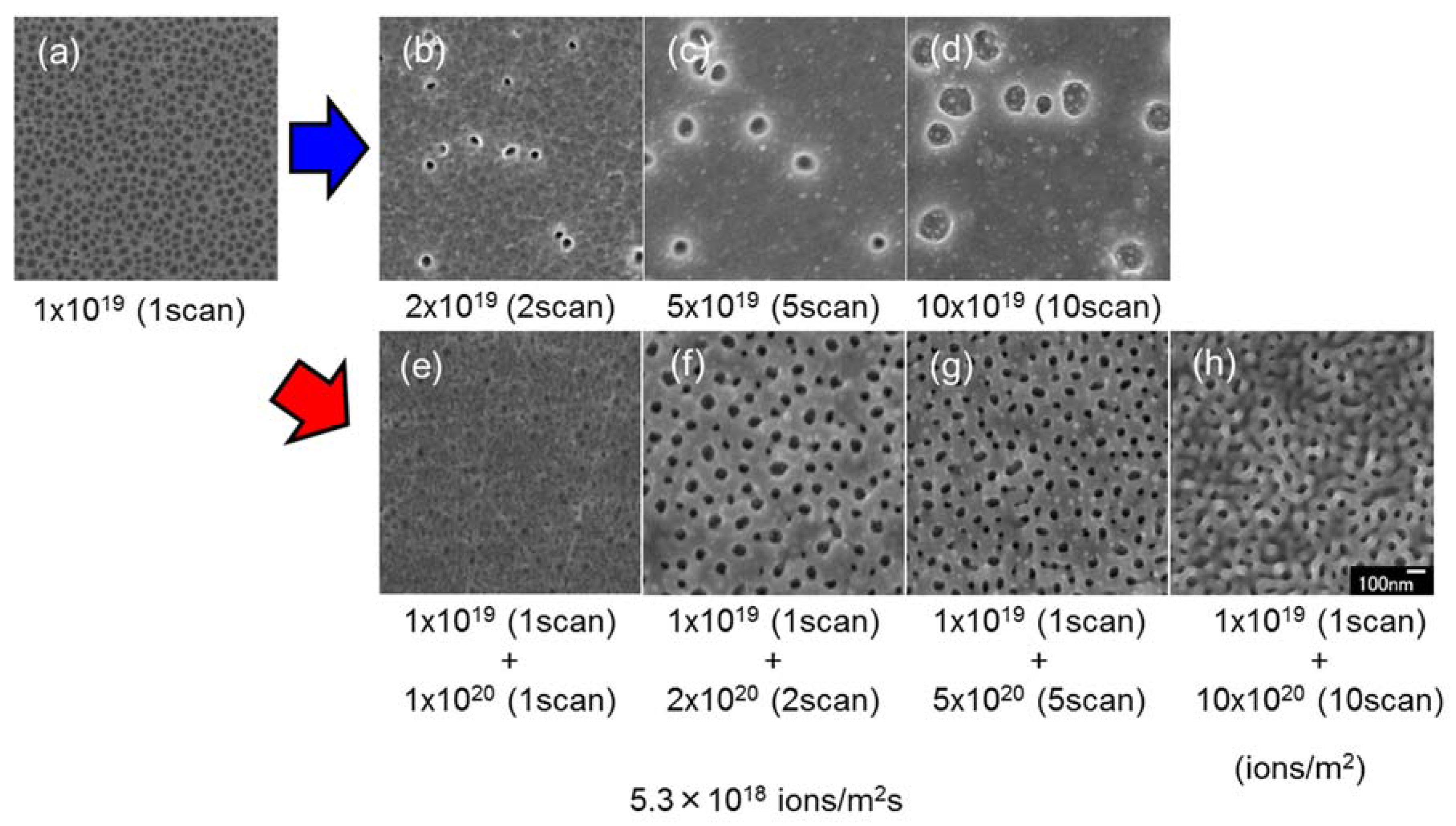
Figure 8 shows surface SEM images of InSb irradiated with two doses of a 30 kV Ga+ ion beam. The first and second irradiation doses were 1 × 10¹⁹ and 1 × 10²⁰ ions/m2 scan, respectively. The images shown in Figure 8a–d (reshown as Figure 2k–n) were collected after the first irradiation at a dose of 1 × 10¹⁹ ions/m2 scan, whereas those shown in Figure 8e–h were obtained after both irradiations (1 ×10¹⁹ and 1 × 10²⁰ ions/m2 scan). As shown in Figure 8a–h, the voids grew with increasing the ion dose, and the surface became rough. On the other hand, under superimposed irradiation, the void diameter was small. The small voids were observed in the sample depicted in Figure 8a, they did not grow larger by superimposed irradiation. The initial structure was important for the formation of the InSb structures. The induced interstitial migrated through the initial structure wall of void, resulting in the growth of voids.
Figure 9 shows surface SEM images of InSb with superimposed irradiation with a 30 kV Ga+ ion beam at a first irradiation dose of 1 × 10²⁰ ions/m2 scan (Figure 2p–s), and a second irradiation dose of 1 × 10¹⁹ ions/m2 scan. In contrast to the results shown in Figure 8, the first irradiation dose was high (1 × 10²⁰ ions/m2 scan), and the second irradiation dose was low (1 × 10¹⁹ ions/m2 scan). Pillar structures were observed on the sample surface after the first irradiation dose. Upon superimposed irradiation, pillars were not formed. This suggests that the mechanism of pillar formation was dominated by ion beam sputtering. The low-dose irradiation did not induce sputtering and void formation.
4. Conclusions
Ion beam conditions affected the formation of nanoporous structures on the InSb surface in this study. The structure’s size became large as the ion dose, flux (high-dose), and accelerating voltage increased. The structure’s shape changed from voids to pillars with increasing the ion dose. The oblique structure was obtained by tilting the sample by 45 degrees with respect to the ion beam radiation. Under the superposed ion beam irradiation, the structure’s shape was affected by the primary structure formed during the first irradiation dose in Figure 8 and Figure 9. The nanostructural features were easy to control by changing the conditions of ion beam irradiation.
Acknowledgments
We would like to thank Tomoya Oishi and Chiaki Watanabe, members of the nanoscience laboratory at the Kochi University of Technology, for SEM and FIB experiments.
Author Contributions
T.M. and N.N. conceived and designed the experiments; T.M. and N.N. performed the experiments; T.M. and N.N. analyzed the data; N.N. wrote the paper.
Conflicts of Interest
The authors declare no conflict of interest.
References
- Kleitman, D.; Yearian, H.J. Radiation-Induced Expansion of Semiconductors. Phys. Rev. 1957, 108, 901. [Google Scholar] [CrossRef]
- Destefanis, G.L.; Gailliard, J.P. Very efficient void formation in ion implanted InSb. Appl. Phys. Lett. 1980, 36, 40–42. [Google Scholar] [CrossRef]
- Gnaser, H.; Kallmayer, C.; Oechsner, H. Focused-ion-beam implantation of Ga in elemental and compound semiconductors. J. Vac. Sci. Tech. B 1995, 13, 19–26. [Google Scholar] [CrossRef]
- Kluth, S.M.; Llewellyn, D.; Ridgway, M.C. Irradiation fluence dependent microstructural evolution of porous InSb. Nucl. Instrum. Methods B 2006, 242, 640–642. [Google Scholar] [CrossRef]
- Perez-Bergqu, A.G.; Li, K.; Zhang, Y.; Wang, L.M. Ion irradiation-induced bimodal surface morphology changes in InSb. Nanotechnology 2010, 21, 325602. [Google Scholar] [CrossRef] [PubMed]
- Wu, J.H.; Goldman, R.S. Mechanisms of nanorod growth on focused-ion-beam-irradiated semiconductor surfaces: Role of redeposition. Appl. Phys. Lett. 2012, 100, 053103. [Google Scholar] [CrossRef]
- Kang, M.; Wu, J.H.; Ye, W.; Jiang, Y.; Robb, E.A.; Chen, C.; Goldman, R.S. Mechanisms of nanorod growth on focused-ion-beam-irradiated semiconductor surfaces: Role of redeposition. Appl. Phys. Lett. 2014, 104, 052103. [Google Scholar] [CrossRef]
- Datta, D.P.; Garg, S.K.; Satpati, B.; Sahoo, P.K.; Kanjilal, A.; Dhara, S.; Kanjilal, D.; Som, T. 60 keV Ar+-ion induced modification of microstructural, compositional, and vibrational properties of InSb. J. Appl. Phys. 2014, 116, 143502. [Google Scholar] [CrossRef]
- Jany, B.R.; Szajna, K.; Nikiel, M.; Wrana, D.; Trynkiewicz, E.; Pedrys, R.; Krok, F. Energy dependence of nanopillars formation on InSb semiconductor surfaces under gallium FIB and noble gas ions beam irradiation. Appl. Surf. Sci. 2015, 327, 86–92. [Google Scholar] [CrossRef]
- Homma, Y. Anomalous sputtering of gallium-antimonide under cesium-ionbombardment. J. Vac. Sci. Tech. A 1987, 5, 321–326. [Google Scholar] [CrossRef]
- Callec, R.; Favennce, P.N.; Salvi, M.; L’ Haridon, H.; Gauneau, M. Anomalous behavior of ion-implanted GaSb. Appl. Phys. Lett. 1991, 59, 1872–1874. [Google Scholar] [CrossRef]
- Facsko, S.; Dekorsy, T.; Koerdt, C.; Trappe, C.; Kurz, H.; Vogt, A.; Hartnagel, H.L. Formation of Ordered Nanoscale Semiconductor Dots by Ion Sputtering. Science 1999, 285, 1551–1553. [Google Scholar] [CrossRef] [PubMed]
- Nitta, N.; Taniwaki, M.; Hayashi, Y.; Yoshiie, T. Formation of cellular defect structure on GaSb ion-implanted at low temperatur. J. Appl. Phys. 2002, 92, 1799–1802. [Google Scholar] [CrossRef]
- Perez-Bergqu, A.G.; Zhu, S.; Sun, K.; Xiang, X.; Zhang, Y.; Wang, L.M. Embedded Nanofibers Induced by High-Energy Ion Irradiation of Bulk GaSb. Small 2008, 4, 1119–1124. [Google Scholar] [CrossRef] [PubMed]
- Nitta, N.; Hasegawa, T.; Yasuda, H.; Sato, K.; Xu, Q.; Yoshiie, T.; Taniwaki, M.; Hatta, A. Beam flux dependence of ion-irradiation-induced porous structures in III–V compound semiconductors. Radiat. Eff. Defect Solid 2013, 168, 247–252. [Google Scholar] [CrossRef]
- Datta, D.P.; Kanjilal, A.; Garg, S.K.; Sahoo, P.K.; Satpati, B.; Kanjilal, D.; Som, T. Controlled shape modification of embedded Au nanoparticles by 3MeV Au 2+-ion irradiation. Appl. Surf. Sci. 2014, 310, 189–195. [Google Scholar] [CrossRef]
- Kluth, P.; Sullivan, J.; Li, W.; Weed, R.; Schnohr, C.S.; Giulian, R.; Araujo, L.L.; Lei, W.; Rodriguez, M.D.; Afra, T.; et al. Nano-porosity in GaSb induced by swift heavy ion irradiation. Appl. Phys. Lett. 2014, 104, 023105. [Google Scholar] [CrossRef]
- El-Atwani, O.; Norris, S.A.; Ludwig, K.; Gonderman, S.; Allain, J.P. Ion beam nanopatterning of III-V semiconductors: consistency of experimental and simulation trends within a chemistry-driven theory. Sci. Rep. 2015, 5, 18207. [Google Scholar] [CrossRef] [PubMed]
- Wilson, H. The effects of self-ion bombardment (30–500 keV) on the surface topography of single-crystal germanium. J. Appl. Phys. 1982, 53, 1698–1705. [Google Scholar] [CrossRef]
- Appleton, B.R.; Holland, O.W.; Narayan, J.; Schow, O.E., III; Williams, J.S.; Short, K.T.; Lawson, E. Characterization of damage in ion implanted Ge. Appl. Phys. Lett. 1982, 41, 711–712. [Google Scholar] [CrossRef]
- Wang, L.M.; Birtcher, R.C. Radiation induced formation of cavities in amorphous germanium. Appl. Phys. Lett. 1989, 55, 2494–2496. [Google Scholar] [CrossRef]
- Wang, L.M.; Birtcher, R.C. Amorphization, morphological instability and crystallization of Krypton ion irradiated germanium. Philos. Mag. A 1991, 64, 1209–1223. [Google Scholar] [CrossRef]
- Koffel, S.; Scheiblin, P.; Claverie, A.; Benassayag, G. Amorphization kinetics of germanium during ion implantation. J. Appl. Phys. 2009, 105, 013528. [Google Scholar] [CrossRef]
- Steinbach, T.; Wernecke, J.; Kluth, P.; Ridgway, M.C.; Wesch, W. Structural modifications of low-energy heavy-ion irradiated germanium. Phys. Rev. B 2011, 84, 104108. [Google Scholar] [CrossRef]
- Romano, L.; Impellizzeri, G.; Bosco, L.; Ruffino, F.; Miritello, M.; Grimaldi, M.G. Nanoporosity induced by ion implantation in deposited amorphous Ge thin films. J. Appl. Phys. 2012, 111, 113515. [Google Scholar] [CrossRef]
- Impellizzeri, G.; Romano, L.; Bosco1, L.; Spinella, C.; Grimaldi, M.G. Nanoporosity induced by ion implantation in germanium thin films grown by molecular beam epitaxy. Appl. Phys. Express 2012, 5, 5035201. [Google Scholar] [CrossRef]
- Rudawski, N.G.; Darby, B.L.; Yates, B.R.; Jones1, K.S.; Elliman, R.G.; Volinsky, A.A. Nanostructured ion beam-modified Ge films for high capacity Li ion battery anodes. Appl. Phys. Lett. 2012, 100, 083111. [Google Scholar]
- Alkhaldi, H.S.; Kremer, F.; Bierschenk, T.; Hansen, J.L.; Nylandsted-Larsen, A.; Williams, J.S.; Ridgway, M.C. Porosity as a function of stoichiometry and implantation temperature in Ge/Si1−xGex alloys. J. Appl. Phys. 2016, 119, 094303. [Google Scholar] [CrossRef]
- Alkhaldi, H.S.; Kremer, F.; Mota-Santiago, P.; Nadzri, A.; Schauries, D.; Kirby, N.; Ridgway, M.C.; Kluth, P. Morphology of ion irradiation induced nano-porous structures in Ge and Si1−xGex alloys. J. Appl. Phys. 2017, 121, 115705. [Google Scholar] [CrossRef]
- Biersack, J.P.; Haggmark, L.G. A Monte Carlo computer program for the transport of energetic ions in amorphous targets. Nucl. Instrum. Methods 1980, 174, 257. [Google Scholar] [CrossRef]
- Ziegler, J. Software web site. Available online: http://www.SRIM.org (accessed on 10 July 2017).
- Bauerlein, R.Z. Messung der Energie zur Verlagerung eines Gitteratoms durch Elektronenstoß in AIIIBV-Verbindungen. Physics 1963, 176, 498–509. [Google Scholar] [CrossRef]
Figure 1.
Surface scanning electron microscopy (SEM) images of indium antimonide (InSb) irradiated with a 30 kV Ga+ ion beam at different doses of (a–e) 1 × 10¹⁷ ions/m2 scan, (f–j) 1 × 10¹⁸ ions/m2 scan, (k–o) 1 × 10¹⁹ ions/m2 scan, and (p–t) 1 × 10¹⁹ ions/m2 scan, and different low fluxes of (a–e) 2.0 × 10¹⁸ ions/m2 s, (f–j) 1.5 × 10¹⁸ ions/m2 s, (k–o) 1.6 × 10¹⁸ ions/m2 s, and (p–t) 1.5 × 10¹⁸ ions/m2 s, at room temperature.
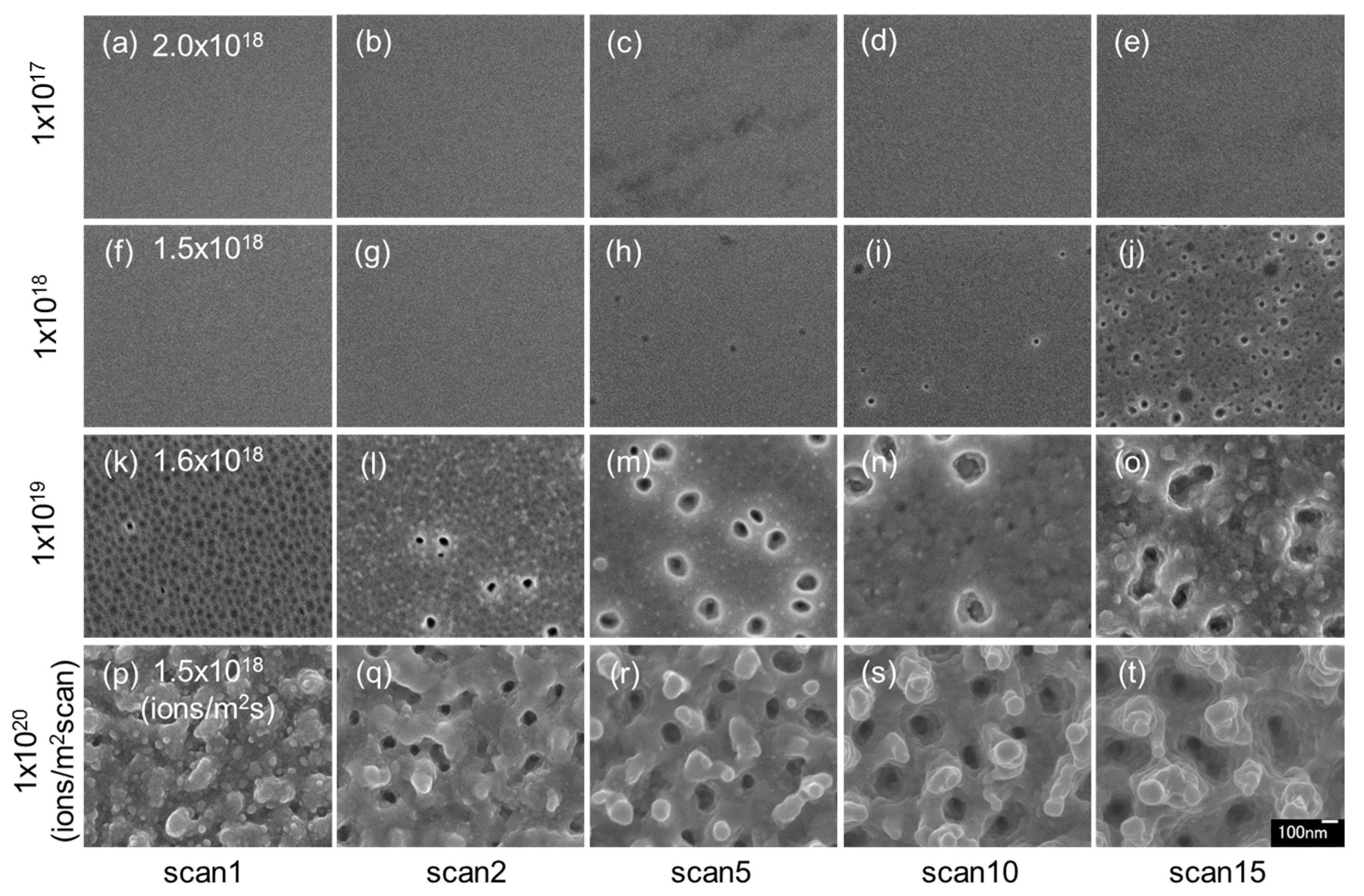
Figure 2.
Surface SEM images of InSb irradiated with a 30 kV Ga+ ion beam at different doses of (a–e) 1 × 10¹⁷ ions/m2 scan, (f–j) 1 × 10¹⁸ ions/m2 scan, (k–o) 1 × 10¹⁹ ions/m2 scan, and (p–t) 1 × 10¹⁹ ions/m2 scan, and different high fluxes of (a–e) 6.9 × 10¹⁸ ions/m2 s, (f–j) 5.1 × 10¹⁸ ions/m2 s, (k–o) 5.3 × 10¹⁸ ions/m2 s, and (p–t) 5.3 × 10¹⁸ ions/m2 s, at room temperature.
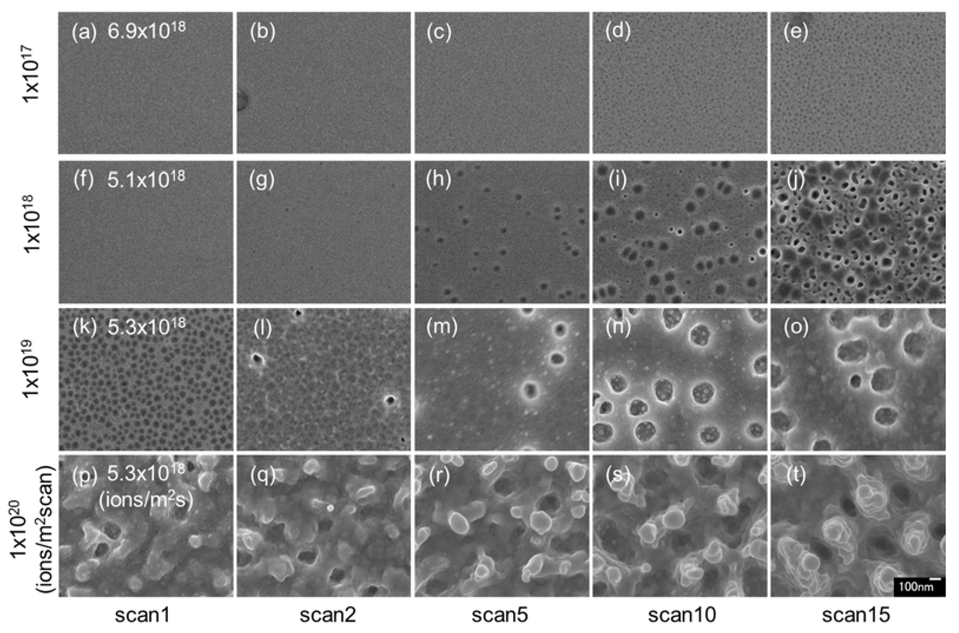
Figure 3.
Diameters of the void structures on the InSb samples shown in Figure 1 and Figure 2 as a function of irradiation dose.
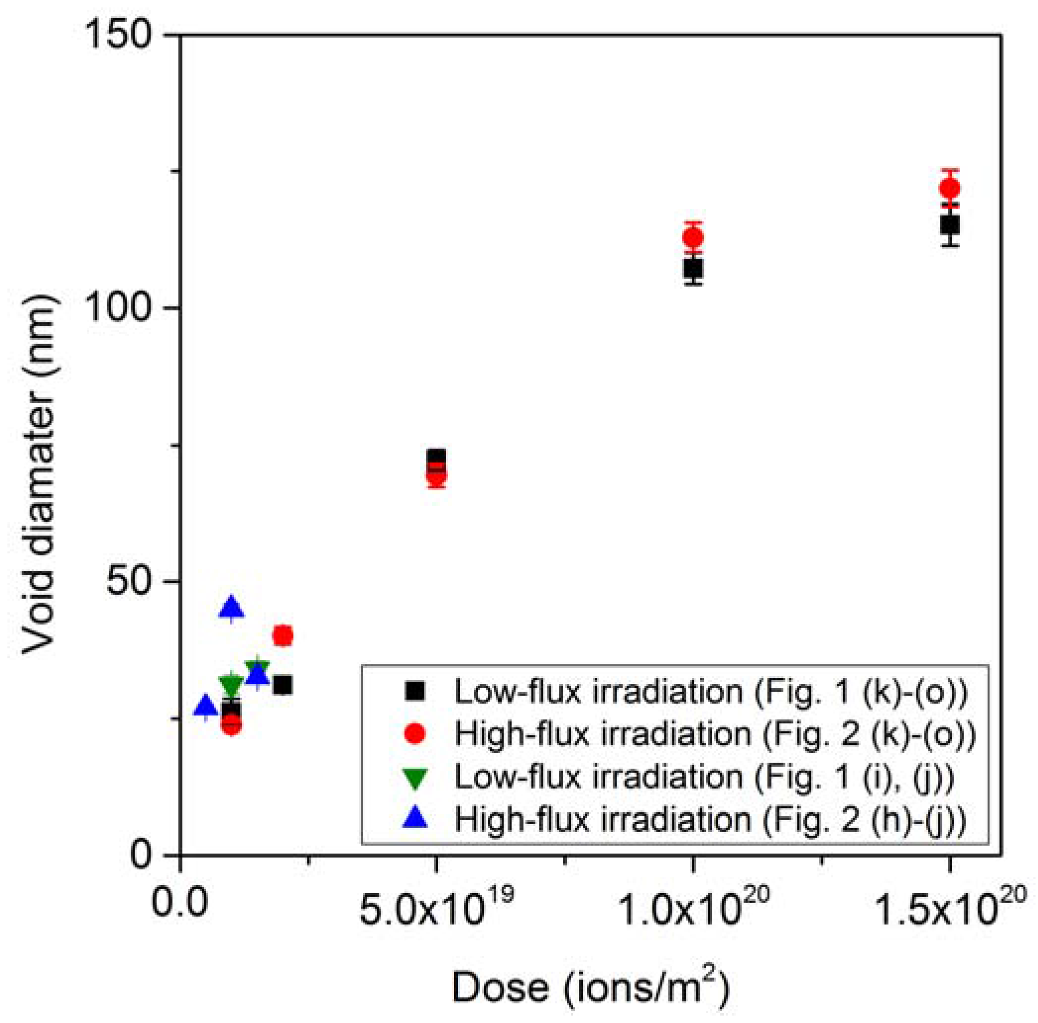
Figure 4.
Surface SEM images of InSb irradiated with a 30 kV Ga+ ion beam at a dose of 1 × 10²⁰ ions/m2 scan, fluxes of (a–e) 1.5 × 10¹⁸ ions/m2 s (low-flux irradiation (reshown as Figure 1p–t)), (f–j) 5.3 × 10¹⁸ ions/m2 s (high-flux irradiation (reshown as Figure 2p–t)), and (k–o) 2.7 × 10¹⁹ ions/m2 s (highest-flux irradiation), at room temperature.
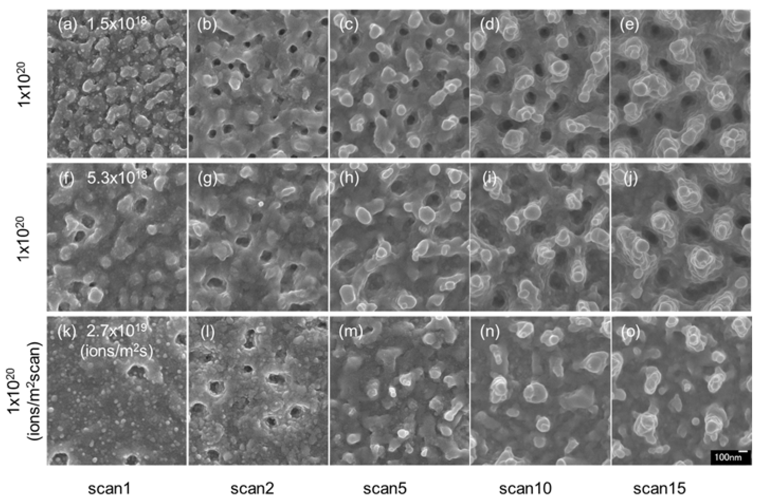
Figure 5.
Surface SEM images of InSb irradiated with Ga+ ion beams at a dose of 1 × 10²⁰ ions/m2 scan, fluxes (highest-flux irradiation) of (a–e) 2.9 × 10¹⁹ ions/m2 s and (f–j) 2.7 × 10¹⁹ ions/m2 s, accelerating voltages of (a–e) 16 kV and (f–j) 30 kV (reshown as Figure 4k–o), at room temperature.
Figure 5.
Surface SEM images of InSb irradiated with Ga+ ion beams at a dose of 1 × 10²⁰ ions/m2 scan, fluxes (highest-flux irradiation) of (a–e) 2.9 × 10¹⁹ ions/m2 s and (f–j) 2.7 × 10¹⁹ ions/m2 s, accelerating voltages of (a–e) 16 kV and (f–j) 30 kV (reshown as Figure 4k–o), at room temperature.
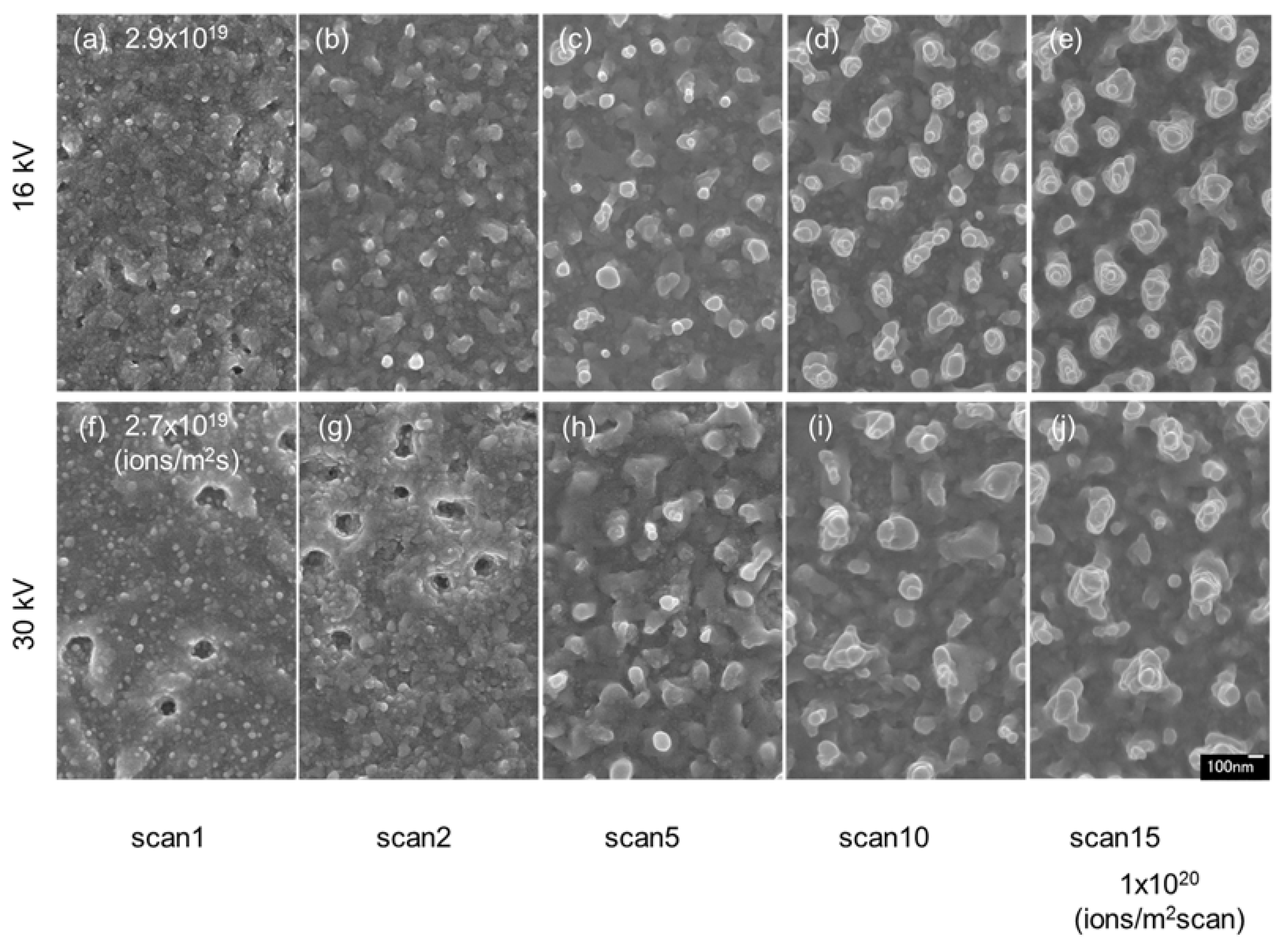
Figure 6.
Surface SEM images of InSb irradiated with a 30 kV Ga+ ion beam at a dose of 1 × 10²⁰ ions/m2, fluxes of (a–j) 5.1 × 10¹⁸ ions/m2 s, (k–o) 5.3 × 10¹⁸ ions/m2 s, and (p–t) 5.4 × 10¹⁸ ions/m2 s (high-flux irradiation), irradiation angles of (a–e) (reshown as Figure 2f–j) and (k–o) 0° (reshown as Figure 2p–t) and (f–j) and (p–t) 45°, at room temperature.
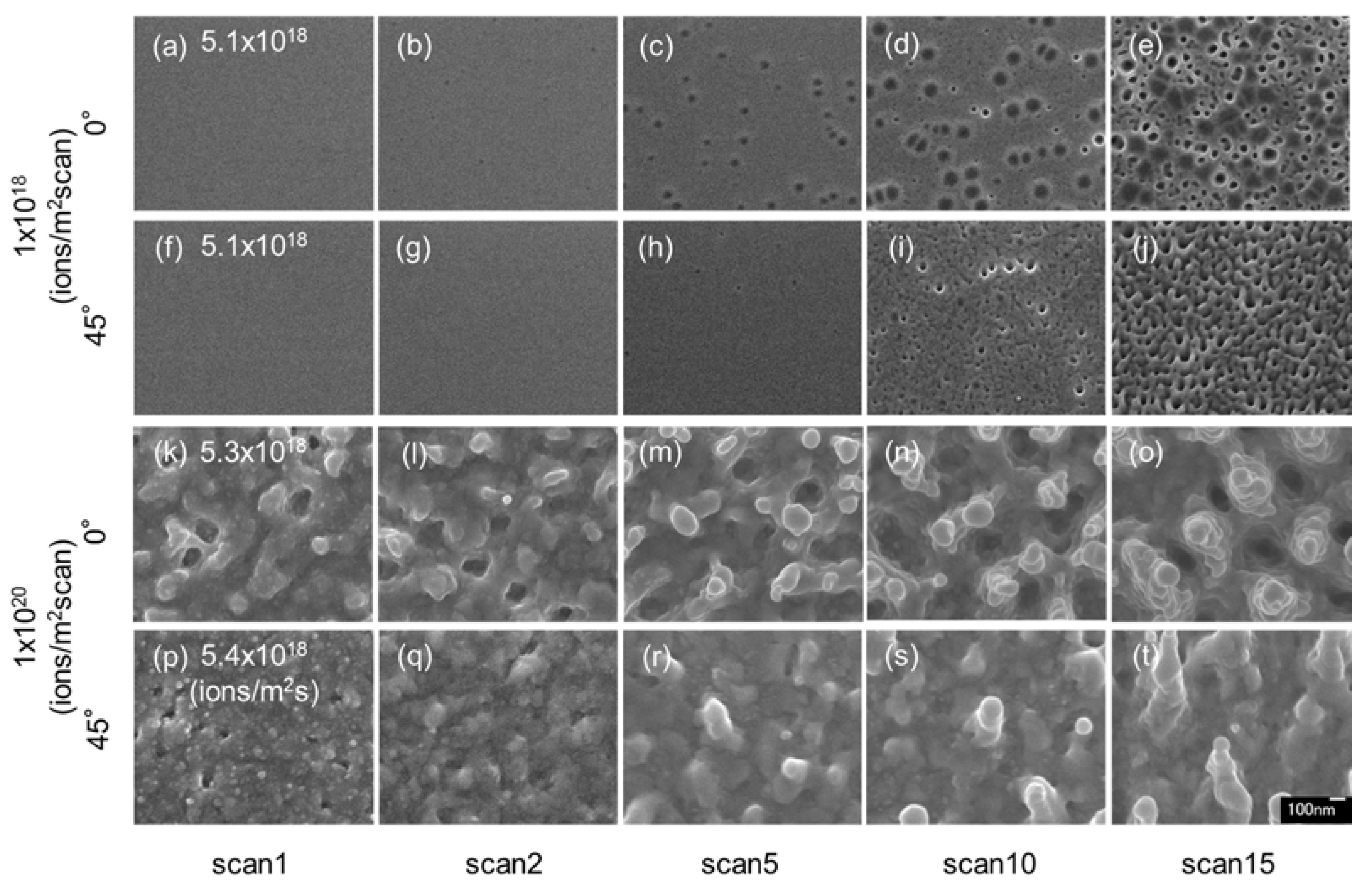
Figure 7.
Energy-dispersive X-ray spectroscopy (EDX) maps of InSb irradiated with a 30 kV Ga+ ion beam at a dose of 3 × 10²⁰ ions/m2, and a flux of 5.3 × 10¹⁸ ions/m2 s, at room temperature.
Figure 7.
Energy-dispersive X-ray spectroscopy (EDX) maps of InSb irradiated with a 30 kV Ga+ ion beam at a dose of 3 × 10²⁰ ions/m2, and a flux of 5.3 × 10¹⁸ ions/m2 s, at room temperature.
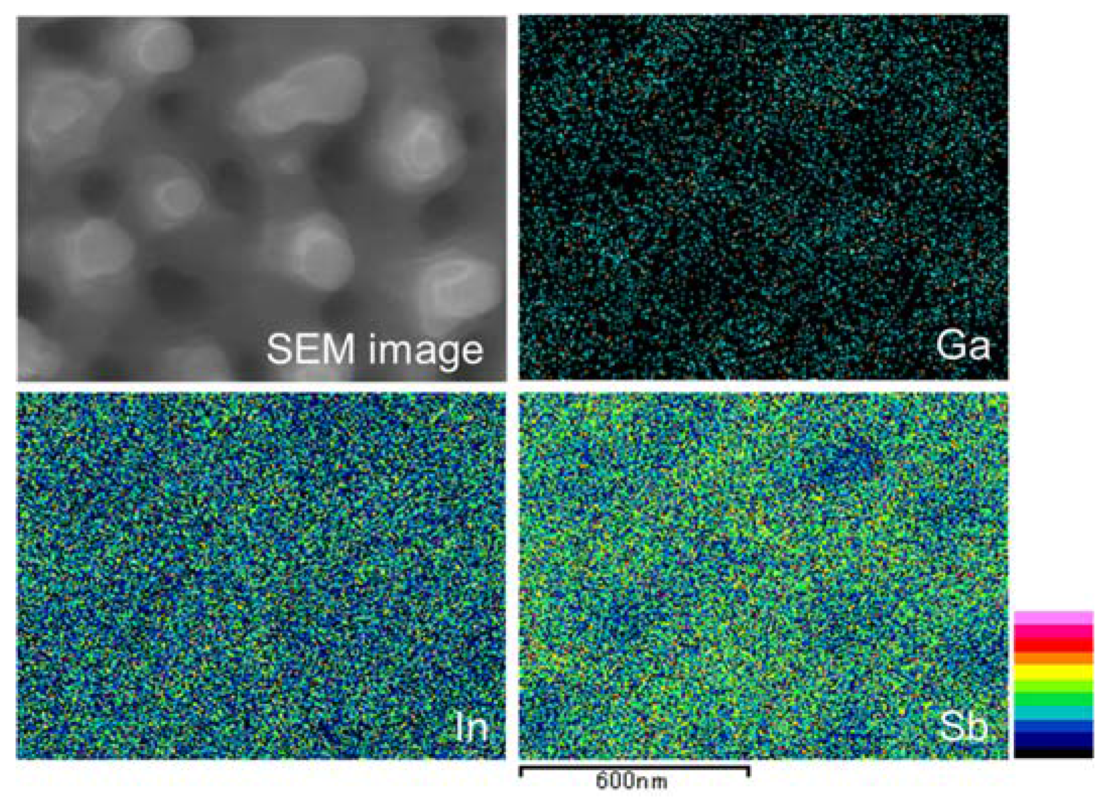
Figure 8.
Surface SEM images of InSb irradiated with a 30 kV Ga+ ion beam at doses of (a) 1 × 10¹⁹ ions/m2 (1 scan), (b) 2 × 10¹⁹ ions/m2 (2 scan), (c) 5 × 10¹⁹ ions/m2 (5 scan), (d) 10 × 1019 ions/m2 (10 scan) (re-shown as Figure 2k–n), (e) 1 × 10¹⁹ ions/m2 (1 scan) + 1 × 10²⁰ ions/m2 (1 scan), (f) 1 × 10¹⁹ ions/m2 (1 scan) + 2 × 10²⁰ ions/m2 (2 scans) , (g) 1 × 10¹⁹ ions/m2 (1 scan) + 5 × 10²⁰ ions/m2 (5 scans), and (h) 1 × 10¹⁹ ions/m2 (1 scan) + 10 × 1020 ions/m2 (10 scans), at a flux of 5.3 × 10¹⁸ ions/m2 s, at room temperature.

Figure 9.
Surface SEM images of InSb irradiated with a 30 kV Ga+ ion beam at doses of (a) 1 × 10²⁰ ions/m2 (1 scan), (b) 2 × 10²⁰ ions/m2 (2 scan), (c) 5 × 10²⁰ ions/m2 (5 scans), (d) 10 × 1020 ions/m2 (10 scans) (reshown as Figure 2p–s), (e) 1 × 10²⁰ ions/m2 (1 scan) + 1 × 10¹⁹ ions/m2 (1 scan), (f) 1 × 10²⁰ ions/m2 (1 scan) + 2 ×10¹⁹ ions/m2 (2 scans), (g) 1 × 10²⁰ ions/m2 (1 scan) + 5 × 10¹⁹ ions/m2 (5 scans), and (h) 1 × 10²⁰ ions/m2 (1 scan) + 10 × 1019 ions/m2 (10 scans), at a flux of 5.3 × 10¹⁸ ions/m2 s, at room temperature.

Table 1.
Sputtering yield (atoms per ion) of In and Sb on indium antimonide (InSb) irradiated with Ga+ ions calculated by stopping and range of ions in matter (SRIM) simulation.
Table 1.
Sputtering yield (atoms per ion) of In and Sb on indium antimonide (InSb) irradiated with Ga+ ions calculated by stopping and range of ions in matter (SRIM) simulation.
| Sputtering Yield (Atoms/Ion) | |||
|---|---|---|---|
| Accelerating Voltage | 16 kV | 30 kV | 30 kV (45°) |
| Total | 7.975 | 8.537 | 14.698 |
| In | 4.19 | 4.47 | 7.68 |
| Sb | 3.78 | 4.07 | 7.02 |
Table 2.
EDX quantification (atomic %) of InSb irradiated with a 30 kV Ga+ ion beam at a dose of 3 × 10²⁰ ions/m2, and a flux of 5.3 × 10¹⁸ ions/m2 s, at room temperature.
Table 2.
EDX quantification (atomic %) of InSb irradiated with a 30 kV Ga+ ion beam at a dose of 3 × 10²⁰ ions/m2, and a flux of 5.3 × 10¹⁸ ions/m2 s, at room temperature.
| EDX Quantification (Atomic %) | |
|---|---|
| Ga | 3.5 |
| In | 52 |
| Sb | 45 |
© 2017 by the authors. Licensee MDPI, Basel, Switzerland. This article is an open access article distributed under the terms and conditions of the Creative Commons Attribution (CC BY) license (http://creativecommons.org/licenses/by/4.0/).
Share and Cite
MDPI and ACS Style
Miyaji, T.; Nitta, N. Nanoporous Structure Formation on the Surface of InSb by Ion Beam Irradiation. Nanomaterials 2017, 7, 204. https://doi.org/10.3390/nano7080204
AMA Style
Miyaji T, Nitta N. Nanoporous Structure Formation on the Surface of InSb by Ion Beam Irradiation. Nanomaterials. 2017; 7(8):204. https://doi.org/10.3390/nano7080204
Chicago/Turabian StyleMiyaji, Takashi, and Noriko Nitta. 2017. "Nanoporous Structure Formation on the Surface of InSb by Ion Beam Irradiation" Nanomaterials 7, no. 8: 204. https://doi.org/10.3390/nano7080204
Note that from the first issue of 2016, this journal uses article numbers instead of page numbers. See further details here.