
One-Dimensional Electron Transport Layers for Perovskite Solar Cells


1
Department of Electrical and Computer Engineering, University of Alberta, Edmonton, AB T6G 1H9, Canada
2
National Research Council, National Institute for Nanotechnology, 11421 Saskatchewan Drive NW, Edmonton, AB T6G 2M9, Canada
*
Author to whom correspondence should be addressed.
†
These authors contributed equally.
Nanomaterials 2017, 7(5), 95; https://doi.org/10.3390/nano7050095
Submission received: 12 February 2017
/
Revised: 3 April 2017
/
Accepted: 24 April 2017
/
Published: 29 April 2017
(This article belongs to the Special Issue New Developments in Nanomaterials for Energy Storage and Conversions)
Abstract
:The electron diffusion length (Ln) is smaller than the hole diffusion length (Lp) in many halide perovskite semiconductors meaning that the use of ordered one-dimensional (1D) structures such as nanowires (NWs) and nanotubes (NTs) as electron transport layers (ETLs) is a promising method of achieving high performance halide perovskite solar cells (HPSCs). ETLs consisting of oriented and aligned NWs and NTs offer the potential not merely for improved directional charge transport but also for the enhanced absorption of incoming light and thermodynamically efficient management of photogenerated carrier populations. The ordered architecture of NW/NT arrays affords superior infiltration of a deposited material making them ideal for use in HPSCs. Photoconversion efficiencies (PCEs) as high as 18% have been demonstrated for HPSCs using 1D ETLs. Despite the advantages of 1D ETLs, there are still challenges that need to be overcome to achieve even higher PCEs, such as better methods to eliminate or passivate surface traps, improved understanding of the hetero-interface and optimization of the morphology (i.e., length, diameter, and spacing of NWs/NTs). This review introduces the general considerations of ETLs for HPSCs, deposition techniques used, and the current research and challenges in the field of 1D ETLs for perovskite solar cells.
1. Introduction
The increasing global demand for energy has spurred research efforts to find new and improved sources of cheap, environmentally neutral, renewable energy. Inorganic solar cells based on materials such as crystalline silicon, cadmium telluride, or copper indium germanium selenide (CIGS) constitute mature technologies that exhibit a relatively high power conversion efficiency (PCE) of around 12%–20% in deployed modules [1] and thus dominate commercially available photovoltaic technologies. However, the relatively long energy payback times of inorganic solar cells [2,3] have partially impeded their pace to widespread deployment, and thus alternative approaches are being explored. Organic photovoltaics [4], dye-sensitized solar cells [5], halide perovskite solar cells [6], and quantum-dot solar cells [7] are examples of next generation solution-processable solar cell technologies that have emerged as lower cost, lower energy payback time alternatives to replace conventional solar cells [8,9]. Among these technologies, halide perovskite solar cells (HPSCs) are currently the topic of intense scientific and engineering interest due to their facile synthesis, use of earth-abundant constituent elements and high device performance [10]. A major breakthrough occurred in 2012 when Snaith et al. [11] reported an HPSC device with a PCE of 11% using a mixed halide perovskite layer (CH3NH3PbI3−xClx) as the active layer on nanoporous aluminum oxide. The first report of a HPSC was by Miyasaka and co-workers, who obtained a PCE of 3.8% in 2009 [12] using an active layer consisting of CH3NH3PbI3 (henceforth referred to as MAPbI3).
Perovskites, named after the Russian mineralogist Lev A. Perovski, are compounds having the molecular formula ABX3 and a specific crystal structure consisting of A and B cations together with X anions arranged in a cubic array of BX6 octahedra sharing corners, with the A cations placed in the cuboctahedral interstices which belong to the cubic Pm3m crystal structure as shown in Figure 1 [13]. In halide perovskites, X is a halide ion while A is a monovalent ion such as Cs+, CH3NH3+ (MA), or NH=CHNH3+, and B is a divalent ion such as Pb2+ or Sn2+. Unlike oxide perovskites, halide perovskites are not strictly ionic since the bond between the Group IV metal atom and the halide atom has some covalent character, which is maximum for iodide perovskites.
Halide perovskites have unique properties [15] such as a direct optical bandgap, broadband light absorption, low carrier effective masses, dominant shallow point defects, benign grain boundaries, ambipolar transport, and long carrier diffusion lengths, due to which they have been investigated as light-absorbing and charge transporting materials in photovoltaic devices. In an astonishingly short period, this has led to an as-of-yet highest power conversion efficiency of 21.1% [16]. The highest efficiencies reported thus far, have been obtained using iodide perovskites, and mixed iodide-bromide perovskites. One challenge associated with perovskite solar cells is the choice of electron transport layer (ETL) in the solar cell architecture. It is important for the ETL to possess certain properties including an appropriate work function, high conductivity, fast charge transport, and a low recombination rate at the interface. Both inorganic and organic semiconductors have been used, with TiO2 being the most commonly used and having seen the most success. The morphology of the ETL layer is also of importance with planar film layers, mesoscopic particulate layers, and nanostructured layers being used. Planar film layers, while being the easiest to fabricate, are required to have a sufficient thickness in order to absorb all of the incident solar light. This thickness, however, is usually required to be longer than the diffusion length of electrons, which has been measured to be 100 nm or higher in iodide perovskites [17]. Mesoscopic electron transport layers have the advantage of allowing for infiltration of the perovskite, meaning that any dimension of the perovskite is kept to a minimum while still being able to absorb all the sun’s incident light [18]. However, it can be very difficult to completely fill the pore network of a mesoscopic structure with perovskite, and any unfilled areas inevitably lead to recombination at the exposed surfaces. In addition, a mesoscopic structure consisting of an interconnected network of nanoparticles, results in non-directional electron transport involving a random walk [19]. One dimensional nanostructures (1D-NS), however, are able to lever the same advantages of mesoscopic structures, while being able to allow for a more complete infiltration of perovskite into the electron transporting layer. Furthermore, their directional charge transport properties enable increased solar cell efficiencies [20,21,22,23]. In addition, 1D-NS with optimized geometries enable the improved management of incident photons in the solar cell. This review aims to summarize the fundamentals of preparing perovskite solar cells and how they relate to using one-dimensional electron transport layers (1D-ETLs), with emphasis on TiO2 and ZnO nanostructures as the leading candidates. The fundamentals of selecting and fabricating ETLs will be discussed, as well as the special considerations that one has to take into account when dealing with one-dimensional nanostructures. Finally, issues that still need to be solved in order for 1D-NS to achieve commercial viability are addressed.
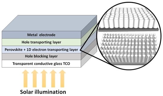
2. Architecture and Working Mechanism of Devices
As shown in Figure 2, perovskite solar cells are fabricated in two major architectures, p-i-n and n-i-p type. In the p-i-n type architecture, a p-type hole transporting layer (HTL) such as CuO, NiO or PEDOT: PSS is deposited on a transparent conductive oxide (TCO) coated glass substrate namely fluorine doped tin oxide (FTO) or indium tin oxide (ITO) coated glasses. This is followed by the deposition of the perovskite active layer which is then coated over by a n-type film of [6,6]-phenyl-C61-butyric acid methyl ester (PCBM), ZnO, or C60 which acts as an ETL and subsequently a low work-function metal such as aluminum is evaporated to complete the device [24,25,26,27,28,29]. In the n-i-p type architecture, an n-type ETL such as TiO2, ZnO, SnO2 or WO3 is deposited on a TCO-coated glass substrate which is then followed by perovskite deposition. Over the perovskite, a p-type hole transporting layer (typically spiro-MeOTAD) is deposited and finally a high work function metal such as gold is deposited to complete the device [30,31,32,33,34,35,36,37,38]. This n-i-p configuration is necessarily used for the formation of solar cells involving 1D-ETLs to allow for proper infiltration of the perovskite into the ETL. Also of note is that ETL-free and HTL-free perovskite solar cells do exist but their photovoltaic performance is low [33,39].
3. Halide Perovskite Deposition Techniques
The performance of perovskite solar cells is highly dependent on the crystal structure and morphology of the perovskite absorber, as well as the degree of contact the perovskite makes with the charge transport layers. These factors vary significantly in accordance with the deposition procedure, which should ensure good infiltration and contact when dealing with 1D-ETLs. Furthermore, to prevent direct contact between the electron transporting layer and hole transporting layer, an optimum thickness of perovskite overlayer is needed. This overlayer helps to ensure a sufficiently high value for the shunt resistance. Typically, single step spin coating, two step spin coating, and sequential deposition techniques are used to deposit the active layer in perovskite solar cells. Figure 3a is a block diagram of the one step spin casting method which involves the mixing of AX and BX2 in polar solvents such as γ-butyrolactone (GBL), dimethylformamide (DMF) and dimethyl sulfoxide (DMSO) to make the perovskite precursor solution. Spin casting of the precursor solution at sufficient revolutions per minute (RPM) is used to achieve the desired film thickness. This technique generally involves two spinning steps—one at low RPM and another at high RPM. In a typical synthesis, toluene or chlorobenzene is added to the spinning substrate prior to the completion of the second spinning step. After the spin coating step, the substrates are annealed in order to force the crystallization of the deposited perovskite layer. This procedure for perovskite active layer deposition was initially introduced by Miyasaka and coworkers in 2009 and perovskite solar cells with the highest PCEs reported to date employ this technique [12].
Figure 3b illustrates the methodology of the sequential deposition technique in which BX2 is dissolved in polar solvents such as DMF and DMSO while another solution of AX is made in 2-propanol. First, BX2 is spin coated over the substrate followed by calcination. After cooling down the substrate to room temperature, it is dipped into AX solution followed by annealing to crystallize the perovskite. The sequential deposition procedure was initially developed by Mitzi and colleagues in 1998 [44] while Gratzel et al. re-introduced this technique to fabricate perovskite solar cells in 2013 [45]. A major problem with this methodology is the length of time needed to convert BX2 into ABX3, during which some of the formed ABX3 can be leached away from the substrate. Two-step spin coating, illustrated in Figure 3c, is a modified version of sequential deposition in which BX2 is first spin coated over the substrate followed by calcination. After cooling down the substrate to room temperature AX dissolved in 2-propanol is spin coated over the dry BX2 layer. Another important deposition technique that has the ability to produce high performance perovskite solar cells is the dual source vapor deposition technique which was reported in 2013 by Snaith et al. [40]. As shown in Figure 3d, AX and BX2 are evaporated simultaneously from two different sources in a particular evaporation ratio to form ABX3 film on substrate which is then annealed. Other deposition techniques include sequential vacuum deposition [46], chemical vapor deposition [47], inkjet printing [48,49], spray coating [50,51], and slot die coating [52], but these methods have not been successful thus far in producing high efficiency photovoltaic devices.
4. One Dimensional Nanostructures
1D-NS used in photovoltaics, taking the form of familiar structures such as rods, tubes, and wires, possess two dimensions of a size between 1 and 100 nm while the third dimension is typically in the range 200 nm–1 μm. A wide variety of top-down and bottom-up fabrication approaches exist for their synthesis, with varying degrees of complexity that allow for greater or lesser control over the final structure. Chemical synthesis strategies for 1D-NS are often the cheapest and least demanding in terms of deposition equipment, and include electrodeposition, sol–gel synthesis, solvothermal methods, and electrochemical anodization. While ease of fabrication and relatively high-throughput make these methods attractive options, they often suffer from the drawback of having a greater variability in final properties due to the indirect measures of control inherent to these methods. Strategies based on physical or physicochemical synthesis of 1D-NS such as vapor phase deposition, chemical vapor deposition, vapor-liquid-solid growth, and atomic layer deposition often result in superior electronic properties due to lower impurities and superior crystallinity while requiring dedicated deposition equipment and extreme conditions such as high vacuum and/or elevated temperatures. Even more precise control over the final structure can be obtained by techniques such as electron beam lithography or focused-ion beam writing or x-ray lithography, although these processes are much more expensive and of low-throughput.
Several studies have found that the diffusion length of photogenerated electrons in halide perovskites is lower than that of photogenerated holes as shown in Figure 4, which calls for the application of nanostructured ETLs in perovskite solar cells [53,54]. 1D-NS offer a large surface area and the possibility of confinement of phonons and charge carriers, which leads to distinct electrical, optical and structural properties when contrasted with those of bulk materials. They may be used to limit the “random walk” of charges through a material; as there is only one direction in which charges may travel, the overall length of the path a charge takes on its way to being collected is reduced and thus charge recombination is limited. It is also important to use an optimized thickness of ETLs in perovskite solar cells (corresponding to the length of 1D ETL nanostructures). Because most perovskite semiconductors used in solar cells have a high extinction coefficient, an increase in the thickness of 1D ETLs does not generally improve the overall absorption of the device. However, increasing the thickness of 1D ETLs can reduce the photovoltaic performance of perovskite solar cells. The open circuit voltage decreases as the nanostructure length increases because of increased recombination at the ETL/perovskite interface [55,56,57]. The short circuit current too typically decreases because of ultraviolet photons absorbed by thicker ETLs which cannot be transmitted to the perovskite absorber layer [55,58]. The fill factor also reduces because of an increased series resistance of the solar cell. On the other hand, too thin an ETL does not provide a sufficient mesoscopic effect. If left unoptimized, forward- and back-scattering due to thick nanostructured ETLs can outcouple incident photons out of the device and reduce the amount of light harvested [59]. The nanorod packing density in 1D ETLs is another important parameter which plays a crucial role in the photovoltaic performance of solar cells. If the nanorods are densely packed, then there is less room between adjacent nanorods/nanotubes for the perovskite to be filled, resulting in poor filling and lower photovoltaic performance of the solar cells. Moderate and low density packing of the nanorods constituting the 1D ETL provide better filling and thus improved light harvesting efficiency [60,61,62]. Thus, it is important to optimize the thickness and morphology of 1D ETLs to take proper advantage of their directional charge transport and light management properties without harming other performance parameters of the solar cell. For high aspect ratio nanorods in the ETL, field emission of electrons into the perovskite is promoted, which in turn, may increase the dark current in the solar cells and thereby reduce the Voc value [59]. A superficial coating of perovskite is favored for high aspect ratio NRs with polar surfaces due to wetting considerations, as opposed to volumetric filling of the inter-rod spaces, which can exacerbate problems with extracting holes.
5. Materials for One Dimensional Electron Transport Layers
Both inorganic and organic semiconductors have been used as electron transport materials, although it is inorganic materials that have received attention for their applicability as one-dimensional nanostructures since the morphological integrity of organic semiconductor nanostructures typically does not survive the subsequent solution deposition of the halide perovskite due to the partial or complete solubility of the organic semiconductors in solvents such as GBL, DMF, and DMSO [63,64]. It is worth noting, however, that research efforts towards the development of one-dimensional organic semiconductors are being made through techniques such as solution-phase synthesis, templating, electrospinning, and nanolithography [65]. TiO2, ZnO, SnO2, and WOx are the most commonly used materials (energy level diagram shown in Figure 5) for 1D-ETLs, although other inorganic semiconductors exist that could potentially be used in a one-dimensional nanostructure, such as Zn2SnO4 [66], BaSnO3 [67], and SrTiO3 [68]. While not a focus of this review, common organic electron transport materials include fullerenes, methanofullerenes, and perylene derivatives. There are several major considerations when selecting the material to use as ETL, including the energy level alignment with respect to the particular perovskite absorber used, the doping density, the density and energetic depth of trap states in the material, the electron mobility, and hole blocking action. The material most commonly used as the ETL is TiO2, which exhibits good electron transporting properties and is known to be non-toxic and chemically stable. TiO2 exists in three crystalline phases—anatase, brookite, and rutile [69], among which the anatase phase TiO2 has been used the most widely and achieved the highest performance in photovoltaic applications due to possessing a higher effective surface area, faster electron transport, and longer electron lifetime than the other two phases [70,71]. The anatase phase of TiO2 also exhibits exceptional hole blocking, which is highly desirable. However, a major issue with TiO2 and its potential to be used in commercial applications, is the high temperature processing typically required to anneal the TiO2 into these crystalline forms, since the as-fabricated TiO2, is often amorphous. In light of this problem, efforts have been made to develop crystalline TiO2 without the need for high-temperature processes [72]. Compared to other candidate ETL materials, TiO2 possesses a high density of shallow- and deep-trapping states [73] that in turn promote Shockley-Read-Hall type recombination and Fermi-level pinning at interfaces with other materials. The most widely investigated replacement for TiO2 is ZnO, which has a 5–10 fold higher electron mobility [74] and suitable energy levels. However, processing issues and the poorer chemical stability of ZnO have hindered the use and development of ZnO as an ETL. SnO2 has an electron mobility nearly two orders of magnitude higher than that of TiO2 [75], yet shows much lower PCEs due to non-optimal energy levels and high recombination rates. Similarly, WOx has exhibited poor performance when used by itself. However, both SnO2 and WOx have shown increased performance when used in combination with ZnO and TiO2, such as in a core shell structure [38]. Such a core-shell structure can effectively suppress recombination and improve the electron transfer at the ETL/perovskite interface, resulting in improved solar cell performance [61,76].
6. Classes of One Dimensional Nanostructures Used as ETLs in Perovskite Solar Cells
The vast majority of 1D-ETLs take the form of nanotubes or nanorods (also known as nanowires). However, other morphologies do exist, including nanofibers and core-shell structures utilizing two or more materials as the electron transporting layer. Herein, we focus on the structure and function of TiO2 nanotubes, TiO2 nanorods, and ZnO nanorods, with the reported solar cell performance of TiO2 1D-ETLs and ZnO 1D-ETLs summarized in Table 1 and Table 2 respectively. Table 3 and Section 6.4 summarize unorthodox 1D-ETL morphologies and materials.
6.1. TiO2 Nanotube Arrays
Vertically oriented, self-organized, highly ordered TiO2 nanotubes (NTs) have attracted interest for use in dye-sensitized solar cells, quantum dot-sensitized solar cells, and bulk heterojunction photovoltaic devices since the mid-2000s [78,79,80,81,82]. While various methods to fabricate TiO2 nanotubes exist—including sol–gel [83], atomic layer deposition into nanoporous templates [84], and hydrothermal methods [85]—by far the simplest route to obtain highly uniform TiO2 nanotube arrays is the anodization method. The anodization method involves applying a sufficiently anodic voltage to Ti metal foils or Ti thin films vacuum deposited on to a TCO-coated glass or plastic substrates in an electrochemical cell with an appropriately selected electrolyte [86,87,88]. The key to the process is the simultaneous oxidation of Ti to form a TiO2 oxide layer along with the electrochemical/chemical dissolution of TiO2 in the form of pitting, a feat accomplished by the presence of anions such as F−, Cl− or ClO4− in the electrolyte [89,90,91,92]. While the exact formation process is not fully understood and remains contentious [93,94,95,96], the end result is that an entire TiO2 nanotube array is typically formed all across the Ti film over the course of minutes or hours. Depending on the conditions used and the thickness of the precursor Ti film, these nanotubes have lengths ranging from a few hundred nanometers to several hundred micrometers, with pore diameters ranging from tens to hundreds of nanometers [97,98,99]. For perovskite solar cells, a nanotube length (ETL film thickness) of <1 μm is preferred in order to match the penetration depth of radiation in the active layer. As-formed, the titania nanotubes are amorphous, and they are annealed at temperatures of 350–650 °C in air or flowing oxygen to produce n-type rutile or anatase phase TiO2 nanotubes [100]. There are also reports of using suitable electrolyte recipes during electrochemical anodization and/or post-anodization treatments to induce a strong preferential crystallographic texture in order to form single crystal-like TiO2 nanotube arrays [101,102]. Polycrystalline anatase-phase nanotubes have been predominantly used in HPSCs to date (see Table 1 for a concise summary of the performance obtained from the reported use of TiO2 nanotubes and nanowires in perovskite solar cells).
The photogenerated electron transferred to the electron transporting layer can itself recombine with the hole in the perovskite layer. Such a back-electron transfer process provides a second recombination pathway in addition to geminate recombination in the perovskite; thus in order to enhance the photovoltaic performance of a solar cell, the electron transport layer must offer faster charge transport rate compared to the recombination rate due to back-electron transfer and hence must achieve a high charge collection efficiency. Compared to the nanoparticle-based ETLs, one-dimensional nanostructured ETLs have the potential to facilitate a higher charge transport rate and lower the rate of recombination [103,104]. Zhu et al. used intensity modulated photocurrent spectroscopy (IMPS) and intensity modulated photovoltage spectroscopy (IMVS) to compare the transport and recombination time constants of TiO2 nanoparticle- and NT-based dye-sensitized solar cells (DSSCs) as shown in Figure 6 [20]. It was shown that recombination in NTs was almost 10 times slower compared to that in nanoparticle films, while the transport time in both structures was almost the same. Thus, the resulting charge collection efficiency of NTs was 25% better compared to nanoparticulate ETLs, allowing the use of thicker NT films to enhance absorption and improve the light harvesting efficiency. Similarly, in the case of perovskite solar cells, an optimized length of TiO2 NTs provides for an increased electron lifetime, low charge recombination rate, and higher charge collection efficiency which in turn offer the potential for improved photovoltaic performance of NT-based perovskite solar cells compared to nanoparticulate ETLs [105].
In 2014, Gao et al. [57] reported a perovskite-sensitized solar cell with a PCE of 5.52% using TiO2 NTs as the ETL for the first time. They used a two-step anodization process of Ti foil to form free standing TiO2 NT membranes. By keeping the voltage constant and increasing the anodization time they could form free standing TiO2 NTs of different lengths (2.3 µm, 4.8 µm, and 9.4 µm) which were transferred to a compact TiO2-coated FTO substrate. After casting MAPBI3 on the TiO2 NTs, they used an iodide-based liquid electrolyte to complete the solar cell. As shown in Figure 7, the photovoltage in shorter NTs was found to decay more slowly compared to longer NTs, which indicated that longer NTs have a shorter electron lifetime and a higher charge recombination rate, resulting in a lower conversion efficiency. In a recent report [106], they ground down TiO2 NTs to make discrete NTs and dissolved them in terpineol and ethanol. They subsequently spin coated this solution over a compact-TiO2 film on a FTO substrate to obtain a NT network as the electron transport layer. They were able to achieve a short circuit current density of 24.8 mA·cm−2 which is the highest recorded at present when using MAPbI3 as the active layer. The maximum PCE that they measured was 13.8% with a Voc and FF of 0.88 V and 0.63 respectively [106].
In 2014, Qin et al. directly formed TiO2 NTs by anodizing a Ti-coated FTO substrate to obtain TiO2 NTs with lengths of 400–450 nm, pore diameters of 55–85 nm and wall thicknesses of 15–20 nm [105]. The perovskite used was MAPbI3 which was infiltrated into the titania nanotube ETL by the solution-based sequential deposition method. Next, the hole transporting layer and gold contacts were deposited on top of the perovskite layer as shown in Figure 8c,d. Using these NTs as the ETL, they were able to achieve a PCE of 14.8%. In this report [105], perovskite could be effectively infiltrated into both the inside of the nanotubes as well as the inter-tubular spaces, allowing for effective charge transfer between the two materials. Furthermore, the use of a single-end open nanotube array ETL meant that the perovskite remained relatively sealed from external moisture, a problem that often occurs in TiO2, nanoparticle-based solar cells unless additional sealing is used. Nevertheless, issues with the use of perovskite were found. Incomplete conversion of PbI2 to CH3NH3PbI3 occurred, especially when compared to TiO2 nanoparticles, as shown in the XRD spectrum in Figure 8e. The perovskite crystal size was also found to be smaller when deposited on nanotubes compared to nanoparticles, as shown in Figure 8a,b, this being an issue because a smaller crystal size results in a larger number of grain boundaries with concomitant increase in carrier trapping and charge recombination rate. Improved perovskite deposition methods and optimized nanotube dimensions could ameliorate these problems and lead to considerably higher efficiencies. The highest PCE of perovskite solar cells with TiO2 NTs as the ETL at present is 15.2%, reported by Choi et al. [107]. They found that HPSCs using 40 nm-thick highly ordered single crystal-like TiO2 nanopores obtained by anodizing sputtered Ti gave a better photovoltaic performance compared to HPSCs using spin-coated compact TiO2 films because of the high contact area between anodic TiO2 and perovskite as well as the superior electron transport properties of anodic TiO2 NTs. Figure 9 shows the morphology of this one-dimensional TiO2 layer.
Wang et al. demonstrated backside illuminated flexible perovskite solar cells by using anodized TiO2 NTs on Ti foil as the ETL with a PCE of 8.31% which was the highest reported PCE of flexible perovskite solar cell at that time [108]. A major problem limiting PCEs with backside illuminated solar cells is the strong absorption of ultraviolet and violet photons by the HTL, thus leading to low external quantum efficiencies for wavelengths in the range 359–425 nm [108]. Similarly, Salazar et al. demonstrated HTL-free perovskite solar cells with anodized TiO2 NTs on FTO as the ETL with a PCE of 5% [109].
6.2. TiO2 Nanorod Arrays
TiO2 nanorods (NRs) are another popular configuration for ETLs in perovskite solar cells (summarized in Table 1). TiO2 nanorods are another popular one-dimensional nanostructure that has attracted tremendous interest as ETLs in perovskite solar cells (summarized in Table 1). Among the various methods to grow TiO2 NRs—such as sol–gel processes [117], chemical vapor deposition [118,119,120], vapor-liquid-solid growth [121], and pulsed laser deposition [122]—hydro/solvothermal synthesis is the simplest method to obtain high quality TiO2 NRs [123]. Hydrothermal synthesis refers to a heterogeneous reaction occurring under high pressure and temperature in the presence of aqueous solvents to dissolve and subsequently recrystallize the material that under ordinary conditions would be insoluble [112,124]. Solvothermal methods are similar to hydro-thermal methods except the solvent used is non-aqueous [125]. Most highly efficient perovskite solar cells have the TiO2 nanowire ETLs grown by hydrothermal synthesis, which has the added advantage of being directly synthesizable on rutile-phase FTO-coated (amorphous) glass substrates [125]. Unlike the anodic TiO2 nanotubes, TiO2 nanorods fabricated by the hydrothermal process are composed of the rutile phase of TiO2 [123], which exhibits inferior electronic properties in comparison to the anatase phase of TiO2. Even though anatase nanorod arrays have been used in dye-sensitized solar cells, their synthesis is less facile compared to rutile nanorod arrays which may be why their use in HPSCs has not been prominent. The length and diameter of the solvothermally grown rutile nanorod arrays are controlled by synthesis conditions, such as temperature, pressure, precursor solution composition, pH, and reaction time. Hydro/solvothermal synthesis provides flexibility in being able to tune the dimension and aspect ratio of TiO2 NRs just by changing the growth time and concentration of precursor. Qui et al. was first to use TiO2 nanorods as an ETL with perovskite as the light absorber [110]. Using a thin layer of MAPbBr3 on 1.5 µm tall nanorods, they reported a PCE of 4.87% [110]. This report triggered new research on application of TiO2 nanorods as an electron transport layer for perovskite solar cells. Park et al. [111] compared performance of longer and shorter TiO2, nanorods. Though they could not find any considerable difference in recombination resistance between longer and shorter nanorods, they concluded that shorter nanorods could provide better infiltration of perovskite. By using MAPbI3 as a light absorber, they were able to achieve a PCE of about 9.4% [111]. In 2014, Jiang et al. [112] fabricated a perovskite solar cell using 900 nm-long TiO2 nanorods as the ETL and achieved an efficiency of 11.7%, a record for TiO2 nanorods at that time. The higher efficiency was attributed to wide-open voids between the nanorods into which perovskite was able to effectively infiltrate [112]. In 2012, the same group reported on the faster electron transport capabilities of TiO2 nanorods compared to mesoscopic TiO2 [21]. Subsequently, several devices using this structure were reported, having a PCE lower than 15% [56,126,127]. Subsequently, Hong et al. were able to demonstrate in 2015 a TiO2-nanorod based perovskite solar cell with an efficiency of 13.5%, achieved by passivating the surface of the nanorods with a thin layers of TiO2 in an attempt to limit and grain boundaries surface traps [115]. Most recently, in 2016, Li et al. were able to achieve record efficiencies of 18.22% [116], shown in Figure 10. In this work, the diameter and lengths of the nanorods used were around 2–40 nm and 180 nm respectively and were synthesized from a precursor containing 2-ethyl-butyric acid. They were able to achieve excellent perovskite deposition, and in so doing, ensured no contact between the TiO2 and the hole transporting layer. Furthermore, they utilized a UV-ozone cleaning process to eliminate organic residues on the nanorod surface, strengthening the contact between perovskite and TiO2 and thus decreasing surface traps and increasing the efficiency.
6.3. ZnO Nanorod Arrays
ZnO is an n-type semiconductor with band gap of 3.37 eV and a higher electron mobility than TiO2 [128,129]. This results in less recombination loss in ZnO compared to TiO2, which makes ZnO superior in balancing the charge transport in perovskite. The reported photovoltaic performance of perovskite solar cells fabricated using ZnO NRs as the ETL is summarized in Table 2.
Hydrothermal growth of ZnO NRs is most commonly used compared to other methodologies like the galvanic cell-based methods [136], electrochemical methods [76,139,140], and magnetron sputtering [133] because of its flexibility in morphology tuning by adjusting conditions like growth time, growth temperature, precursor concentration, and addition of capping agents in the precursor [60,62,141]. In the hydrothermal growth of ZnO NRs, a thin seed layer of ZnO is deposited over the substrate by spin coating, sputtering, or chemical vapor deposition. Seeding of ZnO lowers the thermodynamic barrier by providing nucleation sites and also helps to improve the aspect ratio of the obtained rods [142]. The substrate with the seed layer is then kept in growth solution for the desired time. The growth solution is an aqueous solution of an alkaline reagent like sodium hydroxide or hexamethylenetetramine (HMTA) and a Zn2+ salt like Zn(NO)3 or ZnCl2. After synthesis, the ZnO NRs are washed and dried. The diameter of such NRs can be modified by changing the precursor solution while their length can be tuned by varying growth time [132]. Son et al. compared the performance of ZnO NRs and rutile TiO2 NRs as ETLs and found that ZnO NRs have a lower recombination rate compared to rutile TiO2 NRs, shown in Figure 11 [132].
In 2013, Bi et al. [55] compared the performance of ZnO NR ETLs with mesoporous TiO2 ETL in MAPbI3 solar cells with spiro-MeOTAD as the HTM. Cross-sectional FESEM images showed excellent infiltration of the ZnO NR ETL by the solution processed MAPbI3. The photocurrent density increased from 8.9 mA·cm−2 to 12.7 mA·cm−2 as the length of ZnO NRs was increased from 400 nm to 1000 nm due to increased harvesting of photons by a thicker perovskite coating of the NRs. Bi et al. [55] found the electron transport time of ZnO NRs to be faster than that in mesoporous TiO2 ETLs with the same thickness, but also observed that recombination in ZnO NRs due to back-electron transfer was higher than that for TiO2 ETLs. This caused a reduction in open circuit voltage, particularly with increasing ZnO NR length; hence ZnO-based solar cells exhibited a lower overall efficiency compared to mesoporous TiO2-based solar cells [55]. Further increase in the length of ZnO NRs caused a reduction in electron life time (τe) and an increase in electron transport time (τtr). Thus, like TiO2 NTs, and NRs, shorter ZnO NRs have a better electron transport property compared to longer NRs. Law et al. reported that the electron transport in ZnO NRs is faster than that in compact ZnO ETLs [143]. Kumar et al. compared the performance of planar ZnO and ZnO NRs for ETL in perovskite solar cells and found that the recombination resistance of ZnO NRs is lower compared to that of planar ZnO (as shown in Figure 12), which resulted in a decrease in open circuit voltage of nanorod based solar cells [130].
6.4. Non-Oxide 1D-Nanostructures
In 2015, Sargent and colleagues [144] reported the formation of a two dimensional superlattice consisting of PbSe nanowires in a halide perovskite matrix. PbSe NWs, instead of the more typical colloidal quantum dots, were obtained in a hot injection synthetic process due to directional fusion of the PbSe nanocrystals mediated by halide perovskite capping ligands. Furthermore, the separation of the nanowires was found to be equal to the lattice spacing of the corresponding perovskite (butylammonium lead iodide). While optical spectra clearly indicated harvesting of photons of wavelengths up to 1250 nm due to absorption from both the PbSe and perovskite phases, a solar cell was not demonstrated [144]. In a different report, Yan et al. [145] reported the infiltration of a Si nanowire array with MAPbI3 as shown in Figure 13. Here the n- and p-type sections of the Si NW functioned as the ETL and HTL respectively, while the halide perovskite was used purely as a light absorber that injected both the photogenerated electrons and holes into the Si NWs.
7. Exploitation of Nanophotonic Effects in 1D-ETLs
The principal efficiency-limiting processes in state-of-the-art HPSCs (η~ 20%) are [146]: (i) Trap-assisted non-radiative recombination which increases the entropy of incident light and also necessitates a higher dark current density in order to meet the requirements of a black body in thermal equilibrium, which in turn decreases Voc; (ii) incomplete harvesting of near band-edge photons, resulting in suboptimal Jsc; (iii) non-uniform splitting of the quasi-Fermi levels of electrons and holes through the cell and; (iv) reflection losses. It is noteworthy that 1D-ETLs are equipped to address each of the above limitations through exploitation of nanophotonic effects. Optimizing light-trapping alone could enable efficiencies of 24% to be obtained in a CH3(NH2)2PbI3 solar cell with a 180 nm effective thickness of the perovskite layer, while addressing all of the aforementioned limitations would enable efficiencies of up to 31% to be realized using a 200 nm active layer thickness [146,147]. Yet, research on nanophotonic engineering of halide perovskite solar cells significantly lags advances in materials processing and interface optimization. In 2011, Yeh et al. [148] demonstrated an increase in the efficiency of a single junction GaAs solar cell from 14.5% to 19.1% through the use of a graded antireflection coating external to the solar cell that included an array of vertically oriented, hexagonal ZnO NRs approximately 150 nm in width and 1.5 μm in height. The dramatic suppression of the reflectance by the nanostructured antireflection coating enabled a nearly 50% increase in the external quantum yield of photons in the 600–850 nm spectral range [148]. Similar strategies using ZnO NRs have been studied in amorphous silicon and crystalline silicon solar cells to decrease reflectance losses [149,150]. ZnO NRs with a high haze ratio due to Mie scattering effects have been used in n-ZnO/p-Cu2O heterojunction solar cells to maximize light trapping in the Cu2O absorber [151]; however an optimal ratio of forward scattering to backscattering is essential to achieve increases in the net photoconversion efficiency. A similar strategy involving branched TiO2 NRs (so-called nano-dendrites or ND) has been demonstrated to achieve modest improvements in the performance of HPSCs through enhancement of light trapping as shown in Figure 14 [152]. Cui et al. [153] demonstrated that a nanostructured active layer could achieve a fundamentally larger Voc than planar layers through both increased quasi-Fermi level splitting and enhanced radiative outcoupling efficiencies.
8. Doping and Surface Modification
The electrical and optical characteristics of semiconductors may be modified through additives in the form of dopants. For example, TiO2 may be modified through the substitution of ions such as Al3+, Mg2+, Nb5+, Sn4+, or Y3+. Each of these dopants leads to different effects in the resulting photovoltaic device. Mg2+ has been demonstrated to increase the Voc of solar cells due to an elevated conduction band edge and suppressed recombination [154]. Nb5+ doping is able to fill trap states in TiO2 and improve electron transport properties [155,156,157], while Sn4+ doping has the potential to drastically increase the electron mobility of the ETL [158]. Yang et al. attempted to improve the charge transport efficiency of TiO2 NRs by doping it with Nb and was successfully able to improve the PCE of perovskite solar cell by 50%, as doping with Nb increased the recombination resistance at the perovskite/TiO2 NR interface and reduced the series resistance [113]. Similarly, Zhang et al. doped the NRs with Sn and observed an increase in bandgap from 3.0 eV to 3.04 eV. Doping with Sn also helped to reduce the series resistance and hence boost the PCE of the solar cell by 67% compared to a device using non-doped TiO2 NRs [140]. In another report, Li et al. deposited SnO2-Sb2O3 composite by spin coating and observed a reduction in charge transport resistance in the TiO2 NRs, and a 19% improvement in PCE compared to non-doped TiO2 NRs [159]. Another way to improve the charge transport properties of TiO2 NRs is to passivate them by the addition of another layer of TiO2 through a TiCl4 treatment. Such a TiCl4 treatment improves the roughness factor, charge transport efficiency, and crystallinity of the ETL [160,161,162]. Tao et al. studied the effect of TiCl4 treatments on TiO2 NRs, and found that they cause a reduction in the series resistance of resultant solar cells, improving the current density and PCE [163]. Using a similar approach, Mali et al. used atomic layer deposition to deposit 5 nm of TiO2 over hydrothermally grown TiO2 NRs to improve the charge transfer efficiency of the ETL [115]. Similar to TiO2, ZnO may be doped. In 2014, Dong et al. reported that by doping ZnO nanorods with a small concentration of Al3+, the recombination resistance increased significantly, resulting in improvement in the open circuit voltage of the solar cell and hence improving the PCE from 8.5% to 10.5% [131]. Mahmood et al. doped ZnO nanowire with nitrogen by adding ammonium acetate in growth solution. Doping with nitrogen enhanced charge-carrier concentration to improve the electron transport property of nanowire. They reported that the performance of solar cell depends upon the aspect ratio and length of nanowire. Chen et al. introduced nickel (II) acetate in growth solution of ZnO. Ni-doping of ZnO facilitates more align morphology, better conductivity and higher electron mobility. By doping ZnO nanowire with 2% of Ni device performance was boosted to 12.77% from 10.37% with MAPbI3 as the active layer [164].
Surface modification of one dimensional nanostructured ETLs can play an important role in improving HPSC performance. Such modification can lead to changes in perovskite deposition and energy band levels, as well as modify the processes of charge separation and charge collection. For example, Xu et al. introduced the fullerene derivative PCBM to ZnO NRs [138]. Owing to the rougher surface created by the PCBM on the ZnO NR array, they could achieve a greater perovskite loading. Furthermore, as PCBM has its energy levels between that of CH3NH3PbI3 and ZnO, electrons can cascade from the conduction band of one material to the next resulting in improved charge separation and faster injection of photogenerated electrons into the ZnO ETL, and overall recombination is reduced leading to improved device performance. For TiO2 ETLs, most surface modification work has been performed on mesoporous and planar TiO2 ETLs as most research efforts in general have been directed towards devices using those types of ETLs. However, in many cases similar surface modification treatments using one-dimensional nanostructured ETLs could also be expected to achieve superior results, and may highlight an important future research area. For example, mesoporous TiO2 has been functionalized with amino acids such as glycine to allow for better perovskite crystal growth, passivation of surface traps and concomitant higher photocurrent densities [165,166]. Self-assembled monolayers of 4-aminobenzoic acid (PABA) have also been prepared on top of mesoporous TiO2, which led to a lowered defect density and reduced surface traps [167]. Thiols have also been used as an interface modifier between mesoporous TiO2 and perovskite to facilitate the growth of larger perovskite grains and improved charge transfer between perovskite and the ETL [168]. High densities of surface states are known to limit carrier transport in TiO2 NR and NT arrays [73,169,170]. Recently, our group demonstrated that the surface passivation of hydrothermally grown TiO2 NR arrays by octadecylphosphonic acid (ODPA) resulted in a 2–3 order increase in the electron mobility of the NRs [171].
9. Conclusions
ETLs play an important role in the overall performance of perovskite solar cells, facilitating electron transport and limiting the geminate recombination of electrons and holes. Another role that ETLs could play but one that has not been explored sufficiently, is that of a photon management layer (PML), since at the high performance end it is losses related to the management of photons that limit the achievement of efficiencies close to the single junction theoretical limit. Electron transfer between perovskite/ETL and ETL/electrode is also critical when considering which ETL to use. It is important to choose an optimum thickness for the ETL to achieve superior photovoltaic performance of perovskite solar cells—too thin can result in insufficient light harvesting and recombination to occur, while too thick can hamper electron flow. One-dimensional electron transport layers have increasingly been the subject of study as perovskite solar cells themselves have risen to prominence. While one-dimensional nanostructures made of TiO2 and ZnO have been the primary subjects of study, other materials such as SnO2 and WOx have also been investigated as replacements. 1D nanostructures offer superior electron transport properties, with an electron diffusion lengths and charge collection efficiencies larger than the nanoparticle-based ETLs. Electron-hole recombination may be further reduced by doping and use of hybrid ETLs comprised of multiple materials. There are still many challenges that need to be addressed before one-dimensional nanostructure-based perovskite solar cells can achieve their full potential. Infiltration and surface passivation need to be improved, as both processes when suboptimal, result in lower solar cell efficiencies. The challenge of optimal infiltration can be at least partially solved through improved perovskite deposition processes. The dimensions of one-dimensional nanostructures still need to be optimized to balance competing processes. Finally, a deeper understanding and exploitation of nanophotonic phenomena to improve the management of photons are still needed to devise solar cell architectures with higher efficiencies.
Acknowledgments
The authors thank the Natural Sciences and Engineering Research Council of Canada (NSERC) and the National Research Council–National Institute for Nanotechnology (NRC–NINT) for research funding.
Author Contributions
Ujwal K. Thakur wrote Section 2, Section 3 and Section 6.3. Ryan Kisslinger wrote Section 4, Section 5, Section 6.1 and Section 6.2. Ujwal K. Thakur and Ryan Kisslinger co-wrote Section 1, Section 8 and Section 9. Karthik Shankar wrote Section 6.4 and Section 7, and also edited the paper.
Conflicts of Interest
The authors declare no conflict of interest.
References
- Green, M.A.; Emery, K.; Hishikawa, Y.; Warta, W.; Dunlop, E.D. Solar cell efficiency tables (version 46). Prog. Photovolt. 2015, 23, 805–812. [Google Scholar] [CrossRef]
- Bhandari, K.P.; Collier, J.M.; Ellingson, R.J.; Apul, D.S. Energy payback time (EPBT) and energy return on energy invested (EROI) of solar photovoltaic systems: A systematic review and meta-analysis. Renew. Sustain. Energy Rev. 2015, 47, 133–141. [Google Scholar] [CrossRef]
- Yue, D.; You, F.; Darling, S.B. Domestic and overseas manufacturing scenarios of silicon-based photovoltaics: Life cycle energy and environmental comparative analysis. Sol. Energy 2014, 105, 669–678. [Google Scholar] [CrossRef]
- Scharber, M.C.; Sariciftci, N.S. Efficiency of bulk-heterojunction organic solar cells. Prog. Polym. Sci. 2013, 38, 1929–1940. [Google Scholar] [CrossRef] [PubMed]
- Hardin, B.E.; Snaith, H.J.; McGehee, M.D. The renaissance of dye-sensitized solar cells. Nat. Photon. 2012, 6, 162–169. [Google Scholar] [CrossRef]
- Gao, P.; Gratzel, M.; Nazeeruddin, M.K. Organohalide lead perovskites for photovoltaic applications. Energy Environ. Sci. 2014, 7, 2448–2463. [Google Scholar] [CrossRef]
- Kisslinger, R.; Hua, W.; Shankar, K. Bulk heterojunction solar cells based on blends of conjugated polymers with ii–vi and iv–vi inorganic semiconductor quantum dots. Polymers 2017, 9, 35. [Google Scholar] [CrossRef]
- Espinosa, N.; Hosel, M.; Angmo, D.; Krebs, F.C. Solar cells with one-day energy payback for the factories of the future. Energy Environ. Sci. 2012, 5, 5117–5132. [Google Scholar] [CrossRef]
- Gong, J.; Darling, S.B.; You, F. Perovskite photovoltaics: Life-cycle assessment of energy and environmental impacts. Energy Environ. Sci. 2015, 8, 1953–1968. [Google Scholar] [CrossRef]
- Green, M.A.; Ho-Baillie, A.; Snaith, H.J. The emergence of perovskite solar cells. Nat. Photon. 2014, 8, 506–514. [Google Scholar] [CrossRef]
- Lee, M.M.; Teuscher, J.; Miyasaka, T.; Murakami, T.N.; Snaith, H.J. Efficient hybrid solar cells based on meso-superstructured organometal halide perovskites. Science 2012, 338, 643–647. [Google Scholar] [CrossRef] [PubMed]
- Kojima, A.; Teshima, K.; Shirai, Y.; Miyasaka, T. Organometal halide perovskites as visible-light sensitizers for photovoltaic cells. J. Am. Chem. Soc. 2009, 131, 6050–6051. [Google Scholar] [CrossRef] [PubMed]
- Travis, W.; Glover, E.N.K.; Bronstein, H.; Scanlon, D.O.; Palgrave, R.G. On the application of the tolerance factor to inorganic and hybrid halide perovskites: A revised system. Chem. Sci. 2016, 7, 4548–4556. [Google Scholar] [CrossRef]
- Gratzel, M. The light and shade of perovskite solar cells. Nat. Mater. 2014, 13, 838–842. [Google Scholar] [CrossRef] [PubMed]
- Yin, W.-J.; Shi, T.; Yan, Y. Unique properties of halide perovskites as possible origins of the superior solar cell performance. Adv. Mater. 2014, 26, 4653–4658. [Google Scholar] [CrossRef] [PubMed]
- Saliba, M.; Matsui, T.; Seo, J.Y.; Domanski, K.; Correa-Baena, J.P.; Nazeeruddin, M.K.; Zakeeruddin, S.M.; Tress, W.; Abate, A.; Hagfeldt, A.; et al. Cesium-containing triple cation perovskite solar cells: Improved stability, reproducibility and high efficiency. Energy Environ. Sci. 2016, 9, 1989–1997. [Google Scholar] [CrossRef] [PubMed]
- Xing, G.; Mathews, N.; Sun, S.; Lim, S.S.; Lam, Y.M.; Grätzel, M.; Mhaisalkar, S.; Sum, T.C. Long-range balanced electron- and hole-transport lengths in organic-inorganic CH3NH3PbI3. Science 2013, 342, 344–347. [Google Scholar] [CrossRef] [PubMed]
- Hagfeldt, A. The versatility of mesoscopic solar cells. In International Photonics and OptoElectronics, Processings of the Photonics for Energy 2015, Wuhan, China, 16–19 June 2015; OSA Publishing: Washington, DC, USA; p. PT1D.1.
- Van de Lagemaat, J.; Frank, A.J. Nonthermalized electron transport in dye-sensitized nanocrystalline TiO2 films: Transient photocurrent and random-walk modeling studies. J. Phys. Chem. B 2001, 105, 11194–11205. [Google Scholar] [CrossRef]
- Zhu, K.; Neale, N.R.; Miedaner, A.; Frank, A.J. Enhanced charge-collection efficiencies and light scattering in dye-sensitized solar cells using oriented TiO2 nanotubes arrays. Nano Lett. 2007, 7, 69–74. [Google Scholar] [CrossRef] [PubMed]
- Feng, X.J.; Zhu, K.; Frank, A.J.; Grimes, C.A.; Mallouk, T.E. Rapid charge transport in dye-sensitized solar cells made from vertically aligned single-crystal rutile TiO2 nanowires. Angew. Chem. Int. Ed. 2012, 51, 2727–2730. [Google Scholar] [CrossRef] [PubMed]
- He, D.Q.; Sheng, X.; Yang, J.; Chen, L.P.; Zhu, K.; Feng, X.J. [1010] oriented multichannel ZnO nanowire arrays with enhanced optoelectronic device performance. J. Am. Chem. Soc. 2014, 136, 16772–16775. [Google Scholar] [CrossRef] [PubMed]
- Sheng, X.; He, D.Q.; Yang, J.; Zhu, K.; Feng, X.J. Oriented assembled TiO2 hierarchical nanowire arrays with fast electron transport properties. Nano Lett. 2014, 14, 1848–1852. [Google Scholar] [CrossRef] [PubMed]
- Malinkiewicz, O.; Yella, A.; Lee, Y.H.; Espallargas, G.M.; Graetzel, M.; Nazeeruddin, M.K.; Bolink, H.J. Perovskite solar cells employing organic charge-transport layers. Nat. Photon. 2014, 8, 128–132. [Google Scholar] [CrossRef]
- Subbiah, A.S.; Halder, A.; Ghosh, S.; Mahuli, N.; Hodes, G.; Sarkar, S.K. Inorganic hole conducting layers for perovskite-based solar cells. J. Phys. Chem. Lett. 2014, 5, 1748–1753. [Google Scholar] [CrossRef] [PubMed]
- You, J.; Hong, Z.; Yang, Y.; Chen, Q.; Cai, M.; Song, T.-B.; Chen, C.-C.; Lu, S.; Liu, Y.; Zhou, H.; et al. Low-temperature solution-processed perovskite solar cells with high efficiency and flexibility. ACS Nano 2014, 8, 1674–1680. [Google Scholar] [CrossRef] [PubMed]
- Zhu, Z.; Bai, Y.; Zhang, T.; Liu, Z.; Long, X.; Wei, Z.; Wang, Z.; Zhang, L.; Wang, J.; Yan, F.; et al. High-performance hole-extraction layer of sol–gel-processed nio nanocrystals for inverted planar perovskite solar cells. Angew. Chem. Int. Ed. 2014, 53, 12571–12575. [Google Scholar]
- Hou, Y.; Chen, W.; Baran, D.; Stubhan, T.; Luechinger, N.A.; Hartmeier, B.; Richter, M.; Min, J.; Chen, S.; Quiroz, C.O.R.; et al. Overcoming the interface losses in planar heterojunction perovskite-based solar cells. Adv. Mater. 2016, 28, 5112–5120. [Google Scholar] [CrossRef] [PubMed]
- Zuo, C.; Ding, L. Solution-processed Cu2O and CuO as hole transport materials for efficient perovskite solar cells. Small 2015, 11, 5528–5532. [Google Scholar] [CrossRef] [PubMed]
- Liu, D.; Kelly, T.L. Perovskite solar cells with a planar heterojunction structure prepared using room-temperature solution processing techniques. Nat. Photon. 2014, 8, 133–138. [Google Scholar] [CrossRef]
- Bhande, S.S.; Ambade, R.B.; Shinde, D.V.; Ambade, S.B.; Patil, S.A.; Naushad, M.; Mane, R.S.; Alothman, Z.A.; Lee, S.-H.; Han, S.-H. Improved photoelectrochemical cell performance of tin oxide with functionalized multiwalled carbon nanotubes–cadmium selenide sensitizer. ACS Appl. Mater. Interfaces 2015, 7, 25094–25104. [Google Scholar] [CrossRef] [PubMed]
- Guarnera, S.; Abate, A.; Zhang, W.; Foster, J.M.; Richardson, G.; Petrozza, A.; Snaith, H.J. Improving the long-term stability of perovskite solar cells with a porous Al2O3 buffer layer. J. Phys. Chem. Lett. 2015, 6, 432–437. [Google Scholar] [CrossRef] [PubMed]
- Ke, W.; Fang, G.; Wan, J.; Tao, H.; Liu, Q.; Xiong, L.; Qin, P.; Wang, J.; Lei, H.; Yang, G.; et al. Efficient hole-blocking layer-free planar halide perovskite thin-film solar cells. Nat. Commun. 2015, 6, 6700. [Google Scholar] [CrossRef] [PubMed]
- Chen, C.-M.; Lin, Z.-K.; Huang, W.-J.; Yang, S.-H. Wo3 nanoparticles or nanorods incorporating Cs2Co3/PCBM buffer bilayer as carriers transporting materials for perovskite solar cells. Nanoscale Res. Lett. 2016, 11, 464. [Google Scholar] [CrossRef] [PubMed]
- Hwang, I.; Yong, K. Novel cds hole-blocking layer for photostable perovskite solar cells. ACS Appl. Mater. Interfaces 2016, 8, 4226–4232. [Google Scholar] [CrossRef] [PubMed]
- Jiang, Q.; Zhang, L.; Wang, H.; Yang, X.; Meng, J.; Liu, H.; Yin, Z.; Wu, J.; Zhang, X.; You, J. Enhanced electron extraction using SnO2 for high-efficiency planar-structure HC(NH2)2PbI3-based perovskite solar cells. Nat. Energy 2016, 2, 16177. [Google Scholar] [CrossRef]
- Yeom, E.J.; Shin, S.S.; Yang, W.S.; Lee, S.J.; Yin, W.; Kim, D.; Noh, J.H.; Ahn, T.K.; Seok, S.I. Controllable synthesis of single crystalline sn-based oxides and their application in perovskite solar cells. J. Mater. Chem. A 2017, 5, 79–86. [Google Scholar] [CrossRef]
- Mahmood, K.; Swain, B.S.; Kirmani, A.R.; Amassian, A. Highly efficient perovskite solar cells based on a nanostructured Wo3-TiO2 core-shell electron transporting material. J. Mater. Chem. A 2015, 3, 9051–9057. [Google Scholar] [CrossRef]
- Liu, D.; Yang, J.; Kelly, T.L. Compact layer free perovskite solar cells with 13.5% efficiency. J. Am. Chem. Soc. 2014, 136, 17116–17122. [Google Scholar] [CrossRef] [PubMed]
- Liu, M.; Johnston, M.B.; Snaith, H.J. Efficient planar heterojunction perovskite solar cells by vapour deposition. Nature 2013, 501, 395–398. [Google Scholar] [CrossRef] [PubMed]
- Im, J.-H.; Jang, I.-H.; Pellet, N.; Grätzel, M.; Park, N.-G. Growth of CH3NH3PbI3 cuboids with controlled size for high-efficiency perovskite solar cells. Nat. Nano 2014, 9, 927–932. [Google Scholar] [CrossRef] [PubMed]
- Jeon, N.J.; Noh, J.H.; Kim, Y.C.; Yang, W.S.; Ryu, S.; Seok, S.I. Solvent engineering for high-performance inorganic–organic hybrid perovskite solar cells. Nat. Mater. 2014, 13, 897–903. [Google Scholar] [CrossRef] [PubMed]
- Zhao, J.J.; Wang, P.; Liu, Z.H.; Wei, L.Y.; Yang, Z.; Chen, H.R.; Fang, X.Q.; Liu, X.L.; Mai, Y.H. Controlled reaction for improved CH3NH3PbI3 transition in perovskite solar cells. Dalton Trans. 2015, 44, 17841–17849. [Google Scholar] [CrossRef] [PubMed]
- Liang, K.N.; Mitzi, D.B.; Prikas, M.T. Synthesis and characterization of organic-inorganic perovskite thin films prepared using a versatile two-step dipping technique. Chem. Mater. 1998, 10, 403–411. [Google Scholar] [CrossRef]
- Burschka, J.; Pellet, N.; Moon, S.-J.; Humphry-Baker, R.; Gao, P.; Nazeeruddin, M.K.; Gratzel, M. Sequential deposition as a route to high-performance perovskite-sensitized solar cells. Nature 2013, 499, 316–319. [Google Scholar] [CrossRef] [PubMed]
- Chen, C.W.; Kang, H.W.; Hsiao, S.Y.; Yang, P.F.; Chiang, K.M.; Lin, H.W. Efficient and uniform planar-type perovskite solar cells by simple sequential vacuum deposition. Adv. Mater. 2014, 26, 6647–6652. [Google Scholar] [CrossRef] [PubMed]
- Bhachu, D.S.; Scanlon, D.O.; Saban, E.J.; Bronstein, H.; Parkin, I.P.; Carmalt, C.J.; Palgrave, R.G. Scalable route to CH3NH3PbI3 perovskite thin films by aerosol assisted chemical vapour deposition. J. Mater. Chem. A 2015, 3, 9071–9073. [Google Scholar] [CrossRef]
- Wei, Z.H.; Chen, H.N.; Yan, K.Y.; Yang, S.H. Inkjet printing and instant chemical transformation of a CH3NH3PbI3/nanocarbon electrode and interface for planar perovskite solar cells. Angew. Chem. Int. Ed. 2014, 53, 13239–13243. [Google Scholar] [CrossRef] [PubMed]
- Li, S.G.; Jiang, K.J.; Su, M.J.; Cui, X.P.; Huang, J.H.; Zhang, Q.Q.; Zhou, X.Q.; Yang, L.M.; Song, Y.L. Inkjet printing of CH3NH3PbI3 on a mesoscopic TiO2 film for highly efficient perovskite solar cells. J. Mater. Chem. A 2015, 3, 9092–9097. [Google Scholar] [CrossRef]
- Barrows, A.T.; Pearson, A.J.; Kwak, C.K.; Dunbar, A.D.F.; Buckley, A.R.; Lidzey, D.G. Efficient planar heterojunction mixed-halide perovskite solar cells deposited via spray-deposition. Energy Environ. Sci. 2014, 7, 2944–2950. [Google Scholar] [CrossRef]
- Boopathi, K.M.; Ramesh, M.; Perumal, P.; Huang, Y.C.; Tsao, C.S.; Chen, Y.F.; Lee, C.H.; Chu, C.W. Preparation of metal halide perovskite solar cells through a liquid droplet assisted method. J. Mater. Chem. A 2015, 3, 9257–9263. [Google Scholar] [CrossRef]
- Hwang, K.; Jung, Y.S.; Heo, Y.J.; Scholes, F.H.; Watkins, S.E.; Subbiah, J.; Jones, D.J.; Kim, D.Y.; Vak, D. Toward large scale roll-to-roll production of fully printed perovskite solar cells. Adv. Mater. 2015, 27, 1241–1247. [Google Scholar] [CrossRef] [PubMed]
- Stranks, S.D.; Eperon, G.E.; Grancini, G.; Menelaou, C.; Alcocer, M.J.P.; Leijtens, T.; Herz, L.M.; Petrozza, A.; Snaith, H.J. Electron-hole diffusion lengths exceeding 1 micrometer in an organometal trihalide perovskite absorber. Science 2013, 342, 341–344. [Google Scholar] [CrossRef] [PubMed]
- Al-Dainy, G.A.; Bourdo, S.E.; Saini, V.; Berry, B.C.; Biris, A.S. Hybrid perovskite photovoltaic devices: Properties, architecture and fabrication methods. Energy Technol. 2017, 5, 373–401. [Google Scholar] [CrossRef]
- Bi, D.; Boschloo, G.; Schwarzmuller, S.; Yang, L.; Johansson, E.M.J.; Hagfeldt, A. Efficient and stable CH3NH3PbI3-sensitized zno nanorod array solid-state solar cells. Nanoscale 2013, 5, 11686–11691. [Google Scholar] [CrossRef] [PubMed]
- Zhong, D.; Cai, B.; Wang, X.; Yang, Z.; Xing, Y.; Miao, S.; Zhang, W.-H.; Li, C. Synthesis of oriented TiO2 nanocones with fast charge transfer for perovskite solar cells. Nano Energy 2015, 11, 409–418. [Google Scholar] [CrossRef]
- Gao, X.F.; Li, J.Y.; Baker, J.; Hou, Y.; Guan, D.S.; Chen, J.H.; Yuan, C. Enhanced photovoltaic performance of perovskite CH3NH3PbI3 solar cells with freestanding TiO2 nanotube array films. Chem. Commun. 2014, 50, 6368–6371. [Google Scholar] [CrossRef] [PubMed]
- Xi, J.; Wiranwetchayan, O.; Zhang, Q.; Liang, Z.; Sun, Y.; Cao, G. Growth of single-crystalline rutile TiO2 nanorods on fluorine-doped tin oxide glass for organic–inorganic hybrid solar cells. J. Mater. Sci. Mater. Electron. 2012, 23, 1657–1663. [Google Scholar] [CrossRef]
- Thakur, U.K.; Askar, A.M.; Kisslinger, R.; Wiltshire, B.D.; Kar, P.; Shankar, K. Halide perovskite solar cells using monocrystalline TiO2 nanorod arrays as electron transport layers: Impact of nanorod morphology. Nanotechnology 2017. submitted for publication. [Google Scholar]
- Mahmood, K.; Swain, B.S.; Amassian, A. 16.1% efficient hysteresis-free mesostructured perovskite solar cells based on synergistically improved ZnO nanorod arrays. Adv. Energy Mater. 2015, 5, 1500568. [Google Scholar] [CrossRef]
- Mahmood, K.; Swain, B.S.; Amassian, A. Core-shell heterostructured metal oxide arrays enable superior light-harvesting and hysteresis-free mesoscopic perovskite solar cells. Nanoscale 2015, 7, 12812–12819. [Google Scholar] [CrossRef] [PubMed]
- Mahmood, K.; Swain, B.S.; Han, G.-S.; Kim, B.-J.; Jung, H.S. Polyethylenimine-assisted growth of high-aspect-ratio nitrogen-doped ZnO (nzo) nanorod arrays and their effect on performance of dye-sensitized solar cells. ACS Appl. Mater. Interfaces 2014, 6, 10028–10043. [Google Scholar] [CrossRef] [PubMed]
- Thomas, M.; Worfolk, B.J.; Rider, D.A.; Taschuk, M.T.; Buriak, J.M.; Brett, M.J. C60 fullerene nanocolumns–polythiophene heterojunctions for inverted organic photovoltaic cells. ACS Appl. Mater. Interfaces 2011, 3, 1887–1894. [Google Scholar] [CrossRef] [PubMed]
- Thomas, M.; Li, W.; Bo, Z.S.; Brett, M.J. Inverted photovoltaic cells of nanocolumnar C60 filled with solution processed small molecule 3–Q. Org. Electron. 2012, 13, 2647–2652. [Google Scholar] [CrossRef]
- Kim, F.S.; Ren, G.; Jenekhe, S.A. One-dimensional nanostructures of π-conjugated molecular systems: Assembly, properties, and applications from photovoltaics, sensors, and nanophotonics to nanoelectronics. Chem. Mater. 2011, 23, 682–732. [Google Scholar] [CrossRef]
- Bera, A.; Sheikh, A.D.; Haque, M.A.; Bose, R.; Alarousu, E.; Mohammed, O.F.; Wu, T. Fast crystallization and improved stability of perovskite solar cells with Zn2SnO4 electron transporting layer: Interface matters. ACS Appl. Mater. Interfaces 2015, 7, 28404–28411. [Google Scholar] [CrossRef] [PubMed]
- Zhu, L.Z.; Shao, Z.P.; Ye, J.J.; Zhang, X.H.; Pan, X.; Dai, S.Y. Mesoporous BaSnO3 layer based perovskite solar cells. Chem. Commun. 2016, 52, 970–973. [Google Scholar] [CrossRef] [PubMed]
- Bera, A.; Wu, K.W.; Sheikh, A.; Alarousu, E.; Mohammed, O.F.; Wu, T. Perovskite oxide SrTiO3 as an efficient electron transporter for hybrid perovskite solar cells. J. Phys. Chem. C 2014, 118, 28494–28501. [Google Scholar] [CrossRef]
- Reyes-Coronado, D.; Rodríguez-Gattorno, G.; Espinosa-Pesqueira, M.E.; Cab, C.; Coss, R.d.; Oskam, G. Phase-pure tio 2 nanoparticles: Anatase, brookite and rutile. Nanotechnology 2008, 19, 145605. [Google Scholar] [CrossRef] [PubMed]
- Park, N.G.; van de Lagemaat, J.; Frank, A.J. Comparison of dye-sensitized rutile- and anatase-based TiO2 solar cells. J. Phys. Chem. B 2000, 104, 8989–8994. [Google Scholar] [CrossRef]
- Tang, H.; Prasad, K.; Sanjinès, R.; Schmid, P.E.; Lévy, F. Electrical and optical properties of TiO2 anatase thin films. J. Appl. Phys. 1994, 75, 2042–2047. [Google Scholar] [CrossRef]
- Yella, A.; Heiniger, L.P.; Gao, P.; Nazeeruddin, M.K.; Gratzel, M. Nanocrystalline rutile electron extraction layer enables low-temperature solution processed perovskite photovoltaics with 13.7% efficiency. Nano Lett. 2014, 14, 2591–2596. [Google Scholar] [CrossRef] [PubMed]
- Mohammadpour, A.; Kar, P.; Wiltshire, B.D.; Askar, A.M.; Shankar, K. Electron transport, trapping and recombination in anodic TiO2 nanotube arrays. Curr. Nanosci. 2015, 11, 593–614. [Google Scholar] [CrossRef]
- Benlamri, M.; Farsinezhad, S.; Barlage, D.W.; Shankar, K. Low residual donor concentration and enhanced charge transport in low-cost electrodeposited ZnO. J. Mater. Chem. C 2016, 4, 2279–2283. [Google Scholar] [CrossRef]
- Shoichiro, N.; Naoomi, Y.; Taro, H.; Yasushi, H.; Toshihiro, S.; Tetsuya, H. High mobility exceeding 80 cm2 v−1 s−1 in polycrystalline ta-doped SnO2 thin films on glass using anatase TiO2 seed layers. Appl. Phys. Express 2010, 3, 031102. [Google Scholar]
- Wang, P.; Zhao, J.; Liu, J.; Wei, L.; Liu, Z.; Guan, L.; Cao, G. Stabilization of organometal halide perovskite films by SnO2 coating with inactive surface hydroxyl groups on ZnO nanorods. J. Power Sources 2017, 339, 51–60. [Google Scholar] [CrossRef]
- Yang, G.; Tao, H.; Qin, P.L.; Ke, W.J.; Fang, G.J. Recent progress in electron transport layers for efficient perovskite solar cells. J. Mater. Chem. A 2016, 4, 3970–3990. [Google Scholar] [CrossRef]
- Paulose, M.; Shankar, K.; Varghese, O.K.; Mor, G.K.; Grimes, C.A. Application of highly-ordered TiO2 nanotube-arrays in heterojunction dye-sensitized solar cells. J. Phys. D Appl. Phys. 2006, 39, 2498–2503. [Google Scholar] [CrossRef]
- Bandara, J.; Shankar, K.; Basham, J.; Wietasch, H.; Paulose, M.; Varghese, O.K.; Grimes, C.A.; Thelakkat, M. Integration of TiO2 nanotube arrays into solid-state dye-sensitized solar cells. Eur. Phys. J. Appl. Phys. 2011, 53, 20601. [Google Scholar] [CrossRef]
- Kongkanand, A.; Tvrdy, K.; Takechi, K.; Kuno, M.; Kamat, P.V. Quantum dot solar cells. Tuning photoresponse through size and shape control of CdSe−TiO2 architecture. J. Am. Chem. Soc. 2008, 130, 4007–4015. [Google Scholar] [CrossRef] [PubMed]
- Mor, G.K.; Shankar, K.; Paulose, M.; Varghese, O.K.; Grimes, C.A. High efficiency double heterojunction polymer photovoltaic cells using highly ordered TiO2 nanotube arrays. Appl. Phys. Lett. 2007, 91, 152111. [Google Scholar] [CrossRef]
- Kim, S.; Mor, G.K.; Paulose, M.; Varghese, O.K.; Shankar, K.; Grimes, C.A. Broad spectrum light harvesting in TiO2 nanotube array—Hemicyanine dye-P3HT hybrid solid-state solar cells. IEEE J. Sel. Top. Quantum Electron. 2010, 16, 1573–1580. [Google Scholar] [CrossRef]
- Jijun, Q.; Weidong, Y.; Xiangdong, G.; Xiaomin, L. Sol–gel assisted ZnO nanorod array template to synthesize TiO2 nanotube arrays. Nanotechnology 2006, 17, 4695. [Google Scholar]
- Sander, M.S.; Côté, M.J.; Gu, W.; Kile, B.M.; Tripp, C.P. Template-assisted fabrication of dense, aligned arrays of titania nanotubes with well-controlled dimensions on substrates. Adv. Mater. 2004, 16, 2052–2057. [Google Scholar] [CrossRef]
- Yao, B.D.; Chan, Y.F.; Zhang, X.Y.; Zhang, W.F.; Yang, Z.Y.; Wang, N. Formation mechanism of TiO2 nanotubes. Appl. Phys. Lett. 2003, 82, 281–283. [Google Scholar] [CrossRef]
- Mor, G.K.; Varghese, O.K.; Paulose, M.; Grimes, C.A. Transparent highly ordered TiO2 nanotube arrays via anodization of titanium thin films. Adv. Funct. Mater. 2005, 15, 1291–1296. [Google Scholar] [CrossRef]
- Galstyan, V.; Vomiero, A.; Concina, I.; Braga, A.; Brisotto, M.; Bontempi, E.; Faglia, G.; Sberveglieri, G. Vertically aligned TiO2 nanotubes on plastic substrates for flexible solar cells. Small 2011, 7, 2437–2442. [Google Scholar] [CrossRef] [PubMed]
- Farsinezhad, S.; Mohammadpour, A.; Dalrymple, A.N.; Geisinger, J.; Kar, P.; Brett, M.J.; Shankar, K. Transparent anodic TiO2 nanotube arrays on plastic substrates for disposable biosensors and flexible electronics. J. Nanosci. Nanotechnol. 2013, 13, 2885–2891. [Google Scholar] [CrossRef] [PubMed]
- Mor, G.; Varghese, O.K.; Paulose, M.; Mukherjee, N.; Grimes, C.A. Fabrication of tapered, conical-shaped titania nanotubes. J. Mater. Res. 2003, 18, 2588–2593. [Google Scholar] [CrossRef]
- Macák, J.M.; Tsuchiya, H.; Schmuki, P. High-aspect-ratio TiO2 nanotubes by anodization of titanium. Angew. Chem. Int. Ed. 2005, 44, 2100–2102. [Google Scholar] [CrossRef] [PubMed]
- Allam, N.K.; Grimes, C.A. Formation of vertically oriented TiO2 nanotube arrays using a fluoride free HCl aqueous electrolyte. J. Phys. Chem. C 2007, 111, 13028–13032. [Google Scholar] [CrossRef]
- Nakayama, K.; Kubo, T.; Nishikitani, Y. Anodic formation of titania nanotubes with ultrahigh aspect ratio. Electrochem. Solid–State Lett. 2008, 11, C23–C26. [Google Scholar] [CrossRef]
- Berger, S.; Kunze, J.; Schmuki, P.; LeClere, D.; Valota, A.T.; Skeldon, P.; Thompson, G.E. A lithographic approach to determine volume expansion factors during anodization: Using the example of initiation and growth of TiO2-nanotubes. Electrochim. Acta 2009, 54, 5942–5948. [Google Scholar] [CrossRef]
- Chen, B.; Hou, J.; Lu, K. Formation mechanism of TiO2 nanotubes and their applications in photoelectrochemical water splitting and supercapacitors. Langmuir 2013, 29, 5911–5919. [Google Scholar] [CrossRef] [PubMed]
- Leonardi, S.; Russo, V.; Li Bassi, A.; Di Fonzo, F.; Murray, T.M.; Efstathiadis, H.; Agnoli, A.; Kunze-Liebhäuser, J. TiO2 nanotubes: Interdependence of substrate grain orientation and growth rate. ACS Appl. Mater. Interfaces 2015, 7, 1662–1668. [Google Scholar] [CrossRef] [PubMed]
- Regonini, D.; Bowen, C.R.; Jaroenworaluck, A.; Stevens, R. A review of growth mechanism, structure and crystallinity of anodized TiO2 nanotubes. Mater. Sci. Eng. R Rep. 2013, 74, 377–406. [Google Scholar] [CrossRef]
- Chen, X.; Schriver, M.; Suen, T.; Mao, S.S. Fabrication of 10 nm diameter TiO2 nanotube arrays by titanium anodization. Thin Solid Films 2007, 515, 8511–8514. [Google Scholar] [CrossRef]
- Prakasam, H.E.; Shankar, K.; Paulose, M.; Varghese, O.K.; Grimes, C.A. A new benchmark for TiO2 nanotube array growth by anodization. J. Phys. Chem. C 2007, 111, 7235–7241. [Google Scholar] [CrossRef]
- Mohammadpour, A.; Shankar, K. Anodic TiO2 nanotube arrays with optical wavelength-sized apertures. J. Mater. Chem. 2010, 20, 8474–8477. [Google Scholar] [CrossRef]
- Varghese, O.K.; Gong, D.; Paulose, M.; Grimes, C.A.; Dickey, E.C. Crystallization and high-temperature structural stability of titanium oxide nanotube arrays. J. Mater. Res. 2003, 18, 156–165. [Google Scholar] [CrossRef]
- Lee, S.; Park, I.J.; Kim, D.H.; Seong, W.M.; Kim, D.W.; Han, G.S.; Kim, J.Y.; Jung, H.S.; Hong, K.S. Crystallographically preferred oriented TiO2 nanotube arrays for efficient photovoltaic energy conversion. Energy Environ. Sci. 2012, 5, 7989–7995. [Google Scholar] [CrossRef]
- John K, A.; Naduvath, J.; Mallick, S.; Shripathi, T.; Thankamoniamma, M.; Philip, R.R. A novel cost effective fabrication technique for highly preferential oriented TiO2 nanotubes. Nanoscale 2015, 7, 20386–20390. [Google Scholar] [CrossRef] [PubMed]
- Wang, X.; He, G.; Fong, H.; Zhu, Z. Electron transport and recombination in photoanode of electrospun TiO2 nanotubes for dye-sensitized solar cells. J. Phys. Chem. C 2013, 117, 1641–1646. [Google Scholar] [CrossRef]
- Mor, G.K.; Shankar, K.; Paulose, M.; Varghese, O.K.; Grimes, C.A. Use of highly-ordered TiO2 nanotube arrays in dye-sensitized solar cells. Nano Lett. 2006, 6, 215–218. [Google Scholar] [CrossRef] [PubMed]
- Qin, P.; Paulose, M.; Dar, M.I.; Moehl, T.; Arora, N.; Gao, P.; Varghese, O.K.; Gatzel, M.; Nazeeruddin, M.K. Stable and efficient perovskite solar cells based on titania nanotube arrays. Small 2015, 11, 5533–5539. [Google Scholar] [CrossRef] [PubMed]
- Gao, X.; Li, J.; Gollon, S.; Qiu, M.; Guan, D.; Guo, X.; Chen, J.; Yuan, C. A TiO2 nanotube network electron transport layer for high efficiency perovskite solar cells. Phys. Chem. Chem. Phys. 2017, 19, 4956–4961. [Google Scholar] [CrossRef] [PubMed]
- Choi, J.; Song, S.; Hörantner, M.T.; Snaith, H.J.; Park, T. Well-defined nanostructured, single-crystalline TiO2 electron transport layer for efficient planar perovskite solar cells. ACS Nano 2016, 10, 6029–6036. [Google Scholar] [CrossRef] [PubMed]
- Wang, X.Y.; Li, Z.; Xu, W.J.; Kulkarni, S.A.; Batabyal, S.K.; Zhang, S.; Cao, A.Y.; Wong, L.H. TiO2 nanotube arrays based flexible perovskite solar cells with transparent carbon nanotube electrode. Nano Energy 2015, 11, 728–735. [Google Scholar] [CrossRef]
- Salazar, R.; Altomare, M.; Lee, K.; Tripathy, J.; Kirchgeorg, R.; Nguyen, N.T.; Mokhtar, M.; Alshehri, A.; Al-Thabaiti, S.A.; Schmuki, P. Use of anodic TiO2 nanotube layers as mesoporous scaffolds for fabricating CH3NH3PbI3 perovskite-based solid-state solar cells. Chemelectrochem 2015, 2, 824–828. [Google Scholar] [CrossRef]
- Qiu, J.; Qiu, Y.; Yan, K.; Zhong, M.; Mu, C.; Yan, H.; Yang, S. All-solid-state hybrid solar cells based on a new organometal halide perovskite sensitizer and one-dimensional TiO2 nanowire arrays. Nanoscale 2013, 5, 3245–3248. [Google Scholar] [CrossRef] [PubMed]
- Kim, H.-S.; Lee, J.-W.; Yantara, N.; Boix, P.P.; Kulkarni, S.A.; Mhaisalkar, S.; Grätzel, M.; Park, N.-G. High efficiency solid-state sensitized solar cell-based on submicrometer rutile TiO2 nanorod and CH3NH3PbI3 perovskite sensitizer. Nano Lett. 2013, 13, 2412–2417. [Google Scholar] [CrossRef] [PubMed]
- Jiang, Q.; Sheng, X.; Li, Y.; Feng, X.; Xu, T. Rutile TiO2 nanowire-based perovskite solar cells. Chem. Commun. 2014, 50, 14720–14723. [Google Scholar] [CrossRef] [PubMed]
- Yang, M.; Guo, R.; Kadel, K.; Liu, Y.; O'Shea, K.; Bone, R.; Wang, X.; He, J.; Li, W. Improved charge transport of Nb-doped TiO2 nanorods in methylammonium lead iodide bromide perovskite solar cells. J. Mater. Chem. A 2014, 2, 19616–19622. [Google Scholar] [CrossRef]
- Zhang, X.; Bao, Z.; Tao, X.; Sun, H.; Chen, W.; Zhou, X. Sn-doped TiO2 nanorod arrays and application in perovskite solar cells. RSC Adv. 2014, 4, 64001–64005. [Google Scholar] [CrossRef]
- Mali, S.S.; Shim, C.S.; Park, H.K.; Heo, J.; Patil, P.S.; Hong, C.K. Ultrathin atomic layer deposited TiO2 for surface passivation of hydrothermally grown 1D TiO2 nanorod arrays for efficient solid-state perovskite solar cells. Chem. Mater. 2015, 27, 1541–1551. [Google Scholar] [CrossRef]
- Li, X.; Dai, S.-M.; Zhu, P.; Deng, L.-L.; Xie, S.-Y.; Cui, Q.; Chen, H.; Wang, N.; Lin, H. Efficient perovskite solar cells depending on TiO2 nanorod arrays. ACS Appl. Mater. Interfaces 2016, 8, 21358–21365. [Google Scholar] [CrossRef] [PubMed]
- Joo, J.; Kwon, S.G.; Yu, T.; Cho, M.; Lee, J.; Yoon, J.; Hyeon, T. Large-scale synthesis of TiO2 nanorods via nonhydrolytic sol–gel ester elimination reaction and their application to photocatalytic inactivation of E. coli. J. Phys. Chem. B 2005, 109, 15297–15302. [Google Scholar] [CrossRef] [PubMed]
- Pradhan, S.K.; Reucroft, P.J.; Yang, F.; Dozier, A. Growth of TiO2 nanorods by metalorganic chemical vapor deposition. J. Cryst. Growth 2003, 256, 83–88. [Google Scholar] [CrossRef]
- Wu, J.-J.; Yu, C.-C. Aligned TiO2 nanorods and nanowalls. J. Phys. Chem. B 2004, 108, 3377–3379. [Google Scholar] [CrossRef]
- Chen, C.A.; Chen, Y.M.; Korotcov, A.; Huang, Y.S.; Tsai, D.S.; Tiong, K.K. Growth and characterization of well-aligned densely-packed rutile TiO2 nanocrystals on sapphire substrates via metal–organic chemical vapor deposition. Nanotechnology 2008, 19, 075611. [Google Scholar] [CrossRef] [PubMed]
- Lee, J.C.; Park, K.S.; Kim, T.G.; Choi, H.J.; Sung, Y.M. Controlled growth of high-quality TiO2 nanowires on sapphire and silica. Nanotechnology 2006, 17, 4317. [Google Scholar] [CrossRef]
- Zhuge, F.; Yanagida, T.; Nagashima, K.; Yoshida, H.; Kanai, M.; Xu, B.; Klamchuen, A.; Meng, G.; He, Y.; Rahong, S.; et al. Fundamental strategy for creating vls grown TiO2 single crystalline nanowires. J. Phys. Chem. C 2012, 116, 24367–24372. [Google Scholar] [CrossRef]
- Qing, H.; Lian, G. A simple route for the synthesis of rutile TiO2 nanorods. Chem. Lett. 2003, 32, 638–639. [Google Scholar]
- Byrappa, K.; Yoshimura, M. Hydrothermal technology—Principles and applications. In Handbook of Hydrothermal Technology, 2nd ed.; William Andrew Publishing: Oxford, UK, 2013; pp. 1–49. [Google Scholar]
- Feng, X.J.; Shankar, K.; Varghese, O.K.; Paulose, M.; Latempa, T.J.; Grimes, C.A. Vertically aligned single crystal TiO2 nanowire arrays grown directly on transparent conducting oxide coated glass: Synthesis details and applications. Nano Lett. 2008, 8, 3781–3786. [Google Scholar] [CrossRef] [PubMed]
- Wu, W.-Q.; Chen, D.; Huang, F.; Cheng, Y.-B.; Caruso, R.A. Sub-100°C solution processed amorphous titania nanowire thin films for high-performance perovskite solar cells. J. Power Sources 2016, 329, 17–22. [Google Scholar] [CrossRef]
- Fakharuddin, A.; Di Giacomo, F.; Palma, A.L.; Matteocci, F.; Ahmed, I.; Razza, S.; D’Epifanio, A.; Licoccia, S.; Ismail, J.; Di Carlo, A.; et al. Vertical TiO2 nanorods as a medium for stable and high-efficiency perovskite solar modules. ACS Nano 2015, 9, 8420–8429. [Google Scholar] [CrossRef] [PubMed]
- Tiwana, P.; Docampo, P.; Johnston, M.B.; Snaith, H.J.; Herz, L.M. Electron mobility and injection dynamics in mesoporous ZnO, SnO2, and TiO2 films used in dye-sensitized solar cells. ACS Nano 2011, 5, 5158–5166. [Google Scholar] [CrossRef] [PubMed]
- Chandiran, A.K.; Abdi-Jalebi, M.; Nazeeruddin, M.K.; Grätzel, M. Analysis of electron transfer properties of ZnO and TiO2 photoanodes for dye-sensitized solar cells. ACS Nano 2014, 8, 2261–2268. [Google Scholar] [CrossRef] [PubMed]
- Kumar, M.H.; Yantara, N.; Dharani, S.; Graetzel, M.; Mhaisalkar, S.; Boix, P.P.; Mathews, N. Flexible, low-temperature, solution processed ZnO-based perovskite solid state solar cells. Chem. Commun. 2013, 49, 11089–11091. [Google Scholar] [CrossRef] [PubMed]
- Dong, J.; Zhao, Y.; Shi, J.; Wei, H.; Xiao, J.; Xu, X.; Luo, J.; Xu, J.; Li, D.; Luo, Y.; et al. Impressive enhancement in the cell performance of ZnO nanorod-based perovskite solar cells with Al-doped ZnO interfacial modification. Chem. Commun. 2014, 50, 13381–13384. [Google Scholar] [CrossRef] [PubMed]
- Son, D.-Y.; Im, J.-H.; Kim, H.-S.; Park, N.-G. 11% efficient perovskite solar cell based on ZnO nanorods: An effective charge collection system. J. Phys. Chem. C 2014, 118, 16567–16573. [Google Scholar] [CrossRef]
- Liang, L.; Huang, Z.; Cai, L.; Chen, W.; Wang, B.; Chen, K.; Bai, H.; Tian, Q.; Fan, B. Magnetron sputtered zinc oxide nanorods as thickness-insensitive cathode interlayer for perovskite planar-heterojunction solar cells. ACS Appl. Mater. Interfaces 2014, 6, 20585–20589. [Google Scholar] [CrossRef] [PubMed]
- Mahmood, K.; Swain, B.S.; Amassian, A. Double-layered zno nanostructures for efficient perovskite solar cells. Nanoscale 2014, 6, 14674–14678. [Google Scholar] [CrossRef] [PubMed]
- Dymshits, A.; Iagher, L.; Etgar, L. Parameters influencing the growth of ZnO nanowires as efficient low temperature flexible perovskite-based solar cells. Materials 2016, 9, 60. [Google Scholar] [CrossRef]
- Wang, H.; Yan, L.; Liu, J.; Li, J.; Wang, H. Fabrication of well-aligned ZnO nanorod photoanodes for perovskite solar cells. J. Mater. Sci. Mater. Electron. 2016, 27, 6872–6880. [Google Scholar] [CrossRef]
- Wang, B.X.; Liu, T.F.; Zhou, Y.B.; Chen, X.; Yuan, X.B.; Yang, Y.Y.; Liu, W.P.; Wang, J.M.; Han, H.W.; Tang, Y.W. Hole-conductor-free perovskite solar cells with carbon counter electrodes based on ZnO nanorod arrays. Phys. Chem. Chem. Phys. 2016, 18, 27078–27082. [Google Scholar] [CrossRef] [PubMed]
- Xu, Y.; Wang, Y.; Yu, J.; Feng, B.; Zhou, H.; Zhang, J.; Duan, J.; Fan, X.; Aken, P.A.V.; Lund, P.D.; et al. Performance improvement of perovskite solar cells based on pcbm-modified ZnO-nanorod arrays. IEEE J. Photovolt. 2016, 6, 1530–1536. [Google Scholar] [CrossRef]
- Catano, F.A.; Allende, L.W.; Gomez, H. Electrodeposition of ZnO nanorod arrays for application in perovskite based solar cells. J. Chil. Chem. Soc. 2015, 60, 2940–2943. [Google Scholar]
- Zhang, J.; Barboux, P.; Pauporté, T. Electrochemical design of nanostructured ZnO charge carrier layers for efficient solid-state perovskite-sensitized solar cells. Adv. Energy Mater. 2014, 4, 1400932. [Google Scholar] [CrossRef]
- Xu, S.; Wang, Z.L. One-dimensional zno nanostructures: Solution growth and functional properties. Nano Res. 2011, 4, 1013–1098. [Google Scholar] [CrossRef]
- Sugunan, A.; Warad, H.C.; Boman, M.; Dutta, J. Zinc oxide nanowires in chemical bath on seeded substrates: Role of hexamine. J. Sol Gel Sci. Technol. 2006, 39, 49–56. [Google Scholar] [CrossRef]
- Law, M.; Greene, L.E.; Johnson, J.C.; Saykally, R.; Yang, P. Nanowire dye-sensitized solar cells. Nat. Mater. 2005, 4, 455–459. [Google Scholar] [CrossRef] [PubMed]
- Yang, Z.; Yassitepe, E.; Voznyy, O.; Janmohamed, A.; Lan, X.; Levina, L.; Comin, R.; Sargent, E.H. Self-assembled pbse nanowire: Perovskite hybrids. J. Am. Chem. Soc. 2015, 137, 14869–14872. [Google Scholar] [CrossRef] [PubMed]
- Yan, X.; Zhang, C.; Wang, J.; Zhang, X.; Ren, X. A high-efficiency Si nanowire array/perovskite hybrid solar cell. Nanoscale Res. Lett. 2017, 12, 14. [Google Scholar] [CrossRef] [PubMed]
- Sha, W.E.I.; Ren, X.; Chen, L.; Choy, W.C.H. The efficiency limit of CH3NH3PbI3 perovskite solar cells. Appl. Phys. Lett. 2015, 106, 221104. [Google Scholar] [CrossRef]
- Du, Q.G.; Shen, G.; John, S. Light-trapping in perovskite solar cells. AIP Adv. 2016, 6, 065002. [Google Scholar] [CrossRef]
- Yeh, L.-K.; Lai, K.-Y.; Lin, G.-J.; Fu, P.-H.; Chang, H.-C.; Lin, C.-A.; He, J.-H. Giant efficiency enhancement of gaas solar cells with graded antireflection layers based on syringelike ZnO nanorod arrays. Adv. Energy Mater. 2011, 1, 506–510. [Google Scholar] [CrossRef]
- Strano, V.; Smecca, E.; Depauw, V.; Trompoukis, C.; Alberti, A.; Reitano, R.; Crupi, I.; Gordon, I.; Mirabella, S. Low-cost high-haze films based on zno nanorods for light scattering in thin C–Si solar cells. Appl. Phys. Lett. 2015, 106, 013901. [Google Scholar] [CrossRef]
- Nowak, R.-E.; Vehse, M.; Sergeev, O.; von Maydell, K.; Agert, C. Zno nanorod arrays as light trapping structures in amorphous silicon thin-film solar cells. Sol. Energy Mater. Sol. Cells 2014, 125, 305–309. [Google Scholar] [CrossRef]
- Shinagawa, T.; Shibata, K.; Shimomura, O.; Chigane, M.; Nomura, R.; Izaki, M. Solution-processed high-haze ZnO pyramidal textures directly grown on a tco substrate and the light-trapping effect in Cu2O solar cells. J. Mater. Chem. C 2014, 2, 2908–2917. [Google Scholar] [CrossRef]
- Lin, S.-H.; Su, Y.-H.; Cho, H.-W.; Kung, P.-Y.; Liao, W.-P.; Wu, J.-J. Nanophotonic perovskite solar cell architecture with a three-dimensional TiO2 nanodendrite scaffold for light trapping and electron collection. J. Mater. Chem. A 2016, 4, 1119–1125. [Google Scholar] [CrossRef]
- Cui, Y.; van Dam, D.; Mann, S.A.; van Hoof, N.J.J.; van Veldhoven, P.J.; Garnett, E.C.; Bakkers, E.P.A.M.; Haverkort, J.E.M. Boosting solar cell photovoltage via nanophotonic engineering. Nano Lett. 2016, 16, 6467–6471. [Google Scholar] [CrossRef] [PubMed]
- Manseki, K.; Ikeya, T.; Tamura, A.; Ban, T.; Sugiura, T.; Yoshida, T. Mg-doped TiO2 nanorods improving open-circuit voltages of ammonium lead halide perovskite solar cells. RSC Adv. 2014, 4, 9652–9655. [Google Scholar] [CrossRef]
- Archana, P.S.; Jose, R.; Jin, T.M.; Vijila, C.; Yusoff, M.M.; Ramakrishna, S. Structural and electrical properties of Nb-doped anatase TiO2 nanowires by electrospinning. J. Am. Ceram. Soc. 2010, 93, 4096–4102. [Google Scholar] [CrossRef]
- Lü, X.; Yang, W.; Quan, Z.; Lin, T.; Bai, L.; Wang, L.; Huang, F.; Zhao, Y. Enhanced electron transport in Nb-doped TiO2 nanoparticles via pressure-induced phase transitions. J. Am. Chem. Soc. 2014, 136, 419–426. [Google Scholar] [CrossRef] [PubMed]
- Regonini, D.; Groff, A.; Sorarù, G.D.; Clemens, F.J. Suppressing deep traps in self-organized TiO2 nanotubes by nb doping and optimized water content. J. Electrochem. Soc. 2016, 163, H243–H251. [Google Scholar] [CrossRef]
- Duan, Y.; Fu, N.; Liu, Q.; Fang, Y.; Zhou, X.; Zhang, J.; Lin, Y. Sn-doped TiO2 photoanode for dye-sensitized solar cells. J. Phys. Chem. C 2012, 116, 8888–8893. [Google Scholar] [CrossRef]
- Li, Y.; Zhang, Q.; Niu, L.; Liu, J.; Zhou, X. TiO2 nanorod arrays modified with SnO2–Sb2O3 nanoparticles and application in perovskite solar cell. Thin Solid Films 2017, 621, 6–11. [Google Scholar] [CrossRef]
- Liu, B.; Aydil, E.S. Growth of oriented single-crystalline rutile TiO2 nanorods on transparent conducting substrates for dye-sensitized solar cells. J. Am. Chem. Soc. 2009, 131, 3985–3990. [Google Scholar] [CrossRef] [PubMed]
- Kumar, A.; Madaria, A.R.; Zhou, C. Growth of aligned single-crystalline rutile TiO2 nanowires on arbitrary substrates and their application in dye-sensitized solar cells. J. Phys. Chem. C 2010, 114, 7787–7792. [Google Scholar] [CrossRef]
- Tao, H.; Fang, G.-j.; Ke, W.-j.; Zeng, W.; Wang, J. In-situ synthesis of TiO2 network nanoporous structure on Ti wire substrate and its application in fiber dye sensitized solar cells. J. Power Sources 2014, 245, 59–65. [Google Scholar] [CrossRef]
- Tao, H.; Ke, W.; Wang, J.; Liu, Q.; Wan, J.; Yang, G.; Fang, G. Perovskite solar cell based on network nanoporous layer consisted of TiO2 nanowires and its interface optimization. J. Power Sources 2015, 290, 144–152. [Google Scholar] [CrossRef]
- Chen, P.-Y.; Yang, S.-H. Improved efficiency of perovskite solar cells based on Ni-doped ZnO nanorod arrays and li salt-doped P3HT layer for charge collection. Opt. Mater. Express 2016, 6, 3651–3669. [Google Scholar] [CrossRef]
- Ogomi, Y.; Morita, A.; Tsukamoto, S.; Saitho, T.; Shen, Q.; Toyoda, T.; Yoshino, K.; Pandey, S.S.; Ma, T.; Hayase, S. All-solid perovskite solar cells with HOCO-R-NH3+I– anchor-group inserted between porous titania and perovskite. J. Phys. Chem. C 2014, 118, 16651–16659. [Google Scholar] [CrossRef]
- Shih, Y.C.; Wang, L.Y.; Hsieh, H.C.; Lin, K.F. Enhancing the photocurrent of perovskite solar cells via modification of the TiO2/CH3NH3PbI3 heterojunction interface with amino acid. J. Mater. Chem. A 2015, 3, 9133–9136. [Google Scholar] [CrossRef]
- Li, B.; Chen, Y.; Liang, Z.; Gao, D.; Huang, W. Interfacial engineering by using self-assembled monolayer in mesoporous perovskite solar cell. RSC Adv. 2015, 5, 94290–94295. [Google Scholar] [CrossRef]
- Cao, J.; Yin, J.; Yuan, S.; Zhao, Y.; Li, J.; Zheng, N. Thiols as interfacial modifiers to enhance the performance and stability of perovskite solar cells. Nanoscale 2015, 7, 9443–9447. [Google Scholar] [CrossRef] [PubMed]
- Mohammadpour, A.; Farsinezhad, S.; Wiltshire, B.D.; Shankar, K. Majority carrier transport in single crystal rutile nanowire arrays. Phys. Status Solidi (RRL)–Rapid Res. Lett. 2014, 8, 512–516. [Google Scholar] [CrossRef]
- Zarifi, M.H.; Mohammadpour, A.; Farsinezhad, S.; Wiltshire, B.D.; Nosrati, M.; Askar, A.M.; Daneshmand, M.; Shankar, K. Time-resolved microwave photoconductivity (TRMC) using planar microwave resonators: Application to the study of long-lived charge pairs in photoexcited titania nanotube arrays. J. Phys. Chem. C 2015, 119, 14358–14365. [Google Scholar] [CrossRef]
- Mohammadpour, A.; Wiltshire, B.D.; Zhang, Y.; Farsinezhad, S.; Askar, A.M.; Kisslinger, R.; Ren, Y.; Kar, P.; Shankar, K. 100-fold improvement in carrier drift mobilities in alkanephosphonate-passivated monocrystalline TiO2 nanowire arrays. Nanotechnology 2017, 28, 144001. [Google Scholar] [CrossRef] [PubMed]
Figure 1.
Schematic of cubic metal halide perovskites with the composition ABX3, with A = Univalent alkali metal cation (shown in green), B = Group IV metal cation (shown in grey) and X = halide ion (shown in purple). Reprinted with permission from Macmillan Publishers Ltd.: Nature Materials Ref. [14], Copyright 2014.

Figure 2.
Layer configuration for (a) p-i-n type and (b) n-i-p type perovskite cell architectures. ETL and HTL refer to electron transporting layer and hole transporting layer respectively. FTO and ITO refer to fluorine tin oxide coated glass and indium tin oxide coated glass respectively
Figure 2.
Layer configuration for (a) p-i-n type and (b) n-i-p type perovskite cell architectures. ETL and HTL refer to electron transporting layer and hole transporting layer respectively. FTO and ITO refer to fluorine tin oxide coated glass and indium tin oxide coated glass respectively

Figure 3.
Schematic illustration of (a) one step spin casting (b) sequential deposition (c) two step spin casting and (d) dual source vapor deposition techniques for perovskite deposition. Adapted from Refs. [40,41,42,43] with permission from Macmillan Publishers Ltd. and The Royal Society of Chemistry.
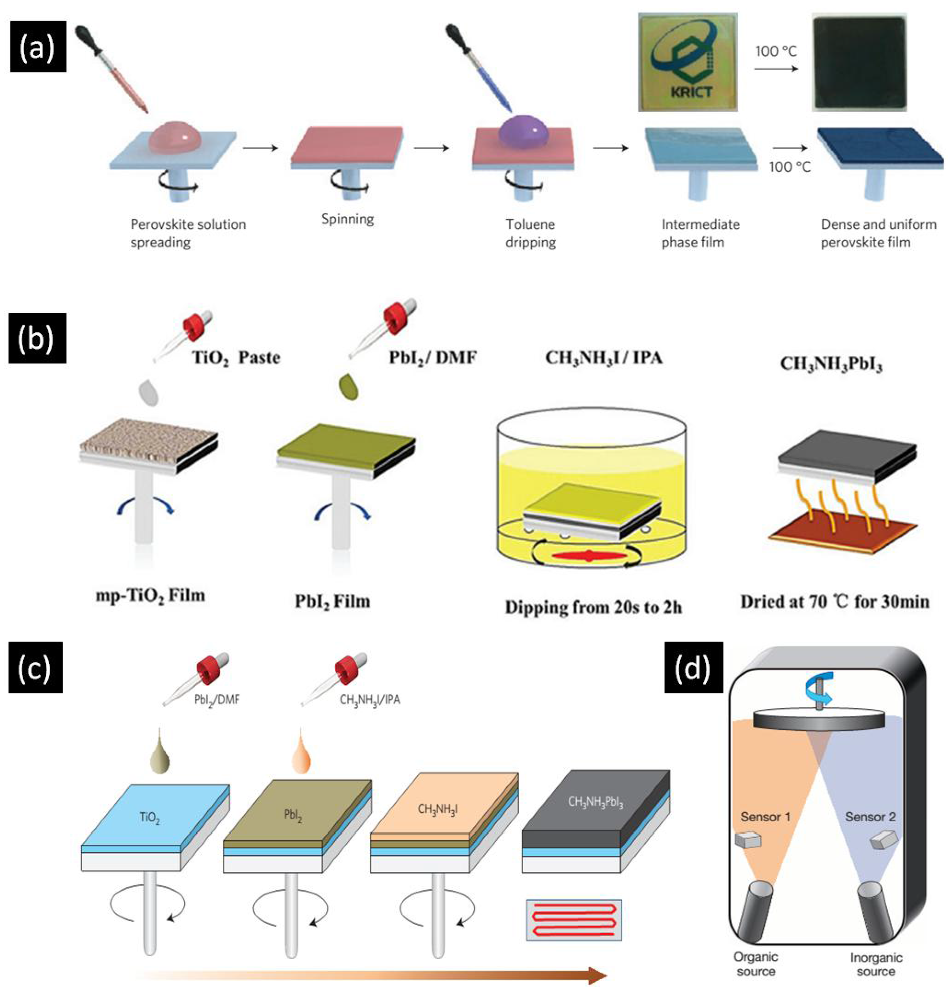
Figure 4.
Time-resolved photoluminescence (along with stretched exponential fits) of MAPbI3 using the electron quencher [6,6]-phenyl-C61-butyric acid methyl ester (PCBM) shown as blue trianges or using the hole quencher layer Spiro-MeOTAD, shown as red circles. The data obtained without the use of a quencher, instead using insulating polymer poly(methylmethacrylate) (PMMA) is shown as black squares. Adapted from Ref. [53] with permission from The American Association for the Advancement in Science.

Figure 5.
Energy level diagrams illustrating the position of the conduction band minimum vs. the vacuum level in various electron transport layer materials. Adapted from Ref. [77] with permission from The Royal Society of Chemistry.
Figure 5.
Energy level diagrams illustrating the position of the conduction band minimum vs. the vacuum level in various electron transport layer materials. Adapted from Ref. [77] with permission from The Royal Society of Chemistry.

Figure 6.
(a) IMPS and (b) IMVS plots of TiO2 nanoparticle and NT based DSSCs to calculate transport time and recombination time respectively. Reprinted with permission from [20]. Copyright 2007 American Chemical Society.
Figure 6.
(a) IMPS and (b) IMVS plots of TiO2 nanoparticle and NT based DSSCs to calculate transport time and recombination time respectively. Reprinted with permission from [20]. Copyright 2007 American Chemical Society.

Figure 7.
(a) Open circuit voltage decay plots and (b) electron recombination lifetime vs. voltage plots of MAPbI3 perovskite solar cells with different lengths of TiO2 NTs as the ETL. Reprinted with permission from Ref. [57], published by the Royal Society of Chemistry.
Figure 7.
(a) Open circuit voltage decay plots and (b) electron recombination lifetime vs. voltage plots of MAPbI3 perovskite solar cells with different lengths of TiO2 NTs as the ETL. Reprinted with permission from Ref. [57], published by the Royal Society of Chemistry.

Figure 8.
Scanning electron microscopic (SEM) images of MAPbI3 deposited on (a) TiO2 nanotubes and (b) TiO2 nanoparticles, and cross-sectional images of a complete photovoltaic device using (c) TiO2 nanotubes and (d) TiO2 nanoparticles; (e) X-ray diffraction (XRD) spectrum displaying the incomplete conversion of PbI2 using TiO2 nanotubes. Reused with permission from Ref. [105]. Copyright 2015 Wiley and Sons.

Figure 9.
Top SEM image of (a) bare FTO (b) Ti sputtered on FTO (c) anodized TiO2 and (d) cross-sectional SEM image of anodized TiO2. Reprinted with permission from Ref. [107]. Copyright 2016 American Chemical Society.
Figure 9.
Top SEM image of (a) bare FTO (b) Ti sputtered on FTO (c) anodized TiO2 and (d) cross-sectional SEM image of anodized TiO2. Reprinted with permission from Ref. [107]. Copyright 2016 American Chemical Society.
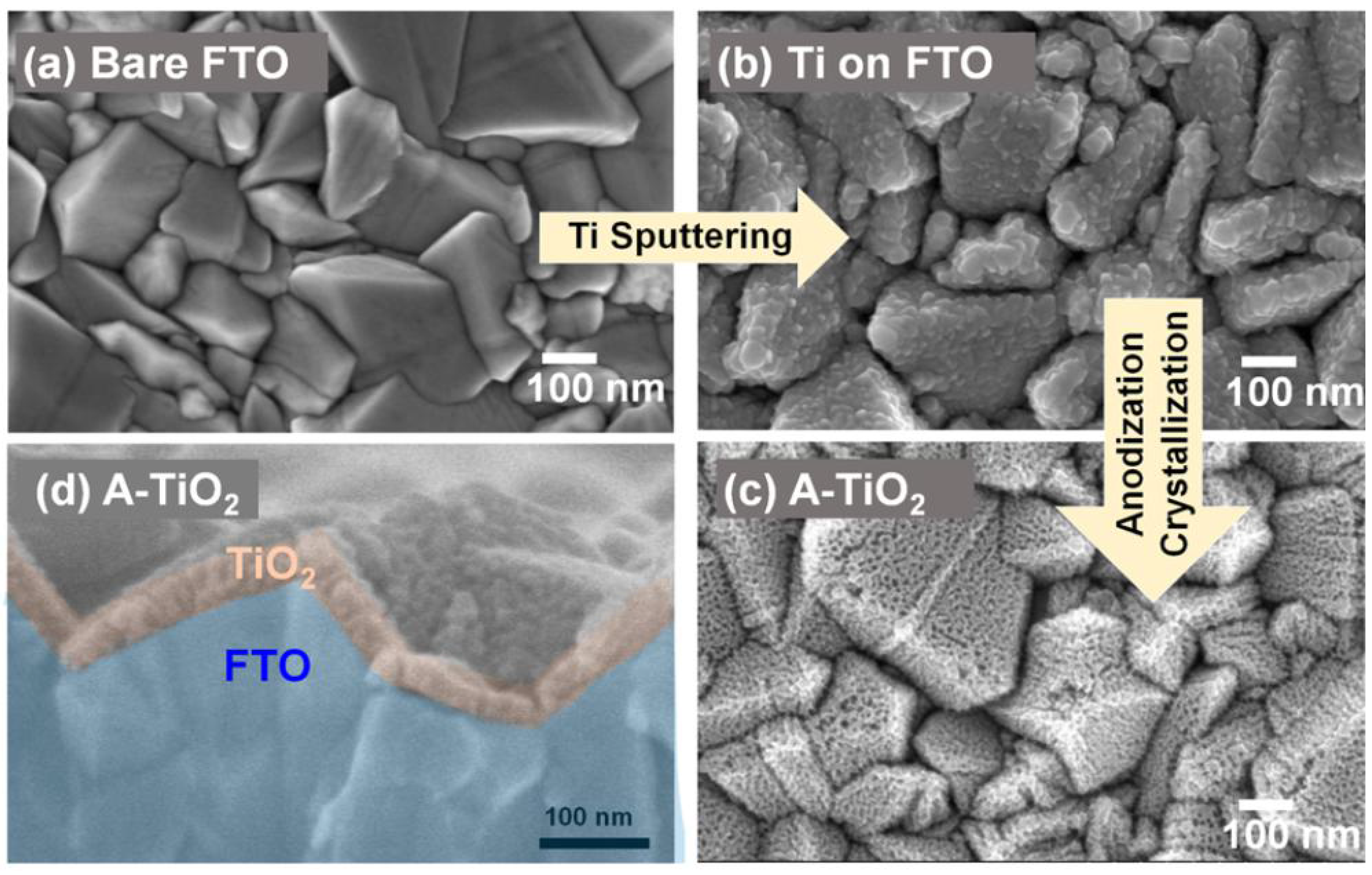
Figure 10.
(a) Top-view SEM image of TiO2 nanowires; (b) Cross-sectional SEM image of TiO2 nanowires; (c) Cross-sectional SEM image of perovskite solar cell fabricated using a TiO2 nanowire array as the ETL; and (d) J–V curve of the best performing perovskite solar cell with TiO2 nanowire array ETL. Adapted with permission from Ref. [116]. Copyright 2016 American Chemical Society.

Figure 11.
Comparison between time constant for charge recombination (τR) as a function of light intensity, represented by photocurrent density, for ZnO and TiO2 NRs. Adapted with permission from Ref. [132]. Copyright 2014 American Chemical Society.
Figure 11.
Comparison between time constant for charge recombination (τR) as a function of light intensity, represented by photocurrent density, for ZnO and TiO2 NRs. Adapted with permission from Ref. [132]. Copyright 2014 American Chemical Society.

Figure 12.
Comparison of recombination resistance of planar ZnO and ZnO nanorod-based perovskite solar cells. Adapted with permission from Ref. [130] with permission of The Royal Society of Chemistry.
Figure 12.
Comparison of recombination resistance of planar ZnO and ZnO nanorod-based perovskite solar cells. Adapted with permission from Ref. [130] with permission of The Royal Society of Chemistry.
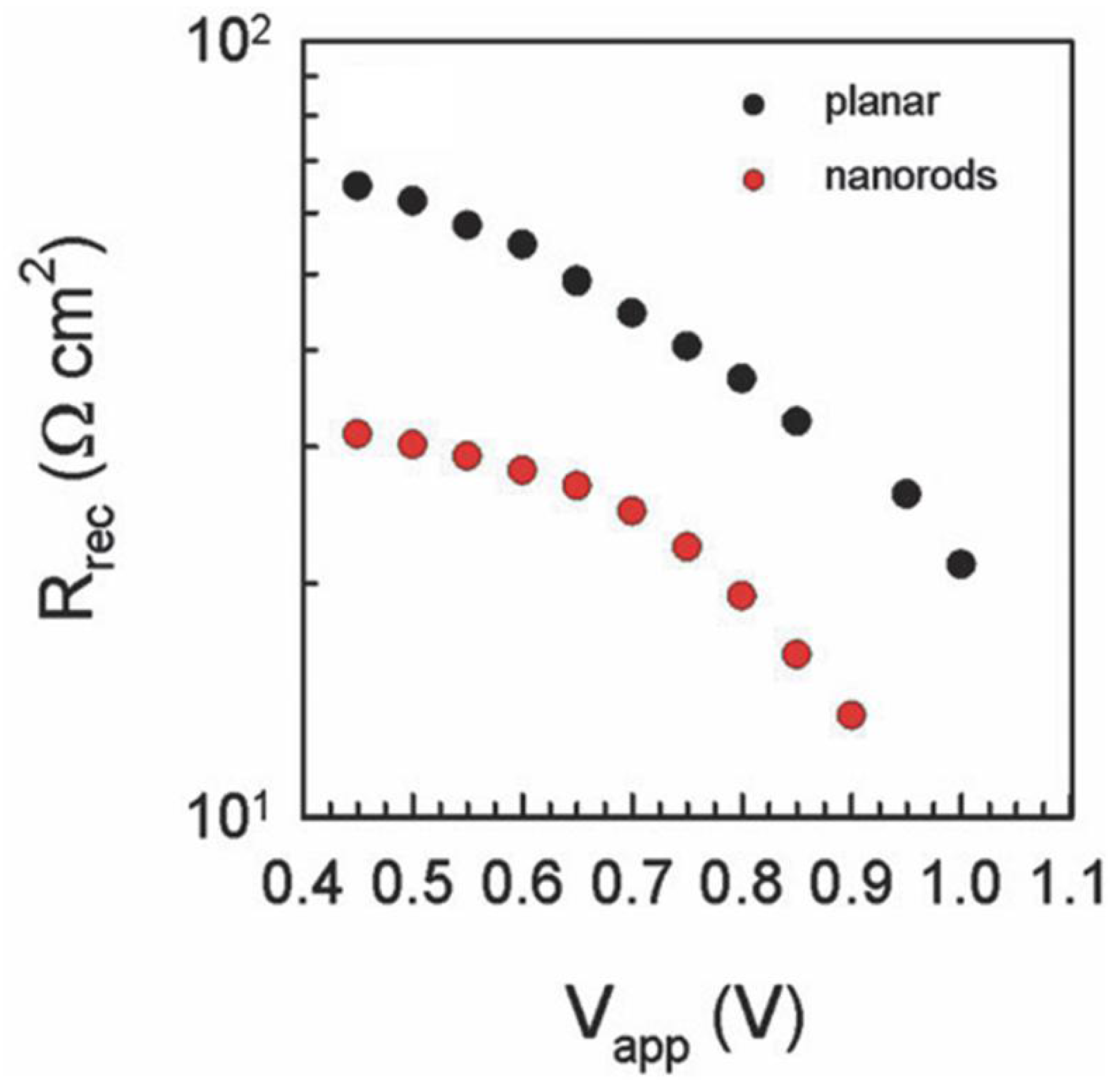
Figure 13.
(a) Schematic diagram of the Si NW array/perovskite hybrid solar cell; (b) Band alignment scheme for the Si/MAPbI3 heterostructure and (c) J–V characteristics of a Si NW array solar cell and a Si NW array/perovskite hybrid solar cell. Adapted with permission from Ref. [145] under the terms of the Creative Commons Attribution 4.0 International License.

Figure 14.
FDTD simulation results showing the simulated EM energy density distribution in MAPbI3-TiO2 NR/ND solar cells after pulse EM waves passing through: (a) perovskite–TiO2 nanodendrites (wavelength of 650 nm); (b) perovskite–TiO2 NRs (wavelength of 650 nm) and (c) IQE spectra of perovskite–TiO2 NR and perovskite–TiO2 ND solar cells. Adapted with permission from the Royal Society of Chemistry, original graphs appeared in Ref. [152].


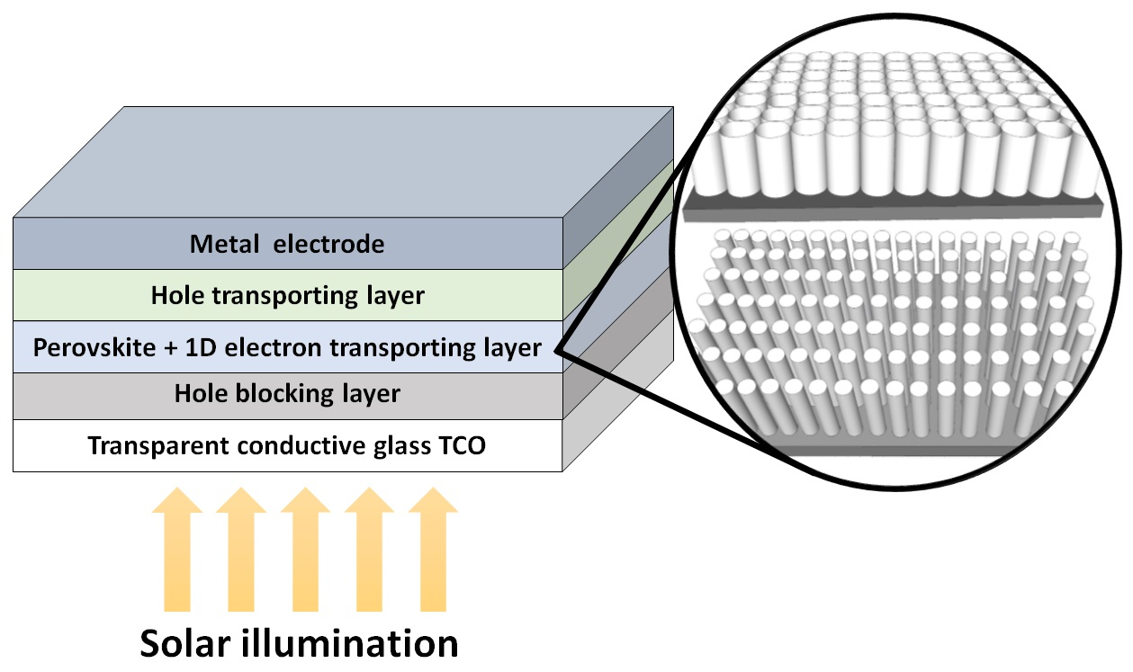
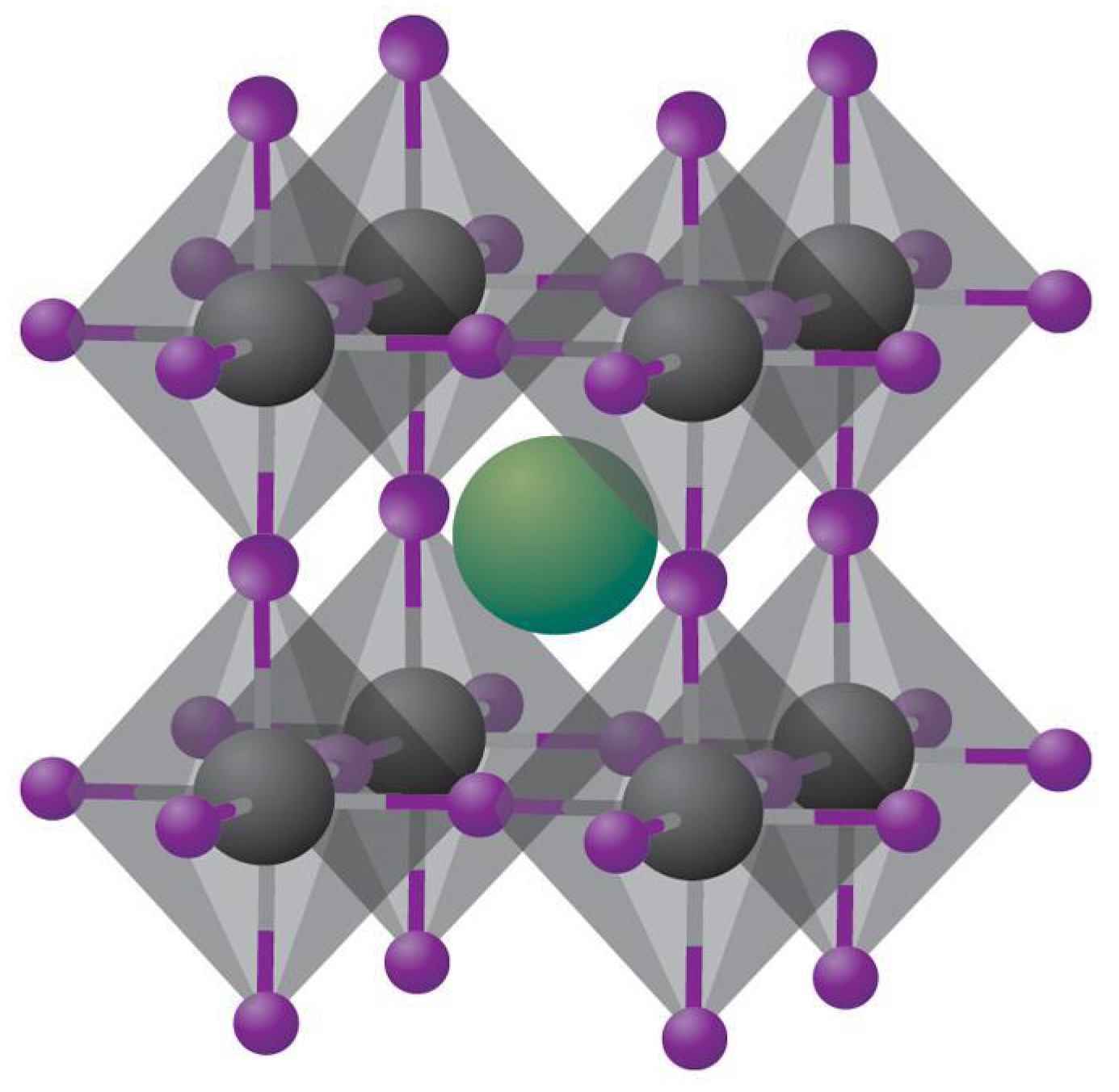
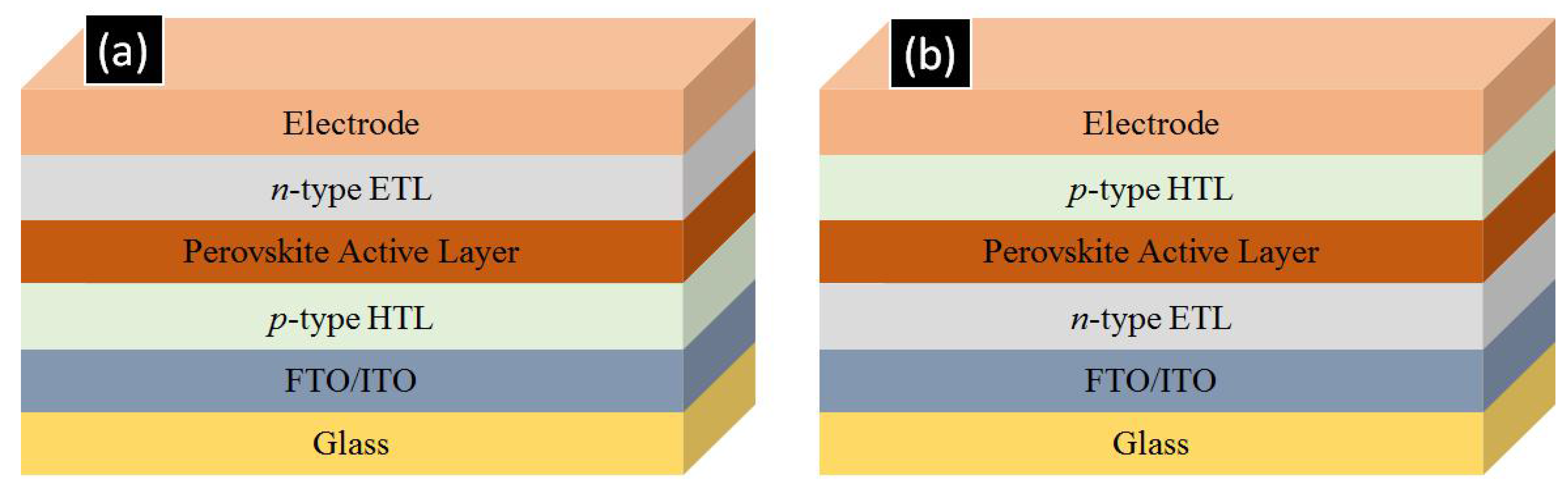
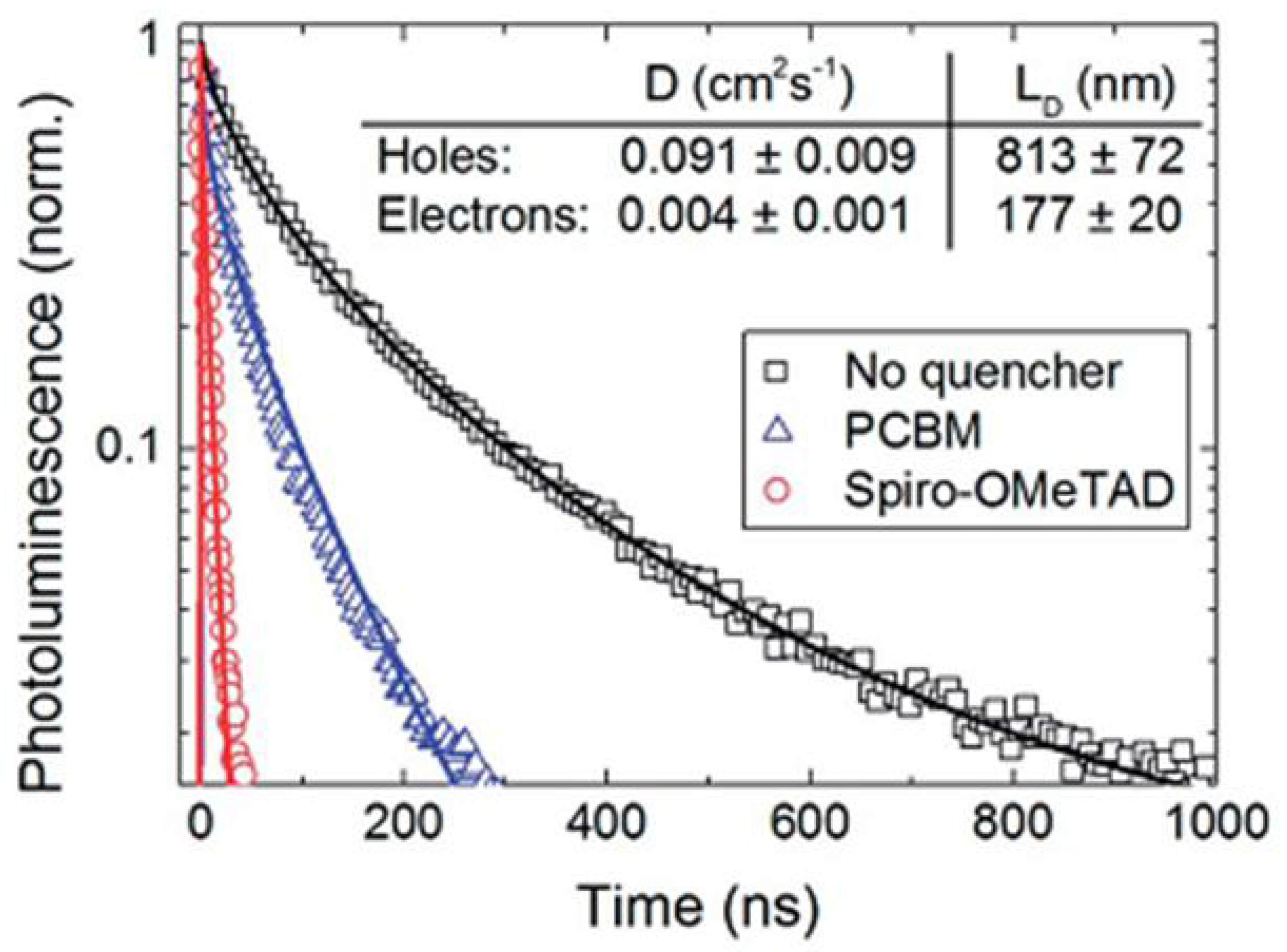
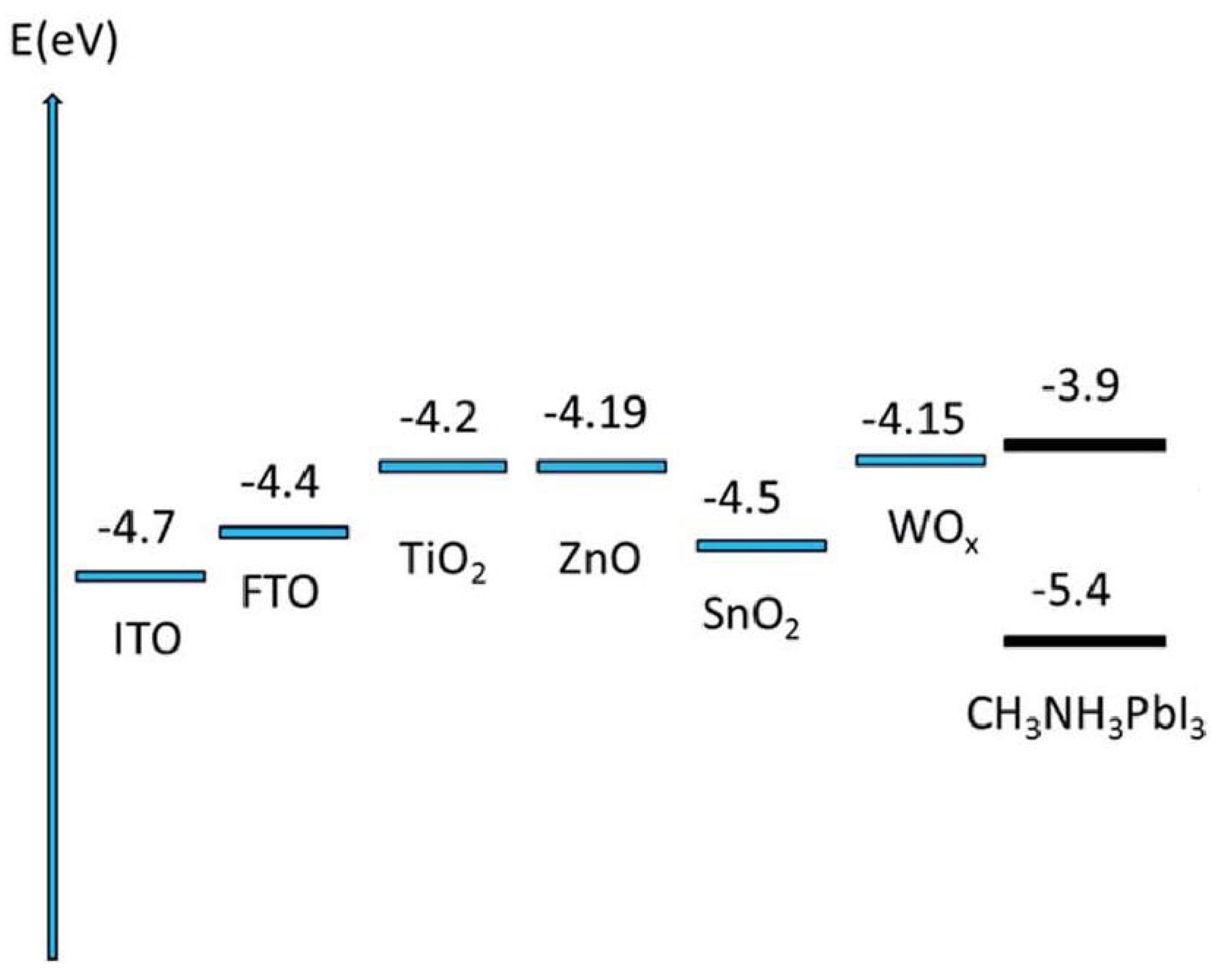
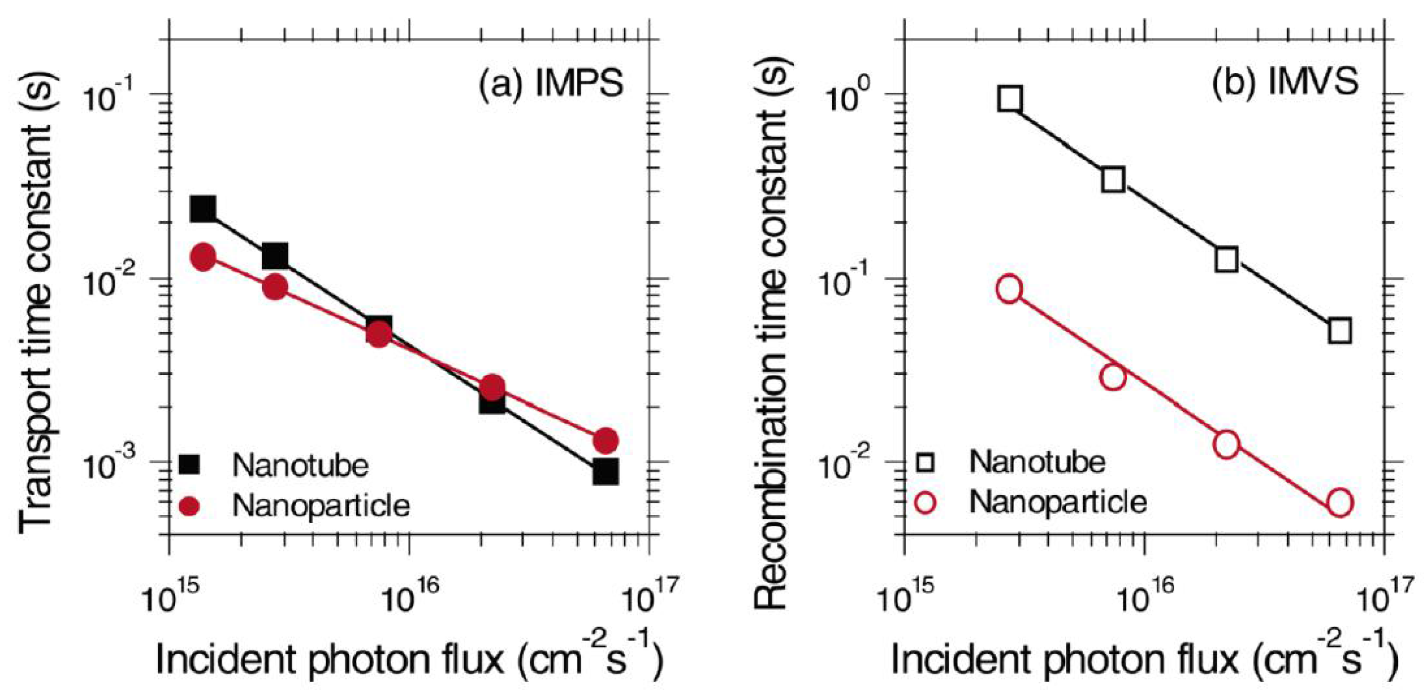
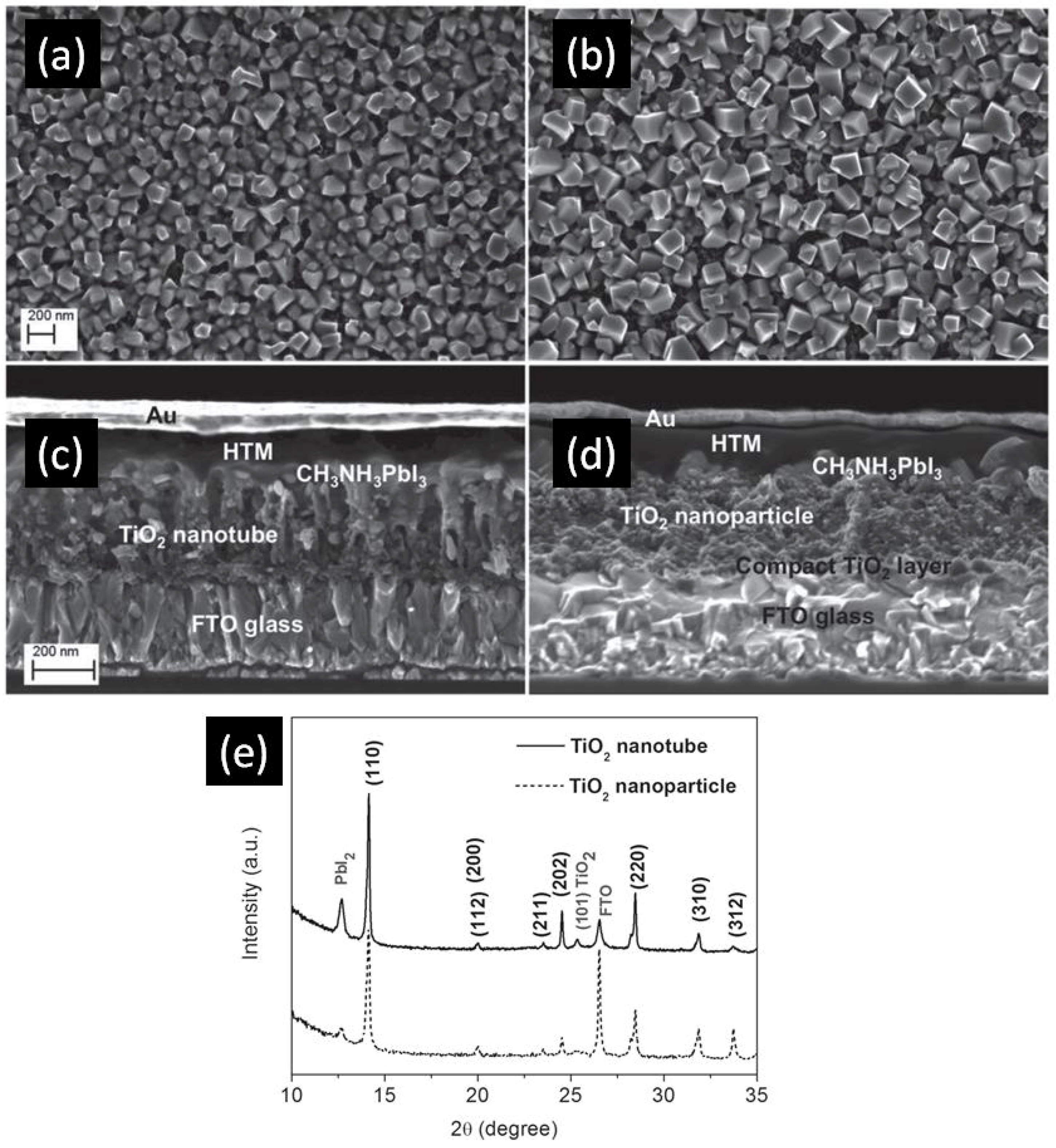
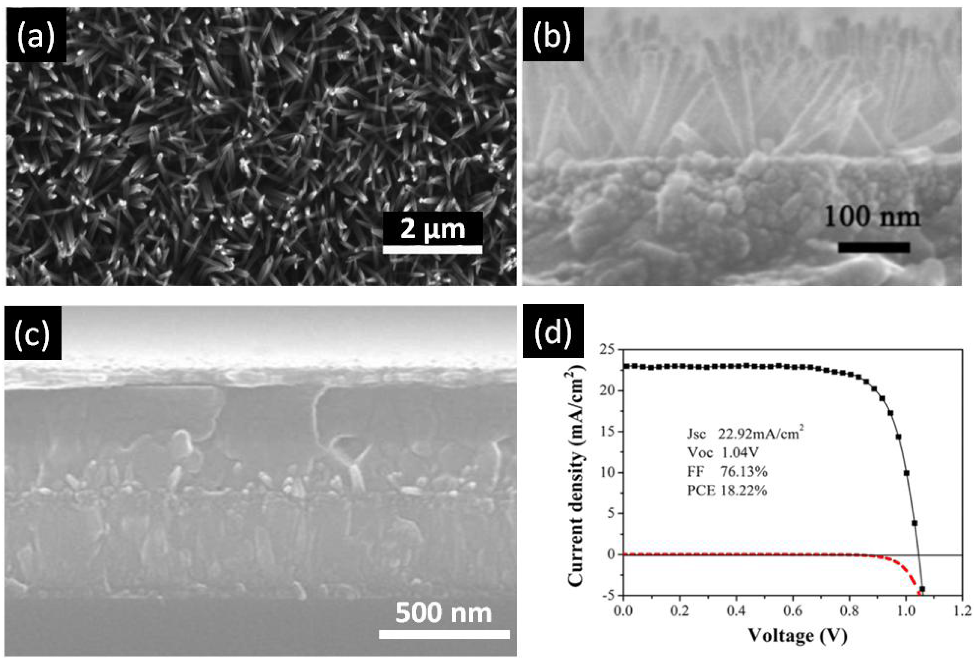
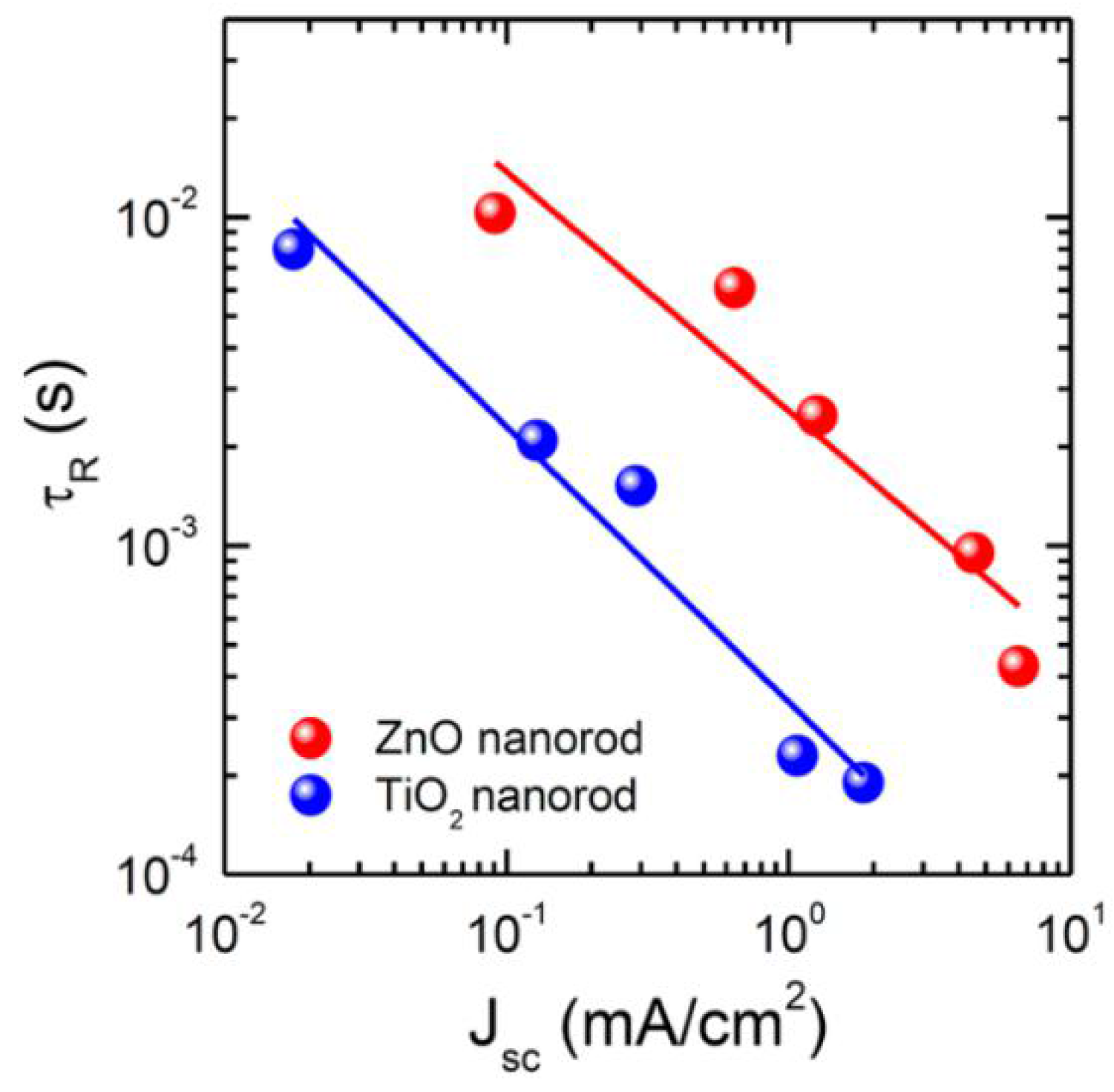
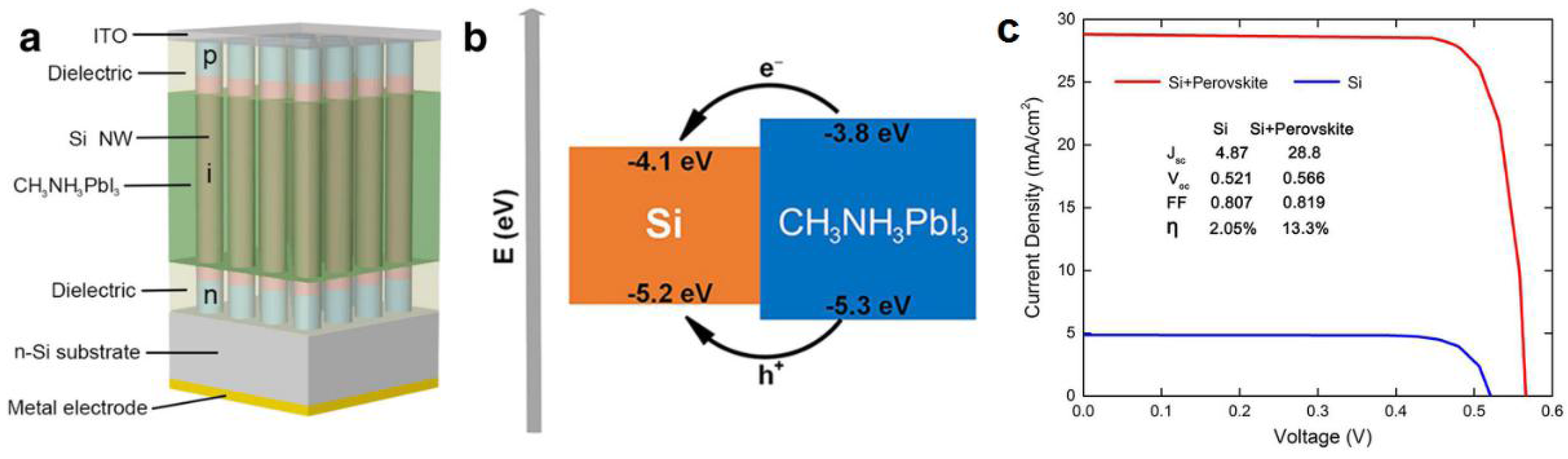
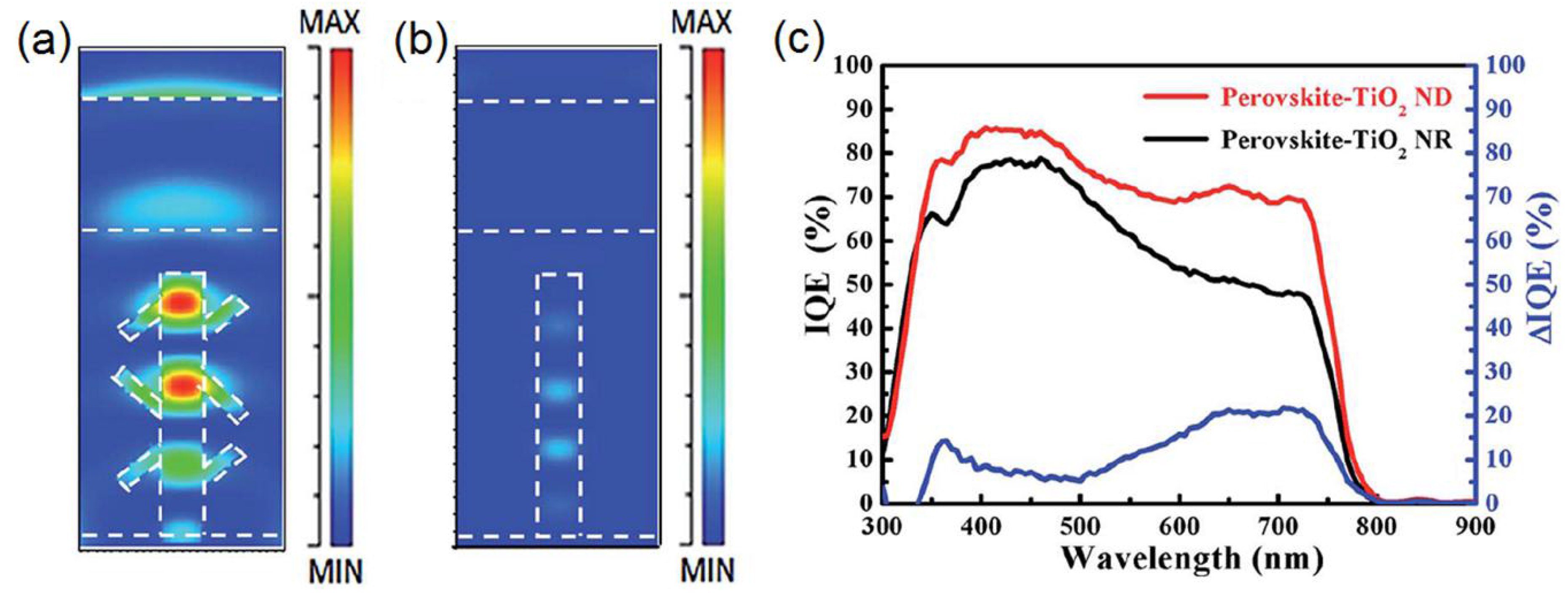
Table 1.
Summary of solar cell performance reported to date for one-dimensional TiO2 ETLs.
| Year | Device Structure | VOC (V) | JSC (mA·cm−2) | FF | PCE (%) | Ref. |
|---|---|---|---|---|---|---|
| 2013 | FTO|TiO2 BL|TiO2 NR|MAPbI3|Spiro|Au | 0.82 | 10.1 | 0.59 | 4.87 | [110] |
| 2013 | FTO|TiO2 BL|TiO2 NR|MAPbI3|Spiro|Au | 0.96 | 15.6 | 0.63 | 9.40 | [111] |
| 2014 | FTO|TiO2 BL|TiO2 NR|MAPbI3|Spiro|Au | 0.77 | 22.3 | 0.68 | 11.7 | [112] |
| 2014 | FTO|TIO2 BL|TIO2 NT| MAPbI3|Spiro | 0.63 | 17.9 | 0.58 | 6.52 | [57] |
| 2014 | FTO|TiO2 BL|Nb-TiO2 NR|MAPbIxBr3-x|Spiro|Au | 0.87 | 16.5 | 0.52 | 7.50 | [113] |
| 2014 | FTO|TiO2 BL|Sn-TiO2 NR|MAPbI3|Spiro|Ag | 0.74 | 14.9 | 0.52 | 6.31 | [114] |
| 2015 | FTO|TiO2 BL|TiO2 NR/Layer|MAPbI3|Spiro|Au | 0.95 | 19.8 | 0.72 | 13.5 | [115,116] |
| 2015 | FTO|TiO2 NT|MAPbI3|Spiro|Au | 1.07 | 22.6 | 0.64 | 14.8 | [105] |
| 2015 | FTO|TiO2 BL|TIO2 NT|MAPbI3|Au | 0.67 | 19.6 | 0.37 | 5.00 | [109] |
| 2015 | Ti|TiO2 NT|MAPbI3|CNT Film|Spiro | 0.99 | 14.4 | 0.68 | 8.31 | [108] |
| 2016 | FTO|TiO2 BL|TiO2 NR|MAPbI3|Spiro|Au | 1.04 | 22.9 | 0.76 | 18.2 | [116] |
| 2016 | FTO|TiO2 NT|MAPbI3-xAcx|Ag | 1.06 | 20.5 | 0.7 | 15.2 | [107] |
| 2017 | FTO|TiO2 BL|TiO2 NT network|MAPbI3|Ag | 0.88 | 24.8 | 0.63 | 13.8 | [106] |
Table 2.
Summary of solar cell performance reported to date for one dimensional ZnO ETLs.
| Year | Device Structure | VOC (V) | JSC (mA·cm−2) | FF | PCE (%) | Ref. |
|---|---|---|---|---|---|---|
| 2013 | FTO|ZnO NW|MAPbI3|Spiro|Ag | 0.68 | 12.7 | 0.58 | 5.00 | [55] |
| 2013 | FTO|ZnO SL|ZnO NW|MAPbI3|Spiro|Au | 1.02 | 17.0 | 0.51 | 8.90 | [130] |
| 2014 | FTO|ZnO SL|ZnO NW|AZO|MAPbI3|Spiro|Au | 0.90 | 19.8 | 0.60 | 10.7 | [131] |
| 2014 | FTO|ZnO SL|ZnO NW|MAPbI3|Spiro|Au | 0.99 | 20.1 | 0.56 | 11.1 | [132] |
| 2014 | FTO|ZnO NR|MAPbI3|Spiro|MoO3|Ag | 1.04 | 22.4 | 0.57 | 13.4 | [133] |
| 2014 | FTO|TiO2|ZnO SL|ZnO NW|MAPbI3|Spiro|Ag | 0.93 | 18.0 | 0.62 | 10.4 | [134] |
| 2014 | FTO|ZnO NR|PEI|MAPbI3|Spiro|Ag | 0.97 | 21.7 | 0.70 | 16.2 | [60] |
| 2015 | FTO|ZnO NW|TiO2 core shell|MAPbI3|Spiro|Au | 1.00 | 22.0 | 0.70 | 15.4 | [61] |
| 2016 | FTO|ZnO SL|ZnO NR|MAPbI3|Spiro|Au | 0.68 | 21.6 | 0.62 | 9.06 | [135] |
| 2016 | FTO|ZnO NR|SnO2|Spiro|Ag | 0.90 | 23.3 | 0.57 | 12.2 | [76] |
| 2016 | AZO|ZnO NR|MAPbIxCl3-x|Carbon | 0.86 | 14.9 | 0.28 | 3.62 | [136] |
| 2016 | FTO|ZnO-TiO2 NW|ZrO2|MAPbI3|Carbon | 0.96 | 14.8 | 0.58 | 8.24 | [137] |
| 2016 | ITO|Ni-ZnO NW|PCBM|(MA)x(GA)1-xPbI3|P3HT|Au | 0.83 | 23.7 | 0.70 | 13.8 | [34] |
| 2016 | FTO|ZnO SL|ZnO NW|PCBM| MAPbI3|Spiro|Au | 0.96 | 22.1 | 0.55 | 11.7 | [138] |
Table 3.
Summary of reported device performances from solar cells incorporating ETLs containing composites and unusual morphologies.
Table 3.
Summary of reported device performances from solar cells incorporating ETLs containing composites and unusual morphologies.
| Year | Device Structure | VOC (V) | JSC (mA·cm−2) | FF | PCE (%) | Ref. |
|---|---|---|---|---|---|---|
| 2016 | FTO|ZnO-TiO2 NW|ZrO2|MAPbI3|Carbon | 0.96 | 14.8 | 0.58 | 8.24 | [137] |
| 2016 | ITO|Ni-ZnO NW|PCBM|(MA)x(GA)1-xPbI3|P3HT|Au | 0.83 | 23.7 | 0.70 | 13.8 | [34] |
| 2015 | FTO|ZnO NW|TiO2 core shell|MAPbI3|Spiro|Au | 1.00 | 22.0 | 0.70 | 15.4 | [61] |
| 2014 | FTO|TiO2|ZnO SL|ZnO NW|MAPbI3|Spiro|Ag | 0.93 | 18.0 | 0.62 | 10.4 | [134] |
| 2014 | FTO|TiO2 BL/SL|Nb-TiO2 NR|MAPbIxBr1-x|Spiro|Au | 0.87 | 16.5 | 0.52 | 7.50 | [113] |
| 2014 | FTO|TiO2 SL|Sn-TiO2 NR|MAPbI3|Spiro|Ag | 0.74 | 14.9 | 0.52 | 6.31 | [114] |
| 2015 | FTO|TiO2 BL|TiO2 NR/Layer|MAPbI3|Spiro|Au | 0.95 | 19.8 | 0.72 | 13.5 | [115] |
| 2015 | FTO|WO3 BL|WO3 NR|TiO2|MAPbI3|Spiro|Ag | 0.86 | 15.00 | 0.70 | 9.10 | [38] |
© 2017 by the authors. Licensee MDPI, Basel, Switzerland. This article is an open access article distributed under the terms and conditions of the Creative Commons Attribution (CC BY) license (http://creativecommons.org/licenses/by/4.0/).
Share and Cite
MDPI and ACS Style
Thakur, U.K.; Kisslinger, R.; Shankar, K. One-Dimensional Electron Transport Layers for Perovskite Solar Cells. Nanomaterials 2017, 7, 95. https://doi.org/10.3390/nano7050095
AMA Style
Thakur UK, Kisslinger R, Shankar K. One-Dimensional Electron Transport Layers for Perovskite Solar Cells. Nanomaterials. 2017; 7(5):95. https://doi.org/10.3390/nano7050095
Chicago/Turabian StyleThakur, Ujwal K., Ryan Kisslinger, and Karthik Shankar. 2017. "One-Dimensional Electron Transport Layers for Perovskite Solar Cells" Nanomaterials 7, no. 5: 95. https://doi.org/10.3390/nano7050095
Note that from the first issue of 2016, this journal uses article numbers instead of page numbers. See further details here.